Embed Size (px)
Citation preview
Scanning Electron MicroscopyScanning Electron Microscopy
Instrument
Imaging
Chemical Analysis (EDX)
Structural and Chemical Analysis of Materials
J.P. EberhartJohn Wiley & Sons, Chichester, England, 1991.
Scanning Electron Microscopy and X-Ray Microanalysis
J. Goldstein, D. Newbury, D. Joy, C. Lyman, P. Echlin, E. Lifshin, L. Sawyer, J. Michael
Kluwer
Academic/Plenum Publishers, New York, 2003.

1.
A column which generates a beam of electrons.
2.
A specimen chamber where the electron beam interacts with the sample.
3.
Detectors to monitor the different signals that result from the electron beam/sample interaction.
4.
A viewing system that builds an image from the detector signal.
32
14

Reduced image of crossover
Project the crossover image onto the specimen
X-Y
translation + rotation
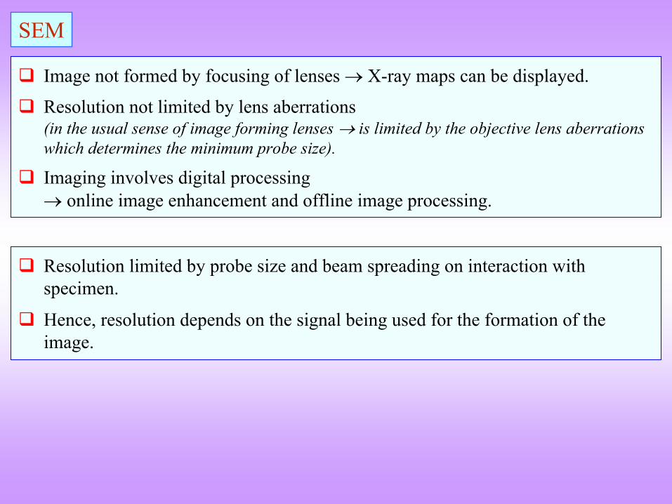
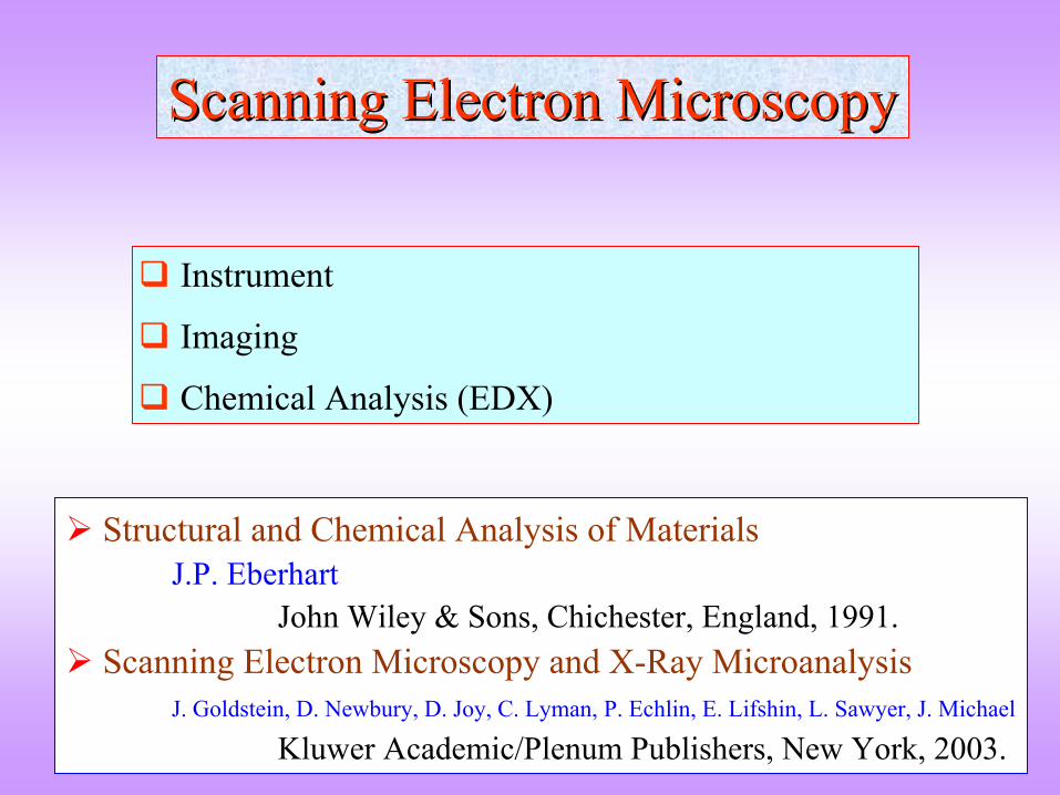
Image not formed by focusing of lenses X-ray maps can be displayed.
Resolution not limited by lens aberrations (in the usual sense of image forming lenses is limited by the objective lens aberrations which determines the minimum probe size).
Imaging involves digital processing online image enhancement and offline image processing.
SEM
Resolution limited by probe size and beam spreading on interaction with specimen.
Hence, resolution depends on the signal being used for the formation of the image.
A fine electron probe is scanned over the specimen.
Various detectors (Secondary Electron (SE), Back Scattered Electron (BSE), X-
Ray, Auger Electron (AE) etc.) pick up the signals.
The amplified output of a detector controls the intensity
of the electron beam of a CRT (synchronized scanning) of the pixel of display
Scanning Electron Beam Various Detectors
(SE, BSE, EDX, AE) Display on CRT
Parameter Values
Resolution ~ 40 Å
(SE); ~ (100-500) Å
(BSE)
Magnification 10 –
105
Depth of field High (~ m)
Size of specimen 1 –
5 cm (usual range)
Note that the resolution depends on the type of
signal being used
Importance of SEM

Absorbed Electrons Electron-Hole Pairs
Direct Beam
SPECIMEN
Elastically Scattered Electrons
InelasticallyScattered Electrons
Bremsstrahlung
X-
raysAuger Electrons
Visible Light
BackscatteredElectrons (BSE)
Secondary Electrons (SE)
Characteristic
X-rays
Incident High-kV Beam
In a SEM
these signals are absent
Many signals are generated by the interaction of the electron beam with the specimen. Each of these signals is sensitive to a different aspect of the specimen
and give a variety of information about the specimen.
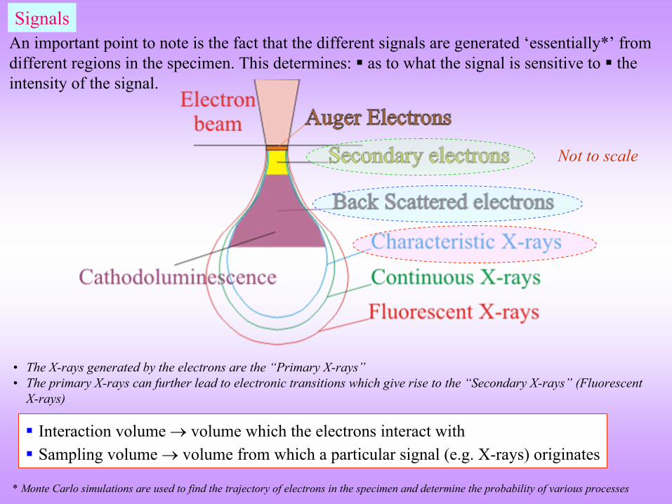
Signals
Interaction volume volume which the electrons interact with
Sampling volume volume from which a particular signal (e.g. X-rays) originates
•
The X-rays generated by the electrons are the “Primary X-rays”•
The primary X-rays can further lead to electronic transitions which give rise to the “Secondary X-rays”
(Fluorescent X-rays)
An important point to note is the fact that the different signals are generated ‘essentially*’
from different regions in the specimen. This determines:
as to what the signal is sensitive to
the intensity of the signal.
* Monte Carlo simulations are used to find the trajectory of electrons in the specimen and determine the probability of various processes
Not to scale
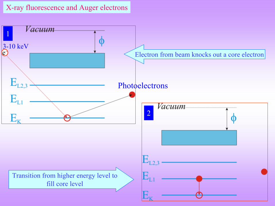
1
2
e−3-10 keV
Photoelectrons
X-ray fluorescence and Auger electrons
Electron from beam knocks out a core electron
Transition from higher energy level to fill core level

3
4
Generation of x-rays accompanying the transition
Further the x-ray could knock out an electron from an outer level → this electron is called the Auger electron

SemiconductorsConduction band
Valence band
Band gap
e
e
hole
Electron beam induced current ( EBIC)
Charge collection microscopyOR
Electron-hole pairs and cathodoluminescence
h
Bias
Cathodoluminescence
(CL) Spectroscopy
Photoluminescence Photon induced light emission
Cathodoluminescence
Electron induced light emission
Incident electron excites an electron from the valence band to the conduction band → creating an electron hole pair
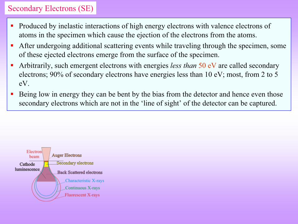
Produced by inelastic interactions of high energy electrons with
valence electrons of atoms in the specimen which cause the ejection of the electrons from the atoms.
After undergoing additional scattering events while traveling through the specimen, some of these ejected electrons emerge from the surface of the specimen.
Arbitrarily, such emergent electrons with energies less than
50 eV
are called secondary electrons; 90% of secondary electrons have energies less than 10
eV; most, from 2 to 5 eV.
Being low in energy they can be bent by the bias from the detector and hence even those secondary electrons which are not in the ‘line of sight’
of the detector can be captured.
Secondary Electrons (SE)

http://www.emal.engin.umich.edu/courses/semlectures/se1.html
SE are generated by 3 different mechanisms:
SE(I) are produced by interactions of electrons from the incident beam with specimen atoms
SE(II) are produced by interactions of high energy BSE with specimen atoms
SE(III) are produced by high energy BSE which strike pole pieces and other solid objects near the specimen.
Some Z contrast!
Secondary Electrons

Produced by elastic interactions of beam electrons with nuclei of atoms in the specimen
Energy loss less than 1 eV
Scattering angles range up to 180°, but average about 5°
Many incident electrons undergo a series of such elastic event that cause them to be scattered back out of the specimen
The fraction of beam electrons backscattered in this way varies strongly with the atomic number Z of the scattering atoms, but does not change much with changes in E0
.
http://www.emal.engin.umich.edu/courses/semlectures/se1.html
Back Scattered Electrons (BSE)
Dependence on atomic number
BSE images show atomic number contrast (features of high average Z appear brighter than those of low average Z)
BSE
IE
nn
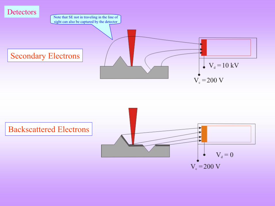
Secondary Electrons
Backscattered Electrons
DetectorsNote that SE not in traveling in the line of sight can also be captured by the detector

Magnification
The magnification in an SEM
is of ‘Geometrical origin’
(this is unlike a TEM or a optical microscope)
Probe scans a small region of the sample, which is projected to a large area (giving rise to the magnification).
Area scanned on specimen
Area projected onto display

Depth of field
Dependent on the angle of convergence of the beam
Depth of field is the same order of magnitude as the scan length
Magnification 10,000
Scan length 10 m
Depth of Field 8 m

Probe size
(probe size is dependent on many factors)
Signal being used for imaging This is because the actual interaction volume/cross section is different from the probe diameter. Additionally, each signal is sensitive to a different aspect of the specimen.
What determines the resolution in an SEM?
In terms of parameters:
Accelerating voltage
Beam current
Beam diameter
Convergence angle of beam

Inclination Effect
Shadowing Contrast
Edge/Spike Contrast
Topographic Contrast in SEM
Line of sight with the detector

Accelerating Voltage
Probe Current
Working Distance
Specimen Tilt
Aperture Size
Operating parameters affecting signal quality
Edge effect
Contamination
Charging

Operating Parameter Values
Gun voltage ~20 keV
Working distance ~26 mm
Probe size W filament ~30 Å
LaB6
Field Emission
Vacuum W filament 10−5
Torr
LaB6 10−8
Torr
Field Emission 10−10
Torr
Probe current
Probe diameter
Resolution
This leads to decrease in image intensity we have to use a brighter source
(W filament < LaB6 < Field Emission gun)
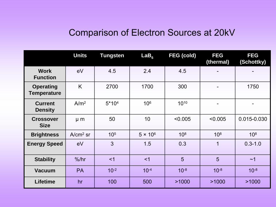
Units Tungsten LaB6 FEG (cold) FEG (thermal)
FEG (Schottky)
Work Function
eV 4.5 2.4 4.5 - -
Operating Temperature
K 2700 1700 300 - 1750
Current Density
A/m2 5*104 106 1010 - -
Crossover Size
μ
m 50 10 <0.005 <0.005 0.015-0.030
Brightness A/cm2
sr 105 5 ×
106 108 108 108
Energy Speed eV 3 1.5 0.3 1 0.3-1.0
Stability %/hr <1 <1 5 5 ~1
Vacuum PA 10-2 10-4 10-8 10-8 10-8
Lifetime hr 100 500 >1000 >1000 >1000
Comparison of Electron Sources at 20kV

Probe size
Probe Current
Working Distance
Specimen Tilt
Aperture Size
Increasing Resolution
Edge effect
Contamination
Charging
Working Distance
strength of condenser lens
Leads to Beam convergence angle spherical aberration

Any signal picked up by a detector can be converted to an electrical signal and be used of imaging
Contrast processing +ve
to –ve
contrast, gamma control etc.
Contrast quantification contour mapping, colour
mapping
Image integration signal integration over a number of scans ( SNR)
Usual image analysis phase fractions etc.
Image Processing

Backscattered Electron Images
Emission of Backscattered electrons = f(composition, surface topography, crystallinity, magnetism of the specimen)
Composition Z number
Topography and composition information is separated using detector
Crystallinity
channeling contrast (& EBSD)
(the BSE intensity changes drastically on or around Bragg’s condition)
Poorer spatial resolution

Backscattered Electron Signals
Signal A
Signal B
A + B
A −
B
Topography (TOPO)Composition (COMPO)
Detectors

20 kV, 1100 Specimen: Metallic
TOPO: A −
BCOMPO: A + B
Ref: SEM Manual, JEOL

Backscattered Electron Image (BEI)
20 kV, 1100 Specimen: Metallic
Composition via:
BEI
EDX
Secondary Electron Image (SEI)
X-ray image (Si) X-ray image (Al)
Ref: SEM Manual, JEOL

www.nanoed.org/courses/zheng_electron/Dravid_part2.pdf
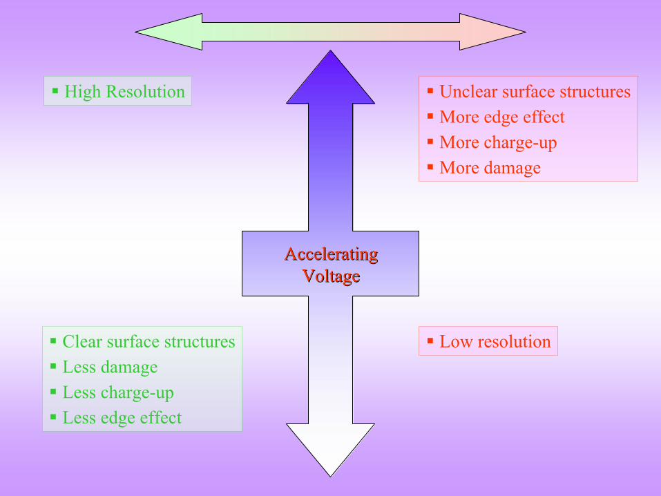
AcceleratingAccelerating
VoltageVoltage
High Resolution
Unclear surface structures
More edge effect
More charge-up
More damage
Clear surface structures
Less damage
Less charge-up
Less edge effect
Low resolution

Low atomic number High atomic number
Low accelerating
voltage
High accelerating
voltage
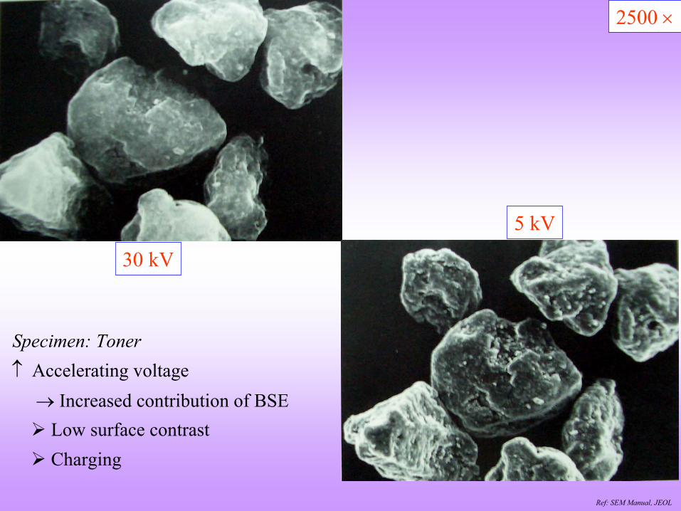
30 kV
5 kV
2500
Specimen: Toner
Accelerating voltage Increased contribution of BSE
Low surface contrast
Charging
Ref: SEM Manual, JEOL

25 kV5 kV
7200
Specimen: Sintered powder
Accelerating voltage
Better surface contrast
Not sharp at high magnifications WD or probe diameter
Ref: SEM Manual, JEOL

25 kV
5 kV
36000
Specimen: Evaporated Au particles
Accelerating voltage
Better image sharpness
Improved resolution
Ref: SEM Manual, JEOL
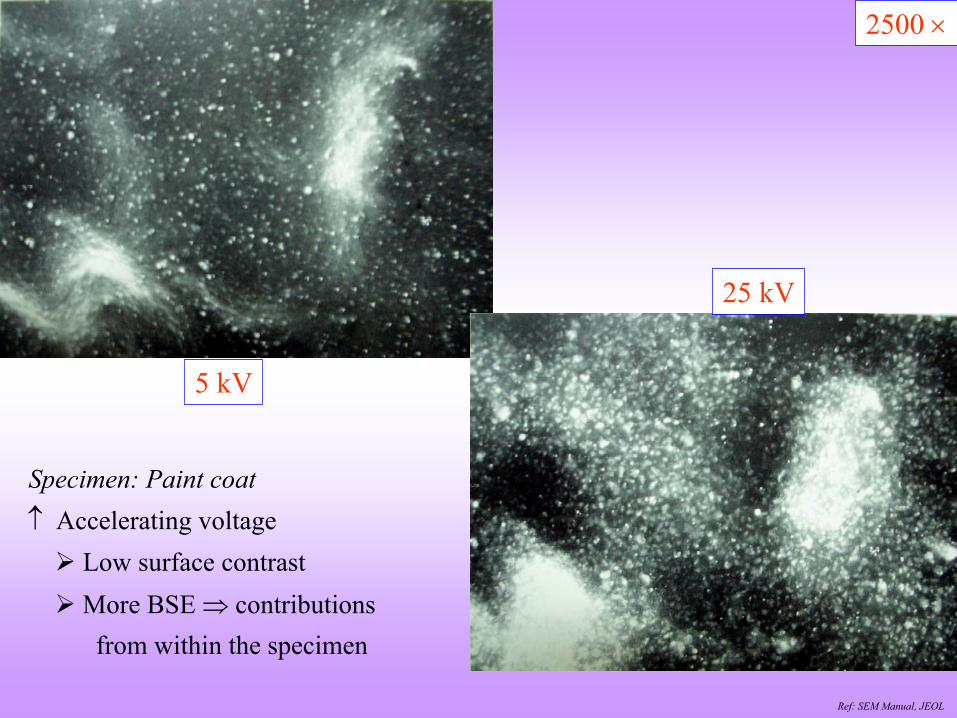
25 kV
5 kV
2500
Specimen: Paint coat
Accelerating voltage
Low surface contrast
More BSE contributions
from within the specimen
Ref: SEM Manual, JEOL

Specimen tilt
0
5kV, 1100
Specimen: IC chipTILT
Improve quality of SE images
complete survey of topography
Stereo images images at 2 angles
45
Ref: SEM Manual, JEOL

Probe currentProbe current
Smooth image
Deteriorated resolution
More damage
High-resolution obtainable
Grainy image

1 nA
10 kV, 5400
Specimen: Ceramic
Probe current
image sharpness
surface smoothness10 pA
0.1 nA
Ref: SEM Manual, JEOL

Working DistanceWorking Distance
Greater depth of field
Low depth of field
Low resolution
High resolution
The working distance is the distance between the final condenser
lens and the specimen
working distance
spherical aberration
(spot size
resolution improves) working distance
Depth of field
(wide cone of electrons)

Aperture sizeAperture size
(objective lens)(objective lens)
Large current
Grainy image
Low resolution
Smaller depth of field
High resolution
Greater depth of field
e.g. Better for EDX

Edge Effect
25 kV5 kV
Tilt: 50, 720
Accelerating voltage
Greater the edge effect (edges become brighter)
SE emission from protrusions and circumferences appear bright
Ref: SEM Manual, JEOLSpecimen: IC chip
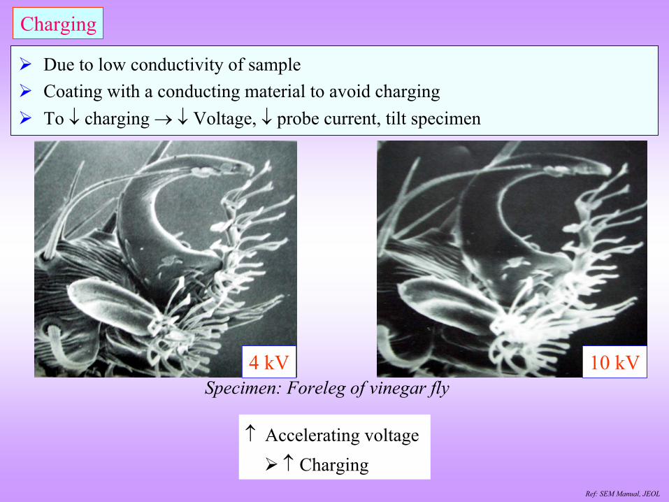
Charging
Due to low conductivity of sample
Coating with a conducting material to avoid charging
To
charging Voltage,
probe current, tilt specimen
10 kV4 kV
Accelerating voltage
ChargingRef: SEM Manual, JEOL
Specimen: Foreleg of vinegar fly

Contamination
Due to residual gas in the vicinity of the electron probe
Leads to reduced contrast and loss in image sharpness
Usually caused by scanning a small region for long time
Specimen: ITO
5 kV 18000
Contamination
Ref: SEM Manual, JEOL


Backscattered Electron Diffraction
Diffraction of Backscattered electrons:
1) Channeling contrast, 2) Diffraction patterns (EBSD)
Weaker than atomic number contrast required good BSE detector
The BSE intensity changes drastically on or around Bragg’s condition
Poorer spatial resolution
EBSD
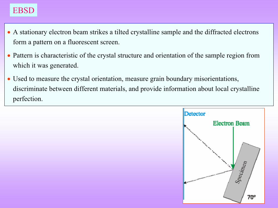
A stationary electron beam strikes a tilted crystalline sample and the diffracted electrons form a pattern on a fluorescent screen.
Pattern is characteristic of the crystal structure and orientation of the sample region from which it was generated.
Used to measure the crystal orientation, measure grain boundary misorientations, discriminate between different materials, and provide information about local crystalline perfection.

http://www.ebsd.com/basicsofebsd2.htm
A diffraction pattern from nickel collected at 20 kV accelerating voltage
http://www.ebsd.com/basicsofebsd3.htm

The nickel crystal unit cell superimposed on the diffraction pattern in the orientation which generates this pattern. The crystal planes are labelled
which correspond to the (2-20) and (020) Kikuchi bands in the diffraction pattern.
Indexing: Kikuchi bands are labelled
with the Miller indices of the crystal planes that generated them (red). The planes project onto the screen at the centre of the bands. Kikuchi band intersections are labelled
with crystal direction that meets the screen at this point (white). This direction is the zone axis of the planes corresponding to the intersecting Kikuchi bands.
The Kikuchi band width depends on the d-spacing of the corresponding plane. The (200) plane d-spacing is wider than the (2-20) plane so the Kikuchi bands from (200) planes are narrower than those from (2-20) planes.
http://www.ebsd.com/basicsofebsd3.htm
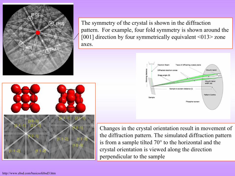
The symmetry of the crystal is shown in the diffraction pattern. For example, four fold symmetry is shown around the [001] direction by four symmetrically equivalent <013> zone axes.
http://www.ebsd.com/basicsofebsd3.htm
Changes in the crystal orientation result in movement of the diffraction pattern. The simulated diffraction pattern is from a sample tilted 70°
to the horizontal and the crystal orientation is viewed along the direction perpendicular to the sample


![Ultrafast transmission electron microscopy using a laser ...transmission electron microscopy [4], scanning electron microscopy [5], x-ray diffraction [6], scanning tunneling and atomic](https://img.dokumen.tips/doc/110x75/607eb1335ce8082131294459/ultrafast-transmission-electron-microscopy-using-a-laser-transmission-electron.jpg)