Embed Size (px)
Citation preview

Confidential
Protium S1 – FPGA-based prototyping made easy
Volker Wegner, Staff Application EngineerTensilica DayHannover, GermanyFebruary 07, 2018

2 © 2018 Cadence Design Systems, Inc. Cadence confidential.
30 years of innovation in emulation
Mercury3.5 Mgates
550 KHz
CoBALTPlus
14 Mgates200 KHz
Palladium128 Mgates
500 KHz
System Realizer3 Mgates450 KHz
RPM
50K Gates
100Khz
Enterprise
MARS
1M Gates
200Khz
CoBALT8 Mgates100 KHz
CoBALT Ultra128 Mgates
400 KHz
MercuryPlus
10 Mgates750 KHz
Palladium II256 Mgates
750KHz
1987 to 2009
1995 to 2016
Palladium III256 Mgates
1 MHz
Xtreme III
72 Mgates600 KHz
Xtreme Server
36 Mgates300 KHz
FPGA-based Architecture
Processor-based Architecture
Palladium XP2048 Mgates
1.2MHz
Palladium XP II2304 Mgates
1.4MHz
Verification
Computing
Platforms
2000
Quickturn
2005
Verisity/Axis
Palladium Z13304 Mgates
1.6MHz
Protium S1600 Mgates10-100 MHz
RPP25 Mgates5-10 MHz
2011 2014 2017
Protium100 Mgates5-50 MHz
3 © 2018 Cadence Design Systems, Inc. Cadence confidential.
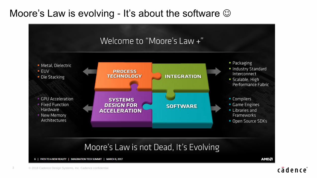
Moore’s Law is evolving - It’s about the software ☺

4 © 2018 Cadence Design Systems, Inc. Cadence confidential.
System & chip design in 2017 - 2020
LPDDR
DRAM
NAND
FLASH
NAND
FLASH
Cellular
Modem
W iFi
LLI
DigRF
LP
DD
R 2
eM
MC
4.5
UF
S
LP
DD
R 3
SD
3.0
SD
4.0
UF
S
SLIMbus
DSI
CSI2
CSI3
Bluetooth
SDIO
FM
Receiver
GPS
Receiver
RF
FE
SL
IMb
us
Motion
Sensors
cJTAG
GBT
SP
MI
Power
Control
Multimedia
Processor
I2C
US
B 2
.0
Memory
Card
HDMI 1.4
Touch Screen
Controller
Display
Driver
Audio
Interface
Camera
Interface
USB 3.0 OTG
OCP 2.0
OCP 3.0
System on Printed Circuit Board (PCB)
Application Specific Components
SoC Interconnect Fabric
ARM CPU Subsystem
3D
GFX
DSP
A/V
High speed, wired interface peripherals
D
D
R
3
P
H
Y
Other peripherals
S
A
T
A
M
IP
I
H
D
M
I
W
L
A
N
L
T
E
Low-speed peripheral
subsystem
Low speed peripherals
P
M
U
M
I
P
I
J
T
A
G
I
N
T
C
I
2
C
S
P
I
T
i
m
e
r
G
P
I
O
Display
U
A
R
T
Apps
Accel
Modem
Cortex
-A15
L2 cache
USB3.0
3
.
0
P
H
Y
2
.
0
P
H
Y
PCIe
Gen 2,3
PHY
E
t
h
e
r
n
e
t
P
H
Y
Cortex
-A15
Cortex
-A7
L2 cache
Cortex
A-A7
Cache Coherent Fabric
System on Chip (SOC)
Software
Bare
Me
tal
So
ftw
are
DS
P S
oft
wa
re
Bare
Me
tal
So
fwta
re
RTOS
Drivers
Communications L2
Communications L1
Firmware / HAL
Communications L3
Modem Comms
Application
Processor
Bare Metal
Operating Systems (OS)
Drivers
Applications
Middleware
Firmware / HAL
▪ Time-to-market
▪ Development cost reduction
▪ Multi-core design and verification
complexity
▪ Integration of new designs and
derivatives
▪ Software stack development
▪ Hardware-software convergence
▪ More than 80% re-use
▪ More than 60% of effort in software
5 © 2018 Cadence Design Systems, Inc. Cadence confidential.
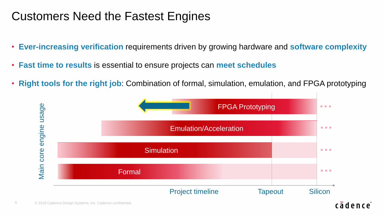
Customers Need the Fastest Engines
• Ever-increasing verification requirements driven by growing hardware and software complexity
• Fast time to results is essential to ensure projects can meet schedules
• Right tools for the right job: Combination of formal, simulation, emulation, and FPGA prototyping
Project timeline
Formal
Simulation
FPGA Prototyping
Emulation/Acceleration
Tapeout
Main
core
engin
e u
sage
Silicon
…
…
…
…

6 © 2018 Cadence Design Systems, Inc. Cadence confidential.
There is no “One Size Fits All”Verification and software platforms need to interoperate
SDK OS Simulation
•Highest speed
•Earliest in the flow
•Ignore hardware
Virtual Platform
•Almost at speed
•Less accurate (or slower)
•Before RTL
•Great to debug (but less detail)
•Easy replication
Formal Analysis
•Non-scalable
•Exhaustive
•Early RTL
•Great for IP
•No SW execution
HDL Simulation
•KHz range
•Accurate
•Excellent HW debug
•Broadly available
• Mixed-abstractions
•Limited SW execution
AccelerationEmulation
•MHz Range
•RTL accurate
•After RTL is available
•Good to debug with full detail
•Expensive to replicate
FPGA Prototype
•10’s of MHz
•RTL accurate
•After stable RTL is available
•OK to debug
•More expensive than software to replicate
Prototyping Board
•Real time speed
•Fully accurate
•Post Silicon
•Difficult to debug
•Sometimes hard to replicate

7 © 2018 Cadence Design Systems, Inc. Cadence confidential.
Cadence Verification SuiteTechnology innovation leadership: Fast, Smart, and Optimized
VIPVERIFICATION IP
Perspec™
SW-DRIVEN TEST
vManager™
METRICS
Indago™
DEBUGUniform multi-engine verificationVerification Fabric
Palladium® Z1
EMULATION
ACCELERATION
Xcelium™
SIMULATION
JasperGold®
FORMAL & STATIC
Protium™ S1
FPGA PROTOTYPE
Total throughput
Metric driven signoff
Application optimized
Cloud centric architecture
• Fast Best-in-class engines
• Smart Flow-driven engine
integrations
• Optimized comprehensive
solutions
8 © 2018 Cadence Design Systems, Inc. Cadence confidential.
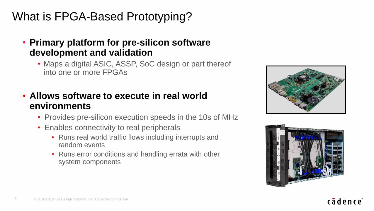
What is FPGA-Based Prototyping?
• Primary platform for pre-silicon software development and validation
• Maps a digital ASIC, ASSP, SoC design or part thereof into one or more FPGAs
• Allows software to execute in real world environments
• Provides pre-silicon execution speeds in the 10s of MHz
• Enables connectivity to real peripherals
• Runs real world traffic flows including interrupts and random events
• Runs error conditions and handling errata with other system components

9 © 2018 Cadence Design Systems, Inc. Cadence confidential.
Case study: Amlogic

10 © 2018 Cadence Design Systems, Inc. Cadence confidential.
Case study: Amlogic (cont.)

11 © 2018 Cadence Design Systems, Inc. Cadence confidential.
Case study: Amlogic (cont.)

13 © 2018 Cadence Design Systems, Inc. Cadence confidential.
FPGA-Based Prototyping is Hard to Do …
Clocking Memories
Debug
Interfaces
Software

14 © 2018 Cadence Design Systems, Inc. Cadence confidential.
FPGA-Based Prototyping Is FragmentedDisjointed, lacking integrated flow and automation
• FPGA-based prototyping
Challenges:
• Fragmented• Requires RTL modifications
• Lack auto compilation• Memory and clocks
• Partitioning
• Lack of flow integration• Emulation and prototyping
• Configuration reuse
• FPGA P&R

15 © 2018 Cadence Design Systems, Inc. Cadence confidential.
Really Hard to Do … Or is It?Protium S1 – Addressing the prototyping challenges
• No RTL modifications needed
– Clocking / number of clocks
– Automated memory compilation and modeling
• Fully automatic, multi-FPGA partitioning
– Optional manual optimization
• FPGA Timing Closure
– Multiple design integrations per day
– Avoids time-consuming FPGA P&R
• Fully integrated FPGA P&R
– Automatic constraint generation
– Guaranteed P&R success
RTL
preparation
Compile
Synthesis
Automatic / manual
Multi-FPGA partitioningFPGA Timing Closure
In-circuit
bring-up
Memory
remodeling
▲
Traditional
◄ Protium™S1

16 © 2018 Cadence Design Systems, Inc. Cadence confidential.
0 5 10 15 20 25 30 35
Mobile
Networking
Consumer
CPU
Consumer
Networking
Networking
Traditional
Protium S1
Fast Time-to-Prototype (TTP)
Bring-up time (weeks)
◄ 81%
◄ 85%
◄ 88%
◄ 91%
◄ 89%
◄ 91%
◄ 79%
Note: Sample customer bring-up gains over traditional FPGA-based Prototyping solutions

17 © 2018 Cadence Design Systems, Inc. Cadence confidential.
No RTL Modifications – Clocking
• Protium S1 benefits:– No hold-time violations in user clock domains
– Removes any FPGA-specific clock limitations
– Supports unlimited # of design clocks
– Improves FPGA timing closure
– Accelerates FPGA P&R times
• Traditional imitations:– Gated clock, multiplexed clocks
– # of clocks
– Difficult to achieve FPGA timing closure
– Long iteration times / long FPGA P&R times
– Unpredictable results & prototype behavior
Clock distribution on the board Clock generation in the FPGA

18 © 2018 Cadence Design Systems, Inc. Cadence confidential.
No RTL Modifications - Memories
• No ASIC RTL changes
• Automatic conversion of latches and tri-states
• Automatic memory compilation and modeling
• Fully automated clock tree transformation
• Automatic conversion of gated and multiplexed clocks
FP
GA
blo
ck R
AM

19 © 2018 Cadence Design Systems, Inc. Cadence confidential.
Innovative XDRAM & XSRAM Solution
• XSRAM– Benefits:
– Increases FPGA internal memory from 80Mbits to 128MBytes (>10x)
– Automatic mapping of any memory type
– Support for multi-port memories
– Support for backdoor upload/download
• XDRAM– Benefits:
– Adds DDRx bulk memories
– Supports LPDDR2/3/4; DDR3/4; HBM
– No change to design memory controller and firmware
– Support for backdoor upload/download
– Acts as memory SpeedBridge (timing, refresh, etc.)
DUT + DDR
Controller
XDRAM FPGA
Me
m
Sp
ee
dB
ridg
e
Back
End
UDM

20 © 2018 Cadence Design Systems, Inc. Cadence confidential.
Comprehensive, automated memory support
Conversion and implementation of memories is one of the most challenging and time-consuming
steps in bring-up of an FPGA-based prototype (often taking many weeks to complete).
Protium S1Memory compile capabilities :
– Smaller memories are automatically compiledinto FPGA-internal resources
– For larger, off-FPGA memories, the Protium platform offers several automated solutions, see table
Type SizePalladium
MMP
Upload/
DownloadPerform. Comments
FPGA-internal ~50Mbits / FPGA Yes Yes Full design speed• Fully automatic compile
XSRAM (automated
small external
memory)
128 Mbytes per
memory cardSome Yes Full design speed
• Fully automatic compile
• Extends ‘FPGA-internal’
memory to external SRAM
• Useful for Serial Parallel Interface (SPI)-
flash and other
small memories (e.g. boot ROM)
XDRAM (automated
bulk memory)
8/16 GBytes per
XDRAM card
DDR family
modelsYes <8MHz
• semi automatic compile
• Leverages XDRAM hardware
Support for DDR3/4, LPDDR3/4
DCMC (Direct
Connected Memory
Card)
x GBytes
(depending on
memories used)
No No Full design speed
• Design change may be required,
depending on memory type
• App notes available
FCMC (Full-custom
Memory Card)Custom No No Full design speed • Fully custom development

21 © 2018 Cadence Design Systems, Inc. Cadence confidential.
Hardware and Software Debug
Application Specific Components
SoC interconnect fabric
ARM V8 CPUSubsystem
3D
GFX
DSP
A/V
High speed, wired interface peripherals
DDR
3
PHY
Other peripherals
SATA
MIPI
HDMI
WLAN
LTE Low-speed peripheral
subsystem
Low speed peripherals
PMU
MIPI
JTA
G
INTC
I2C
SPI
Time
r
GPI
O
Display
UAR
T
Boot
processo
r
ARM M0
Modem
Cortex
-A53
L2 cache
USB3.0
3.
0P
H
Y
2.
0P
H
Y
PCIe
Gen 2,3
PHY
Ethe
r
net
PHY
Cortex
-A53Cortex
-A57
L2 cache
Cortex
A57
Cache coherent fabric
SoC, Sub-System or IP
Low-Speed
Peripherals
General-
Purpose
Peripherals
High Speed,
Wired Interface
Peripherals
Customer’s
Application-Specific
Components
Compute
Sub System
Operating Systems (OS)
Drivers
Applications
Middleware
Firmware / HAL
Software
Daughter-cards & peripherals
Hardware Debug: RTL
Probes
• Waveforms across partitions• Design-centric view vs. FPGA-centric
• Force/release• predefined signals (at compile time) to “0”
or “1” during runtime
• Monitor signal• real-time monitoring of predefined (at
compile time) signals
Software Debug: C Code
JTAG
• Backdoor memory access• quickly change boot code, software, etc.
• Clock control • start/stop the clock on demand
• Fully scriptable runtime environment
• Remote access• Network resource anytime from anywhere
• High-performance link to software model
22 © 2018 Cadence Design Systems, Inc. Cadence confidential.
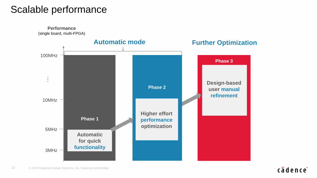
Scalable performance
5MHz
10MHz
100MHz
Automatic mode
Phase 1
3MHz
Performance(single board, multi-FPGA)
Automatic
for quick
functionality
Further Optimization
Phase 3
Design-based
user manual
refinement
…
Phase 2
Higher effort
performance
optimization

23 © 2018 Cadence Design Systems, Inc. Cadence confidential.
Scalable hardware
Single board
• 1 FPGA
• Up to 25M ASIC gates
• Affordable and scalable
• Highest performance
• Early software development
• IP verification
Single chassis system
• 2-8 FPGAs
• Up to 200M ASIC gates
• Flexible and scalable
• Fastest bring-up
• Unique SW debug capabilities
• Early software development
• HW/SW integration
Multi-chassis configuration
• 8-24 FPGAs
• Up to 600M ASIC gates
• Highest capacity
• Flexible use modes
• Advanced debug
• High performance regression
• Full system validation
Protium S1-G Protium S1-SC Protium S1-MC (2H 2017)

24 © 2018 Cadence Design Systems, Inc. Cadence confidential.
Palladium Z1 + Protium S1
Compile
RTL
Protium™ S1
• Highest performance
• SW development
• Regressions
Congruency and common environment
Palladium® Z1
• Best debug
• SoC integration & accel
• Rich use models
Speed &
SW development
Debug &
Rich use models

25 © 2018 Cadence Design Systems, Inc. Cadence confidential.
Protium S1 Fully Integrated Implementation Flow
• Automated prototyping flow
reduces time-to-prototype (TTP)
from months to weeks
• Design changes have much
lesser time impact on iterations
• Simpler single pass flow iterations
are run in hours not days
• Software development gets a
head start measured in months
not days
Months
1-2
days p
er
ite
ratio
n
Traditional FPGA-based
Prototyping Flow
ASIC RTL
(Verilog/VHDL/SV)
Prototype RTL
(Verilog/VHDL/SV)
TestFAIL
FPGA bit Files
FPGA Vendor
P&R
FPGA Partitioning
and Synthesis
Edit RTL
Probes
Waveforms
Independent re-run of
selected tests for debug
1-2
h p
er
ite
ratio
n
ASIC RTL
(Verilog/VHDL/SV)
FPGA Partitioning
and Synthesis
FPGA Vendor
P&R
Verification model
to validate FPGA
functionality
Optional
FPGA bit Files
Protium S1 FPGA-based
Prototyping Flow
Weeks
Functional
Assurance
Before P&R

26 © 2018 Cadence Design Systems, Inc. Cadence confidential.
Case study: Microsemi

27 © 2018 Cadence Design Systems, Inc. Cadence confidential.
Case study: Microsemi (cont.)

28 © 2018 Cadence Design Systems, Inc. Cadence confidential.
Cadence SpeedBridge Adapter Solutions Palladium® Series
PCIe 4.0/3.0/2.0/1.1/1.0a
Ethernet 10/100, 1G, 10G, 40G
SATA
SAS USB 2.0 Host
Protium S1
USB 3.0/2.0/1.1 Device
Video/AudioData Streaming
HD interfaces

29 © 2018 Cadence Design Systems, Inc. Cadence confidential.
SpeedBridge Configuration Manager (SCM)
• Error injection during System-level test*
• The SpeedBridge™ Configuration Manager components– Hardware: SCM; Software/GUI: SpeedBridge view
• Benefits of Remote Configurability– Confirmation of setup and configuration
– A complete environment for remote monitoring & use
– Protocol specific debug and SpeedBridge information
– DIP switches, LED status
– Remote SpeedBridge reset capability
– Ability to monitor multiple SpeedBridges from a single GUI
*New! – (EA) capability available on some of the SpeedBridge adapters

31 © 2018 Cadence Design Systems, Inc. Cadence confidential.
Comprehensive portfolio of accessories and interfaces
• Please see datasheet for comprehensive list of what is natively supported.– https://www.cadence.com/content/dam/cadence-
www/global/en_US/documents/tools/system-design-verification/protium-s1-fpga-based-prototyping-platform-ds.pdf

32 © 2018 Cadence Design Systems, Inc. Cadence confidential.
Protium S1 – the Most Efficient Way to Prototype Your SoC
• Fast time-to-prototyping (months to 1-2 weeks)– No RTL changes
– Automatic partitioning/memory compilation
– Fully integrated FPGA place-and-route
• Scalable performance (3-100MHz)– From fully automatic to fully manual
– Advanced black-box methodology
• Advanced software debug– Memory upload/download
– Force and release
– Data Capture card
– Assertion checkers
– State read-back

33 © 2018 Cadence Design Systems, Inc. Cadence confidential.
Software
FPGA bit files
Integrated Compile
EngineHDL-ICE
for fast
compile
Partitio
ning
FPGA P&R
M
e
m
o
r
y
c
o
m
p
i
l
e
r
D
e
b
u
g
i
n
s
e
r
t
e
r
Board router
B
o
a
r
d
f
i
l
e
ASIC RTL
(Verilog / VHDL /
SV)
Debug
probes and
trigger
conditions
Multi-fabric
Compiler
Transaction
Interface
Accessories
SpeedBridges
Memory Cards
Memory Models
Hardware
25MG200MG
600MG
Protium S1 Prototyping SolutionIndustry’s first comprehensive, fully integrated solution

34 © 2018 Cadence Design Systems, Inc. Cadence confidential.
… and Xilinx Likes it Too
“The Cadence Protium S1 platform ensures scalability to hundreds of software developers at the earliest possible point during the development flow, and allows developers to focus on design validation and software development rather than prototype bring-up.
The common flow with the Cadence Palladium Z1 emulation platform enables a smooth transition from emulation to prototyping, which greatly improves productivity.”
Peter Ryser, Senior Director for System Software, Integration, and Validation, Xilinx
© 2018 Cadence Design Systems, Inc. All rights reserved worldwide. Cadence, the Cadence logo, and the other Cadence marks found at www.cadence.com/go/trademarks are trademarks or registered trademarks of
Cadence Design Systems, Inc. All other trademarks are the property of their respective owners.