Embed Size (px)
Citation preview

NV012-C
(FPD-Link III d realizer board)
Hardware specifications
The 2nd edition
Net Vision Co., Ltd.

Net Vision Co., Ltd.
NV012-C (FPD-Link III d realizer board) Hardware specifications The 2nd edition
2
Revision history
The
number
of
version
s
Date Content Charge
The 1st
edition
16/10/31 First edition creation (NV012-C) Yamada
The
2nd
edition
1705/23 Correction of a misprint Yamada

Net Vision Co., Ltd.
NV012-C (FPD-Link III d realizer board) Hardware specifications The 2nd edition
3
Table of contents
1.
Outline ............................................................................. 4
2.
Details ............................................................................. 6
2.1.
Power supply system ................................................................. 6
2.2.
I2C function ........................................................................ 7
2.3.
Connector table .................................................................... 7
2.4.
Details of a connector ................................................................ 9
2.5.
DIP switch setup ................................................................... 13
2.6.
LED indicator ..................................................................... 13
2.7.
HSD power supply polarity selection jumper ............................................. 14
3.
The procedure used .................................................................. 14
4.
Main specifications .................................................................. 15
5.
Appendix .......................................................................... 16
5.1.
Substrate dimensional drawing ........................................................ 16
5.2.
4 Wiring Diagram in CH Synchronous Taking-in System .................................. 17

Net Vision Co., Ltd.
NV012-C (FPD-Link III d realizer board) Hardware specifications The 2nd edition
4
1. Outline
These specifications are hardware specifications of NV012-C (FPD-Link III d realizer board).
NV012-C (a following book board and the notation) is a conversion board for changing into a parallel
signal the image of the serial signal transmitted by the TI, Inc. FPD-Link III standard, and using it,
connecting with SV series (SVM-03/03 U/SVI-06 etc.) of our company.
[Fig. 1] Block diagram
The block diagram of this substrate is shown in [Fig. 1]. This substrate carries TI, Inc. デシリアライ
ザ IC DS90UB914 A-Q1, Serial - parallel conversion of the FPD-Link III picture signal to the 100
MHz of maximum pixel clock and the I2C communication through a FPD-Link III signal wire are
possible. The output connector of the parallel signal serves as an interface common to SV series, and
SV board and the use linked directly are possible. The connector of a FAKRA standard is used for the
input of a serial signal (single-ended transmission), and it is ideal for connection with the camera of
an in-vehicle use.
It is this substrate and SVM-03 to [Fig. 3]. The board connection image of a substrate is shown.
As shown in a figure, both substrates are connected through the pin socket (CN2) of 50 pins. Since a
screw hole position is common to both boards, it can fix both substrates by a spacer etc. The
arrangement plan of the connector of this substrate is as being shown in [Fig. 4]. The clause of "the
details of a connector" shows the pin number of a connector, and pin assignment later.

Net Vision Co., Ltd.
NV012-C (FPD-Link III d realizer board) Hardware specifications The 2nd edition
5
[Fig. 3] Board connection image
[Fig. 4] Connector arrangement plan
* CN4, CN6, CN7, and CN11 are un-mounting.

Net Vision Co., Ltd.
NV012-C (FPD-Link III d realizer board) Hardware specifications The 2nd edition
6
2. Details
2.1. Power supply system
1.8V regulator (LDO) is carried in this substrate, and this supplies the power supply to the core
voltage of デシリアライザ IC. Power supply (core voltage, IO voltage) of IC It supplies from SV
board of SVM-03 etc. through connector CN2. At this time, VDDH and VDDL of SV board correspond
to the core voltage and IO voltage of this substrate, respectively. Usually, both VDDH and VDDL are
set as 3.3V.
Moreover, in this substrate, the power supply for cameras can be superimposed on a FPD-Link III
cable. This power supply is supplied from CN5, CN6, or CN8. Since the power supply for cameras
and IC are divided in direct current through the capacitor, an injection order of the power supply of
IC and the power supply for cameras is not asked.
The block diagram of the electric power system of this substrate is shown in [Fig. 5]. When using
DC jack (CN6) which connects an AC/DC adaptor, in this substrate, in preparation for future
extension, the pattern of DC converter in which 12V input is possible is prepared, and voltage is
changed by jumper resistance mounted on the substrate. With NV012-C Since the jumper is set to
the DC jack side, a camera power supply can be supplied via DC jack by mounting CN6.
[Fig. 5] Electric power system block diagram

Net Vision Co., Ltd.
NV012-C (FPD-Link III d realizer board) Hardware specifications The 2nd edition
7
2.2. I2C function
デシリアライザ IC (DS90UB914A) of this substrate has I2 C bus, and has an I2C communication
function with Syria Liza and the target device which let the setting change in IC, and a FPD-Link III
cable pass. In this substrate, since the pull-up of the I2 C bus of DS90UB914A was carried out to IO
voltage by 4.7 komega and also it is directly linked with the connector for SV series, I2C
communication is possible for it by the standard function of SV series as it is. Simultaneously, since
I2 C bus is directly linked with the I2C input and output connectors (CN4) on a substrate, connection
with an external device and the operation from an external master are also attained.
At this substrate, the I2C address of DS90UB914A is 2 by a DIP switch (SW1). Kind change is
possible. For details, please refer to the clause of a DIP switch setup.
2.3. Connector table
(Also pin map)
CN# Mounting
state
Name Part number
CN1 FPD-Link Input
(FAKRA Same axle)
FA1-NCRP-PCB-8
CN2 Parallel output C-00086
CN3 Unmounted (intact) N/A
CN4 Unmounted I2C Input and
output
171825-4
CN5 Camera power supply
input 1
22-04-1021
CN6 Unmounted Camera power supply
input 2
MJ-179P
Center +
CN7 Unmounted Extended connector 1 90130-1212
CN8 Camera power supply
input 3
171825-4
CN9 Extended connector 2 171825-6
CN10 FPD-Link Input
(HSD Differential)
D4S20L-40MA5-B
CN11 Unmounted (intact) N/A
* Apply a mounting state to NV012-C.
A camera power supply input connector (CN5, CN6, CN8) inputs DC power supply supplied to a

Net Vision Co., Ltd.
NV012-C (FPD-Link III d realizer board) Hardware specifications The 2nd edition
8
target device (camera) if needed. Please input a power supply from one of connectors according to
application or a system. This camera power supply is superimposed by the FPD-Link signal wire
when using CN1, and when using CN10, it is outputted to a specific pin. Moreover, a camera power
supply is not used inside a NV012-C board, but is supplied only to a target device. Required power
supply capacity is dependent on the characteristic of a target device.
Extended connectors (CN7, CN9) are the communication between substrates by a multi-channel
taking-in system, and a connector for future extension. I2C input and output connectors (CN4) are
directly linked with I2 C bus of DS90UB914A.

Net Vision Co., Ltd.
NV012-C (FPD-Link III d realizer board) Hardware specifications The 2nd edition
9
2.4. Details of a connector
Below, the upper surface figure (outline) of the connector of this substrate and pin assignment (an
extract is made from a circuit diagram) are shown.
(Pin assignment introductory notes)
Name Meaning
VDDIO IO Power supply
VCAM The power supply for cameras
VDDH SV VDDH of a board (CN2 direct connection)
SCL / SDA I2C Signal wire
P0 - P5 SV Wide use IO of a board Port (CN2 direct
connection)
PC_A/PC_K Reservation
(photocoupler 1 Intact in following side LED and
NV012-C)
- CN1 (FA1-NCRP-PCB-8)
(It connects with a circuit diagram and RIN1+)
- CN2 (the C-00086 = following figure right), CN3 (the following figure left)
(Figure seen from the substrate upper surface at the time of mounting)
* Pin assignment is referring to the hardware specifications of SV series.

Net Vision Co., Ltd.
NV012-C (FPD-Link III d realizer board) Hardware specifications The 2nd edition
10
- CN4 (171825-4 / TE Connectivity)
(Upper surface figure)
(Circuit diagram)
- CN5 (22-04-1021 / Molex), CN6 (MJ-179P / Marushin), CN8 (171825-4 / TE Connectivity)
(CN5 upper-surface figure)
(Circuit diagram)
(CN8 upper-surface figure)
- CN7 (90130-1212 / Molex)

Net Vision Co., Ltd.
NV012-C (FPD-Link III d realizer board) Hardware specifications The 2nd edition
11
(Upper surface figure)
(Circuit diagram)
- CN9 (171825-6 / TE Connectivity)
(Upper surface figure)
(Circuit diagram)
- CN10 (D4S20L-40-MA5-B /Rosenberger)
(Upper surface figure)

Net Vision Co., Ltd.
NV012-C (FPD-Link III d realizer board) Hardware specifications The 2nd edition
12
(Circuit diagram)
Net Vision Co., Ltd.
NV012-C (FPD-Link III d realizer board) Hardware specifications The 2nd edition
13
2.5. DIP switch setup
The DIP switch (SW1) of 8 bit is mounted in this substrate, and a デシリアライザ function, an I2C
address, etc. can be set up.
SW# Name Function
1 IDX0 I2C of DS90UB914A An address is specified.
ON: I2C Address = 0x60
OFF: I2C Address = 0x61
2 OSS_SEL An output state is chosen when a parallel output is effective.
ON: Hi-Z Output
OFF: an output -- effective
3 SEL An input connector is specified.
ON: Difference input (CN10:HSD it inputs from a connector)
OFF: Coaxial input (CN1:FAKRA it inputs from a connector)
4 BISTEN BIST (Built In Self Test) Mode is set up.
ON: BIST Mode Invalid
OFF: BIST Mode Effective
5 PDB Power down mode is set up.
ON: Power down
OFF: Normal operation
6 MODE0 Device mode is chosen.
Each details in the mode are DS90UB914A data sheet references.
MODE0 | MODE1 | MODE 2 |
ON | OFF | OFF | 10-bit Mode
OFF | ON | OFF | 12-bit High Frequency Mode
OFF | OFF | ON | 12-bit Low Frequency Mode
7 MODE1
8 MODE2
- A default is BISTEN. (4) and MODE0 Only (6) is ON.
2.6. LED indicator
Three LED is mounted in this substrate. Each function is as follows.
LED# Name Function
D2 PASS The light is switched on if the transmission error has not occurred.
D3 LOCK The light will be switched on if PLL locks.
D4 POWER The light will be switched on if the power supply (VDDH) is
supplied.

Net Vision Co., Ltd.
NV012-C (FPD-Link III d realizer board) Hardware specifications The 2nd edition
14
2.7. HSD power supply polarity selection jumper
JP3 and JP4 are the jumpers which choose the power supply output polarity of a HSD connector.
When performing the power supply output to the target which let the HSD connector pass, a passage
sets up a jumper below.
The output to HSD Jumper setup
Pin 1: GND
Pin 3: GND
(with no power
supply output)
JP3: 2-3 Between short circuit JP4: 2-3 Between short circuit
Pin 1: VCAM
Pin 3: GND
JP3: 1-2 Between short circuit JP4: 2-3 Between short circuit
Pin 1: GND
Pin 3: VCAM
JP3: 2-3 Between short circuit JP4: 1-2 Between short circuit
3. The procedure used
It is this substrate below SVM-03 The procedure used in the case of using it for a board, connecting is
explained.
- DIP SW of this substrate checks that it is a proper setup.
- Check that the target power supply (VDDH, VDDL) of SVM-03 is set to 3.3V.
- Connect this substrate with SVM-03.
- Insert a USB cable in SVM-03 and connect with PC.
- Check that the power supply indicator (D4) of this substrate is on.
- Connect a camera to CN1.
- Supply a camera power supply from CN5 or CN8.
The setup of this substrate is completed above. Since it is the same as the case where a camera is
connected to SVM-03, please follow the directions for SVM-03 henceforth.

Net Vision Co., Ltd.
NV012-C (FPD-Link III d realizer board) Hardware specifications The 2nd edition
15
4. Main specifications
Item Value Remarks
Substrate size 60.0 x 101.6 mm The value which does not contain a
connector
The power supply for
デシリアライザ
DC+3.3V±5% CN2 Capture boards, such as a course and
SVM-03U
It supplies from (VDDH).
IO Power supply DC +3.3V / 2.8V
±5%
CN2 Capture boards, such as a course and
SVM-03U
It supplies from (VDDL).
The power supply for
cameras
N/A (DC+5-9V grade) It supplies from CN5 or CN8 connector.
CN6 It is AC by mounting. It corresponds to
an adapter.
Power supply voltage follows a camera.
Image input FPD-Link III Standard A single end (FAKRA connector) or
differential (HSD connector)
Picture output Parallel signal
Maximum 75 MHz / 12bit
100MHz / 10bit
Interfaces are our company SV series
standards, such as SVM-03.
* The above-mentioned specification is applied only to part number NV012-C.
Net Vision Co., Ltd.
NV012-C (FPD-Link III d realizer board) Hardware specifications The 2nd edition
16
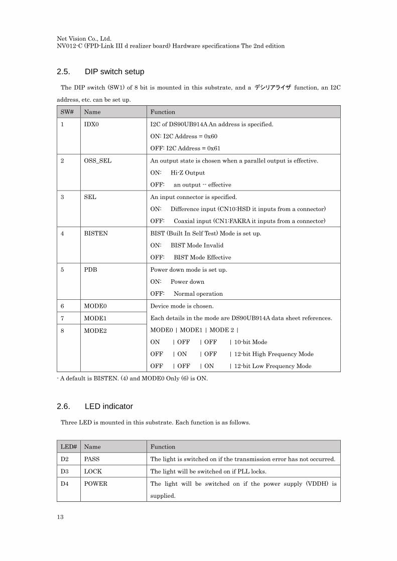
5. Appendix
5.1. Substrate dimensional drawing
(a copy article page/copy article page -- seeing)

Net Vision Co., Ltd.
NV012-C (FPD-Link III d realizer board) Hardware specifications The 2nd edition
17
(A solder side / 部品面視)
5.2. 4 Wiring Diagram in CH Synchronous Taking-in System
The following is reference data.