Embed Size (px)
Citation preview
Reg. Office:Saab Ericsson Space AB Telephone: Linköping Office: Telephone:
S-405 15 Göteborg +46 31 35 00 00 Saab Ericsson Space AB +46 13 28 64 00Sweden Telefax: S-581 88 Linköping Telefax:Reg. No: 556134-2204 +46 31 35 95 20 Sweden +46 13 13 16 28
Document NoMCD/SPC/0009/SEDate Issue Page10 Apr 1997 4 1/82 + 50
PROJECT
32 BIT MICROPROCESSOR AND COMPUTERSYSTEM DEVELOPMENT
TITLE
MEC REV. A DEVICE SPECIFICATION
Name Function Date Signature
Prepared : Mikael Ramström Project Engineer
Checked : Bo Törnberg Design Engineer
Authorized : Ritva Svenningsson Project Manager
DistributionComplete : ESTEC/5, MHS, LOGICA, SPACEBEL, ALSYS,
B2S, CK-MR, CK-MW, CM-DM, CM-BT/2, CM-JO, CM-TS, CSSummary :
Page : 2
The ownership and copyright of this document belong to Saab Ericsson Space AB and it must not be disclosed,copied, altered or used without the written permission of Saab Ericsson Space AB.
© Saab Ericsson Space AB
Document No : MCD/SPC/0009/SE Date : 10 Apr 1997 Issue : 4
DOCUMENT CHANGE RECORD
Changes between issues are marked with a left-bar.
Issue Date Paragraphs affected Change information
1 29 Feb 1996 All New document based on MCD/SPC/0005/SE,issue 8. Apart from the design changes betweenpreliminary MEC and MEC Revision A, thedocument has been reworked such that all trade-offand system discussion topics have been removed.These topics are instead addressed in anotherdocument; ERC32 System Overview.
2 23 April 1996 3.2, 3.6, 3.9, 3.16, 3.17, 3.18,3.19, 3.21.2, 4 and all TimingDiagrams
Updated after final design specification of Rev.A
3 28 Jan 1997 All Updated after El. characterisation andVHDL timing simulations of Rev.A
4 10 Apr 1997 3.2.6, table 33.21.2,4.1, table 6,Appendix 1
Typo error memory mapTypo error in I/O configuration registerTypo error in signals listTiming parameters updated:
t17 (max) was 15ns is 20nst19 (min) was 0ns to SYSCLK+
is 20ns to SYSCLK-t25 (max) was 15ns is 20nst26 (max) was 15ns is 20nst27 (max) was 15ns is 20nst55 (min) was 1000ns is 100nst55 (max) is 1000ns
Class : Industrial Host System : Word 2.0c for Windows, SE Macro Rev 2.2Contract No : Host File : \\NTSRV1\Arkiv1\mcd\spc\0009_04\0009_04.DOC
SUMMARY
This document constitutes a functional specification of iteration two of the MemoryController (MEC Revision A) which is an element in the ERC32 microprocessor core.It is intended to function as a User's guide both for the software and hardwaredevelopers.
Page : 3
The ownership and copyright of this document belong to Saab Ericsson Space AB and it must not be disclosed,copied, altered or used without the written permission of Saab Ericsson Space AB.
© Saab Ericsson Space AB
Document No : MCD/SPC/0009/SE Date : 10 Apr 1997 Issue : 4
TABLE OF CONTENTS Page
1. INTRODUCTION................................ ................................ .................... 51.1. Scope ................................ ................................ ................................ ..... 51.2. Documents................................ ................................ ............................. 61.2.1. Applicable Documents................................ ................................ .......... 61.2.2. Reference Documents................................ ................................ ........... 61.3. Glossary................................ ................................ ................................ . 71.4. Definitions................................ ................................ .............................. 81.4.1. Bit Numbering................................ ................................ ...................... 81.4.2. Signal Names................................ ................................ ....................... 81.4.3. Registers ................................ ................................ .............................. 8
2. GENERAL OVERVIEW OF ERC32................................ ....................... 92.1. ERC32 Overview................................ ................................ ................... 9
3. MEMORY CONTROLLER FUNCTIONS................................ ............. 113.1. Data Types................................ ................................ ........................... 133.2. Memory Interface................................ ................................ ................. 133.2.1. Memory Control Signals................................ ................................ ..... 133.2.2. RAM................................ ................................ ................................ .. 133.2.2.1. Extended RAM................................ ................................ ................ 143.2.3. Boot PROM................................ ................................ ....................... 153.2.3.1. Extended PROM................................ ................................ .............. 153.2.4. Exchange Memory................................ ................................ ............. 163.2.5. I/O ................................ ................................ ................................ ..... 163.2.5.1. Extended I/O ................................ ................................ ................... 183.2.6. MEC Memory Map................................ ................................ ............ 193.3. DMA Interface................................ ................................ ..................... 203.4. Bus Arbiter................................ ................................ ........................... 213.5. Execution Modes................................ ................................ .................. 213.5.1. Reset Mode................................ ................................ ........................ 233.5.2. Run Mode................................ ................................ .......................... 233.5.3. System Halt Mode................................ ................................ .............. 233.5.4. Power-Down Mode................................ ................................ ............ 243.5.5. Error Halt Mode................................ ................................ ................. 243.6. Wait-State and Timeout Generator................................ ....................... 243.7. Memory Access Protection................................ ................................ ... 253.7.1. Unimplemented Areas................................ ................................ ........ 253.7.2. RAM Write Access Protection................................ ............................ 263.7.3. Boot PROM Write Protection ................................ ............................ 273.8. Register Access Protection................................ ................................ ... 273.9. EDAC ................................ ................................ ................................ .. 283.9.1. Check Bit Generator................................ ................................ ........... 293.9.2. Syndrome Generator................................ ................................ .......... 30
Page : 4
The ownership and copyright of this document belong to Saab Ericsson Space AB and it must not be disclosed,copied, altered or used without the written permission of Saab Ericsson Space AB.
© Saab Ericsson Space AB
Document No : MCD/SPC/0009/SE Date : 10 Apr 1997 Issue : 4
3.9.3. Syndrome Detector ................................ ................................ ............ 313.9.4. Fault Injection................................ ................................ .................... 323.9.5. Memory and I/O Parity................................ ................................ ....... 323.10. Memory Redundancy................................ ................................ ............ 333.11. Synchronous Traps................................ ................................ ............... 333.12. Interrupts (Asynchronous Traps)................................ .......................... 343.13. General Purpose and Real Time Clock Timers................................ ...... 373.14. Watch Dog................................ ................................ ........................... 393.15. UART ................................ ................................ ................................ .. 413.16. Parity Checking................................ ................................ .................... 423.17. Error Handler ................................ ................................ ....................... 433.18. System Availability................................ ................................ ............... 473.19. Test mode and Test Access Port................................ ........................... 473.19.1. EDAC Test ................................ ................................ ........................ 473.19.2. Parity Test................................ ................................ .......................... 473.19.3. Interrupt Test ................................ ................................ ..................... 473.19.4. Error Test ................................ ................................ .......................... 483.19.5. Test Access Port (TAP)................................ ................................ ...... 483.20. System Clock................................ ................................ ....................... 483.21. MEC Registers................................ ................................ ..................... 493.21.1. Register Address Map................................ ................................ ........ 493.21.2. Register Configuration and Bit Allocation................................ ........... 50
4. MEMORY CONTROLLER SIGNAL DESCRIPTIONS........................ 634.1. Memory Controller Signal Summary................................ ..................... 634.2. MEC Detailed Signal Descriptions................................ ........................ 654.2.1. IU/FPU Interface Signals................................ ................................ .... 654.2.2. Memory System Interface Signals................................ ....................... 714.2.3. Interrupt and Control Signals................................ .............................. 754.2.4. Test Access Port Signals................................ ................................ .... 774.2.5. UART Interface ................................ ................................ ................. 784.2.6. Power and Clock Signals................................ ................................ .... 79
5. ELECTRICAL AND MECHANICAL SPECIFICATION....................... 805.1. Maximum Rating and DC Characteristics................................ .............. 805.1.1. Maximum Ratings................................ ................................ .............. 805.1.2. Operating Range................................ ................................ ................ 805.1.3. DC Characteristics over the Operating Range................................ ..... 805.1.4. Capacitance Ratings................................ ................................ ........... 815.2. Package Description................................ ................................ ............. 815.2.1. Pin Assignments................................ ................................ ................. 815.2.2. Package Diagram................................ ................................ ............... 82
Page : 5
The ownership and copyright of this document belong to Saab Ericsson Space AB and it must not be disclosed,copied, altered or used without the written permission of Saab Ericsson Space AB.
© Saab Ericsson Space AB
Document No : MCD/SPC/0009/SE Date : 10 Apr 1997 Issue : 4
1. INTRODUCTION
1.1. Scope
This document constitutes a functional specification of iteration two of the MemoryController (MEC Revision A) which is an element in the ERC32 microprocessor core. Itis intended to function as a User's guide both for the software and hardware developers.
The document is divided into the following sections:
• GENERAL OVERVIEW OF ERC32A short overview of a typical ERC32 based system.
• MEMORY CONTROLLER FUNCTIONSDetailed description of the MEC Revision A functions including software interface.
• MEMORY CONTROLLER SIGNAL DESCRIPTIONSFunctional description of MEC Revision A signals.
• ELECTRICAL AND MECHANICAL SPECIFICATION
• TIMING DIAGRAMS (APPENDIX 1)Timing specifications and diagrams.
Page : 6
The ownership and copyright of this document belong to Saab Ericsson Space AB and it must not be disclosed,copied, altered or used without the written permission of Saab Ericsson Space AB.
© Saab Ericsson Space AB
Document No : MCD/SPC/0009/SE Date : 10 Apr 1997 Issue : 4
1.2. Documents
1.2.1. Applicable Documents
AD1 ESA 32-Bit Microprocessor and Computer Development ProgrammeStatement of Work, WDI/JG/1317/NL, Issue 2.1, 28-05-1991.
AD2 Specification for a 32-bit embedded computing core (ERC32),WDI/JG/1334/NL, Issue 3, 29-05-1991.
AD3 32-bit Microprocessor Software Tools Technical Requirements,WDI/1339/FGM/NL, 05-06-1991.
AD4 ERC32 Technical Specification, MCD/SPC/0001/SE, issue 7, 1 Apr 1994.
1.2.2. Reference Documents
RD1 SPARC Standard Version 7
RD2 IU-RT Preliminary Device Specification, AMS/IURT/0017/CLG, issue 6,August 28th 1995.
RD3 FPU-RT Preliminary Device Specification, AMS/FPURT/0018/VS, issue 6,August 28th 1995.
RD4 MEC Device Specification, MCD/SPC/0005/SE, issue 8December 1st 1995.
Page : 7
The ownership and copyright of this document belong to Saab Ericsson Space AB and it must not be disclosed,copied, altered or used without the written permission of Saab Ericsson Space AB.
© Saab Ericsson Space AB
Document No : MCD/SPC/0009/SE Date : 10 Apr 1997 Issue : 4
1.3. Glossary
AD Applicable DocumentASI Address Space IdentifierATAC Ada TAsking CoprocessorCS Chip SelectDMA Direct Memory AccessEDAC Error Detection And CorrectionEEPROM Electrically Erasable Programmable Read Only MemoryERC32 32 bit Embedded Real-time Computing CoreEXM EXchange MemoryFAR Failing Address RegisterFPU Floating Point UnitI/O Input/OutputICR Interrupt Clear RegisterIFR Interrupt Force RegisterIMR Interrupt Mask RegisterIPR Interrupt Pending RegisterIU Integer UnitMEC MEmory ControllerPROM Programmable Read Only MemoryRAM Random Access MemoryRD Reference DocumentROM Read Only MemoryRTC Real Time ClockSFSRSystem Fault Status RegisterSW SoftwareTAP Test Access PortTBC To Be ConfirmedTBD To Be DefinedUART Universal Asynchronous Receiver TransmitterWD Watch Dog
Page : 8
The ownership and copyright of this document belong to Saab Ericsson Space AB and it must not be disclosed,copied, altered or used without the written permission of Saab Ericsson Space AB.
© Saab Ericsson Space AB
Document No : MCD/SPC/0009/SE Date : 10 Apr 1997 Issue : 4
1.4. Definitions
1.4.1. Bit Numbering
In this document the following conventions are used:
- The most significant bit in a vector has the highest bit number and the leftmostposition in a field.
- The least significant bit in a vector has the lowest bit number and the rightmostposition in a field.
1.4.2. Signal Names
The following conventions are used for signal names:
- Signal names are written in capital letters, SIGNALNAME.- Active low signals are named, SIGNALNAME*.
1.4.3. Registers
The following convention is used for registers.
- Register names are bolded, Register Name.
Page : 9
The ownership and copyright of this document belong to Saab Ericsson Space AB and it must not be disclosed,copied, altered or used without the written permission of Saab Ericsson Space AB.
© Saab Ericsson Space AB
Document No : MCD/SPC/0009/SE Date : 10 Apr 1997 Issue : 4
2. GENERAL OVERVIEW OF ERC32
2.1. ERC32 Overview
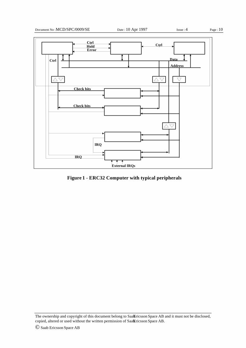
The objective of the ERC32 is to provide a high performance 32-bit computing core foron-board embedded real-time computers. The core is characterized by low circuitcomplexity and power consumption. Extensive concurrent error detection and supportfor fault-tolerance and reconfiguration is emphasized.
In addition to the main objective, the ERC32 core is possible to use for performancedemanding research applications in deep space probes. In addition to the abovecharacteristics the radiation tolerance and error masking are important. By includingsupport for reconfigurable of the error handling the different demands from theapplications can be optimized for the best purpose in each case.
The ERC32 is to be used as a building block only requiring memory and applicationspecific peripherals to be added to form a complete on-board computer. All other systemsupport functions are provided by the core.
The ERC32 incorporates the followings functions:
- Processor, which consists of one Integer Unit (IU) and one Floating Point Unit(FPU). The processor includes concurrent error detection facilities.
- Memory Controller (MEC), which is a unit consisting of all necessary supportfunctions such as memory control and protection, EDAC, wait state generator,timers, interrupt handler, watch dog, UARTs, and test support. The unit alsoincludes concurrent error detection facilities.
- One or two oscillator(s).
- Buffers necessary to interface with memory and peripherals.
Figure 1 schematically shows a basic ERC32 computer with external functions added toform a complete system.
Page : 10
The ownership and copyright of this document belong to Saab Ericsson Space AB and it must not be disclosed,copied, altered or used without the written permission of Saab Ericsson Space AB.
© Saab Ericsson Space AB
Document No : MCD/SPC/0009/SE Date : 10 Apr 1997 Issue : 4
CtrlHoldError
Ctrl
Ctrl
Check bits
IRQ
IRQ
External IRQs
Data
Address
Check bits
Figure 1 - ERC32 Computer with typical peripherals
Page : 11
The ownership and copyright of this document belong to Saab Ericsson Space AB and it must not be disclosed,copied, altered or used without the written permission of Saab Ericsson Space AB.
© Saab Ericsson Space AB
Document No : MCD/SPC/0009/SE Date : 10 Apr 1997 Issue : 4
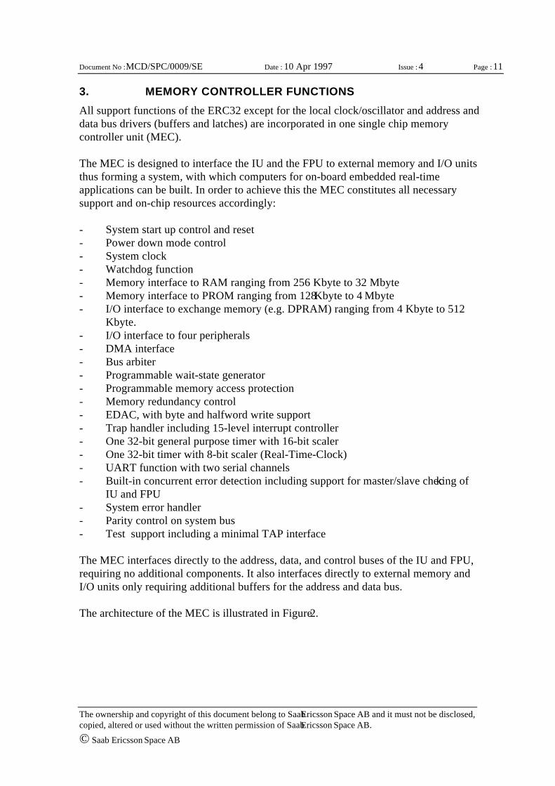
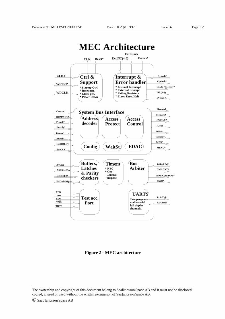
3. MEMORY CONTROLLER FUNCTIONS
All support functions of the ERC32 except for the local clock/oscillator and address anddata bus drivers (buffers and latches) are incorporated in one single chip memorycontroller unit (MEC).
The MEC is designed to interface the IU and the FPU to external memory and I/O unitsthus forming a system, with which computers for on-board embedded real-timeapplications can be built. In order to achieve this the MEC constitutes all necessarysupport and on-chip resources accordingly:
- System start up control and reset- Power down mode control- System clock- Watchdog function- Memory interface to RAM ranging from 256 Kbyte to 32 Mbyte- Memory interface to PROM ranging from 128 Kbyte to 4 Mbyte- I/O interface to exchange memory (e.g. DPRAM) ranging from 4 Kbyte to 512
Kbyte.- I/O interface to four peripherals- DMA interface- Bus arbiter- Programmable wait-state generator- Programmable memory access protection- Memory redundancy control- EDAC, with byte and halfword write support- Trap handler including 15-level interrupt controller- One 32-bit general purpose timer with 16-bit scaler- One 32-bit timer with 8-bit scaler (Real-Time-Clock)- UART function with two serial channels- Built-in concurrent error detection including support for master/slave checking of
IU and FPU- System error handler- Parity control on system bus- Test support including a minimal TAP interface
The MEC interfaces directly to the address, data, and control buses of the IU and FPU,requiring no additional components. It also interfaces directly to external memory andI/O units only requiring additional buffers for the address and data bus.
The architecture of the MEC is illustrated in Figure 2.
Page : 12
The ownership and copyright of this document belong to Saab Ericsson Space AB and it must not be disclosed,copied, altered or used without the written permission of Saab Ericsson Space AB.
© Saab Ericsson Space AB
Document No : MCD/SPC/0009/SE Date : 10 Apr 1997 Issue : 4
MEC Architecture
System Bus Interface
Ctrl &Support
Interrupt &Error handler
Addressdecoder
Access Protect
Access Control
Config WaitSt. EDAC
Buffers,Latches& Paritycheckers
Timers BusArbiter
Test acc.Port
UARTS
* Startup Ctrl* Reset gen.* Clock gen.* Power Down
* Internal Interrupt* External Iterrupt* Failing Registers* Error Reset/Halt
* RTC* One General purpose
Two program-mable serialfull duplex channels.
TRST
TMSTDOTDITCK
A/Apar
ASI/Size/Par
Data/Dpar
IMCtrl/IMpar
Control
ROMWRT*
Prom8*
Busrdy*
Buserr*
ExtHOLD*
CLK2
Sysreset*
WDCLK
CLK Reset* ExtINT(4:0) ExtIntack
Errors*
Syshalt*
Cpuhalt*
SysAv / MecErr*
IRL(3:0)
INTACK
Memctrl
MemCS*
ROMCS*
IOctrl
IOSel*
Mhold*
MDS*
MEXC*
DMAREQ*
DMAGNT*
AOE/COE/DOE*
Bhold*
TxA/TxB
RxA/RxB
NoPar*
ExtCCV
Figure 2 - MEC architecture
Page : 13
The ownership and copyright of this document belong to Saab Ericsson Space AB and it must not be disclosed,copied, altered or used without the written permission of Saab Ericsson Space AB.
© Saab Ericsson Space AB
Document No : MCD/SPC/0009/SE Date : 10 Apr 1997 Issue : 4
3.1. Data Types
Data type definitions follow the SPARC standard version 7. A byte is 8 bits wide, ahalfword is 16 bits wide, a word is 32 bits wide, and a double word is 64 bits wide.Organization and addressing of data in memory follow the "Big-Endian" conventionwherein lower addresses contain the high-order bytes. For a stored word, address Ncorresponds to the most significant byte and N+3 corresponds to the least significantbyte.
3.2. Memory Interface
3.2.1. Memory Control Signals
The MEC asserts a system address latch enable signal, ALE*, when the IU address orthe DMA address is valid. This signal is asserted once in every memory access cycle.
Four buffer enable signals are provided, RAMBEN*, ROMBEN*, MEMBEN* andIOBEN*. RAMBEN* is asserted during RAM access. ROMBEN* is asserted duringboot PROM access. MEMBEN* is asserted both during RAM and boot PROM access.IOBEN* is asserted during I/O, Extended general area and exchange memory access.
DDIR and DDIR* are output by the MEC to indicate buffer direction.
As RAM chip select signals MEMCS*(9:0) are provided. The boot PROM chip selectsignal is ROMCS*. Four I/O device chip select signals are provided, IOSEL(3:0).EXMCS* is used as chip select signal for exchange memory.
For RAM and boot PROM write access two strobe pairs are provided, MEMWR1*(1:0)and MEMWR2*(1:0). MEMWR1* is used to strobe data, D(31:0) into memory.MEMWR2* is used to strobe check bits, CB(6:0) and parity, DPARIO, into memory.
For I/O and exchange memory write access the IOWR* strobe is provided.
As output enable to memory during read access, OE*(1:0) is provided.
BUSRDY* is used to control access cycle length when accessing I/O, exchange memoryand extended areas.
BUSERR* is used to signal erroneous access to the MEC when accessing I/O, exchangememory and extended areas.
3.2.2. RAM
The MEC is reprogrammable to interface with a number of different RAM sizes andorganisations. The table below shows all possible memory sizes and organisations:
Page : 14
The ownership and copyright of this document belong to Saab Ericsson Space AB and it must not be disclosed,copied, altered or used without the written permission of Saab Ericsson Space AB.
© Saab Ericsson Space AB
Document No : MCD/SPC/0009/SE Date : 10 Apr 1997 Issue : 4
Selection of RAM size is performed by programming the Memory ConfigurationRegister (see page 52). The default value after system reset is 256 Kbytes.
It is possible to divide the selected RAM size into one, two, four, or eight equally sizedmemory blocks by programming the Memory Configuration Register. The default valueafter system reset is one block. A memory block is a block composed of 32-bit data,parity bit, and 7-bit check code and controlled with one chip select signal.
The MEC provides eight RAM memory chip selects. One, two, four, or eight chip selectsare possible to use corresponding to the programmed number of memory blocks. Thedefault value after system reset is one chip select. The MEC also provides two additionalRAM chip selects to handle memory redundancy. See paragraph 3.10.
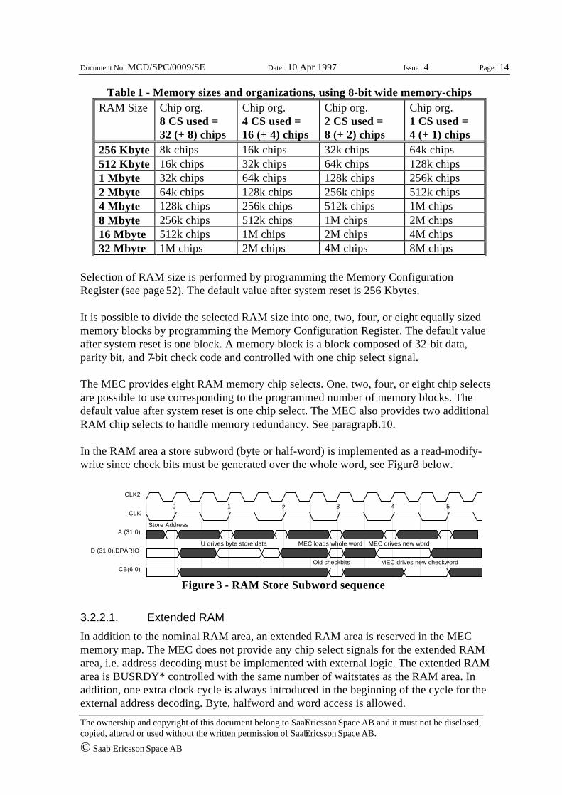
In the RAM area a store subword (byte or half-word) is implemented as a read-modify-write since check bits must be generated over the whole word, see Figure 3 below.
2 3 4 50 1
Store Address
IU drives byte store data
MEC drives new checkword
MEC loads whole word MEC drives new word
Old checkbits
CLK2
CLK
A (31:0)
D (31:0),DPARIO
CB(6:0)
Figure 3 - RAM Store Subword sequence
3.2.2.1. Extended RAM
In addition to the nominal RAM area, an extended RAM area is reserved in the MECmemory map. The MEC does not provide any chip select signals for the extended RAMarea, i.e. address decoding must be implemented with external logic. The extended RAMarea is BUSRDY* controlled with the same number of waitstates as the RAM area. Inaddition, one extra clock cycle is always introduced in the beginning of the cycle for theexternal address decoding. Byte, halfword and word access is allowed.
Table 1 - Memory sizes and organizations, using 8-bit wide memory-chipsRAM Size Chip org.
8 CS used =32 (+ 8) chips
Chip org.4 CS used =16 (+ 4) chips
Chip org.2 CS used =8 (+ 2) chips
Chip org.1 CS used =4 (+ 1) chips
256 Kbyte 8k chips 16k chips 32k chips 64k chips512 Kbyte 16k chips 32k chips 64k chips 128k chips1 Mbyte 32k chips 64k chips 128k chips 256k chips2 Mbyte 64k chips 128k chips 256k chips 512k chips4 Mbyte 128k chips 256k chips 512k chips 1M chips8 Mbyte 256k chips 512k chips 1M chips 2M chips16 Mbyte 512k chips 1M chips 2M chips 4M chips32 Mbyte 1M chips 2M chips 4M chips 8M chips
Page : 15
The ownership and copyright of this document belong to Saab Ericsson Space AB and it must not be disclosed,copied, altered or used without the written permission of Saab Ericsson Space AB.
© Saab Ericsson Space AB
Document No : MCD/SPC/0009/SE Date : 10 Apr 1997 Issue : 4
3.2.3. Boot PROM
The MEC allows software to be executed from a single byte-wide PROM. Alternatively,a full wide EDAC protected (40 bits) PROM can be used. Hereafter this start-up PROMis called boot PROM.
One extra clock cycle is always introduced in the beginning of the cycle for the addressdecoding. The IU supports byte operations on data, but for instruction fetches it needs afull 32 bit wide word. In the case that byte-wide boot PROM is used (selected byasserting the PROM8* input pin of the MEC), the MEC performs an 8 to 32 bitconversion of the boot PROM data during read access. This means that a word access tobyte-wide boot PROM will correspond to four byte fetches. The total number of cyclesrequired for each word read will then be equal to 4*(1+ no. of boot PROMwaitstates)+2.
When 32-bit wide PROM is used both EDAC and parity bits must be supplied to theMEC.
During read operations, byte, halfword and word access is allowed. If the boot PROM isbased on EEPROM devices, the MEC supports write access, but note that only bytewrite is supported if byte-wide EEPROM is used. The write access possibility is enabledby asserting the Prom Write Control signal (ROMWRT*).
The following sizes of the boot PROM are allowed: 128 Kbytes, 256 Kbytes,512 Kbytes, 1 Mbytes, 2 Mbytes, 4 Mbytes, 8 Mbytes and 16 Mbytes. Selection ofPROM size is to be performed by programming the Memory Configuration Register(see page 51). The default size of the boot PROM after system reset is the minimum size,128 Kbytes. The MEC provides one PROM chip select output.
3.2.3.1. Extended PROM
In addition to the boot PROM area, an extended PROM area is reserved in the MECmemory map. The MEC does not provide any chip select signals for the extended PROMarea, i.e. address decoding must be implemented with external logic. The extendedPROM area is BUSRDY* controlled with the same number of waitstates as the bootPROM area. In addition, one extra clock cycle is always introduced in the beginning ofthe cycle for the external address decoding. The number of cycles is however always atleast two even if the PROM area waitstate value has been programmed to zero. Thesame restrictions as for boot PROM apply regarding data width and write access.
3.2.4. Exchange Memory
The MEC supports a dedicated exchange memory area that can be used for system businterchange of data.
Page : 16
The ownership and copyright of this document belong to Saab Ericsson Space AB and it must not be disclosed,copied, altered or used without the written permission of Saab Ericsson Space AB.
© Saab Ericsson Space AB
Document No : MCD/SPC/0009/SE Date : 10 Apr 1997 Issue : 4
The following sizes of the exchange memory are allowed: 4 Kbytes, 8 Kbytes,16 Kbytes, 32 Kbytes, 64 Kbytes, 128 Kbytes, 256 Kbytes, and 512 Kbytes. Selection ofexchange memory size is done by programming the Memory Configuration Register(see page 52). The default value of the exchange memory size after system reset is theminimum size, 4 Kbytes. The MEC provides one exchange memory chip select output.
Only word access is allowed in the exchange memory area. Any attempt to access byteor halfword data in the exchange memory will cause a memory exception.
In case the exchange memory includes EDAC check bits and parity bits, these protectionbits will be treated in the same manner as for the main memory. If the exchange memorydoes not include any check bits, the MEC will generate the parity to the IU. The defaultis that no EDAC or parity is implemented in the exchange memory. If the exchangememory implements check bits, this must be defined in the Memory ConfigurationRegister in the MEC during start up and initialization.
The MEC is designed to allow implementation of the exchange memory with a DPRAM.The BUSY signal from the DPRAM can then be connected to the BUSRDY* signal ofthe MEC. The MEC waits one cycle at the start of the access for the assertion of theBUSRDY* signal. If the BUSRDY* signal is asserted in the beginning of the secondcycle, the normal data wait-state controlled access continues. If the BUSRDY* signal isdeasserted during the wait-states, the MEC will delay the access until the BUSRDY*signal has been asserted and then continue with the normal data wait-state controlledaccess. If a cycle is prolonged to more than 256 clock cycles, the Bus Timeout functionwill signal a system bus error.
The minimum length of an exchange memory access is three clock cycles.
3.2.5. I/O
Four address decoded I/O select outputs are provided in the MEC.
The minimum length of an I/O access for each I/O select is programmable in the MEC.The BUSRDY* signal is used to prolong I/O access for devices with variable accesstime. The BUSERR* signal is used to signal to the MEC that a bus error has occurred.
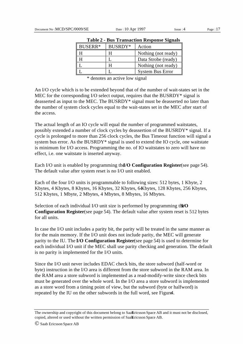
Table 2 gives the encoding for the system bus transaction response signals. Thetransactions that signal a system bus error, set the corresponding bit in the System FaultStatus Register (SFSR) of the MEC, which then responds by asserting Error to theinterrupt logic. These bits describe system bus error cases, in addition the bus timeout isset if the internal bus time out timer causes abortion.
Page : 17
The ownership and copyright of this document belong to Saab Ericsson Space AB and it must not be disclosed,copied, altered or used without the written permission of Saab Ericsson Space AB.
© Saab Ericsson Space AB
Document No : MCD/SPC/0009/SE Date : 10 Apr 1997 Issue : 4
An I/O cycle which is to be extended beyond that of the number of wait-states set in theMEC for the corresponding I/O select output, requires that the BUSRDY* signal isdeasserted as input to the MEC. The BUSRDY* signal must be deasserted no later thanthe number of system clock cycles equal to the wait-states set in the MEC after start ofthe access.
The actual length of an IO cycle will equal the number of programmed waitstates,possibly extended a number of clock cycles by deassertion of the BUSRDY* signal. If acycle is prolonged to more than 256 clock cycles, the Bus Timeout function will signal asystem bus error. As the BUSRDY* signal is used to extend the IO cycle, one waitstateis minimum for I/O access. Programming the no. of IO waitstates to zero will have noeffect, i.e. one waitstate is inserted anyway.
Each I/O unit is enabled by programming the I/O Configuration Register (see page 54).The default value after system reset is no I/O unit enabled.
Each of the four I/O units is programmable to following sizes: 512 bytes, 1 Kbyte, 2Kbytes, 4 Kbytes, 8 Kbytes, 16 Kbytes, 32 Kbytes, 64 Kbytes, 128 Kbytes, 256 Kbytes,512 Kbytes, 1 Mbyte, 2 Mbytes, 4 Mbytes, 8 Mbytes, 16 Mbytes.
Selection of each individual I/O unit size is performed by programming the I/OConfiguration Register (see page 54). The default value after system reset is 512 bytesfor all units.
In case the I/O unit includes a parity bit, the parity will be treated in the same manner asfor the main memory. If the I/O unit does not include parity, the MEC will generateparity to the IU. The I/O Configuration Register (see page 54) is used to determine foreach individual I/O unit if the MEC shall use parity checking and generation. The defaultis no parity is implemented for the I/O units.
Since the I/O unit never includes EDAC check bits, the store subword (half-word orbyte) instruction in the I/O area is different from the store subword in the RAM area. Inthe RAM area a store subword is implemented as a read-modify-write since check bitsmust be generated over the whole word. In the I/O area a store subword is implementedas a store word from a timing point of view, but the subword (byte or halfword) isrepeated by the IU on the other subwords in the full word, see Figure 4.
Table 2 - Bus Transaction Response SignalsBUSERR* BUSRDY* ActionH H Nothing (not ready)H L Data Strobe (ready)L H Nothing (not ready)L L System Bus Error
* denotes an active low signal

Page : 18
The ownership and copyright of this document belong to Saab Ericsson Space AB and it must not be disclosed,copied, altered or used without the written permission of Saab Ericsson Space AB.
© Saab Ericsson Space AB
Document No : MCD/SPC/0009/SE Date : 10 Apr 1997 Issue : 4
SAME DATA AS ON BITS(7:0)
SAME DATA AS ON BITS (15:0)
SAME DATA AS ON BITS(7:0)
SAME DATA AS ON BITS(7:0)
IU DATA
IU DATA
31 81624 0
DATA BIT
STORE BYTE
STORE HALF-WORD
Figure 4 - Store Subword Data Layout
3.2.5.1. Extended I/O
In addition to the nominal I/O area, an extended I/O area is reserved in the MECmemory map. The MEC does not provide any chip select signals for the extended I(Oarea, i.e. address decoding must be implemented with external logic. The extended I/Oarea is BUSRDY* controlled with the same number of waitstates as the nominal I/Oarea. The number of waitstates is however always at least one even if the I/O areawaitstate value has been programmed to zero. The same no. of waitstates and parityoption as for I/O area 3 apply.
Page : 19
The ownership and copyright of this document belong to Saab Ericsson Space AB and it must not be disclosed,copied, altered or used without the written permission of Saab Ericsson Space AB.
© Saab Ericsson Space AB
Document No : MCD/SPC/0009/SE Date : 10 Apr 1997 Issue : 4
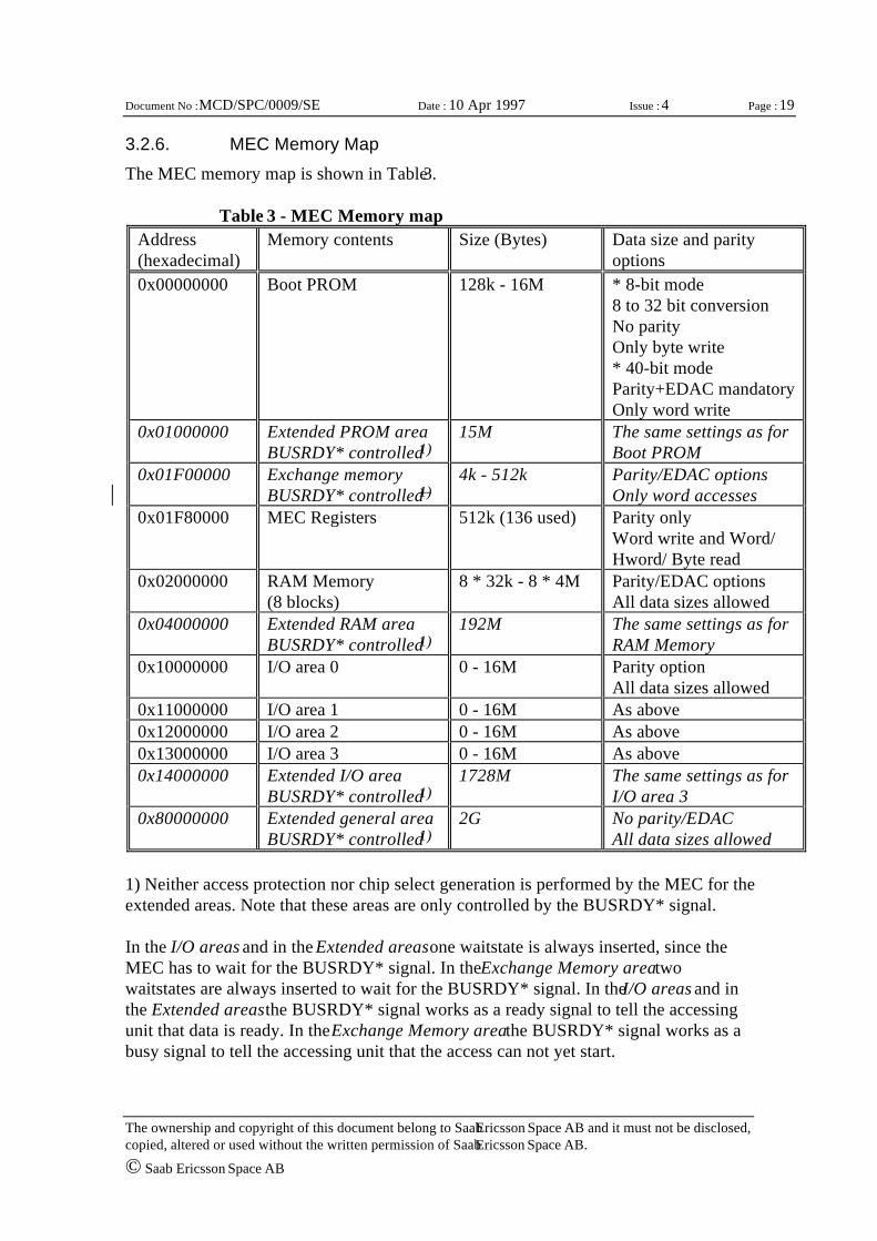
3.2.6. MEC Memory Map
The MEC memory map is shown in Table 3.
Table 3 - MEC Memory mapAddress(hexadecimal)
Memory contents Size (Bytes) Data size and parityoptions
0x00000000 Boot PROM 128k - 16M * 8-bit mode8 to 32 bit conversionNo parityOnly byte write* 40-bit modeParity+EDAC mandatoryOnly word write
0x01000000 Extended PROM areaBUSRDY* controlled1)
15M The same settings as forBoot PROM
0x01F00000 Exchange memoryBUSRDY* controlled1)
4k - 512k Parity/EDAC optionsOnly word accesses
0x01F80000 MEC Registers 512k (136 used) Parity onlyWord write and Word/Hword/ Byte read
0x02000000 RAM Memory(8 blocks)
8 * 32k - 8 * 4M Parity/EDAC optionsAll data sizes allowed
0x04000000 Extended RAM areaBUSRDY* controlled1)
192M The same settings as forRAM Memory
0x10000000 I/O area 0 0 - 16M Parity optionAll data sizes allowed
0x11000000 I/O area 1 0 - 16M As above0x12000000 I/O area 2 0 - 16M As above0x13000000 I/O area 3 0 - 16M As above0x14000000 Extended I/O area
BUSRDY* controlled1)1728M The same settings as for
I/O area 30x80000000 Extended general area
BUSRDY* controlled1)2G No parity/EDAC
All data sizes allowed
1) Neither access protection nor chip select generation is performed by the MEC for theextended areas. Note that these areas are only controlled by the BUSRDY* signal.
In the I/O areas and in the Extended areas one waitstate is always inserted, since theMEC has to wait for the BUSRDY* signal. In the Exchange Memory area twowaitstates are always inserted to wait for the BUSRDY* signal. In the I/O areas and inthe Extended areas the BUSRDY* signal works as a ready signal to tell the accessingunit that data is ready. In the Exchange Memory area the BUSRDY* signal works as abusy signal to tell the accessing unit that the access can not yet start.
Page : 20
The ownership and copyright of this document belong to Saab Ericsson Space AB and it must not be disclosed,copied, altered or used without the written permission of Saab Ericsson Space AB.
© Saab Ericsson Space AB
Document No : MCD/SPC/0009/SE Date : 10 Apr 1997 Issue : 4
3.3. DMA Interface
The MEC supports Direct Memory Access (DMA). The DMA unit requests access tothe processor bus by asserting the DMA request signal, DMAREQ*. When the DMAunit receives the DMAGNT* signal in response, the processor bus is granted. In case theprocessor is in the power down mode the IU is permanent three-stated, and aDMAREQ* will directly give a DMAGNT*. The detailed timing for DMA accesses isdefined in Appendix A.
It is possible to enable/disable DMA access to the system bus by programming the MECControl Register (see page 51). The default status after system reset is DMA enabled(i.e. permitted).
If DMA is enabled, the MEC asserts BHOLD* and deasserts AOE*, COE*, and DOE*following an DMA Request and then asserts DMA Grant.
A memory cycle started by the processor is not interrupted by a DMA access before it isfinished. The following signals shall be used by the DMA unit during the access:
- DMAREQ* to be generated by the DMA unit asking for access- DMAGNT* generated by the MEC when DMA access is granted- SYSCLK from the MEC to be used as synchronizing clock- A[31:0], ASI[3:0] address and SIZE[1:0], WRT, WE*, RD, DXFER,
LDSTO, LOCK to be generated by the DMA unit.- SIZE0 and SIZE1, to be driven by the DMA during DMA transfers. Note
that only word transfers are allowed in DMA mode, which means that thevalues of the size bits must always be driven to SIZE0 = 0 and SIZE1 = 1in DMA mode.
- APAR, ASPAR and IMPAR parity bits, to be generated by the DMA unitin case parity is enabled for the DMA
- D[31:0] data generated by the DMA unit in case of write cycle or fetchedby the DMA unit during read cycle
- DPARIO, data parity, to be generated and possibly checked by the DMAunit in case parity is enabled for the DMA
- DMAAS line used for address strobe to be generated by the DMA unitwhen the address is valid. Assertion of this signal will initiate the memoryaccess.
- DRDY* line used for indicating data ready for the DMA unit or datawritten on write. It is generated by the MEC
- MEXC* generated by the MEC indicating a memory access exceptionwhen no valid data can be supplied from the memory system, e.g. accessviolation or error.
If no subsequent DMA cycles are to be issued the DMA unit shall remove theDMAREQ* signal as soon as it has fetched the data on read after that it has received
Page : 21
The ownership and copyright of this document belong to Saab Ericsson Space AB and it must not be disclosed,copied, altered or used without the written permission of Saab Ericsson Space AB.
© Saab Ericsson Space AB
Document No : MCD/SPC/0009/SE Date : 10 Apr 1997 Issue : 4
DRDY*, or when DRDY* is removed on write. The MEC will then remove theDMAGNT* signal.
It is possible to enable/disable DMA parity by programming the MEC Control Register(see page 54). The default status after system reset is that DMA parity is disabled. IfDMA parity is enabled it has to be generated during write and possibly checked by theDMA during read. If DMA parity is not enabled the MEC generates the parity bit to bestored in the memory in case of write accesses.
Memory access protection is active also during DMA, i.e. attempted write access toprotected memory segments will lead to a memory exception, depending on how the ASIbits are driven by the DMA unit (user or supervisor mode).
Normally, the same restrictions apply to DMA access of MEC registers as for the IU inUser mode, see page 49. However during system halt (i.e. CPUHALT signal active), theDMA has the same access rights as the IU in supervisor mode for MEC register access.With register write access, memory protection could be changed to permit DMA toaccess all areas.
The MEC includes a DMA session timeout function preventing the DMA unit to lockoutthe IU/FPU by asserting DMAREQ* for a long time. If the DMA Request input is notdeasserted within 1024 system clock cycles after the assertion of DMA Grant, thememory exception output is asserted and the DMA Grant is removed. The DMA sessiontimeout function is possible to enable or disable by programming the MEC ControlRegister (see page 54). After system reset the timeout function is enabled.
Note that the DMA session timeout function is not the same as a bus timeout, rather ansession scheme timeout. In case of a bus timeout during DMA, the MEC asserts theMemory Exception output and removes the Bus Grant. For further actions taken seeparagraph 3.17.
3.4. Bus Arbiter
The IU and the FPU always have the lowest priority to the system bus and are deniedaccess to memory in case of a request from a DMA unit, unless the IU is performing alocked access or after a DMA exception cycle to allow interrupt handling.
Thus the DMA is granted access to the system bus provided this has been enabled by theIU in the MEC. In other words the IU has the capability to prevent DMA accesses bydisabling DMA in the MEC.
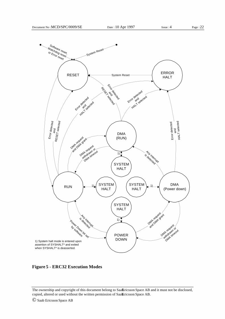
3.5. Execution Modes
The execution modes of the ERC32 as controlled by the MEC is shown in Figure 5.
Page : 22
The ownership and copyright of this document belong to Saab Ericsson Space AB and it must not be disclosed,copied, altered or used without the written permission of Saab Ericsson Space AB.
© Saab Ericsson Space AB
Document No : MCD/SPC/0009/SE Date : 10 Apr 1997 Issue : 4
1)
1)1)
1)
Software reset,
Watchdog reset
or Error reset
RESET ERRORHALT
RUN
POWERDOWN
Error d
etecte
d
and
HALT se
lected
Power Down bit set
by software
DMA(Power down)
DMA request
withdrawn or
DMA timeout
DMA requ
est
and D
MA gran
tAny interrupt
is detected
1) System halt mode is entered uponassertion of SYSHALT* and exitedwhen SYSHALT* is deasserted.
System Reset
System Reset
SYSTEMHALT
SYSTEMHALT
SYSTEMHALT
DMA(RUN)
SYSTEMHALT
DMA requ
est
and D
MA gran
t
DMA request
withdrawn or
DMA timeout Any interrupt
is detected
Error d
etected
and
HALT selecte
d
Err
or d
etec
ted
and
HA
LT s
elec
ted
Err
or d
etec
ted
and
RE
SE
T se
lect
ed
Error detected
and
RESET selected
Figure 5 - ERC32 Execution Modes
Page : 23
The ownership and copyright of this document belong to Saab Ericsson Space AB and it must not be disclosed,copied, altered or used without the written permission of Saab Ericsson Space AB.
© Saab Ericsson Space AB
Document No : MCD/SPC/0009/SE Date : 10 Apr 1997 Issue : 4
3.5.1. Reset Mode
When the SYSRES* input is asserted, the MEC issues a reset of itself and asserts theRESET* output which is intended be used as reset signal to all other components in thesystem (e.g. IU and FPU). The SYSRES* signal shall be applied for at least four clockcycles.
After the assertion of SYSRES*, the MEC starts the ERC32 system in the reset modewhich means that all MEC registers will be initialized to their reset contents.
The reset signal from the MEC to the IU/FPU etc., RESET*, is minimum 16 clockcycles long, i.e. it will remain asserted 16 system clock cycles after SYSRES* has beendeasserted.
Reset mode is also entered when the RESET* output of the MEC is asserted from anyother reason than SYSRES* :
• Software reset which is caused by the software writing to a Software ResetRegister (see page 51).
• Watchdog reset which is caused by a Watchdog counter timeout (see paragraph3.14.)
• Error reset which is caused by a hardware parity error, EDAC uncorrectable erroror a comparison error (see paragraph 3.17.)
When the reset cause is one of the above, all MEC registers will be initialized to theirreset contents except the Error and Reset Status Register (see page 61) whichcontains the source of the last processor reset (System reset, software reset, error reset,watch dog reset). By reading that register upon reset, the IU can determine the cause ofthe reset.
3.5.2. Run Mode
In this mode the IU/FPU is executing, all timers of the MEC are running (if softwareenabled) and the UART is running.
3.5.3. System Halt Mode
System Halt mode is entered when the SYSHALT* input of the MEC is asserted. TheCPUHALT* output is asserted, freezing IU/FPU execution. All timers are halted and theUART operation is stopped.
The MEC allows DMA accesses during system halt mode, in which DMA has permanentaccess to the system, i.e. DMAGNT* is asserted immediately on DMA request.
When SYSHALT* is deasserted, the previous mode is entered.
Page : 24
The ownership and copyright of this document belong to Saab Ericsson Space AB and it must not be disclosed,copied, altered or used without the written permission of Saab Ericsson Space AB.
© Saab Ericsson Space AB
Document No : MCD/SPC/0009/SE Date : 10 Apr 1997 Issue : 4
3.5.4. Power-Down Mode
This mode is entered by writing to the Power Down Register (see page 52) in the MEC,which will cause the MEC bus arbiter to remove the bus ownership from the IU. Theentering of power-down mode must first permitted by programming the MEC ControlRegister (see page 51).
In power-down mode the MEC asserts and maintains the BHOLD* and deasserts andmaintains the AOE*, COE*, and DOE* output signals. If an external interrupt isasserted whilst being in power down mode the MEC deasserts the BHOLD* and assertsthe AOE*, COE*, and DOE* output signals. And thereafter ensures that all data at allinputs to the IU/FPU are the same as it was before BHOLD* was asserted. The IU getsback the bus ownership and the MEC leaves the power-down mode.
The MEC allows DMA accesses during power-down mode, in which DMA haspermanent access to the system, i.e. DMAGNT* is asserted immediately on DMArequest.
3.5.5. Error Halt Mode
Error Halt mode is entered under the following circumstances:
• A hardware parity error, EDAC uncorrectable error or a comparison error (seeparagraph 3.17.) has occurred.
• The IU enters error mode (by asserting the ERROR* output)
In Error Halt mode, the CPUHALT* and SYSERR* outputs of the MEC are asserted(note that SYSERR* is also asserted if a masked error occurs even though Error Haltmode is not entered in this case). All timers are halted and the UART operation isstopped in this mode. The only way to exit Error Halt Mode is through Cold Reset byasserting SYSRES*.
The MEC allows DMA accesses during error halt mode, in which DMA has permanentaccess to the system, i.e. DMAGNT* is asserted immediately on DMA request.
Error Halt Mode can be induced by software by first setting the EWE bit in the TestControl Register (see page 61) and then write an error to the Error and Reset StatusRegister (see page 61). Note however that this also requires that the Reset/Halt bit forthe chosen error is set to halt in the MEC Control Register.
3.6. Wait-State and Timeout Generator
It is possible to control the wait state generation by programming a WaitstateConfiguration Register (see page 54) in the MEC. The maximum programmablenumber of wait-states is applied as default at reset.

Page : 25
The ownership and copyright of this document belong to Saab Ericsson Space AB and it must not be disclosed,copied, altered or used without the written permission of Saab Ericsson Space AB.
© Saab Ericsson Space AB
Document No : MCD/SPC/0009/SE Date : 10 Apr 1997 Issue : 4
It is possible to program the number of wait states for the following combinations:- RAM read- RAM write- PROM read- PROM write (i.e. EEPROM write)- ExM read/write (i.e. Exchange memory read/write)- Four individual I/O peripherals read/write
The MEC supports wait state generation by asserting the MHOLD* output in the secondmemory access cycle.
On exchange memory accesses the MEC will sense the bus ready signal (BUSRDY*)after the first two cycles of the access. If the bus ready signal is asserted at this time theMEC will continue with the programmed no. of wait states. However, if the bus readysignal is deasserted, the start of the access is put on hold. Once the bus ready signal isasserted again, the access will start with the programmed no. of waitstates.
On I/O and extended area accesses the MEC will sense the bus ready signal (BUSRDY*)after the first cycle of the access. If the bus ready signal is asserted at this time the MECwill continue with the programmed no. of wait states. If the bus ready signal isdeasserted at this time, the MEC will introduce wait states until the bus ready signal isagain asserted.
Note the difference between wait state handling for exchange memory and wait statehandling for I/O. For exchange memory, the access will start when BUSRDY* isasserted, i.e. after BUSRDY* is asserted an access with the programmed no. of waitstates will be performed. BUSRDY* is then handled as for the I/O and extended area.On the other hand, during I/O and extended area access, assertion of BUSRDY* signalsthe end of the access, i.e. the access will finish one cycle after BUSRDY* has beenasserted (at the earliest after the programmed no. of wait states).
A bus timeout function of 256 or 1024 system clock cycles is provided for the bus readycontrolled memory areas, 256 system clocks in the Extended RAM, Extended Generaland Extended I/O areas and 1024 system clocks in the Extended PROM area. The MECControl Register (see page 51) is used to select this function. The default after systemreset is that the bus timeout function is enabled.The bus timeout counter will start when the access is initiated. If the bus ready signal isnot asserted before a valid number of system clock cycles, a memory exception willoccur. For further actions taken see paragraph 3.17.
3.7. Memory Access Protection
3.7.1. Unimplemented Areas
Accesses to all unimplemented memory areas are handled by the MEC and detected asillegal, according to Table 3 (page 19). The memory and I/O configuration registers

Page : 26
The ownership and copyright of this document belong to Saab Ericsson Space AB and it must not be disclosed,copied, altered or used without the written permission of Saab Ericsson Space AB.
© Saab Ericsson Space AB
Document No : MCD/SPC/0009/SE Date : 10 Apr 1997 Issue : 4
define the size of memory and I/O areas. The unused area of the memory space,dependent on the programming of the memory size, is decoded as illegal.
If an access from the IU is attempted to an illegal area, the memory exception output isasserted. If an access from the DMA is attempted to an illegal area, the memoryexception output (MEXC*) and the DMA access error interrupt output are asserted.
For the extended areas no access protection is implemented. However, since these areasare bus ready( BUSRDY*) controlled the bus timeout function will detect an access toan unimplemented extended area.
When the IU issues the trap service routine, the contents of the MEC System FaultStatus Register (SFSR) give the cause of the exception.
When a memory data access violation error occurs (RAM write protection or illegalarea) the associated bus address is latched in a separate register, MEC Failing AddressRegister (FAR). With memory data access is meant IU operand fetch or DMA. An IUinstruction fetch error will not latch the bus address.
For further actions taken see paragraph 3.17.
3.7.2. RAM Write Access Protection
In addition to the access protection defined by the fixed memory map in the MEC whichwill detect any access to unimplemented and illegal addresses, the MEC can beprogrammed to detect and mask write accesses in any part of the RAM. The protectionscheme is enabled only for data area, not for the instruction area.
The programmable write access protection is segment based. A segment defines an areawhere write cycles are allowed. Any write cycle outside a segment is trapped and doesnot change the memory contents. Two segments are implemented. Each segment isimplemented with two registers: the Segment Base Register and the Segment EndRegister. The segment base register contains the start address of the segment, andenabling bits for supervisor/user mode (SE/UE). The segment end register contains thefirst address outside the segment, i.e. last address of segment plus one word. Only wordaligned addresses are supported. The segments are only active during RAM access, i.e.they can only be mapped to the RAM area.
If both the SE and UE bits of the Segment Base Register are cleared, write protection iseffectively disabled for that segment.
The segment access protection can also be used as a block protect function by setting theBP bit in the MEC Control Register. The BP bit inverts the address criterion for theprotection function so that any access within the segment is detected.
Page : 27
The ownership and copyright of this document belong to Saab Ericsson Space AB and it must not be disclosed,copied, altered or used without the written permission of Saab Ericsson Space AB.
© Saab Ericsson Space AB
Document No : MCD/SPC/0009/SE Date : 10 Apr 1997 Issue : 4
If a write access protection error is detected a memory exception is generated and theSFSR and Failing Address Register is updated as for unimplemented area accesses, seealso paragraph 3.17.
In normal mode, (BP=0), a memory exception is generated only if both segmentsindicated a write protection error. In block protect mode (BP=1), a memory exception isgenerated if any of the segments indicate a write protection error.
3.7.3. Boot PROM Write Protection
The MEC supports PROM write only when it is qualified by the external enable signalROMWRT and the enable bit in the Memory Configuration Register (see page 52).The MEC only supports byte write operations for an 8-bit wide PROM and only wordwrite operations for a 40-bit wide PROM.
If a write access to PROM is attempted when any of the above conditions are notfulfilled, the SFSR and Failing Address Register is updated as for unimplemented areaaccesses, see also paragraph 3.17.
3.8. Register Access Protection
All MEC registers except the UART RX and TX registers are readable in all accessmodes: user, supervisor, and DMA. The UART RX and TX registers are only readablein supervisor mode. The MEC allows word, halfword and byte accesses when a registeris read. The total 32-bit data (together with the parity bit) are thus always issued on thedata bus.
All MEC registers which are writeable, are writeable only in supervisor mode or in DMAmode if the CPUHALT* is active and only as full 32-bit size data write accesses to theregisters.
If a register access violation is performed by the IU, the memory exception output isasserted. If a register access violation is performed by the DMA, the memory exceptionoutput (MEXC*) and the DMA access error interrupt output are asserted.
Page : 28
The ownership and copyright of this document belong to Saab Ericsson Space AB and it must not be disclosed,copied, altered or used without the written permission of Saab Ericsson Space AB.
© Saab Ericsson Space AB
Document No : MCD/SPC/0009/SE Date : 10 Apr 1997 Issue : 4
3.9. EDAC
The MEC includes a 32-bit EDAC (Error Detection And Correction). Seven bits(CB[6:0]) are used as check bits over the data bus. The Data Bus Parity Input/Outputsignal (DPARIO) is used to check and generate the odd parity over the 32-bit data bus.This means that altogether 40 bits are used when the EDAC is enabled.
The MEC EDAC uses a seven bit Hamming code which detects any double bit error onthe 40-bit bus as a non-correctable error. In addition, the EDAC detects all bits stuck-at-one and stuck-at-zero failure for any nibble1 in the data word as a non-correctable error.Stuck-at-one and stuck-at-zero for all 32 bits of the data word is also detected as a non-correctable error.
The EDAC corrects any single bit data error on the 40-bit bus. However, in order tocorrect any error in memory (e.g. Single Event Upset induced) the data has to be readand re-written by software as the MEC does not automatically write back the correcteddata.
1 A nibble is defined as a bit group of four within the data word, D(3:0), D(7:4) etc.
Page : 29
The ownership and copyright of this document belong to Saab Ericsson Space AB and it must not be disclosed,copied, altered or used without the written permission of Saab Ericsson Space AB.
© Saab Ericsson Space AB
Document No : MCD/SPC/0009/SE Date : 10 Apr 1997 Issue : 4
3.9.1. Check Bit Generator
The Check Bit Generator generates the seven check bits plus parity bit that is to be fedto a multiplexer. The output from the multiplexer is either the check bits generated by theCheck Bit Generator or the contents of the check bits in the Test Control register.
(CB = checkbit, DPARIO = parity bit)
CB0 = D31 xor D30 xor D29 xor D28 xor D24 xor D21 xor D20 xor D19 xorD15 xor D11 xor D10 xor D09 xor D08 xor D05 xor D04 xor D01
CB1 = D30 xor D28 xor D25 xor D24 xor D20 xor D17 xor D16 xor D15 xorD13 xor D12 xor D09 xor D08 xor D07 xor D06 xor D04 xor D03
CB2 = not (D31 xor D26 xor D22 xor D19 xor D18 xor D16 xor D15 xor D14xor D10 xor D08 xor D06 xor D05 xor D04 xor D03 xor D02 xor D01)
CB3 = D31 xor D30 xor D27 xor D23 xor D22 xor D19 xor D15 xor D14 xorD13 xor D12 xor D10 xor D09 xor D08 xor D07 xor D04 xor D00
CB4 = not (D30 xor D29 xor D27 xor D26 xor D25 xor D24 xor D21 xor D19xor D17 xor D12 xor D10 xor D09 xor D04 xor D03 xor D02 xor D00)
CB5 = D31 xor D26 xor D25 xor D23 xor D21 xor D20 xor D18 xor D14 xorD13 xor D11 xor D10 xor D09 xor D08 xor D06 xor D05 xor D00
CB6 = D31 xor D30 xor D29 xor D28 xor D27 xor D23 xor D22 xor D19 xorD18 xor D17 xor D16 xor D15 xor D11 xor D07 xor D02 xor D01
DPARIO = Odd parity over D31 to D0 = not (D31 xor D30 xor .... xor D01 xor D00)
Page : 30
The ownership and copyright of this document belong to Saab Ericsson Space AB and it must not be disclosed,copied, altered or used without the written permission of Saab Ericsson Space AB.
© Saab Ericsson Space AB
Document No : MCD/SPC/0009/SE Date : 10 Apr 1997 Issue : 4
3.9.2. Syndrome Generator
The Syndrome Generator generates the internally used and externally observablesyndrome bits (SY(7:0)). It uses the read data bits and the eight read check bits.The coding of the syndrome is given below:
SY7 = CB6(Read Data) xor CB5(Read Data) xor not(CB4(Read Data)) xorCB3(Read Data) xor not(CB2(Read Data)) xor CB1(Read Data) xorCB0(Read Data) xor Read Parity
SY6 = CB6(Read Data) xor Read Checkbit6
SY5 = CB5(Read Data) xor Read Checkbit5
SY4 = CB4(Read Data) xor Read Checkbit4
SY3 = CB3(Read Data) xor Read Checkbit3
SY2 = CB2(Read Data) xor Read Checkbit2
SY1 = CB1(Read Data) xor Read Checkbit1
SY0 = CB0(Read Data) xor Read Checkbit0
Page : 31
The ownership and copyright of this document belong to Saab Ericsson Space AB and it must not be disclosed,copied, altered or used without the written permission of Saab Ericsson Space AB.
© Saab Ericsson Space AB
Document No : MCD/SPC/0009/SE Date : 10 Apr 1997 Issue : 4
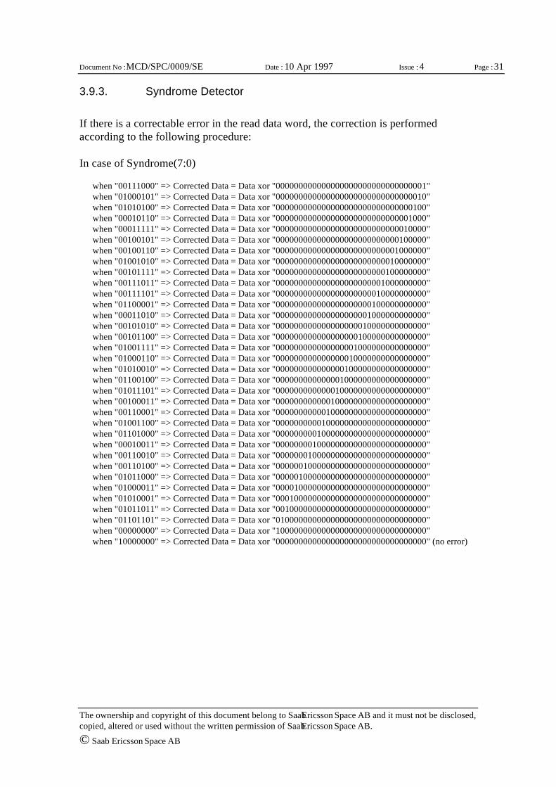
3.9.3. Syndrome Detector
If there is a correctable error in the read data word, the correction is performedaccording to the following procedure:
In case of Syndrome(7:0)
when "00111000" => Corrected Data = Data xor "000000000000000000000000000000001" when "01000101" => Corrected Data = Data xor "000000000000000000000000000000010" when "01010100" => Corrected Data = Data xor "000000000000000000000000000000100" when "00010110" => Corrected Data = Data xor "000000000000000000000000000001000" when "00011111" => Corrected Data = Data xor "000000000000000000000000000010000" when "00100101" => Corrected Data = Data xor "000000000000000000000000000100000" when "00100110" => Corrected Data = Data xor "000000000000000000000000001000000" when "01001010" => Corrected Data = Data xor "000000000000000000000000010000000" when "00101111" => Corrected Data = Data xor "000000000000000000000000100000000" when "00111011" => Corrected Data = Data xor "000000000000000000000001000000000" when "00111101" => Corrected Data = Data xor "000000000000000000000010000000000" when "01100001" => Corrected Data = Data xor "000000000000000000000100000000000" when "00011010" => Corrected Data = Data xor "000000000000000000001000000000000" when "00101010" => Corrected Data = Data xor "000000000000000000010000000000000" when "00101100" => Corrected Data = Data xor "000000000000000000100000000000000" when "01001111" => Corrected Data = Data xor "000000000000000001000000000000000" when "01000110" => Corrected Data = Data xor "000000000000000010000000000000000" when "01010010" => Corrected Data = Data xor "000000000000000100000000000000000" when "01100100" => Corrected Data = Data xor "000000000000001000000000000000000" when "01011101" => Corrected Data = Data xor "000000000000010000000000000000000" when "00100011" => Corrected Data = Data xor "000000000000100000000000000000000" when "00110001" => Corrected Data = Data xor "000000000001000000000000000000000" when "01001100" => Corrected Data = Data xor "000000000010000000000000000000000" when "01101000" => Corrected Data = Data xor "000000000100000000000000000000000" when "00010011" => Corrected Data = Data xor "000000001000000000000000000000000" when "00110010" => Corrected Data = Data xor "000000010000000000000000000000000" when "00110100" => Corrected Data = Data xor "000000100000000000000000000000000" when "01011000" => Corrected Data = Data xor "000001000000000000000000000000000" when "01000011" => Corrected Data = Data xor "000010000000000000000000000000000" when "01010001" => Corrected Data = Data xor "000100000000000000000000000000000" when "01011011" => Corrected Data = Data xor "001000000000000000000000000000000" when "01101101" => Corrected Data = Data xor "010000000000000000000000000000000" when "00000000" => Corrected Data = Data xor "100000000000000000000000000000000" when "10000000" => Corrected Data = Data xor "000000000000000000000000000000000" (no error)
Page : 32
The ownership and copyright of this document belong to Saab Ericsson Space AB and it must not be disclosed,copied, altered or used without the written permission of Saab Ericsson Space AB.
© Saab Ericsson Space AB
Document No : MCD/SPC/0009/SE Date : 10 Apr 1997 Issue : 4
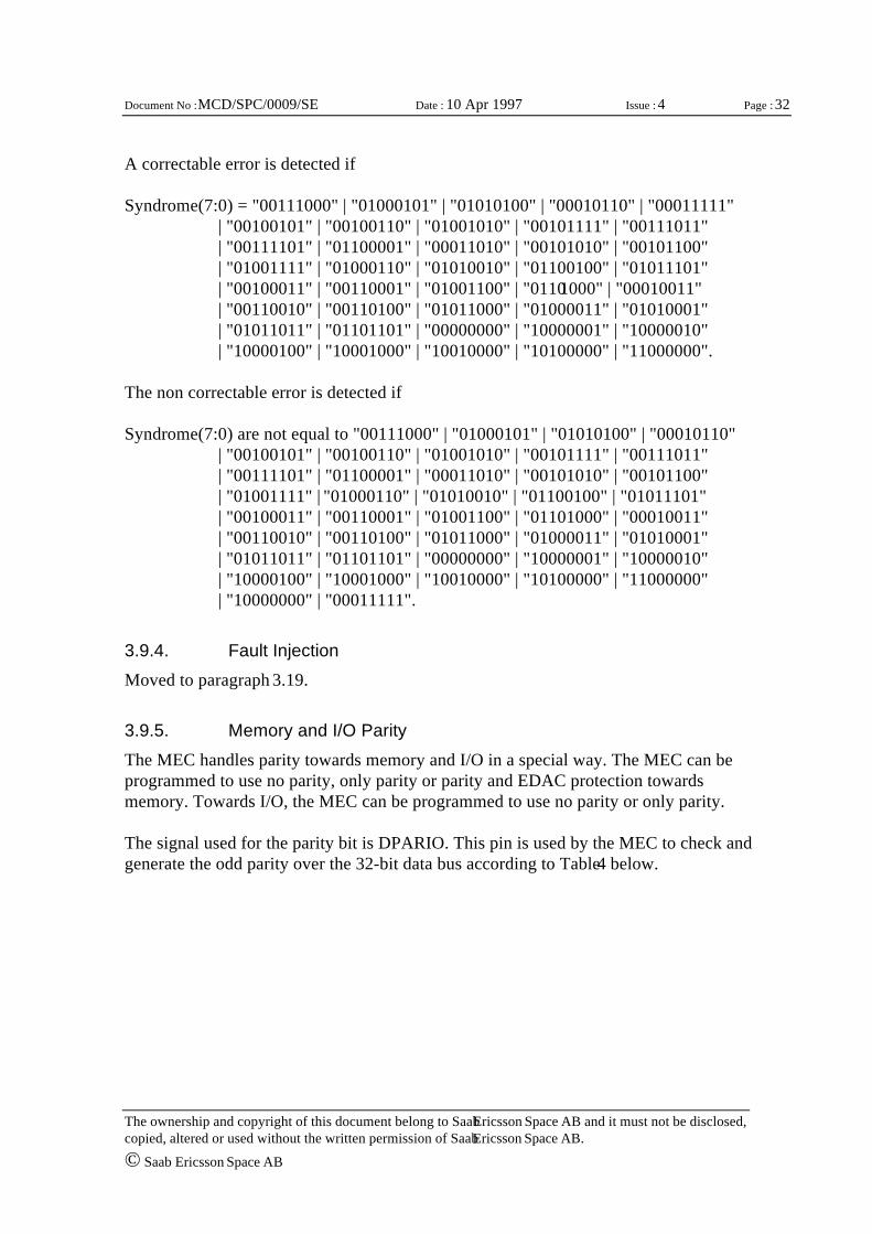
A correctable error is detected if
Syndrome(7:0) = "00111000" | "01000101" | "01010100" | "00010110" | "00011111"| "00100101" | "00100110" | "01001010" | "00101111" | "00111011"| "00111101" | "01100001" | "00011010" | "00101010" | "00101100"| "01001111" | "01000110" | "01010010" | "01100100" | "01011101"| "00100011" | "00110001" | "01001100" | "01101000" | "00010011"| "00110010" | "00110100" | "01011000" | "01000011" | "01010001"| "01011011" | "01101101" | "00000000" | "10000001" | "10000010"| "10000100" | "10001000" | "10010000" | "10100000" | "11000000".
The non correctable error is detected if
Syndrome(7:0) are not equal to "00111000" | "01000101" | "01010100" | "00010110"| "00100101" | "00100110" | "01001010" | "00101111" | "00111011"| "00111101" | "01100001" | "00011010" | "00101010" | "00101100"| "01001111" | "01000110" | "01010010" | "01100100" | "01011101"| "00100011" | "00110001" | "01001100" | "01101000" | "00010011"| "00110010" | "00110100" | "01011000" | "01000011" | "01010001"| "01011011" | "01101101" | "00000000" | "10000001" | "10000010"| "10000100" | "10001000" | "10010000" | "10100000" | "11000000"
| "10000000" | "00011111".
3.9.4. Fault Injection
Moved to paragraph 3.19.
3.9.5. Memory and I/O Parity
The MEC handles parity towards memory and I/O in a special way. The MEC can beprogrammed to use no parity, only parity or parity and EDAC protection towardsmemory. Towards I/O, the MEC can be programmed to use no parity or only parity.
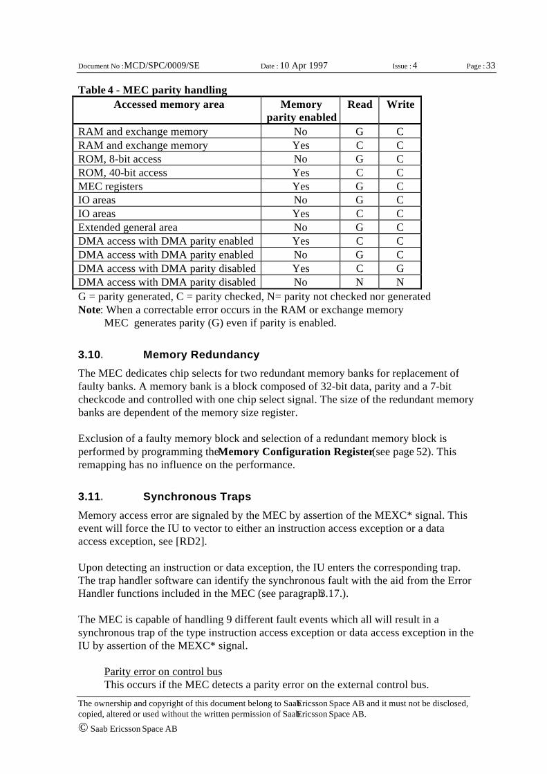
The signal used for the parity bit is DPARIO. This pin is used by the MEC to check andgenerate the odd parity over the 32-bit data bus according to Table 4 below.
Page : 33
The ownership and copyright of this document belong to Saab Ericsson Space AB and it must not be disclosed,copied, altered or used without the written permission of Saab Ericsson Space AB.
© Saab Ericsson Space AB
Document No : MCD/SPC/0009/SE Date : 10 Apr 1997 Issue : 4
3.10. Memory Redundancy
The MEC dedicates chip selects for two redundant memory banks for replacement offaulty banks. A memory bank is a block composed of 32-bit data, parity and a 7-bitcheckcode and controlled with one chip select signal. The size of the redundant memorybanks are dependent of the memory size register.
Exclusion of a faulty memory block and selection of a redundant memory block isperformed by programming the Memory Configuration Register (see page 52). Thisremapping has no influence on the performance.
3.11. Synchronous Traps
Memory access error are signaled by the MEC by assertion of the MEXC* signal. Thisevent will force the IU to vector to either an instruction access exception or a dataaccess exception, see [RD2].
Upon detecting an instruction or data exception, the IU enters the corresponding trap.The trap handler software can identify the synchronous fault with the aid from the ErrorHandler functions included in the MEC (see paragraph 3.17.).
The MEC is capable of handling 9 different fault events which all will result in asynchronous trap of the type instruction access exception or data access exception in theIU by assertion of the MEXC* signal.
Parity error on control busThis occurs if the MEC detects a parity error on the external control bus.
Table 4 - MEC parity handlingAccessed memory area Memory
parity enabledRead Write
RAM and exchange memory No G CRAM and exchange memory Yes C CROM, 8-bit access No G CROM, 40-bit access Yes C CMEC registers Yes G CIO areas No G CIO areas Yes C CExtended general area No G CDMA access with DMA parity enabled Yes C CDMA access with DMA parity enabled No G CDMA access with DMA parity disabled Yes C GDMA access with DMA parity disabled No N NG = parity generated, C = parity checked, N= parity not checked nor generatedNote: When a correctable error occurs in the RAM or exchange memory
MEC generates parity (G) even if parity is enabled.
Page : 34
The ownership and copyright of this document belong to Saab Ericsson Space AB and it must not be disclosed,copied, altered or used without the written permission of Saab Ericsson Space AB.
© Saab Ericsson Space AB
Document No : MCD/SPC/0009/SE Date : 10 Apr 1997 Issue : 4
Parity error on the data busThis trap occurs if the MEC detects a parity error on the external data bus.
Parity error on address busThis trap occurs if the MEC detects a parity error on the external address bus.
Access to protected areaThis trap occurs if any addressing device performs an access which does not matchthe memory protection scheme.
Access to unimplemented areaThis trap occurs if any addressing device performs an access with invalid addressto an unimplemented area.
MEC register access violationThis trap occurs if an illegal access is attempted to an internal MEC register.
Uncorrectable error in memoryThe trap occurs if the EDAC detects a non-correctable error.
Bus time-outThis trap occurs if the ready generation times out i.e. if, during a BUSRDY*controlled access, BUSRDY* is not asserted within 256 clock cycles.
System bus errorThis trap occurs if the Bus error (BUSERR*) input is asserted.
3.12. Interrupts (Asynchronous Traps)
The MEC handles 15 different events corresponding to asynchronous traps.
The MEC allocates each specific interrupt to an interrupt level. The interrupt allocationis in accordance with the scheme in Table 5 (page 36).
The following interrupts, representing asynchronous traps, asserts the Interrupt RequestLevel (IRL) inputs of the processor:
Watch Dog time-outThis interrupt occurs if the watchdog timer times out.
DMA time-outThis interrupt occurs if the DMA session exceeds permitted time.
DMA access errorThis interrupt occurs if the DMA performs an access violation or illegal access.
Page : 35
The ownership and copyright of this document belong to Saab Ericsson Space AB and it must not be disclosed,copied, altered or used without the written permission of Saab Ericsson Space AB.
© Saab Ericsson Space AB
Document No : MCD/SPC/0009/SE Date : 10 Apr 1997 Issue : 4
UART errorThis interrupt is generated by the UARTs if an error is detected.
UART A and B Data Ready or Transmitter ReadyThese interrupts are generated by the UARTs each time a data word has beencorrectly received and each time a data word has been sent.
Real Time ClockThis interrupt is issued by the real time clock timer tick.
General purpose timerThis interrupt is issued by the general purpose timer.
Correctable error in memoryThis interrupt occurs if the EDAC detects and corrects an error.
Masked Hardware ErrorsThis occurs when there is a hardware error set in the Error and Reset StatusRegister (see page 61) and the error is masked (an unmasked hardware error leadsto an Error Halt or Warm Reset instead of an interrupt, see paragraph 3.5.).
5 external individually prioritized interruptsThe sources of these interrupts are located outside the ERC32. Consequently theseinterrupts are inputs to the MEC.
The interrupt allocation for the asynchronous traps is in accordance with the scheme inTable 5 (page 36).
It is possible to mask each individual interrupt (except interrupt 15) by setting thecorresponding bit in the Interrupt Mask Register (see page 57).
The MEC includes a specific register called Interrupt Pending Register (see page 56),which reflects the pending interrupts. It is possible to clear pending interrupts by settingthe corresponding bit in the Interrupt Clear Register (see page 57).
(Interrupt test description moved to paragraph 3.19.)
The interrupts in the IPR are cleared automatically when the interrupt is acknowledged.The MEC will sample the trap address in order to know which bit to clear.
Upon receiving an interrupt, external or forced, the MEC issues a request on its IRLoutputs to the IU with the corresponding interrupt level. If two or more interrupts occursimultaneously, the interrupt with the highest priority level is issued to the IU. If a higherlevel interrupt is recognized by the MEC before the lower level interrupt request isacknowledged, the higher level interrupt will replace the lower level interrupt request.
Page : 36
The ownership and copyright of this document belong to Saab Ericsson Space AB and it must not be disclosed,copied, altered or used without the written permission of Saab Ericsson Space AB.
© Saab Ericsson Space AB
Document No : MCD/SPC/0009/SE Date : 10 Apr 1997 Issue : 4
By programming the Interrupt Shape Register (see page 56), it is possible to define theexternal interrupts to be either active low or active high and to define the externalinterrupts to be either edge or level sensitive. Also, by programming the ISR, it ispossible to make one of the external interrupts generate a pulse on the EXTINTACKoutput when the IU acknowledges the interrupt.
The external interrupt inputs are filtered such that both level and edge sensitive interruptsare detected only if the external interrupt is active for at least two system clock cycles.
Edge sensitive interrupts will be detected only when a transition occurs (from high tolow if programmed to be active low and vice-versa), i.e. the corresponding bit in IPR willbe set.
Level sensitive interrupts will be detected, i.e. the corresponding bit in IPR will be set aslong as the interrupt line is asserted. When the interrupt line is deasserted, thecorresponding bit in IPR will be cleared.
Table 5 - Interrupt Trap Type and default priority assignmentsTrap Priority Trap Type Interrupt level/noWatch Dog time-out 13 0x1F 15Ext. Interrupt 4 14 0x1E 14Real Time Clock 15 0x1D 13General purpose timer 16 0x1C 12Ext. Interrupt 3 17 0x1B 11Ext. Interrupt 2 18 0x1A 10DMA time-out 19 0x19 9DMA access error 20 0x18 8UART error 21 0x17 7Correctable error in mem. 22 0x16 6UART B Data Ready orTransmitter Ready
23 0x15 5
UART A Data Ready orTransmitter Ready
24 0x14 4
Ext. Interrupt 1 25 0x13 3Ext. Interrupt 0 26 0x12 2Masked Hardware errors 27 0x11 1
Page : 37
The ownership and copyright of this document belong to Saab Ericsson Space AB and it must not be disclosed,copied, altered or used without the written permission of Saab Ericsson Space AB.
© Saab Ericsson Space AB
Document No : MCD/SPC/0009/SE Date : 10 Apr 1997 Issue : 4
3.13. General Purpose and Real Time Clock Timers
Two timers (apart from the special Watchdog timer) are available in the MEC. Thesetimers provide, in addition to a generalized counter mechanisms, a mechanism for settingthe step size in which actual time counts are performed (a two-stage counter). Eachtimer/counter pulse generator consists of two parts:- pre-SCALER- COUNTER
SCALER is a counter to adjust the step size in which COUNTER does the actual timecount.
COUNTER is a counter to actually count time in steps as set by the value in SCALER.COUNTER is decrements when SCALER reaches zero.
The implementation is shown in Figure 6.
Timer function
Figure 6 - Timer implementation
Both timers are clocked by the internal system clock. The timers are programmable bywriting to the Timer Control Register (see page 59). They are possible to program tobe either of single-shot type or periodical type, in both cases generate an interrupt whenthe delay time has elapsed. If the timer is not programmed with a new value when set toperiodical type, it restarts from the latest programmed value and continue to count down,thus generating interrupts periodically. The Real Time Clock Timer interrupt hashigher priority than the General Purpose Timer interrupt. It is possible to halt andrestart the timers by writing to the Timer Control Register. The only functionaldifference between the two timers is that the Real Time Clock Timer has an 8-bit scalerwhile the General Purpose Timer has a 16-bit scaler providing a wider range.
While the signal CPUHALT* is active, the timers are temporary halted.
Page : 38
The ownership and copyright of this document belong to Saab Ericsson Space AB and it must not be disclosed,copied, altered or used without the written permission of Saab Ericsson Space AB.
© Saab Ericsson Space AB
Document No : MCD/SPC/0009/SE Date : 10 Apr 1997 Issue : 4
The Real Time Clock Timer (see page 58) is implemented as one down counting 8-bitscaler and one down counting 32-bit counter. The current value of the scaler and counterof the Real Time Clock can be read.
The timer scaler load value is programmable in Real Time Clock Program Register<Scaler> (see page 58). The timer count load value is programmable in Real TimeClock Program Register <Counter> (see page 58). The value of these registers willnot be altered unless reprogrammed or reset. After system reset the Real Time Clock isnot running and must be programmed as required.
The General Purpose Timer (see page 58) is implemented as one down counting 16-bitscaler and one down counting 32-bit counter. The current value of the scaler and counterof the General Purpose Timer can be read.
The timer scaler load value is programmable in General Purpose Timer ProgramRegister <Scaler> (see page 58). The timer count load value is programmable inGeneral Purpose Timer Program Register <Counter> (see page 58). The value ofthese registers will not be altered unless reprogrammed or reset. After system reset theGeneral Purpose Timer is not running and must be programmed as required.
Page : 39
The ownership and copyright of this document belong to Saab Ericsson Space AB and it must not be disclosed,copied, altered or used without the written permission of Saab Ericsson Space AB.
© Saab Ericsson Space AB
Document No : MCD/SPC/0009/SE Date : 10 Apr 1997 Issue : 4
3.14. Watch Dog
The watch dog function consists of a Watchdog Timer (see page 57). The watch dog issupplied from a separate external input (WDCLK) which must have a frequency which isat least three times lower than SYSCLK. This input could be divided by 16 in a prescaleror routed directly to the scaler of the watch dog as set in the MEC Control Register(see page 51).
The WDCLK input consists of a Schmitt-trigger to allow clock supply from an externalRC oscillator.
It is possible to program the timer by setting a specific value in the Watchdog Programand Timeout Acknowledge Register (see page 57). The register consists of one scalerfield and one counter field corresponding directly to the scaler field and the counter fieldof the watchdog timer.
After system reset or processor reset, the timer is enabled and starts running. The defaultvalue is the scaler set to maximum and the counter set to maximum. By writing to theTrap Door Set (see page 57) after system reset, the timer can be disabled. After thedisabling of the watch dog timer a write operation to the Watchdog Program andTimeout Acknowledge Register (see page 57) starts the timer counting with the valueof the specified fields. Note that the Watchdog cannot be disabled once the WatchdogProgram and Timeout Acknowledge Register has been written.
If the timer is refreshed by writing to Watchdog Program and Timeout AcknowledgeRegister (see page 57) before the counter reaches zero value, the timer restarts thecounting with the new delay value. If the timer is not refreshed (reprogrammed) beforethe counter reaches zero value, an interrupt is issued to the IU. Simultaneously, the timerstarts counting a reset timeout period with the programmed delay time. Then, if the timeris acknowledged by writing to Watchdog Program and Timeout AcknowledgeRegister (see page 57) with a new programmed value before the reset timeout periodelapses again, the timer restarts counting with the new delay value, but if the timer is notacknowledged before the reset timeout period elapses, a processor reset is issued by theMEC.
The Watchdog is temporary halted when the CPUHALT* signal is active.
Figure 7 explains all the states and transitions of the watchdog timer.
Page : 40
The ownership and copyright of this document belong to Saab Ericsson Space AB and it must not be disclosed,copied, altered or used without the written permission of Saab Ericsson Space AB.
© Saab Ericsson Space AB
Document No : MCD/SPC/0009/SE Date : 10 Apr 1997 Issue : 4
WDInit
default value
Trap Door set
WD disabled
WatchdogProgram(new value)
WD enabled
normal mode
Reset Timeout
Processor reset
WDReset timer enabled
WD halted
System / processor reset
Interrupt
Watchdog Program (New value)
Watchdog Timeout Watchdog Timeout acknowledge
(New value)
Watchdog timeout
Watchdog Program
(Refresh)
Figure 7 - Watchdog timer states and transitions
Page : 41
The ownership and copyright of this document belong to Saab Ericsson Space AB and it must not be disclosed,copied, altered or used without the written permission of Saab Ericsson Space AB.
© Saab Ericsson Space AB
Document No : MCD/SPC/0009/SE Date : 10 Apr 1997 Issue : 4
3.15. UART
The MEC includes two full duplex asynchronous receiver transmitters (UARTs).
The data format of the UARTs is eight bits. It is possible to choose between even or oddparity, or no parity, and between one and two stop bits by programming the MECControl Register (see page 51). After system reset odd parity and one stop bit are set.The baud rate of the UART is set by programming the MEC Control Register (seepage 51). After system reset the baud rate is set to system clock frequency divided by 32which is probably not a usable baud rate. It follows that the baud rate in the MECControl Register must be programmed after system reset.
The UARTs provides double buffering, i.e. each UART consists of a transmitter holdingregister, a receiver holding register, a transmitter shift register, and a receiver shiftregister. Each of these registers has a width of 8 bits. For each UART a RX and TXRegister (see page 62) is provided. There is also a common UART Status Register (seepage 62).
Figure 9 - removedThe receiver converts serial start bit, data word, parity bit and stop bit(s) into parallelform. The transmitter converts parallel data into serial form automatically adding startbit, parity bit, and stop bit(s).
To output a byte on the serial output the following procedure should be followed. First,the UART Status Register should be read in order to check that the transmitter holdingregister (THE, bit 2 and bit 18 respectively for channel A and B) is empty. Otherwise,the previous byte to be output may be lost (note that the TSE bit is not useful for thepurpose of checking if a character may be written to the RX/TX register). Then, the byteto be output (RTD, bits 0-7) is written in the RX and TX register. The byte written willthen automatically be transferred to the transmitter send register and converted to serialform also adding start bit, parity bit, and stop bit(s). The above described sequence canbe part of a trap handler for the UART interrupt.
When a data byte has been received on the serial interface an interrupt is issued to theIU. The byte received is converted to parallel form and loaded into the receiver dataregister. Framing error, i.e. the stop bit is not of correct polarity, parity error, andoverrun error, i.e. the preceding byte has not been read before a complete following byteis received, are indicated by the bits FE, PE, and OE, respectively in the UART statusregister.A correctly received byte is indicated by the Data Ready bits for channel A and B (DRA,bit 0 and DRB, bit 16) when reading the UART status register.
The UARTs generate an interrupt each time a data word has been received, a data wordhas been sent, and if an error is detected. There is one interrupt from each UART (A andB) to indicate that data is correctly received or that the transmitter register is empty.There is another interrupt to indicate errors, but this interrupt is common for both UARTchannels.
Page : 42
The ownership and copyright of this document belong to Saab Ericsson Space AB and it must not be disclosed,copied, altered or used without the written permission of Saab Ericsson Space AB.
© Saab Ericsson Space AB
Document No : MCD/SPC/0009/SE Date : 10 Apr 1997 Issue : 4
The UART uses an internal clock which is 16 times faster than the baud-rate, andsamples each bit 16 times, to ensure error free reception. The clock is derived either fromthe system clock or can use the watchdog clock with a UART oscillator input.
The baudrate of the UARTs can be programmed in the Scaler field and UBR bit of theMEC Control Register. The scaler shall be set to:
ClockScaler = - 1
32 * Baudrate * (2 - UBR)
Where Clock is either the frequency of the system clock (SYSCLK) or the watchdogclock (WDCLK) selected by UCS (bit 23 in MEC Control Register). UBR is the valueof the UBR bit. Baudrate is the desired baudrate. Note that the resulting actual baudratewill probably not be exactly the desired one. This is due to the fact that Scaler is aninteger number, and the above given equation may yield a non-integer result, dependingon the Clock frequency.
The UART is temporary halted when CPUHALT* is active and no transmission isperformed by the UART.
The external UART interfaces consist of one transmit data output for each UARTchannel (TXA and TXB) and one receive data input for each UART channel (RXA andRXB).
Note that no hardware handshake signals, such as CTS or RTS are implemented. Anyhandshaking must be implemented in software (e.g. using XON/XOFF).
3.16. Parity Checking
The MEC includes parity checking and generation if required on the external data bus(DPARIO). It includes parity checking on the external address bus (APAR). It alsoincludes parity checking on ASI and SIZE (ASPAR) together with parity generation andchecking on all internal registers. The MEC also includes parity generation and checkingon the external control bus to the IU (IMPAR). If a parity error is detected on theexternal data bus, the external address, the external ASI and SIZE, the external controlbus, the memory exception output (MEXC*) is asserted. If a memory exception eventoccurs the System Fault Status Register (see page 60) is updated and reflects the typeand location of parity errors.All external parity checking can be disabled using the NOPAR* signal.
3.17. Error Handler
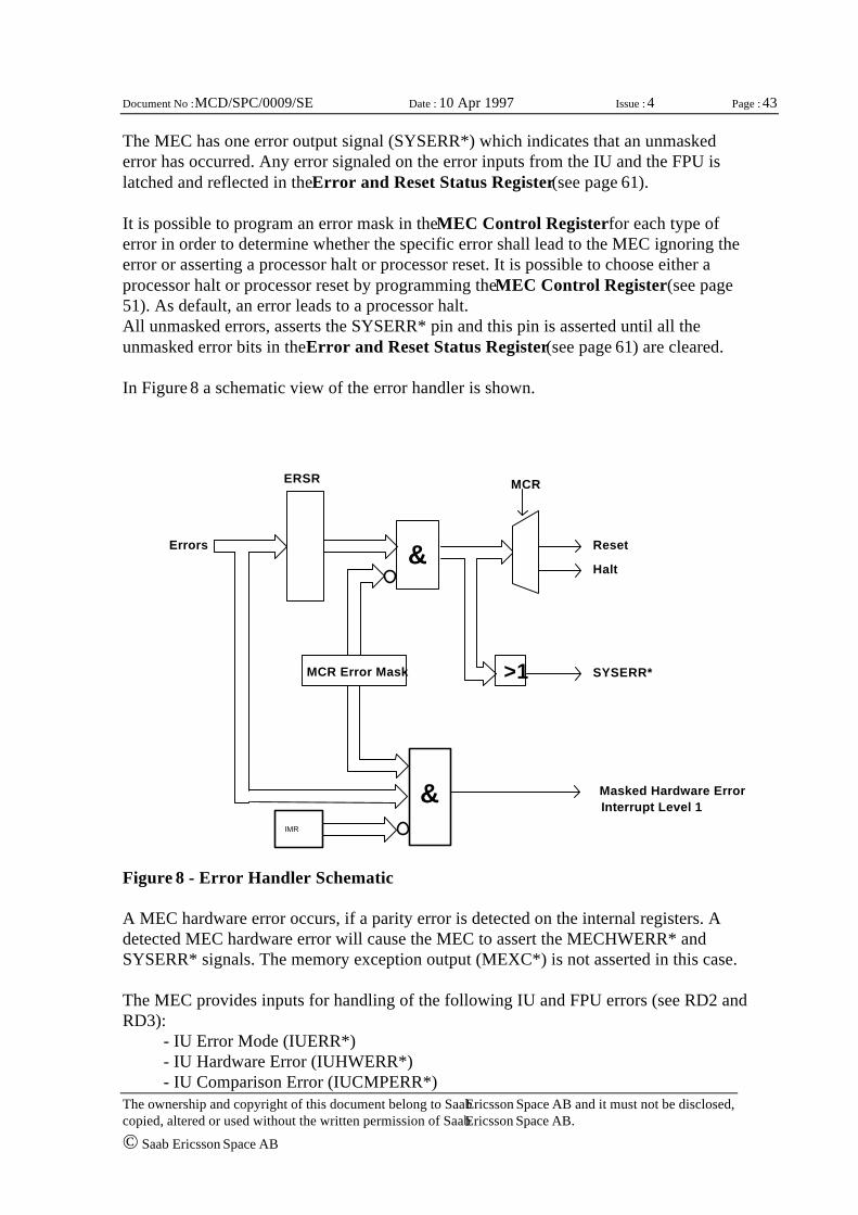
Page : 43
The ownership and copyright of this document belong to Saab Ericsson Space AB and it must not be disclosed,copied, altered or used without the written permission of Saab Ericsson Space AB.
© Saab Ericsson Space AB
Document No : MCD/SPC/0009/SE Date : 10 Apr 1997 Issue : 4
The MEC has one error output signal (SYSERR*) which indicates that an unmaskederror has occurred. Any error signaled on the error inputs from the IU and the FPU islatched and reflected in the Error and Reset Status Register (see page 61).
It is possible to program an error mask in the MEC Control Register for each type oferror in order to determine whether the specific error shall lead to the MEC ignoring theerror or asserting a processor halt or processor reset. It is possible to choose either aprocessor halt or processor reset by programming the MEC Control Register (see page51). As default, an error leads to a processor halt.All unmasked errors, asserts the SYSERR* pin and this pin is asserted until all theunmasked error bits in the Error and Reset Status Register (see page 61) are cleared.
In Figure 8 a schematic view of the error handler is shown.
A MEC hardware error occurs, if a parity error is detected on the internal registers. Adetected MEC hardware error will cause the MEC to assert the MECHWERR* andSYSERR* signals. The memory exception output (MEXC*) is not asserted in this case.
The MEC provides inputs for handling of the following IU and FPU errors (see RD2 andRD3):
- IU Error Mode (IUERR*)- IU Hardware Error (IUHWERR*)- IU Comparison Error (IUCMPERR*)
ERSR MCR
MCR Error Mask
Errors Reset
Halt&
>1 SYSERR*
IMR
& Masked Hardware Error Interrupt Level 1
Figure 8 - Error Handler Schematic
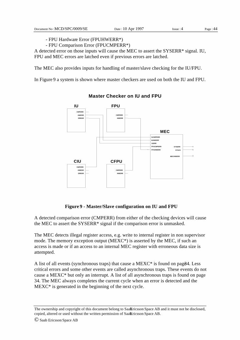
Page : 44
The ownership and copyright of this document belong to Saab Ericsson Space AB and it must not be disclosed,copied, altered or used without the written permission of Saab Ericsson Space AB.
© Saab Ericsson Space AB
Document No : MCD/SPC/0009/SE Date : 10 Apr 1997 Issue : 4
- FPU Hardware Error (FPUHWERR*)- FPU Comparison Error (FPUCMPERR*)
A detected error on those inputs will cause the MEC to assert the SYSERR* signal. IU,FPU and MEC errors are latched even if previous errors are latched.
The MEC also provides inputs for handling of master/slave checking for the IU/FPU.
In Figure 9 a system is shown where master checkers are used on both the IU and FPU.
A detected comparison error (CMPERR) from either of the checking devices will causethe MEC to assert the SYSERR* signal if the comparison error is unmasked.
The MEC detects illegal register access, e.g. write to internal register in non supervisormode. The memory exception output (MEXC*) is asserted by the MEC, if such anaccess is made or if an access to an internal MEC register with erroneous data size isattempted.
A list of all events (synchronous traps) that cause a MEXC* is found on page 34. Lesscritical errors and some other events are called asynchronous traps. These events do notcause a MEXC* but only an interrupt. A list of all asynchronous traps is found on page34. The MEC always completes the current cycle when an error is detected and theMEXC* is generated in the beginning of the next cycle.
IU FPU
MEC
CMPERR
HWERR
ERROR
CMPERR
HWERR
IUCMPERR
IUHWERR
IUERR
FPUCMPERR
FPUHWERR
SYSERR
SYSAV
CIU CFPUCMPERR
HWERR
ERROR
CMPERR
HWERR
MECHWERR
Master Checker on IU and FPU
Figure 9 - Master/Slave configuration on IU and FPU
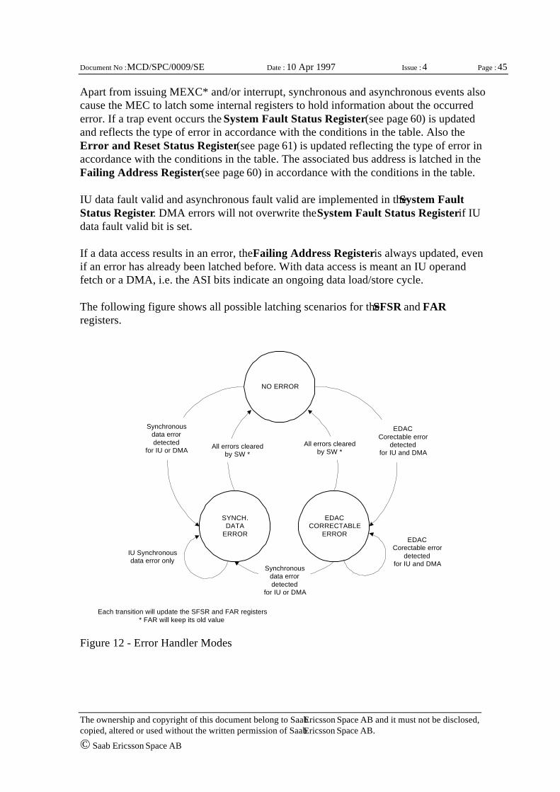
Page : 45
The ownership and copyright of this document belong to Saab Ericsson Space AB and it must not be disclosed,copied, altered or used without the written permission of Saab Ericsson Space AB.
© Saab Ericsson Space AB
Document No : MCD/SPC/0009/SE Date : 10 Apr 1997 Issue : 4
Apart from issuing MEXC* and/or interrupt, synchronous and asynchronous events alsocause the MEC to latch some internal registers to hold information about the occurrederror. If a trap event occurs the System Fault Status Register (see page 60) is updatedand reflects the type of error in accordance with the conditions in the table. Also theError and Reset Status Register (see page 61) is updated reflecting the type of error inaccordance with the conditions in the table. The associated bus address is latched in theFailing Address Register (see page 60) in accordance with the conditions in the table.
IU data fault valid and asynchronous fault valid are implemented in the System FaultStatus Register. DMA errors will not overwrite the System Fault Status Register if IUdata fault valid bit is set.
If a data access results in an error, the Failing Address Register is always updated, evenif an error has already been latched before. With data access is meant an IU operandfetch or a DMA, i.e. the ASI bits indicate an ongoing data load/store cycle.
The following figure shows all possible latching scenarios for the SFSR and FARregisters.
Figure 12 - Error Handler Modes
NO ERROR
SYNCH.DATA
ERROR
EDACCORRECTABLE
ERROR
EDACCorectable error
detectedfor IU and DMA
Synchronousdata errordetected
for IU or DMAAll errors cleared
by SW *All errors cleared
by SW *
EDACCorectable error
detectedfor IU and DMA
IU Synchronousdata error only
Synchronousdata errordetected
for IU or DMA
Each transition will update the SFSR and FAR registers* FAR will keep its old value
Page : 46
The ownership and copyright of this document belong to Saab Ericsson Space AB and it must not be disclosed,copied, altered or used without the written permission of Saab Ericsson Space AB.
© Saab Ericsson Space AB
Document No : MCD/SPC/0009/SE Date : 10 Apr 1997 Issue : 4
The following tables show when updating of the registers is made.
Synchronous trap events SFSR FARControl bus parity error U UAddress bus parity error U UData bus parity error U UMemory access protectionerror
U U
Unimplemented addressviolation
U U
MEC register violation error U UEDAC uncorrectable error U UBus time-out U USystem bus error U U
Asynchronous trap events SFSR ERSR FARWatchdog timeout * U UExt. interrupt 4Real time clock interruptGeneral purpose timer interruptExt. interrupt 3Ext. interrupt 2DMA session timeout UDMA access error U UUART error interrupt UEDAC correctable error U UUART B data received or transmitterready interruptUART A data received ortransmitter ready interruptExt. interrupt 1Ext. interrupt 0Masked hardware error interrupt U
U : register updated, parity updatedSFSR : System Fault Status registerERSR : Error and Reset Status RegisterFAR : Failing Address Register* SFSR is updated at the time of Watchdog interrupt while ERSR is only updated if theWatchdog elapsed causes a halt or reset.
Page : 47
The ownership and copyright of this document belong to Saab Ericsson Space AB and it must not be disclosed,copied, altered or used without the written permission of Saab Ericsson Space AB.
© Saab Ericsson Space AB
Document No : MCD/SPC/0009/SE Date : 10 Apr 1997 Issue : 4
3.18. System Availability
The SYSAV bit in the Error and Reset Status Register (see page 61) can be used bysoftware to indicate system availability. The SYSAV bit is cleared by reset and isprogrammable by software. Note that the SYSAV output of the MEC will be assertedonly if the SYSAV bit is set and SYSERR* is deasserted, i.e. no error has been detected.
3.19. Test mode and Test Access Port
The MEC includes a number of test facilities such as EDAC test, Parity test, Interrupttest, Error test and a simple Test Access Port. These test functions are controlled usingthe Test Control Register (TCR) (see page 61).
3.19.1. EDAC Test
The EDAC function allows fault injection for memory test purposes and also test of theEDAC function itself. By enabling EDAC test mode in TCR (ET=1), the bits in the CBfield of TCR will substitute the normal checkbits during store cycles.
3.19.2. Parity Test
The MEC register parity function allows fault injection for parity test purposes. Byenabling parity test mode in TCR (PT=1), wrong parity will be generated when any MECregister is read.
3.19.3. Interrupt Test
It is possible to test and force interrupts by setting the corresponding bit in the InterruptForce Register (page 57). Clearing of interrupts by setting the corresponding bit in theInterrupt Clear Register (ICR) will always clear the corresponding bit(s) in theInterrupt Pending Register (IPR), but will never affect the interrupts set in theInterrupt Force Register (IFR). However, it is possible to remove these interrupts byclearing the corresponding bit in IFR.
If the MEC is in interrupt test mode the handling of IFR and IPR is different:
When "Interrupt test" is not enabled:- Setting or clearing a bit in IFR will only affect IFR. The corresponding
interrupt will not be forced.- When the interrupt is acknowledged, the MEC will automatically clear the
bit in the IPR corresponding to the trap address as described above.
When "Interrupt test" is enabled:- Setting a bit in IFR will force the corresponding interrupt if it is not masked
in IMR.
Page : 48
The ownership and copyright of this document belong to Saab Ericsson Space AB and it must not be disclosed,copied, altered or used without the written permission of Saab Ericsson Space AB.
© Saab Ericsson Space AB
Document No : MCD/SPC/0009/SE Date : 10 Apr 1997 Issue : 4
- When the interrupt is acknowledged, the MEC will automatically clear thecorresponding bit in the IFR if this bit is set, otherwise it will clear thecorresponding bit in the IPR. In this way no external interrupts are lost.
Interrupt test mode is enabled in the Test Control Register (see page 61).
3.19.4. Error Test
The MEC error detection and handling allows fault injection for test purpose. Byenabling Error test mode in TCR (EWE=1), an error could be simulated by writing to theError and Reset Status Register, bits 5-0.
3.19.5. Test Access Port (TAP)
The MEC includes a Test Access Port (TAP) interface (IEEE standard 1149.1) fordebugging and test purposes. The TAP does however not implement any scan function inthe present version of the MEC, and only implements the Bypass register.
The timing of the TAP signals is according to IEEE 1149.1. This means that TDI andTMS are sampled by the ERC32 devices on the rising edge of TCK, and that TDO isdriven on the falling edge .
Figure 12 - removed
3.20. System Clock
The MEC provides a system clock signal (SYSCLK) with a nominal 50 % duty cycle forthe IU/FPU and the rest of the system.
The system clock is obtained by dividing an external clock signal (CLK2) by two. Pleasenote that the MEC itself uses both SYSCLK and CLK2 directly. Some MEC outputsignals are clocked by the CLK2 negative edge which means that the CLK2 duty cyclehas a direct impact on the system performance.
When interfacing peripherals (I/O interface, DMA interface etc.) it is highlyrecommended that only SYSCLK rising edge is used as reference as far as possible.CLK2 should be used as input to the MEC only.
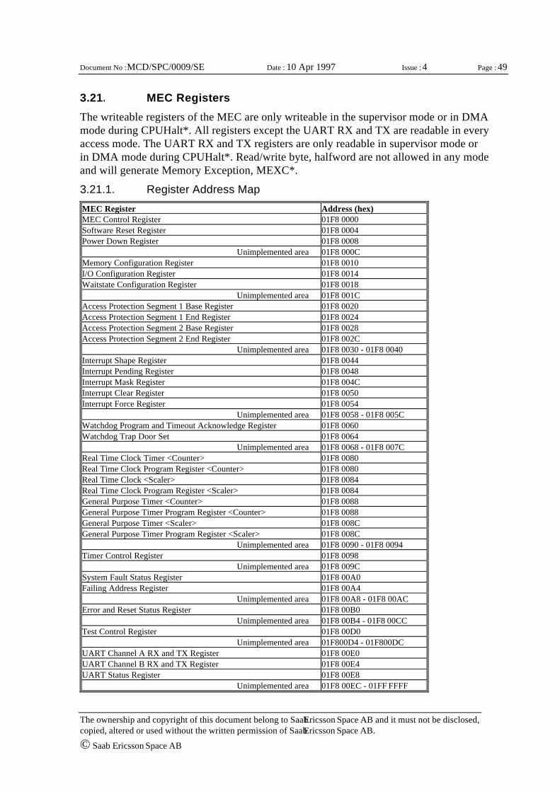
Page : 49
The ownership and copyright of this document belong to Saab Ericsson Space AB and it must not be disclosed,copied, altered or used without the written permission of Saab Ericsson Space AB.
© Saab Ericsson Space AB
Document No : MCD/SPC/0009/SE Date : 10 Apr 1997 Issue : 4
3.21. MEC Registers
The writeable registers of the MEC are only writeable in the supervisor mode or in DMAmode during CPUHalt*. All registers except the UART RX and TX are readable in everyaccess mode. The UART RX and TX registers are only readable in supervisor mode orin DMA mode during CPUHalt*. Read/write byte, halfword are not allowed in any modeand will generate Memory Exception, MEXC*.
3.21.1. Register Address Map
MEC Register Address (hex)MEC Control Register 01F8 0000Software Reset Register 01F8 0004Power Down Register 01F8 0008
Unimplemented area 01F8 000CMemory Configuration Register 01F8 0010I/O Configuration Register 01F8 0014Waitstate Configuration Register 01F8 0018
Unimplemented area 01F8 001CAccess Protection Segment 1 Base Register 01F8 0020Access Protection Segment 1 End Register 01F8 0024Access Protection Segment 2 Base Register 01F8 0028Access Protection Segment 2 End Register 01F8 002C
Unimplemented area 01F8 0030 - 01F8 0040Interrupt Shape Register 01F8 0044Interrupt Pending Register 01F8 0048Interrupt Mask Register 01F8 004CInterrupt Clear Register 01F8 0050Interrupt Force Register 01F8 0054
Unimplemented area 01F8 0058 - 01F8 005CWatchdog Program and Timeout Acknowledge Register 01F8 0060Watchdog Trap Door Set 01F8 0064
Unimplemented area 01F8 0068 - 01F8 007CReal Time Clock Timer <Counter> 01F8 0080Real Time Clock Program Register <Counter> 01F8 0080Real Time Clock <Scaler> 01F8 0084Real Time Clock Program Register <Scaler> 01F8 0084General Purpose Timer <Counter> 01F8 0088General Purpose Timer Program Register <Counter> 01F8 0088General Purpose Timer <Scaler> 01F8 008CGeneral Purpose Timer Program Register <Scaler> 01F8 008C
Unimplemented area 01F8 0090 - 01F8 0094Timer Control Register 01F8 0098
Unimplemented area 01F8 009CSystem Fault Status Register 01F8 00A0Failing Address Register 01F8 00A4
Unimplemented area 01F8 00A8 - 01F8 00ACError and Reset Status Register 01F8 00B0
Unimplemented area 01F8 00B4 - 01F8 00CCTest Control Register 01F8 00D0
Unimplemented area 01F800D4 - 01F800DCUART Channel A RX and TX Register 01F8 00E0UART Channel B RX and TX Register 01F8 00E4UART Status Register 01F8 00E8
Unimplemented area 01F8 00EC - 01FF FFFF
Page : 50
The ownership and copyright of this document belong to Saab Ericsson Space AB and it must not be disclosed,copied, altered or used without the written permission of Saab Ericsson Space AB.
© Saab Ericsson Space AB
Document No : MCD/SPC/0009/SE Date : 10 Apr 1997 Issue : 4
3.21.2. Register Configuration and Bit Allocation
For each register the following information is given:
- Address of the register
- Bits is the bit allocation of the register. A bit can either have a unique function or anumber of bits can be grouped together into a specific field.
- Name is the abbreviation for each bit or field.
- Reset value states the value for each bit or field to be obtained after the assertionof system reset.
- Function explains the function and use of each bit or field.
- r/w explains if the bit or field can be read and/or written.
Note that in some cases only part of the 32-bit register is used. The non usable bits aremarked as reserved and will always have a fix value (generally zero) when being readand can thus not be altered by a write operation.
NOTE !! All reserved bits have to be written with zeros in order to avoid parity errorresulting in a MEC internal error.
Certain registers below are not true registers in the sense that they only correspond to awrite operation with any data. Any data may be used when writing to these registers.Nevertheless, they are part of the register memory map and therefore included.
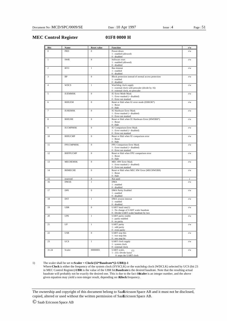
Page : 51
The ownership and copyright of this document belong to Saab Ericsson Space AB and it must not be disclosed,copied, altered or used without the written permission of Saab Ericsson Space AB.
© Saab Ericsson Space AB
Document No : MCD/SPC/0009/SE Date : 10 Apr 1997 Issue : 4
MEC Control Register 01F8 0000 H
Bits Name Reset value Function r/w0 PRD 0 Power-down
1 : enabled (allowed)0 : disabled
r/w
1 SWR 0 Software reset1 : enabled (allowed)0 : disabled
r/w
2 BTO 1 Bus timeout1 : enabled0 : disabled
r/w
3 BP 0 Block protection instead of normal access protection1 : enabled0 : disabled
r/w
4 WDCS 1 Watchdog clock supply1 : external clock with prescaler (divide by 16)0 : external clock, no prescaler
r/w
5 IUEMMSK 0 IU Error Mode Mask1 : Error masked (= disabled)0 : Error not masked
r/w
6 RHIUEM 0 Reset or Halt when IU error mode (ERROR*)1 : Reset0 : Halt
r/w
7 IUHEMSK 0 IU Hardware Error Mask1 : Error masked (= disabled)0 : Error not masked
r/w
8 RHIUHE 0 Reset or Halt when IU Hardware Error (HWERR*)1 : Reset0 : Halt
r/w
9 IUCMPMSK 0 IU Comparison Error Mask1 : Error masked (= disabled)0 : Error not masked
r/w
10 RHIUCMP 0 Reset or Halt when IU comparison error1 : Reset0 : Halt
r/w
11 FPUCMPMSK 0 FPU Comparison Error Mask1 : Error masked (= disabled)0 : Error not masked
r/w
12 RHFPUCMP 0 Reset or Halt when FPU comparison error1 : Reset0 : Halt
r/w
13 MECHEMSK 0 MEC HW Error Mask1 : Error masked (= disabled)0 : Error not masked
r/w
14 RHMECHE 0 Reset or Halt when MEC HW Error (MECHWERR)1 : Reset0 : Halt
r/w
15 reserved 0 Not used r16 DMAE 1 DMA
1 : enabled0 : disabled
r/w
17 DPE 0 DMA Parity Enabled1 : enabled0 : disabled
r/w
18 DST 1 DMA session timeout1 : enabled0 : disabled
r/w
19 UBR 0 UART baud rate(1)1 : No change of UART scaler baudrate0 : Divide UART scaler baudrate by two
r/w
20 UPE 1 UART parity enable1 : parity enabled0 : no parity
r/w
21 UP 1 UART parity1 : odd parity0 : even parity
r/w
22 USB 0 UART stop bits1 : two stop bits0 : one stop bit
r/w
23 UCS 1 UART clock supply1 : system clock0 : external clock
r/w
31-24 Scaler 00000001 UART scaler,1 - 255: Divide factor
(1)
0: stops the UART clock
r/w
1) The scaler shall be set to: Scaler = Clock/(32*Baudrate*(2-UBR))-1Where Clock is either the frequency of the system clock (SYSCLK) or the watchdog clock (WDCLK) selected by UCS (bit 23in MEC Control Register). UBR is the value of the UBR bit. Baudrate is the desired baudrate. Note that the resulting actualbaudrate will probably not be exactly the desired one. This is due to the fact that Scaler is an integer number, and the abovegiven equation may yield a non-integer result, depending on the Clock frequency.
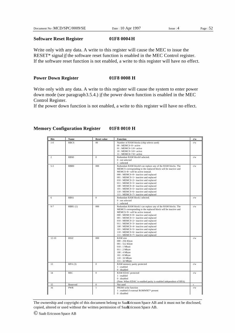
Page : 52
The ownership and copyright of this document belong to Saab Ericsson Space AB and it must not be disclosed,copied, altered or used without the written permission of Saab Ericsson Space AB.
© Saab Ericsson Space AB
Document No : MCD/SPC/0009/SE Date : 10 Apr 1997 Issue : 4
Software Reset Register 01F8 0004 H
Write only with any data. A write to this register will cause the MEC to issue theRESET* signal if the software reset function is enabled in the MEC Control register.If the software reset function is not enabled, a write to this register will have no effect.
Power Down Register 01F8 0008 H
Write only with any data. A write to this register will cause the system to enter powerdown mode (see paragraph 3.5.4.) if the power down function is enabled in the MECControl Register.If the power down function is not enabled, a write to this register will have no effect.
Memory Configuration Register 01F8 0010 H
Bits Name Reset value Function r/w1-0 RBCS 00 Number of RAM blocks (chip selects used)
00 : MEMCS<0> active01 : MEMCS<1:0> active10 : MEMCS<3:0> active11 : MEMCS<7:0> active
r/w
2 RBS0 0 Redundant RAM block0 selected.0 : not selected1 : selected
r/w
5-3 RBR0 000 Redundant RAM block0 can replace any of the RAM blocks. TheMEMCS corresponding to the replaced block will be inactive andMEMCS<8> will be active instead.000 : MEMCS<0> inactive and replaced001 : MEMCS<1> inactive and replaced010 : MEMCS<2> inactive and replaced011 : MEMCS<3> inactive and replaced100 : MEMCS<4> inactive and replaced101 : MEMCS<5> inactive and replaced110 : MEMCS<6> inactive and replaced111 : MEMCS<7> inactive and replaced
r/w
6 RBS1 0 Redundant RAM block1 selected.0 : not selected1 : selected
r/w
9-7 RBR1 (1) 000 Redundant RAM block1 can replace any of the RAM blocks. TheMEMCS corresponding to the replaced block will be inactive andMEMCS<9> will be active instead.000 : MEMCS<0> inactive and replaced001 : MEMCS<1> inactive and replaced010 : MEMCS<2> inactive and replaced011 : MEMCS<3> inactive and replaced100 : MEMCS<4> inactive and replaced101 : MEMCS<5> inactive and replaced110 : MEMCS<6> inactive and replaced111 : MEMCS<7> inactive and replaced
r/w
12-10 RSIZ 000 RAM size000 : 256 Kbyte001 : 512 Kbyte010 : 1 Mbyte011 : 2 Mbyte100 : 4 Mbyte101 : 8 Mbyte110 : 16 Mbyte111 : 32 Mbyte
r/w
13 RPA (3) 0 RAM memory parity protected1 : enabled0 : disabled
r/w
14 REC 0 RAM EDAC protected1 : enabled0 : disabled(Note: When EDAC is enabled parity is enabled independent of RPA)
r/w
15 Reserved 0 Not used r16 PWR 1 PROM write function
1 : enabled if external ROMWRT* present0 : disabled
r/w
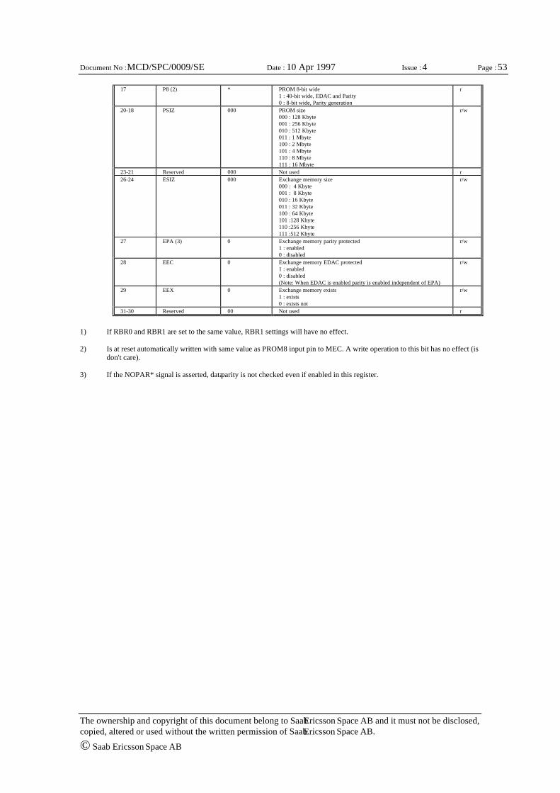
Page : 53
The ownership and copyright of this document belong to Saab Ericsson Space AB and it must not be disclosed,copied, altered or used without the written permission of Saab Ericsson Space AB.
© Saab Ericsson Space AB
Document No : MCD/SPC/0009/SE Date : 10 Apr 1997 Issue : 4
17 P8 (2) * PROM 8-bit wide1 : 40-bit wide, EDAC and Parity0 : 8-bit wide, Parity generation
r
20-18 PSIZ 000 PROM size000 : 128 Kbyte001 : 256 Kbyte010 : 512 Kbyte011 : 1 Mbyte100 : 2 Mbyte101 : 4 Mbyte110 : 8 Mbyte111 : 16 Mbyte
r/w
23-21 Reserved 000 Not used r26-24 ESIZ 000 Exchange memory size
000 : 4 Kbyte001 : 8 Kbyte010 : 16 Kbyte011 : 32 Kbyte100 : 64 Kbyte101 :128 Kbyte110 :256 Kbyte111 :512 Kbyte
r/w
27 EPA (3) 0 Exchange memory parity protected1 : enabled0 : disabled
r/w
28 EEC 0 Exchange memory EDAC protected1 : enabled0 : disabled(Note: When EDAC is enabled parity is enabled independent of EPA)
r/w
29 EEX 0 Exchange memory exists1 : exists0 : exists not
r/w
31-30 Reserved 00 Not used r
1) If RBR0 and RBR1 are set to the same value, RBR1 settings will have no effect.
2) Is at reset automatically written with same value as PROM8 input pin to MEC. A write operation to this bit has no effect (isdon't care).
3) If the NOPAR* signal is asserted, data parity is not checked even if enabled in this register.
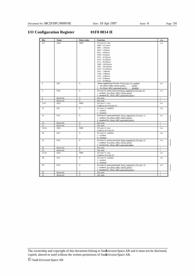
Page : 54
The ownership and copyright of this document belong to Saab Ericsson Space AB and it must not be disclosed,copied, altered or used without the written permission of Saab Ericsson Space AB.
© Saab Ericsson Space AB
Document No : MCD/SPC/0009/SE Date : 10 Apr 1997 Issue : 4
I/O Configuration Register 01F8 0014 H
Bits Name Reset value Function r/w3-0 SIZ0 0000 I/O unit<0> size.
0000 : 512 bytes0001 : 1 Kbytes0010 : 2 Kbytes0011 : 4 Kbytes0100 : 8 Kbytes0101 : 16 Kbytes0110 : 32 Kbytes0111 : 64 Kbytes1000 : 128 Kbytes1001 : 256 Kbytes1010 : 512 Kbytes1011 : 1 Mbytes1100 : 2 Mbytes1101 : 4 Mbytes1110 : 8 Mbytes1111 : 16 Mbytes
r/w
4 IO0 0 Parity supplied by I/O unit <0> I/O unit <0> enabled1 : Yes (Note: MEC checks parity) enable0 : No (Note: MEC generated parity) disabled
r/w
5 PA0 0 I/O unit<0> parity protected. Parity supplied by I/O unit <0>1 : enabled Yes (Note: MEC checks parity)0 : disabled No (Note: MEC generated parity)
r/w
6 Reserved 0 Not used r7 Reserved 0 Not used r11-8 SIZ1 0000 I/O unit<1> size.
Coded as for I/O unit<0>r/w
12 IO1 0 I/O unit<1> enabled1 : enabled0 : disabled
r/w
13 PA1 0 I/O unit<1> parity protected. Parity supplied by I/O unit <1>1 : enabled Yes (Note: MEC checks parity)0 : disabled No (Note: MEC generated parity)
r/w
14 Reserved 0 Not used r15 Reserved 0 Not used r19-16 SIZ2 0000 I/O unit<2> size.
Coded as I/O unit<0>r/w
20 IO2 0 I/O unit<2> enabled1 : enabled0 : disabled
r/w
21 PA2 0 I/O unit<2> parity protected. Parity supplied by I/O unit <2>1 : enabled Yes (Note: MEC checks parity)0 : disabled No (Note: MEC generated parity)
r/w
22 Reserved 0 Not used r23 Reserved 0 Not used r27-24 SIZ3 0000 I/O unit<3> size.
Coded as I/O unit<0>r/w
28 IO3 0 I/O unit<3> enabled1 : enabled0 : disabled
r/w
29 PA3 0 I/O unit<3> parity protected. Parity supplied by I/O unit <3>1 : enabled Yes (Note: MEC checks parity)0 : disabled No (Note: MEC generated parity)
r/w
30 Reserved 0 Not used r31 Reserved 0 Not used r
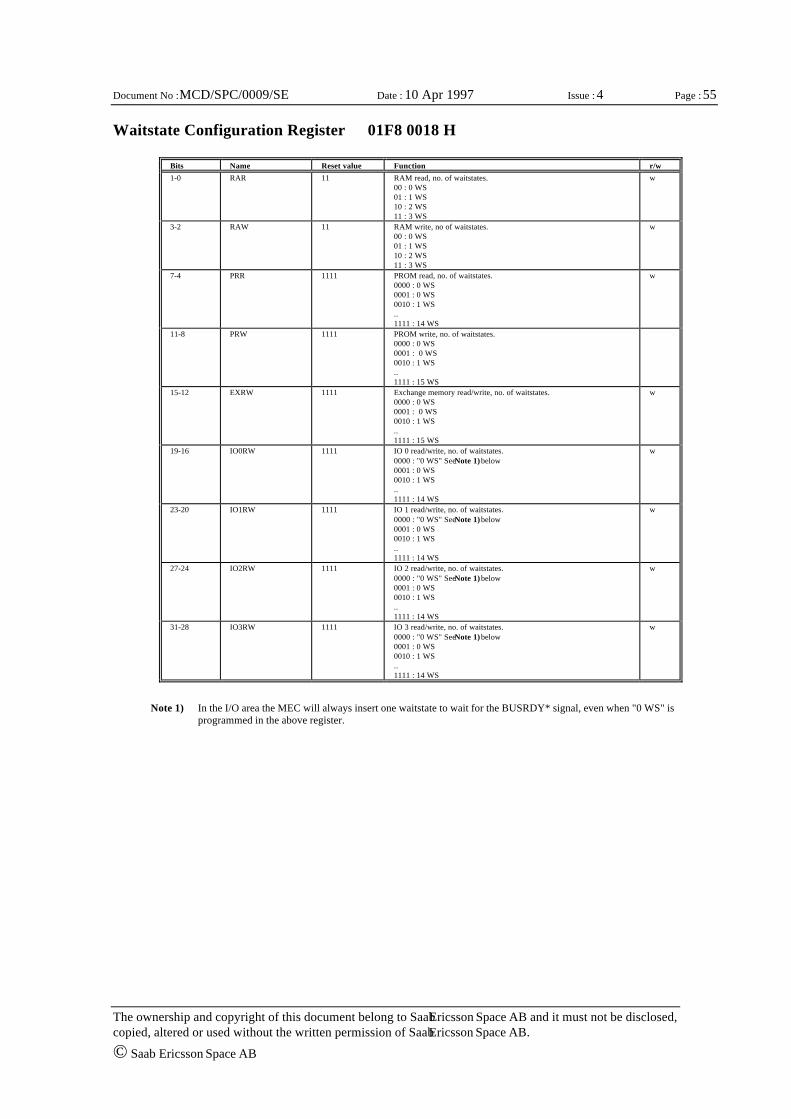
Page : 55
The ownership and copyright of this document belong to Saab Ericsson Space AB and it must not be disclosed,copied, altered or used without the written permission of Saab Ericsson Space AB.
© Saab Ericsson Space AB
Document No : MCD/SPC/0009/SE Date : 10 Apr 1997 Issue : 4
Waitstate Configuration Register 01F8 0018 H
Bits Name Reset value Function r/w1-0 RAR 11 RAM read, no. of waitstates.
00 : 0 WS01 : 1 WS10 : 2 WS11 : 3 WS
w
3-2 RAW 11 RAM write, no of waitstates.00 : 0 WS01 : 1 WS10 : 2 WS11 : 3 WS
w
7-4 PRR 1111 PROM read, no. of waitstates.0000 : 0 WS0001 : 0 WS0010 : 1 WS..1111 : 14 WS
w
11-8 PRW 1111 PROM write, no. of waitstates.0000 : 0 WS0001 : 0 WS0010 : 1 WS..1111 : 15 WS
15-12 EXRW 1111 Exchange memory read/write, no. of waitstates.0000 : 0 WS0001 : 0 WS0010 : 1 WS..1111 : 15 WS
w
19-16 IO0RW 1111 IO 0 read/write, no. of waitstates.0000 : "0 WS" See Note 1) below0001 : 0 WS0010 : 1 WS..1111 : 14 WS
w
23-20 IO1RW 1111 IO 1 read/write, no. of waitstates.0000 : "0 WS" See Note 1) below0001 : 0 WS0010 : 1 WS..1111 : 14 WS
w
27-24 IO2RW 1111 IO 2 read/write, no. of waitstates.0000 : "0 WS" See Note 1) below0001 : 0 WS0010 : 1 WS..1111 : 14 WS
w
31-28 IO3RW 1111 IO 3 read/write, no. of waitstates.0000 : "0 WS" See Note 1) below0001 : 0 WS0010 : 1 WS..1111 : 14 WS
w
Note 1) In the I/O area the MEC will always insert one waitstate to wait for the BUSRDY* signal, even when "0 WS" isprogrammed in the above register.
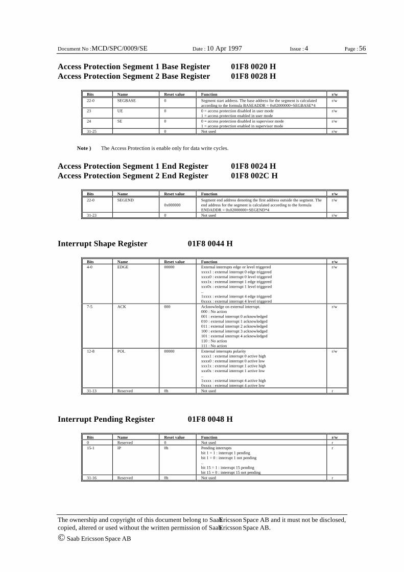
Page : 56
The ownership and copyright of this document belong to Saab Ericsson Space AB and it must not be disclosed,copied, altered or used without the written permission of Saab Ericsson Space AB.
© Saab Ericsson Space AB
Document No : MCD/SPC/0009/SE Date : 10 Apr 1997 Issue : 4
Access Protection Segment 1 Base Register 01F8 0020 HAccess Protection Segment 2 Base Register 01F8 0028 H
Bits Name Reset value Function r/w22-0 SEGBASE 0 Segment start address. The base address for the segment is calculated
according to the formula BASEADDR = 0x02000000+SEGBASE*4r/w
23 UE 0 0 = access protection disabled in user mode1 = access protection enabled in user mode
r/w
24 SE 0 0 = access protection disabled in supervisor mode1 = access protection enabled in supervisor mode
r/w
31-25 0 Not used r/w
Note ) The Access Protection is enable only for data write cycles.
Access Protection Segment 1 End Register 01F8 0024 HAccess Protection Segment 2 End Register 01F8 002C H
Bits Name Reset value Function r/w22-0 SEGEND
0x000000Segment end address denoting the first address outside the segment. Theend address for the segment is calculated according to the formulaENDADDR = 0x02000000+SEGEND*4
r/w
31-23 0 Not used r/w
Interrupt Pending Register 01F8 0048 H
Bits Name Reset value Function r/w0 Reserved 0 Not used r15-1 IP 0h Pending interrupts
bit 1 = 1 : interrupt 1 pendingbit 1 = 0 : interrupt 1 not pending..bit 15 = 1 : interrupt 15 pendingbit 15 = 0 : interrupt 15 not pending
r
31-16 Reserved 0h Not used r
Interrupt Shape Register 01F8 0044 H
Bits Name Reset value Function r/w4-0 EDGE 00000 External interrupts edge or level triggered
xxxx1 : external interrupt 0 edge triggeredxxxx0 : external interrupt 0 level triggeredxxx1x : external interrupt 1 edge triggeredxxx0x : external interrupt 1 level triggered..1xxxx : external interrupt 4 edge triggered0xxxx : external interrupt 4 level triggered
r/w
7-5 ACK 000 Acknowledge on external interrupt.000 : No action001 : external interrupt 0 acknowledged010 : external interrupt 1 acknowledged011 : external interrupt 2 acknowledged100 : external interrupt 3 acknowledged101 : external interrupt 4 acknowledged110 : No action111 : No action
r/w
12-8 POL 00000 External interrupts polarityxxxx1 : external interrupt 0 active highxxxx0 : external interrupt 0 active lowxxx1x : external interrupt 1 active highxxx0x : external interrupt 1 active low..1xxxx : external interrupt 4 active high0xxxx : external interrupt 4 active low
r/w
31-13 Reserved 0h Not used r
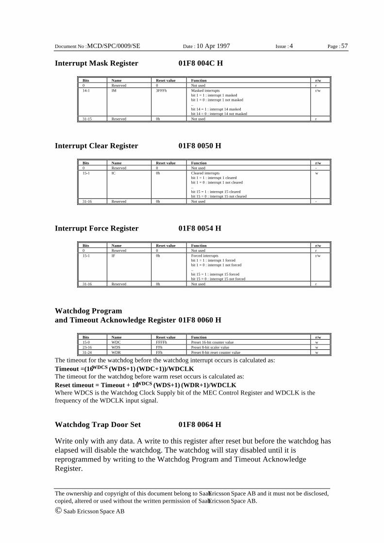
Page : 57
The ownership and copyright of this document belong to Saab Ericsson Space AB and it must not be disclosed,copied, altered or used without the written permission of Saab Ericsson Space AB.
© Saab Ericsson Space AB
Document No : MCD/SPC/0009/SE Date : 10 Apr 1997 Issue : 4
Interrupt Clear Register 01F8 0050 H
Bits Name Reset value Function r/w0 Reserved 0 Not used -15-1 IC 0h Cleared interrupts
bit 1 = 1 : interrupt 1 clearedbit 1 = 0 : interrupt 1 not cleared..bit 15 = 1 : interrupt 15 clearedbit 15 = 0 : interrupt 15 not cleared
w
31-16 Reserved 0h Not used -
Interrupt Force Register 01F8 0054 H
Bits Name Reset value Function r/w0 Reserved 0 Not used r15-1 IF 0h Forced interrupts
bit 1 = 1 : interrupt 1 forcedbit 1 = 0 : interrupt 1 not forced..bit 15 = 1 : interrupt 15 forcedbit 15 = 0 : interrupt 15 not forced
r/w
31-16 Reserved 0h Not used r
Watchdog Trap Door Set 01F8 0064 H
Write only with any data. A write to this register after reset but before the watchdog haselapsed will disable the watchdog. The watchdog will stay disabled until it isreprogrammed by writing to the Watchdog Program and Timeout AcknowledgeRegister.
Interrupt Mask Register 01F8 004C H
Bits Name Reset value Function r/w0 Reserved 0 Not used r14-1 IM 3FFFh Masked interrupts
bit 1 = 1 : interrupt 1 maskedbit 1 = 0 : interrupt 1 not masked..bit 14 = 1 : interrupt 14 maskedbit 14 = 0 : interrupt 14 not masked
r/w
31-15 Reserved 0h Not used r
Watchdog Programand Timeout Acknowledge Register 01F8 0060 H
Bits Name Reset value Function r/w15-0 WDC FFFFh Preset 16-bit counter value w23-16 WDS FFh Preset 8-bit scaler value w31-24 WDR FFh Preset 8-bit reset counter value w
The timeout for the watchdog before the watchdog interrupt occurs is calculated as:Timeout =(16WDCS⋅⋅(WDS+1)⋅⋅(WDC+1))/WDCLKThe timeout for the watchdog before warm reset occurs is calculated as:Reset timeout = Timeout + 16WDCS⋅⋅(WDS+1)⋅⋅(WDR+1)/WDCLKWhere WDCS is the Watchdog Clock Supply bit of the MEC Control Register and WDCLK is thefrequency of the WDCLK input signal.
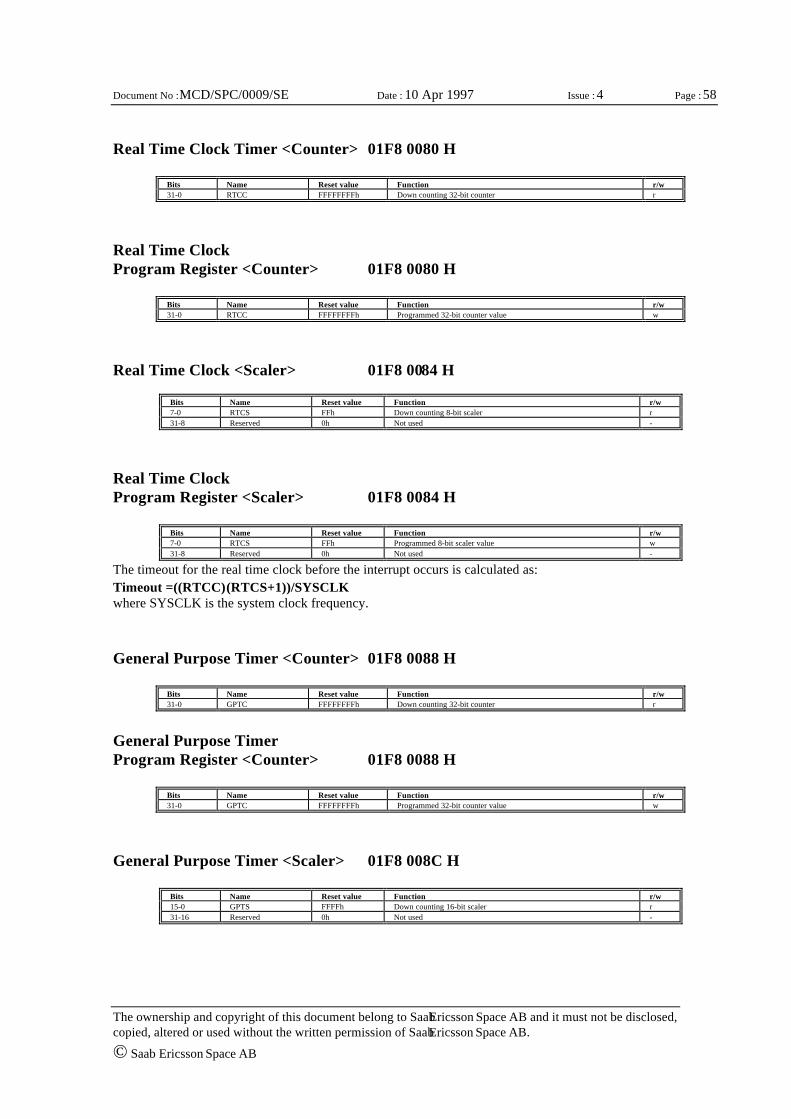
Page : 58
The ownership and copyright of this document belong to Saab Ericsson Space AB and it must not be disclosed,copied, altered or used without the written permission of Saab Ericsson Space AB.
© Saab Ericsson Space AB
Document No : MCD/SPC/0009/SE Date : 10 Apr 1997 Issue : 4
General Purpose TimerProgram Register <Counter> 01F8 0088 H
Bits Name Reset value Function r/w31-0 GPTC FFFFFFFFh Programmed 32-bit counter value w
General Purpose Timer <Scaler> 01F8 008C H
Bits Name Reset value Function r/w15-0 GPTS FFFFh Down counting 16-bit scaler r31-16 Reserved 0h Not used -
Real Time Clock Timer <Counter> 01F8 0080 H
Bits Name Reset value Function r/w31-0 RTCC FFFFFFFFh Down counting 32-bit counter r
Real Time ClockProgram Register <Counter> 01F8 0080 H
Bits Name Reset value Function r/w31-0 RTCC FFFFFFFFh Programmed 32-bit counter value w
Real Time Clock <Scaler> 01F8 0084 H
Bits Name Reset value Function r/w7-0 RTCS FFh Down counting 8-bit scaler r31-8 Reserved 0h Not used -
Real Time ClockProgram Register <Scaler> 01F8 0084 H
Bits Name Reset value Function r/w7-0 RTCS FFh Programmed 8-bit scaler value w31-8 Reserved 0h Not used -
The timeout for the real time clock before the interrupt occurs is calculated as:Timeout =((RTCC)⋅⋅(RTCS+1))/SYSCLKwhere SYSCLK is the system clock frequency.
General Purpose Timer <Counter> 01F8 0088 H
Bits Name Reset value Function r/w31-0 GPTC FFFFFFFFh Down counting 32-bit counter r
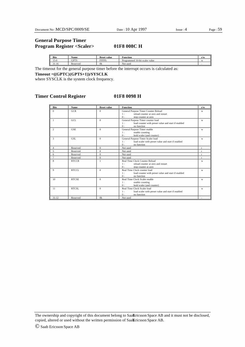
Page : 59
The ownership and copyright of this document belong to Saab Ericsson Space AB and it must not be disclosed,copied, altered or used without the written permission of Saab Ericsson Space AB.
© Saab Ericsson Space AB
Document No : MCD/SPC/0009/SE Date : 10 Apr 1997 Issue : 4
General Purpose TimerProgram Register <Scaler> 01F8 008C H
Bits Name Reset value Function r/w15-0 GPTS FFFFh Programmed 16-bit scaler value w31-16 Reserved 0h Not used -
The timeout for the general purpose timer before the interrupt occurs is calculated as:Timeout =((GPTC)⋅⋅(GPTS+1))/SYSCLKwhere SYSCLK is the system clock frequency.
Timer Control Register 01F8 0098 H
Bits Name Reset value Function r/w0 GCR 0 General Purpose Timer Counter Reload
1 : reload counter at zero and restart0 : stop counter at zero
w
1 GCL 0 General Purpose Timer counter load1 : load counter with preset value and start if enabled0 : no function
w
2 GSE 0 General Purpose Timer enable1 : enable counting0 : hold scaler (and counter)
w
3 GSL 0 General Purpose Timer Scaler load1 : load scaler with preset value and start if enabled0 : no function
w
4 Reserved 0 Not used r5 Reserved 0 Not used r6 Reserved 0 Not used r7 Reserved 0 Not used r8 RTCCR 1 Real Time Clock Counter Reload
1 : reload counter at zero and restart0 : stop counter at zero
w
9 RTCCL 0 Real Time Clock counter load1 : load counter with preset value and start if enabled0 : no function
w
10 RTCSE 0 Real Time Clock Scaler enable1 : enable counting0 : hold scaler (and counter)
w
11 RTCSL 0 Real Time Clock Scaler load1 : load scaler with preset value and start if enabled0 : no function
w
31-12 Reserved 0h Not used -
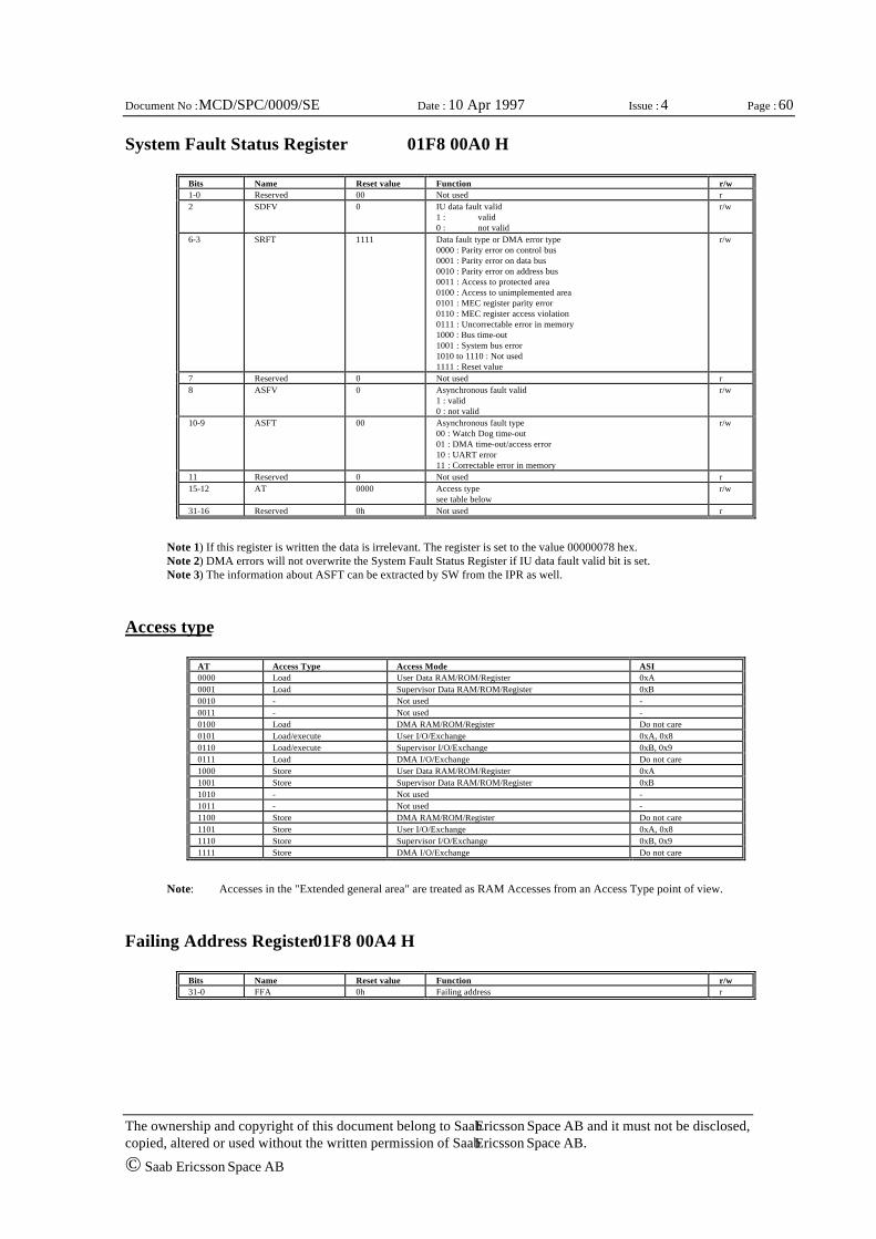
Page : 60
The ownership and copyright of this document belong to Saab Ericsson Space AB and it must not be disclosed,copied, altered or used without the written permission of Saab Ericsson Space AB.
© Saab Ericsson Space AB
Document No : MCD/SPC/0009/SE Date : 10 Apr 1997 Issue : 4
System Fault Status Register 01F8 00A0 H
Bits Name Reset value Function r/w1-0 Reserved 00 Not used r2 SDFV 0 IU data fault valid
1 : valid0 : not valid
r/w
6-3 SRFT 1111 Data fault type or DMA error type0000 : Parity error on control bus0001 : Parity error on data bus0010 : Parity error on address bus0011 : Access to protected area0100 : Access to unimplemented area0101 : MEC register parity error0110 : MEC register access violation0111 : Uncorrectable error in memory1000 : Bus time-out1001 : System bus error1010 to 1110 : Not used1111 : Reset value
r/w
7 Reserved 0 Not used r8 ASFV 0 Asynchronous fault valid
1 : valid0 : not valid
r/w
10-9 ASFT 00 Asynchronous fault type00 : Watch Dog time-out01 : DMA time-out/access error10 : UART error11 : Correctable error in memory
r/w
11 Reserved 0 Not used r15-12 AT 0000 Access type
see table belowr/w
31-16 Reserved 0h Not used r
Note 1) If this register is written the data is irrelevant. The register is set to the value 00000078 hex.Note 2) DMA errors will not overwrite the System Fault Status Register if IU data fault valid bit is set.Note 3) The information about ASFT can be extracted by SW from the IPR as well.
Access type
AT Access Type Access Mode ASI0000 Load User Data RAM/ROM/Register 0xA0001 Load Supervisor Data RAM/ROM/Register 0xB0010 - Not used -0011 - Not used -0100 Load DMA RAM/ROM/Register Do not care0101 Load/execute User I/O/Exchange 0xA, 0x80110 Load/execute Supervisor I/O/Exchange 0xB, 0x90111 Load DMA I/O/Exchange Do not care1000 Store User Data RAM/ROM/Register 0xA1001 Store Supervisor Data RAM/ROM/Register 0xB1010 - Not used -1011 - Not used -1100 Store DMA RAM/ROM/Register Do not care1101 Store User I/O/Exchange 0xA, 0x81110 Store Supervisor I/O/Exchange 0xB, 0x91111 Store DMA I/O/Exchange Do not care
Note: Accesses in the "Extended general area" are treated as RAM Accesses from an Access Type point of view.
Failing Address Register01F8 00A4 H
Bits Name Reset value Function r/w31-0 FFA 0h Failing address r

Page : 61
The ownership and copyright of this document belong to Saab Ericsson Space AB and it must not be disclosed,copied, altered or used without the written permission of Saab Ericsson Space AB.
© Saab Ericsson Space AB
Document No : MCD/SPC/0009/SE Date : 10 Apr 1997 Issue : 4
Error and Reset Status Register 01F8 00B0 H
Bits Name Reset value Function r/w0 IUEM 0 IU error mode
1 : error0 : no error
r/w
1 IUHE 0 IU hardware error1 : error0 : no error
r/w
2 IUCMP 0 IU comparison error1 : error0 : no error
r/w
3 FPUHE 0 FPU hardware error (no MEC action)1 : error0 : no error
r/w
4 FPUCMP 0 FPU comparison error1 : error0 : no error
r/w
5 MECHE 0 MEC hardware error.1 : Internal parity error0 : no error
r/w
11 - 6 0 Not used r/w12 SYSAV 0 ERC32 System availability
1 : System available0 : System not available
r/w
13 HLT 0 IU/FPU halted1 : active0 : not active
r
15-14 RSTCxx
Reset cause.00 : system reset01 : software reset10 : error reset11 : watchdog reset
r
31-16 Reserved 0h Not used r
Note: Bit 5-0 are only writeable when the EWE bit in the Test Control Register is set
Test Control Register 01F8 00D0 H
Bits Name Reset value Function r/w6-0 CB 0 Check bits r/w16-7 0 Not used r17 ET 0 EDAC test enable
0: Testing disabled1: Memory test enabled
r/w
18 PT 0 Parity test1 : test enabled0 : test disabled
r/w
19 IT 0 Interrupt Force Register Write Enable1 : enabled0 : disabled
r/w
20 EWE 0 Error Write Enable1: Write to Error and Reset Status Register enabled0: Write to Error and Reset Status Register disabled
r/w
31-21 0 Not used r
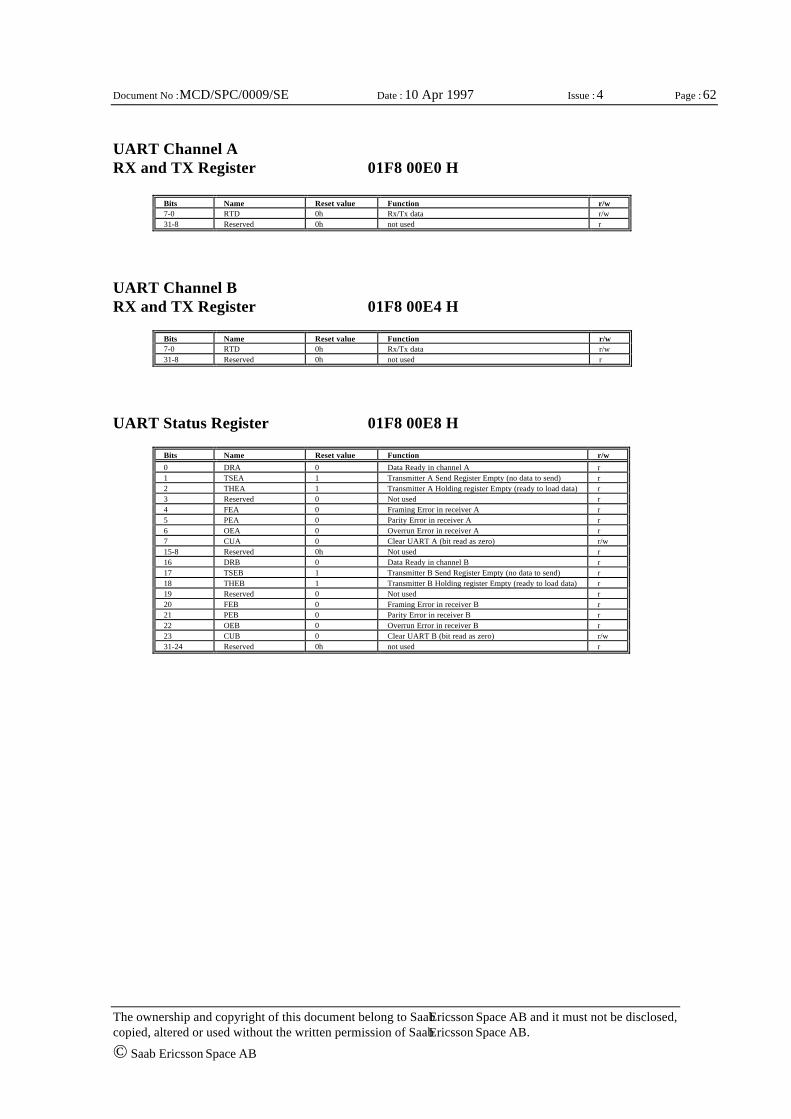
Page : 62
The ownership and copyright of this document belong to Saab Ericsson Space AB and it must not be disclosed,copied, altered or used without the written permission of Saab Ericsson Space AB.
© Saab Ericsson Space AB
Document No : MCD/SPC/0009/SE Date : 10 Apr 1997 Issue : 4
UART Channel ARX and TX Register 01F8 00E0 H
Bits Name Reset value Function r/w7-0 RTD 0h Rx/Tx data r/w31-8 Reserved 0h not used r
UART Channel BRX and TX Register 01F8 00E4 H
Bits Name Reset value Function r/w7-0 RTD 0h Rx/Tx data r/w31-8 Reserved 0h not used r
UART Status Register 01F8 00E8 H
Bits Name Reset value Function r/w0 DRA 0 Data Ready in channel A r1 TSEA 1 Transmitter A Send Register Empty (no data to send) r2 THEA 1 Transmitter A Holding register Empty (ready to load data) r3 Reserved 0 Not used r4 FEA 0 Framing Error in receiver A r5 PEA 0 Parity Error in receiver A r6 OEA 0 Overrun Error in receiver A r7 CUA 0 Clear UART A (bit read as zero) r/w15-8 Reserved 0h Not used r16 DRB 0 Data Ready in channel B r17 TSEB 1 Transmitter B Send Register Empty (no data to send) r18 THEB 1 Transmitter B Holding register Empty (ready to load data) r19 Reserved 0 Not used r20 FEB 0 Framing Error in receiver B r21 PEB 0 Parity Error in receiver B r22 OEB 0 Overrun Error in receiver B r23 CUB 0 Clear UART B (bit read as zero) r/w31-24 Reserved 0h not used r
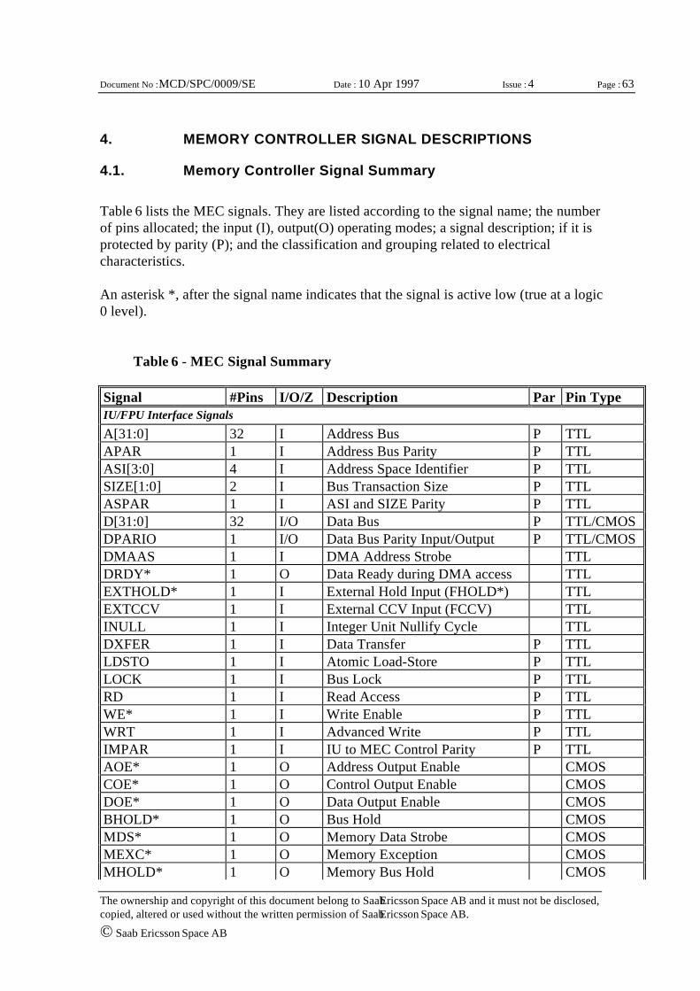
Page : 63
The ownership and copyright of this document belong to Saab Ericsson Space AB and it must not be disclosed,copied, altered or used without the written permission of Saab Ericsson Space AB.
© Saab Ericsson Space AB
Document No : MCD/SPC/0009/SE Date : 10 Apr 1997 Issue : 4
4. MEMORY CONTROLLER SIGNAL DESCRIPTIONS
4.1. Memory Controller Signal Summary
Table 6 lists the MEC signals. They are listed according to the signal name; the numberof pins allocated; the input (I), output(O) operating modes; a signal description; if it isprotected by parity (P); and the classification and grouping related to electricalcharacteristics.
An asterisk *, after the signal name indicates that the signal is active low (true at a logic0 level).
Table 6 - MEC Signal Summary
Signal #Pins I/O/Z Description Par Pin TypeIU/FPU Interface Signals
A[31:0] 32 I Address Bus P TTLAPAR 1 I Address Bus Parity P TTLASI[3:0] 4 I Address Space Identifier P TTLSIZE[1:0] 2 I Bus Transaction Size P TTLASPAR 1 I ASI and SIZE Parity P TTLD[31:0] 32 I/O Data Bus P TTL/CMOSDPARIO 1 I/O Data Bus Parity Input/Output P TTL/CMOSDMAAS 1 I DMA Address Strobe TTLDRDY* 1 O Data Ready during DMA access TTLEXTHOLD* 1 I External Hold Input (FHOLD*) TTLEXTCCV 1 I External CCV Input (FCCV) TTLINULL 1 I Integer Unit Nullify Cycle TTLDXFER 1 I Data Transfer P TTLLDSTO 1 I Atomic Load-Store P TTLLOCK 1 I Bus Lock P TTLRD 1 I Read Access P TTLWE* 1 I Write Enable P TTLWRT 1 I Advanced Write P TTLIMPAR 1 I IU to MEC Control Parity P TTLAOE* 1 O Address Output Enable CMOSCOE* 1 O Control Output Enable CMOSDOE* 1 O Data Output Enable CMOSBHOLD* 1 O Bus Hold CMOSMDS* 1 O Memory Data Strobe CMOSMEXC* 1 O Memory Exception CMOSMHOLD* 1 O Memory Bus Hold CMOS
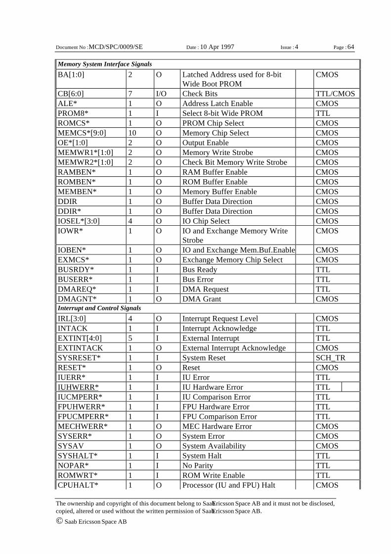
Page : 64
The ownership and copyright of this document belong to Saab Ericsson Space AB and it must not be disclosed,copied, altered or used without the written permission of Saab Ericsson Space AB.
© Saab Ericsson Space AB
Document No : MCD/SPC/0009/SE Date : 10 Apr 1997 Issue : 4
Memory System Interface Signals
BA[1:0] 2 O Latched Address used for 8-bitWide Boot PROM
CMOS
CB[6:0] 7 I/O Check Bits TTL/CMOSALE* 1 O Address Latch Enable CMOSPROM8* 1 I Select 8-bit Wide PROM TTLROMCS* 1 O PROM Chip Select CMOSMEMCS*[9:0] 10 O Memory Chip Select CMOSOE*[1:0] 2 O Output Enable CMOSMEMWR1*[1:0] 2 O Memory Write Strobe CMOSMEMWR2*[1:0] 2 O Check Bit Memory Write Strobe CMOSRAMBEN* 1 O RAM Buffer Enable CMOSROMBEN* 1 O ROM Buffer Enable CMOSMEMBEN* 1 O Memory Buffer Enable CMOSDDIR 1 O Buffer Data Direction CMOSDDIR* 1 O Buffer Data Direction CMOSIOSEL*[3:0] 4 O IO Chip Select CMOSIOWR* 1 O IO and Exchange Memory Write
StrobeCMOS
IOBEN* 1 O IO and Exchange Mem.Buf.Enable CMOSEXMCS* 1 O Exchange Memory Chip Select CMOSBUSRDY* 1 I Bus Ready TTLBUSERR* 1 I Bus Error TTLDMAREQ* 1 I DMA Request TTLDMAGNT* 1 O DMA Grant CMOSInterrupt and Control Signals
IRL[3:0] 4 O Interrupt Request Level CMOSINTACK 1 I Interrupt Acknowledge TTLEXTINT[4:0] 5 I External Interrupt TTLEXTINTACK 1 O External Interrupt Acknowledge CMOSSYSRESET* 1 I System Reset SCH_TRRESET* 1 O Reset CMOSIUERR* 1 I IU Error TTLIUHWERR* 1 I IU Hardware Error TTLIUCMPERR* 1 I IU Comparison Error TTLFPUHWERR* 1 I FPU Hardware Error TTLFPUCMPERR* 1 I FPU Comparison Error TTLMECHWERR* 1 O MEC Hardware Error CMOSSYSERR* 1 O System Error CMOSSYSAV 1 O System Availability CMOSSYSHALT* 1 I System Halt TTLNOPAR* 1 I No Parity TTLROMWRT* 1 I ROM Write Enable TTLCPUHALT* 1 O Processor (IU and FPU) Halt CMOS
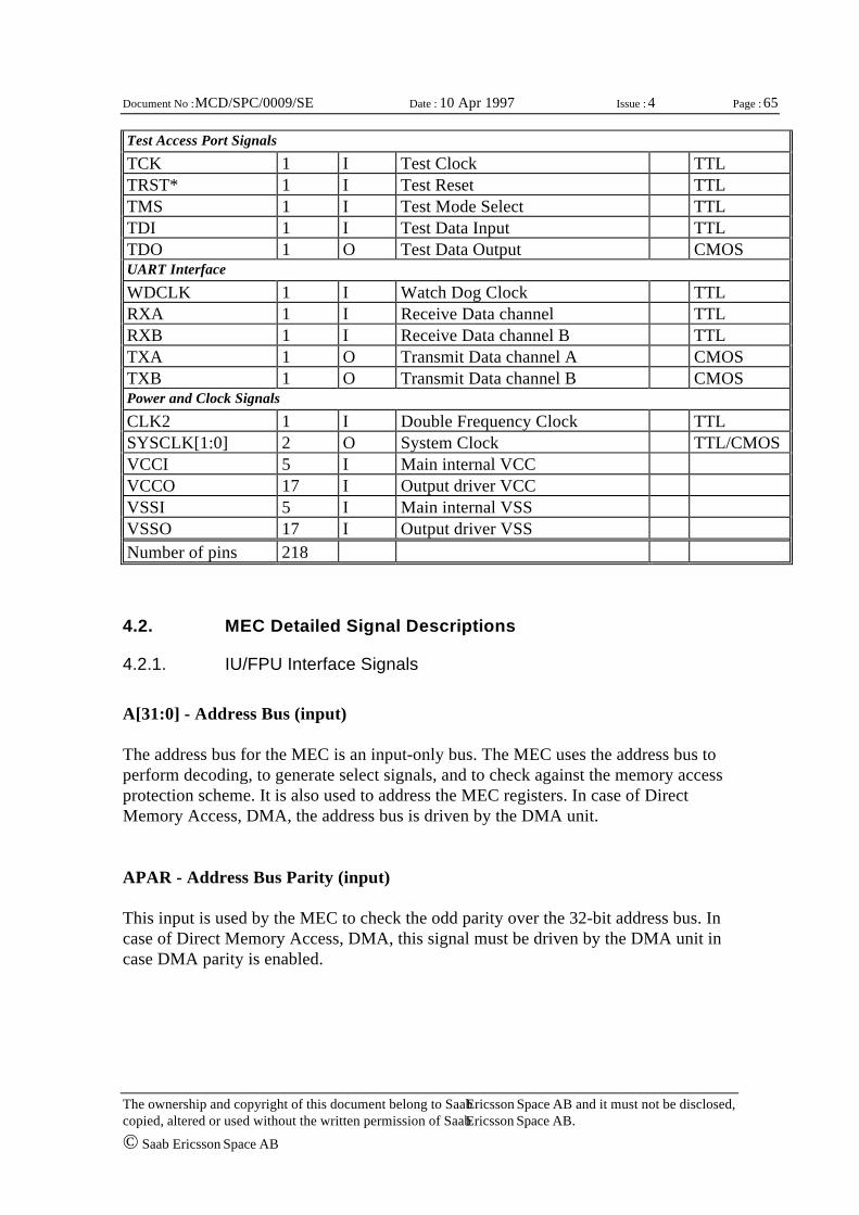
Page : 65
The ownership and copyright of this document belong to Saab Ericsson Space AB and it must not be disclosed,copied, altered or used without the written permission of Saab Ericsson Space AB.
© Saab Ericsson Space AB
Document No : MCD/SPC/0009/SE Date : 10 Apr 1997 Issue : 4
Test Access Port Signals
TCK 1 I Test Clock TTLTRST* 1 I Test Reset TTLTMS 1 I Test Mode Select TTLTDI 1 I Test Data Input TTLTDO 1 O Test Data Output CMOSUART Interface
WDCLK 1 I Watch Dog Clock TTLRXA 1 I Receive Data channel TTLRXB 1 I Receive Data channel B TTLTXA 1 O Transmit Data channel A CMOSTXB 1 O Transmit Data channel B CMOSPower and Clock Signals
CLK2 1 I Double Frequency Clock TTLSYSCLK[1:0] 2 O System Clock TTL/CMOSVCCI 5 I Main internal VCCVCCO 17 I Output driver VCCVSSI 5 I Main internal VSSVSSO 17 I Output driver VSSNumber of pins 218
4.2. MEC Detailed Signal Descriptions
4.2.1. IU/FPU Interface Signals
A[31:0] - Address Bus (input)
The address bus for the MEC is an input-only bus. The MEC uses the address bus toperform decoding, to generate select signals, and to check against the memory accessprotection scheme. It is also used to address the MEC registers. In case of DirectMemory Access, DMA, the address bus is driven by the DMA unit.
APAR - Address Bus Parity (input)
This input is used by the MEC to check the odd parity over the 32-bit address bus. Incase of Direct Memory Access, DMA, this signal must be driven by the DMA unit incase DMA parity is enabled.
Page : 66
The ownership and copyright of this document belong to Saab Ericsson Space AB and it must not be disclosed,copied, altered or used without the written permission of Saab Ericsson Space AB.
© Saab Ericsson Space AB
Document No : MCD/SPC/0009/SE Date : 10 Apr 1997 Issue : 4
ASI[3:0] - Address Space Identifier (input)
These four bits constitute the Address Space Identifier (ASI), which identifies thememory address space to which the memory access is being directed. The ASI bits arelatched by the MEC and are used to detect supervisor mode, instruction or data access,etc. A DMA unit must supply these bits.
SIZE[1:0] - Bus Transaction Size (input)
The coding on these pins specifies for the MEC the size of the data being transferredduring a memory access. A DMA unit must drive these bits to '10', since only wordtransfers are allowed in DMA mode.
ASPAR - ASI and SIZE Parity (input)
This input is used by the MEC to check the odd parity over the ASI[3:0] and theSIZE[1:0] signals. A DMA unit must supply this bit in case DMA parity is enabled. Notethat although ASI[7:0] exist in the IU, only ASI[3:0] are connected to the MEC. Thismeans that from the IU, only alternate address space accesses with ASI[7:4] containing0, 2 or 4 ones may be used (ASI[7:4] = 0000, 0011, 0101, 0110, 1001, 1010, 1100 or1111), otherwise an ASI and SIZE parity error will be detected in the MEC, as the IUcomputes ASPAR over the full ASI[7:0] range.
D[31:0] - Data Bus (bi-directional)
These pins form a 32-bit bi-directional data bus that serves as the interface between theIU and the MEC. It is driven by the MEC only during read of its internal registers, whenreading the boot PROM in 8-bit mode, and when a single bit error is detected by theEDAC. When implementing a system with an 8-bit PROM, the PROM shall beconnected to bits D[7:0]. In case of Direct Memory Access, DMA, it is driven or read bythe DMA unit.
DPARIO - Data Bus Parity Input/Output (bi-directional)
This pin is used by the MEC to check and generate the odd parity over the 32-bit databus during write cycles. A DMA unit must supply this bit in case DMA parity is enabled.See also Table 4 on page 33.
Page : 67
The ownership and copyright of this document belong to Saab Ericsson Space AB and it must not be disclosed,copied, altered or used without the written permission of Saab Ericsson Space AB.
© Saab Ericsson Space AB
Document No : MCD/SPC/0009/SE Date : 10 Apr 1997 Issue : 4
DMAAS - DMA Address Strobe (input)
During DMA transfers (when the external DMA is bus master) this input is used toinform the MEC that the address from the DMA is valid and that the access cycle shallstart. DMAAS can be asserted multiple times during DMA grant.
DRDY* - Data Ready during DMA access (output)
During DMA read transfers (when the external DMA is bus master) this output is usedto inform the DMA unit that the data are valid. During DMA write transfers this signalindicates that data have been written into memory.
INULL - Integer Unit Nullify Cycle (input)
INULL is output from the IU to indicate that the current memory access is nullified. Seefurther the IU signal description.
ExtHOLD* - External unit Hold (input)
This signal input is used to synchronize coprocessor compare instructions with branchinstructions. The MEC shall use this signal for prolonging of ongoing cycle. See furtherthe FPU FHold / CHold signal description.
ExtCCV - External unit Condition Codes Valid (input)
This signal input is used to hold the MEC when a coprocessor can not continueexecution. The MEC shall use this signal for prolonging of ongoing cycle. See further theFPU FCCV / CCCV signal description.
DXFER - Data Transfer (input)
DXFER is used to differentiate between the addresses being sent out for instructionfetches and the addresses of data fetches. DXFER is asserted by the processor during theaddress cycles of all bus data transfer cycles, including both cycles of store single and allthree cycles of store double and atomic load-store. DXFER is sent out unlatched and islatched in the MEC before it is used. A DMA unit must supply this signal during a DMAsession.
Page : 68
The ownership and copyright of this document belong to Saab Ericsson Space AB and it must not be disclosed,copied, altered or used without the written permission of Saab Ericsson Space AB.
© Saab Ericsson Space AB
Document No : MCD/SPC/0009/SE Date : 10 Apr 1997 Issue : 4
LDSTO - Atomic Load-Store (input)
This signal is used to identify an atomic load-store to the system and is asserted by theinteger unit during all the data cycles (the load cycle and both store cycles) of atomicload-store instructions. LDSTO is sent out unlatched and is latched in the MEC before itis used. A DMA unit must supply this signal during a DMA session.
LOCK -Bus Lock (input)
LOCK is asserted by the processor when it needs to retain control of the bus (addressand data) for multiple cycle transactions (Load Double, Store Single and Double, AtomicLoad-Store). The bus will not be granted to another bus master as long as LOCK isasserted. Note that BHOLD* should not be asserted in the processor clock cycle whichfollows a cycle in which LOCK is asserted. LOCK is sent out unlatched and must belatched externally before it is used. A DMA unit must supply this signal during a DMAsession.
RD - Read Access (input)
RD is used in conjunction with SIZE[1:0], ASI[3:0] and LDSTO to determine the typeof transfer and to check the write access rights of bus transactions. It may also be used toturn off the output drivers of data RAMs during a store operation. A DMA unit mustsupply this signal during a DMA session, deasserted low for write and asserted high forread accesses.
WE* - Write Enable (input)
WE* is asserted by the integer unit during the cycle in which the store data is on the databus. For a store single instruction, this is during the second store address cycle; thesecond and third store address cycles of store double instructions, and the third load-store address cycle of atomic load-store instructions. It is sent out unlatched and islatched in the MEC before it is used. To avoid writing to memory during memoryexceptions, WE* is internally qualified by MHOLD* and MEXC*. A DMA unit mustsupply this signal during a DMA session, asserted low for write and deasserted high forread accesses.
Page : 69
The ownership and copyright of this document belong to Saab Ericsson Space AB and it must not be disclosed,copied, altered or used without the written permission of Saab Ericsson Space AB.
© Saab Ericsson Space AB
Document No : MCD/SPC/0009/SE Date : 10 Apr 1997 Issue : 4
WRT - Advanced Write (input)
WRT is an early write signal, asserted by the processor during the first store addresscycle of integer single or double store instructions, the first store address cycle offloating-point single or double store instructions, and the second load-store address cycleof atomic load-store instructions. WRT is sent out unlatched and is latched in the MECbefore it is used. A DMA unit must supply this signal during a DMA session, deassertedlow for read and asserted high for write accesses.
IMPAR - IU to MEC Control Parity (input)
This input is used by the MEC to check the odd parity over the LDSTO, DXFER,LOCK, WRT, RD, and WE* signals. This signal must be driven by the DMA if DMAuses parity.
AOE* - Address Output Enable (output)
The MEC deasserts this signal when an external master (DMA unit) uses the addressbus.
COE* - Control Output Enable (output)
The MEC deasserts this signal when an external master (DMA unit) uses the control bus.
DOE* - Data Output Enable (output)
The MEC deasserts this signal when an external master (DMA unit) uses the data bus.
BHOLD* - Bus Hold (output)
The MEC asserts this signal during DMA accesses.
MDS* - Memory Data Strobe (output)
During nominal execution with the IU as bus master, MDS* is asserted by the MEC toenable the clock to the instruction register of the IU (during an instruction fetch) or tothe load result register (during a data fetch) while the pipeline is frozen with anMHOLDA/B*.
Page : 70
The ownership and copyright of this document belong to Saab Ericsson Space AB and it must not be disclosed,copied, altered or used without the written permission of Saab Ericsson Space AB.
© Saab Ericsson Space AB
Document No : MCD/SPC/0009/SE Date : 10 Apr 1997 Issue : 4
MEXC* - Memory Exception (output)
Assertion of this signal by the MEC initiates an instruction access exception or dataaccess exception trap and indicates to the IU that the memory system was unable tosupply a valid instruction or data. It is asserted when a parity error, uncorrectable EDACerror, access violation, bus time-out or system bus error is detected. If this signal isasserted during a DMA transfer, the DMA must withdraw its DMA request and end theDMA cycle.
MHOLD* - Memory Bus Hold (output)
MHOLD* is used to freeze the clock to both the IU and floating-point unit during acache miss (for systems with cache memory) or when accessing a slow memory. It isgenerated by the MEC to insert wait states during memory or I/O accesses.
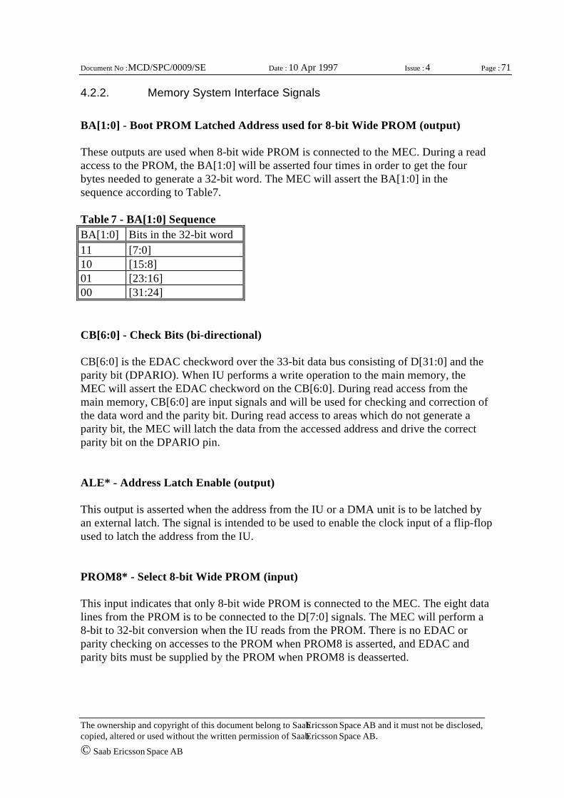
Page : 71
The ownership and copyright of this document belong to Saab Ericsson Space AB and it must not be disclosed,copied, altered or used without the written permission of Saab Ericsson Space AB.
© Saab Ericsson Space AB
Document No : MCD/SPC/0009/SE Date : 10 Apr 1997 Issue : 4
4.2.2. Memory System Interface Signals
BA[1:0] - Boot PROM Latched Address used for 8-bit Wide PROM (output)
These outputs are used when 8-bit wide PROM is connected to the MEC. During a readaccess to the PROM, the BA[1:0] will be asserted four times in order to get the fourbytes needed to generate a 32-bit word. The MEC will assert the BA[1:0] in thesequence according to Table 7.
Table 7 - BA[1:0] SequenceBA[1:0] Bits in the 32-bit word11 [7:0]10 [15:8]01 [23:16]00 [31:24]
CB[6:0] - Check Bits (bi-directional)
CB[6:0] is the EDAC checkword over the 33-bit data bus consisting of D[31:0] and theparity bit (DPARIO). When IU performs a write operation to the main memory, theMEC will assert the EDAC checkword on the CB[6:0]. During read access from themain memory, CB[6:0] are input signals and will be used for checking and correction ofthe data word and the parity bit. During read access to areas which do not generate aparity bit, the MEC will latch the data from the accessed address and drive the correctparity bit on the DPARIO pin.
ALE* - Address Latch Enable (output)
This output is asserted when the address from the IU or a DMA unit is to be latched byan external latch. The signal is intended to be used to enable the clock input of a flip-flopused to latch the address from the IU.
PROM8* - Select 8-bit Wide PROM (input)
This input indicates that only 8-bit wide PROM is connected to the MEC. The eight datalines from the PROM is to be connected to the D[7:0] signals. The MEC will perform a8-bit to 32-bit conversion when the IU reads from the PROM. There is no EDAC orparity checking on accesses to the PROM when PROM8 is asserted, and EDAC andparity bits must be supplied by the PROM when PROM8 is deasserted.
Page : 72
The ownership and copyright of this document belong to Saab Ericsson Space AB and it must not be disclosed,copied, altered or used without the written permission of Saab Ericsson Space AB.
© Saab Ericsson Space AB
Document No : MCD/SPC/0009/SE Date : 10 Apr 1997 Issue : 4
ROMCS* - PROM Chip Select (output)
This output is asserted whenever there is an access to the PROM. It can be connecteddirectly to the PROM chip select pins.
MEMCS*[9:0] - Memory Chip Select (output)
MEMCS*[9:0] is asserted during an access to the main memory. MEMCS*[9:8] areredundant signals, used to substitute any of the nominal memory banks when memoryconnected to any of MEMCS*[7:0] malfunctions.
OE*[1:0] - Output Enable (output)
OE*[1:0] are asserted during read accesses to the main memory and is used to controlmemory devices with output enable features. Two signals are provided in order to avoidan external buffer, since a single OE* signal would be too heavily loaded in typicalsystem.
MEMWR1*[1:0] - Memory Write (output)
MEMWR1* is asserted during write access to RAM, extended RAM, boot PROMextended boot PROM. It is intended to be used as write strobe to the memory devices. Iflatching buffers are used for the data bus, this signal can be used as a strobe to latch thedata and the MEMWR2* signal can be used to write the data into the main memory.Two signals are provided in order to avoid an external buffer, since a single signal wouldbe too heavily loaded in typical system.
MEMWR2*[1:0] - Check Bit Write (output)
MEMWR2* is asserted during write access to RAM, extended RAM, boot PROMextended boot PROM and exchange memory. It is intended to be used as write strobe tocheck bit memory devices, if implemented. If latching buffers are used for the data bus,this signal can be used to write both the check bits into the check bit memory and thedata bits into the main memory. Two signals are provided in order to avoid an externalbuffer, since a single signal would be too heavily loaded in typical system.
RAMBEN* - RAM Buffer Enable (output)
RAMBEN* is asserted during memory accesses to RAM. It is intended to be used asbuffer enable for data and check bit buffers in the RAM.
Page : 73
The ownership and copyright of this document belong to Saab Ericsson Space AB and it must not be disclosed,copied, altered or used without the written permission of Saab Ericsson Space AB.
© Saab Ericsson Space AB
Document No : MCD/SPC/0009/SE Date : 10 Apr 1997 Issue : 4
ROMBEN* - Boot PROM Buffer Enable (output)
ROMBEN* is asserted during memory accesses to boot PROM. It is intended to be usedas buffer enable for data and check bit buffers in the boot PROM areas.
MEMBEN* - Memory Buffer Enable (output)
MEMBEN* is asserted during memory accesses to both RAM and boot PROM. It isintended to be used as buffer enable for data and check bit buffers in the RAM and bootPROM areas if RAM and boot PROM share the same buffers.
DDIR - Data Direction (output)
DDIR is used for determining the direction of the data buffers connected between thelocal ERC32 bus and the ERC32 system bus. The DDIR is asserted when the data flowsfrom the local bus to the system bus i.e. during write operations. It is valid during allmemory accesses.
DDIR* - Data Direction (output)
DDIR* is used for determining the direction of the data buffers connected between thelocal ERC32 bus and the ERC32 system bus. The DDIR* is asserted when the dataflows from the local bus to the system bus i.e. during write operations. It is valid duringall memory accesses.
IOSEL*[3:0] - IO Chip Select (output)
These four select signals are used to enable one of four possible I/O address areas.
IOWR* - IO Write (output)
IOWR* is asserted during write operations to the I/O area, extended I/O area and theexchange memory area.
IOBEN* - IO Buffer Enable (output)
IOBEN* is asserted during I/O access, extended I/O area extended general area andexchange memory access in order to enable the data buffers for the I/O and exchangememory.
Page : 74
The ownership and copyright of this document belong to Saab Ericsson Space AB and it must not be disclosed,copied, altered or used without the written permission of Saab Ericsson Space AB.
© Saab Ericsson Space AB
Document No : MCD/SPC/0009/SE Date : 10 Apr 1997 Issue : 4
EXMCS* - Exchange Memory Chip Select (output)
EXMCS* is asserted when the exchange memory is accessed.
BUSRDY* - Bus Ready (input)
BUSRDY* is to be generated by a unit in the I/O area, exchange memory area or in theextended areas, which requires extended time when accessed in addition to thepreprogrammed number of wait states. (Note however that waitstates can not bepreprogrammed for units in the extended general area, only for extended I/O, bootPROM and RAM)
BUSERR* - Bus Error (input)
BUSERR* is to be generated together with BUSRDY* by a unit in the I/O area,exchange memory area or in the extended areas if an error is detected by the accessedunit during an access.
DMAREQ* - DMA Request (input)
DMAREQ* is to be issued by a unit requesting the access to the processor bus as amaster.
DMAGNT* - DMA Grant (output)
DMAGNT* is generated by the MEC as a response to a DMAREQ*. DMAGNT* issent after that the MEC has asserted BHOLD* and deasserted AOE*, DOE*, and COE*for holding and three-stating the IU.
Page : 75
The ownership and copyright of this document belong to Saab Ericsson Space AB and it must not be disclosed,copied, altered or used without the written permission of Saab Ericsson Space AB.
© Saab Ericsson Space AB
Document No : MCD/SPC/0009/SE Date : 10 Apr 1997 Issue : 4
4.2.3. Interrupt and Control Signals
IRL[3:0] - Interrupt Request Level (output)
The state of these pins defines the Interrupt Request Level (IRL). IRL[3:0] = 0000indicates that no external interrupts are pending and is the normal state of the IRL pins.IRL[3:0] = 1111 signifies a nonmaskable interrupt. All other interrupt levels aremaskable by the Processor Interrupt Level (PIL) field of the Processor State Register(PSR). External interrupts are latched and prioritized by the MEC before they are passedto the IU.
INTACK - Interrupt Acknowledge (input)
INTACK is asserted by the IU when an external interrupt is taken, not when it issampled and latched. The MEC will clear the corresponding pending interrupt whenINTACK is asserted.
EXTINT[4:0] - External Interrupt (input)
The five external interrupt inputs are programmable to be level or edge sensitive, andactive high (rising) or active low (falling).
EXTINTACK - External Interrupt Acknowledge (output)
EXTINTACK is for giving acknowledge to an interrupting unit which requires such asignal. It is programmable to which of the five external interrupt input it is associated. Itis issued as soon as the IU has recognized the interrupt by asserting the INTACK signal.
SYSRESET* - System Reset (input)
Assertion of this pin will reset the MEC. Following this the MEC will then assertRESET* for a minimum of sixteen clock cycles. SYSRESET* must be asserted for aminimum of four clock cycles.
RESET* - Reset (output)
RESET* will be asserted when the IU and the FPU is to be synchronously reset. Thisoccurs when either SYSRESET* is asserted or the MEC initiate a reset due to an erroror a programming command.
Page : 76
The ownership and copyright of this document belong to Saab Ericsson Space AB and it must not be disclosed,copied, altered or used without the written permission of Saab Ericsson Space AB.
© Saab Ericsson Space AB
Document No : MCD/SPC/0009/SE Date : 10 Apr 1997 Issue : 4
IUERR* - IU Error (input)
This input is connected to the ERROR* output of the (master) IU and is asserted whenthe (master) IU enters error mode.
IUHWERR* - IU Hardware Error (input)
This input is connected to the HWERR* output of the (master) IU and is asserted whenthe IU detects an internal hardware error.
IUCMPERR* - IU Comparison Error (input)
This input is connected to the CMPERR* signal of the slave IU in a master/slaveconfiguration and is asserted when there is a comparison error.
FPUHWERR* - FPU Hardware Error (input)
This input is connected to the HWERROR* output of the (master) FPU and is assertedwhenever there is an error in the (master) FPU.
FPUCMPERR* - FPU Comparison Error (input)
This input is connected to the CMPERR* signal of the slave FPU in a master/slaveconfiguration and is asserted when there is a comparison error.
MECHWERR* - MEC Hardware Error (output)
MECHWERR is an output indicating that a hardware error has been detected in theMEC.
SYSERR* - System Error (output)
This output is asserted whenever an unmasked error is set in the ERSR register. It staysasserted until the ERSR is cleared. The error can originate from either the IU, the FPU,or the MEC itself. SYSERR* is used to signal to the system outside the ERC32 basedcomputer.
Page : 77
The ownership and copyright of this document belong to Saab Ericsson Space AB and it must not be disclosed,copied, altered or used without the written permission of Saab Ericsson Space AB.
© Saab Ericsson Space AB
Document No : MCD/SPC/0009/SE Date : 10 Apr 1997 Issue : 4
4.2.4. Test Access Port Signals
The following Test Access Port interface (IEEE standard 1149.1) is used to performboundary scan for test and debugging purposes.
SYSAV - System Availability (output)
This signal is asserted whenever the system is available, i.e. when the SYSAV bit in theERSR is set and the CPUHALT* and SYSERR* signals are deasserted. The SYSAV bitis cleared by reset and is programmable by software.
SYSHALT* - System Halt (input)
SYSHALT* is used by the system outside to halt the ERC32. By asserting this signal,the MEC will assert CPUHALT* halting the IU and the FPU. This signal could be usedfor testing through the DMA or the TAP interface.
NOPAR* - No Parity (input)
Assertion of this signal will disable the parity checking of all signals related to the ERC32local buses. The parity generation on the data bus (towards memory and IO units) is notaffected by this signal, but note that parity checking is disabled if NOPAR* is asserted.This is a static signal and shall not change when running.
ROMWRT* - ROM Write Enable (input)
Assertion of this signal will validate (allow) programming (write operations) of the bootPROM when EEPROM devices are used.
CPUHALT* - Processor (IU and FPU) Halt (output)
This output is intended to be connected to the HALT* inputs of the IU and of the FPUand is used to halt the IU, the FPU and possibly other units in the system.
TCK - Test Clock (input)
Test clock for scan registers.
Page : 78
The ownership and copyright of this document belong to Saab Ericsson Space AB and it must not be disclosed,copied, altered or used without the written permission of Saab Ericsson Space AB.
© Saab Ericsson Space AB
Document No : MCD/SPC/0009/SE Date : 10 Apr 1997 Issue : 4
4.2.5. UART Interface
TRST* - Test Reset (input)
Reset the TAP controller.
TMS - Test Mode Select (input)
Selects test mode of the TAP controller.
TDI - Test Data Input (input)
Test scan register data input.
TDO - Test Data Output (output)
Test scan register data output, not affected by MODE.
WDCLK - Watch Dog Clock (input)
WDCLK is the WD clock input but this clock can also be used as a clock input for theUART interface. The clock frequency of WDCLK must be less than the clock frequencyof SYSCLK, i.e. fWDCLK < fSYSCLK.
RXA - Receive Data channel A (input)
RXA is the serial data input for channel A of the UART.
RXB - Receive Data channel B (input)
RXB is the serial data input for channel B of the UART.
TXA - Transmit Data channel A (output)
TXA is the serial data output for channel A of the UART.
TXB - Transmit Data channel B (output)
TXB is the serial data output for channel B of the UART.
Page : 79
The ownership and copyright of this document belong to Saab Ericsson Space AB and it must not be disclosed,copied, altered or used without the written permission of Saab Ericsson Space AB.
© Saab Ericsson Space AB
Document No : MCD/SPC/0009/SE Date : 10 Apr 1997 Issue : 4
4.2.6. Power and Clock Signals
CLK2 - Double Frequency Clock (input)
CLK2 is the input clock to the ERC32 hardware. The frequency of this clock must betwice the clock frequency used to clock the IU and the FPU. Note that the externaltiming of the MEC is affected by the duty cycle of CLK2, as some MEC output signalsare latched with respect to the edges of CLK2.
SYSCLK[1:0] - Clock (output)
SYSCLK is a nominally 50% duty-cycle clock generated by the MEC from CLK2 and isused for clocking the IU and the FPU as well as other system logic. The SYSCLK isused as input clock during MEC slave mode.
VCCI, VCCO - Power (inputs)
These pins provide +5 V power to various sections of the MEC. Power is supplied ontwo different buses to provide clean, stable power to each section: output drivers, andthe main internal circuitry. VCCO pins supply the output driver bus; and the VCCI pinssupply main internal circuitry.
VSSI, VSSO - Ground (inputs)
These pins provide ground return for the power signals. Ground is supplied on differentbuses to match the power signals to each section: VSSO pins for the output driver bus;VSSI pins for the main internal circuitry bus.
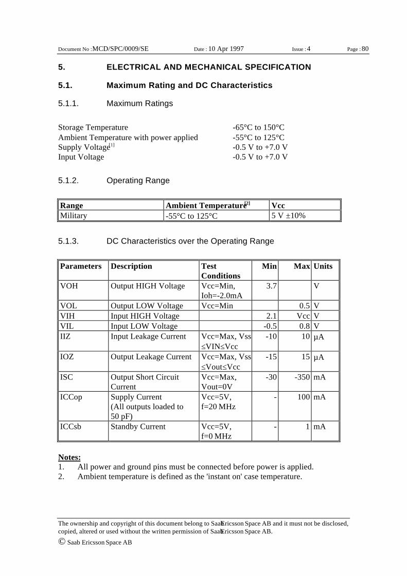
Page : 80
The ownership and copyright of this document belong to Saab Ericsson Space AB and it must not be disclosed,copied, altered or used without the written permission of Saab Ericsson Space AB.
© Saab Ericsson Space AB
Document No : MCD/SPC/0009/SE Date : 10 Apr 1997 Issue : 4
5. ELECTRICAL AND MECHANICAL SPECIFICATION
5.1. Maximum Rating and DC Characteristics
5.1.1. Maximum Ratings
Storage Temperature -65°C to 150°CAmbient Temperature with power applied -55°C to 125°CSupply Voltage[1] -0.5 V to +7.0 VInput Voltage -0.5 V to +7.0 V
5.1.2. Operating Range
Range Ambient Temperature[2] VccMilitary -55°C to 125°C 5 V ±10%
5.1.3. DC Characteristics over the Operating Range
Parameters Description TestConditions
Min Max Units
VOH Output HIGH Voltage Vcc=Min,Ioh=-2.0mA
3.7 V
VOL Output LOW Voltage Vcc=Min 0.5 VVIH Input HIGH Voltage 2.1 Vcc VVIL Input LOW Voltage -0.5 0.8 VIIZ Input Leakage Current Vcc=Max, Vss
≤VIN≤Vcc-10 10 µA
IOZ Output Leakage Current Vcc=Max, Vss≤Vout≤Vcc
-15 15 µA
ISC Output Short CircuitCurrent
Vcc=Max,Vout=0V
-30 -350 mA
ICCop Supply Current(All outputs loaded to50 pF)
Vcc=5V,f=20 MHz
- 100 mA
ICCsb Standby Current Vcc=5V,f=0 MHz
- 1 mA
Notes:1. All power and ground pins must be connected before power is applied.2. Ambient temperature is defined as the 'instant on' case temperature.
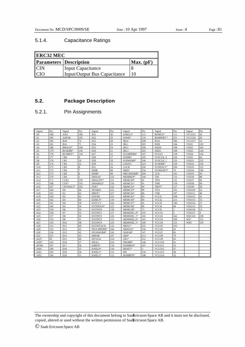
Page : 81
The ownership and copyright of this document belong to Saab Ericsson Space AB and it must not be disclosed,copied, altered or used without the written permission of Saab Ericsson Space AB.
© Saab Ericsson Space AB
Document No : MCD/SPC/0009/SE Date : 10 Apr 1997 Issue : 4
5.1.4. Capacitance Ratings
ERC32 MECParameters Description Max. (pF)CINCIO
Input CapacitanceInput/Output Bus Capacitance
810
5.2. Package Description
5.2.1. Pin Assignments
Signal Pin Signal Pin Signal Pin Signal Pin Signal Pin Signal PinA0 189 ASI3 190 D21 30 IOSEL3* 113 ROMCS* 111 VCCO15 26A1 185 ASPAR 195 D22 29 IOWR* 119 ROMWRT * 251 VCCO16 20A2 182 BA0 76 D23 28 IRL0 208 RXA 186 VCCO17 14A3 181 BA1 71 D24 23 IRL1 205 RXB 184 VSSI1 192A4 180 BHOLD* 148 D25 24 IRL2 206 SIZE0 199 VSSI2 163A5 179 BUSERR* 130 D26 21 IRL3 203 SIZE1 198 VSSI3 144A6 178 BUSRDY* 134 D27 22 IUCMPERR* 247 SYSAV 138 VSSI4 136A7 177 CB0 9 D28 17 IUERR* 245 SYSCLK_0 236 VSSI5 64A8 176 CB1 10 D29 18 IUHWERR* 246 SYSCLK_1 235 VSSO1 252A9 174 CB2 12 D30 15 LDSTO 223 SYSERR* 129 VSSO2 210A10 175 CB3 8 D31 16 LOCK 220 SYSHALT* 250 VSSO3 122A11 172 CB4 7 DDIR 99 MDS* 254 SYSRESET* 70 VSSO4 106A12 173 CB5 6 DDIR* 98 MECHWERR* 200 TCK 141 VSSO5 94A13 170 CB6 5 DMAAS 232 MEMBEN* 104 TDI 133 VSSO6 88A14 171 CLK2 239 DMAGNT* 231 MEMCS0* 92 TDO 131 VSSO7 82A15 168 COE* 143 DMAREQ* 228 MEMCS1* 91 TMS 139 VSSO8 69A16 167 CPUHALT* 202 DOE* 142 MEMCS2* 90 TRST* 137 VSSO9 58A17 166 D0 66 DPARIO 253 MEMCS3* 89 TXA 191 VSSO10 52A18 165 D1 62 DRDY* 227 MEMCS4* 86 TXB 187 VSSO11 46A19 164 D2 63 DXFER 222 MEMCS5* 83 VCCI1 248 VSSO12 41A20 162 D3 60 EXMCS* 110 MEMCS6* 84 VCCI2 211 VSSO13 33A21 161 D4 59 EXTCCV 226 MEMCS7* 81 VCCI3 140 VSSO14 27A22 160 D5 56 EXTHOLD* 225 MEMCS8* 80 VCCI4 68 VSSO15 19A23 159 D6 54 EXTINT0 128 MEMCS9* 75 VCCI5 1 VSSO16 13A24 158 D7 55 EXTINT1 127 MEMWR1_0* 103 VCCO1 2 VSSO17 4A25 157 D8 50 EXTINT2 126 MEMWR1_1* 102 VCCO2 242 WDCLK 238A26 155 D9 51 EXTINT3 125 MEMWR2_0* 101 VCCO3 209 WE* 215A27 154 D10 48 EXTINT4 124 MEMWR2_1* 100 VCCO4 121 WRT 219A28 153 D11 49 EXTINTACK 132 MEXC* 255 VCCO5 105A29 152 D12 45 FPUCMPERR* 244 MHOLD* 256 VCCO6 93A30 150 D13 42 FPUHWERR* 243 NOPAR* 147 VCCO7 85A31 151 D14 43 IMPAR 237 OE0* 213 VCCO8 79ALE* 95 D15 40 INTACK 214 OE1* 212 VCCO9 65AOE* 145 D16 37 INULL 224 PROM8* 146 VCCO10 61APAR 197 D17 36 IOBEN* 118 RAMBEN* 107 VCCO11 53ASI0 196 D18 35 IOSEL0* 116 RESET* 3 VCCO12 47ASI1 193 D19 34 IOSEL1* 115 RD 216 VCCO13 38ASI2 194 D20 31 IOSEL2* 112 ROMBEN* 108 VCCO14 32
Page : 82
The ownership and copyright of this document belong to Saab Ericsson Space AB and it must not be disclosed,copied, altered or used without the written permission of Saab Ericsson Space AB.
© Saab Ericsson Space AB
Document No : MCD/SPC/0009/SE Date : 10 Apr 1997 Issue : 4
5.2.2. Package Diagram
Page : 150/5050
The ownership and copyright of this document belong to Saab Ericsson Space AB and it must not be disclosed, copied, altered or usedwithout the written permission of Saab Ericsson Space AB. Saab Ericsson Space AB
Document No : MCD/SPC/0009/SE, APPENDIX 1 Date : 10 Apr 1997 Issue : 4
APPENDIX 1TIMING DIAGRAMS
(SYSCLK @ 10 MHz)
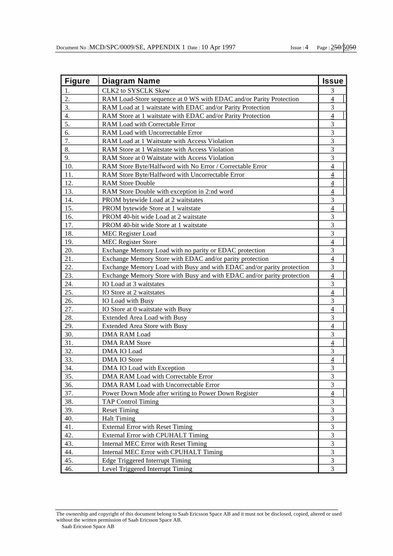
Page : 250/5050
The ownership and copyright of this document belong to Saab Ericsson Space AB and it must not be disclosed, copied, altered or usedwithout the written permission of Saab Ericsson Space AB. Saab Ericsson Space AB
Document No : MCD/SPC/0009/SE, APPENDIX 1 Date : 10 Apr 1997 Issue : 4
Figure Diagram Name Issue1. CLK2 to SYSCLK Skew 32. RAM Load-Store sequence at 0 WS with EDAC and/or Parity Protection 43. RAM Load at 1 waitstate with EDAC and/or Parity Protection 34. RAM Store at 1 waitstate with EDAC and/or Parity Protection 45. RAM Load with Correctable Error 36. RAM Load with Uncorrectable Error 37. RAM Load at 1 Waitstate with Access Violation 38. RAM Store at 1 Waitstate with Access Violation 39. RAM Store at 0 Waitstate with Access Violation 310. RAM Store Byte/Halfword with No Error / Correctable Error 411. RAM Store Byte/Halfword with Uncorrectable Error 412. RAM Store Double 413. RAM Store Double with exception in 2:nd word 414. PROM bytewide Load at 2 waitstates 315. PROM bytewide Store at 1 waitstate 416. PROM 40-bit wide Load at 2 waitstate 317. PROM 40-bit wide Store at 1 waitstate 318. MEC Register Load 319. MEC Register Store 420. Exchange Memory Load with no parity or EDAC protection 321. Exchange Memory Store with EDAC and/or parity protection 422. Exchange Memory Load with Busy and with EDAC and/or parity protection 323. Exchange Memory Store with Busy and with EDAC and/or parity protection 424. IO Load at 3 waitstates 325. IO Store at 2 waitstates 426. IO Load with Busy 327. IO Store at 0 waitstate with Busy 428. Extended Area Load with Busy 329. Extended Area Store with Busy 430. DMA RAM Load 331. DMA RAM Store 432. DMA IO Load 333. DMA IO Store 434. DMA IO Load with Exception 335. DMA RAM Load with Correctable Error 336. DMA RAM Load with Uncorrectable Error 337. Power Down Mode after writing to Power Down Register 438. TAP Control Timing 339. Reset Timing 340. Halt Timing 341. External Error with Reset Timing 342. External Error with CPUHALT Timing 343. Internal MEC Error with Reset Timing 344. Internal MEC Error with CPUHALT Timing 345. Edge Triggered Interrupt Timing 346. Level Triggered Interrupt Timing 3
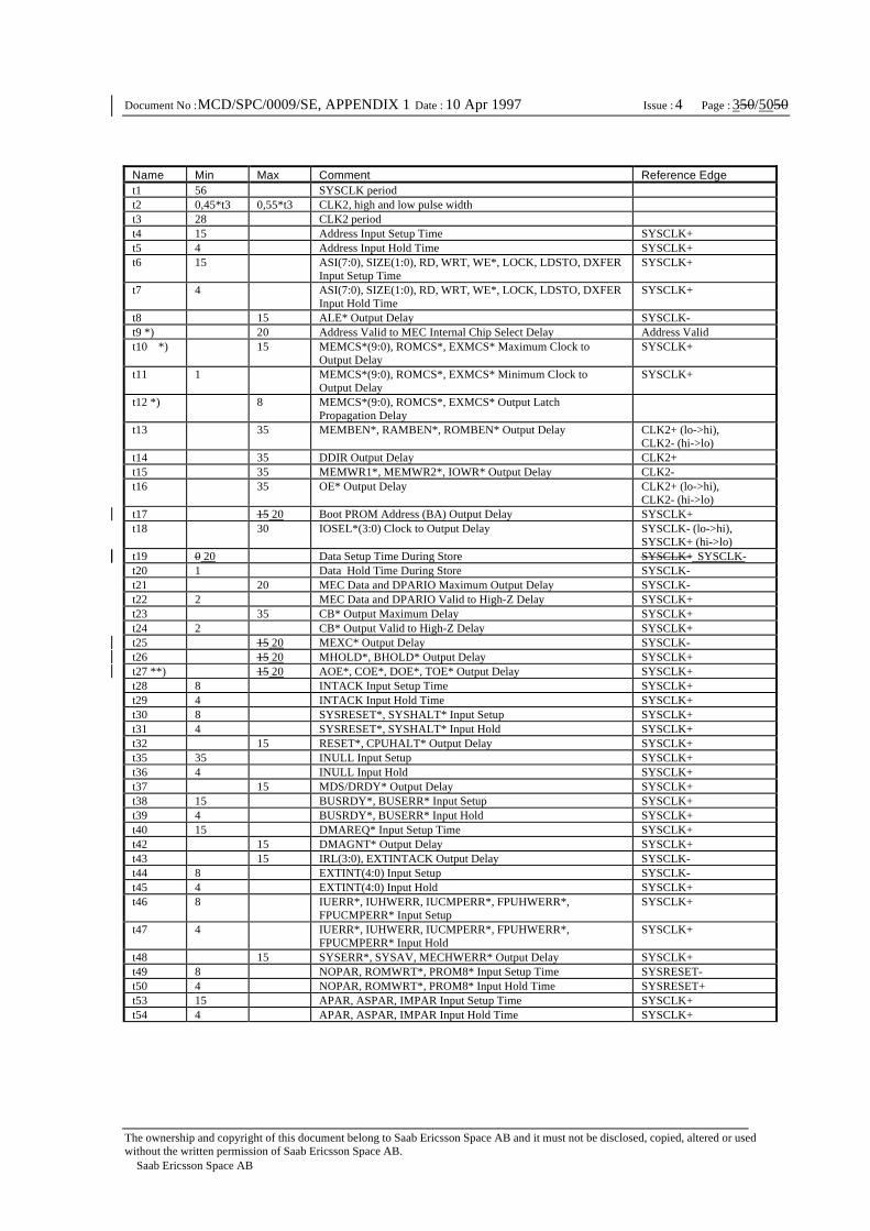
Page : 350/5050
The ownership and copyright of this document belong to Saab Ericsson Space AB and it must not be disclosed, copied, altered or usedwithout the written permission of Saab Ericsson Space AB. Saab Ericsson Space AB
Document No : MCD/SPC/0009/SE, APPENDIX 1 Date : 10 Apr 1997 Issue : 4
Name Min Max Comment Reference Edget1 56 SYSCLK periodt2 0,45*t3 0,55*t3 CLK2, high and low pulse widtht3 28 CLK2 periodt4 15 Address Input Setup Time SYSCLK+t5 4 Address Input Hold Time SYSCLK+t6 15 ASI(7:0), SIZE(1:0), RD, WRT, WE*, LOCK, LDSTO, DXFER
Input Setup TimeSYSCLK+
t7 4 ASI(7:0), SIZE(1:0), RD, WRT, WE*, LOCK, LDSTO, DXFERInput Hold Time
SYSCLK+
t8 15 ALE* Output Delay SYSCLK-t9 *) 20 Address Valid to MEC Internal Chip Select Delay Address Validt10 *) 15 MEMCS*(9:0), ROMCS*, EXMCS* Maximum Clock to
Output DelaySYSCLK+
t11 1 MEMCS*(9:0), ROMCS*, EXMCS* Minimum Clock toOutput Delay
SYSCLK+
t12 *) 8 MEMCS*(9:0), ROMCS*, EXMCS* Output LatchPropagation Delay
t13 35 MEMBEN*, RAMBEN*, ROMBEN* Output Delay CLK2+ (lo->hi),CLK2- (hi->lo)
t14 35 DDIR Output Delay CLK2+t15 35 MEMWR1*, MEMWR2*, IOWR* Output Delay CLK2-t16 35 OE* Output Delay CLK2+ (lo->hi),
CLK2- (hi->lo)t17 15 20 Boot PROM Address (BA) Output Delay SYSCLK+t18 30 IOSEL*(3:0) Clock to Output Delay SYSCLK- (lo->hi),
SYSCLK+ (hi->lo)t19 0 20 Data Setup Time During Store SYSCLK+ SYSCLK-t20 1 Data Hold Time During Store SYSCLK-t21 20 MEC Data and DPARIO Maximum Output Delay SYSCLK-t22 2 MEC Data and DPARIO Valid to High-Z Delay SYSCLK+t23 35 CB* Output Maximum Delay SYSCLK+t24 2 CB* Output Valid to High-Z Delay SYSCLK+t25 15 20 MEXC* Output Delay SYSCLK-t26 15 20 MHOLD*, BHOLD* Output Delay SYSCLK+t27 **) 15 20 AOE*, COE*, DOE*, TOE* Output Delay SYSCLK+t28 8 INTACK Input Setup Time SYSCLK+t29 4 INTACK Input Hold Time SYSCLK+t30 8 SYSRESET*, SYSHALT* Input Setup SYSCLK+t31 4 SYSRESET*, SYSHALT* Input Hold SYSCLK+t32 15 RESET*, CPUHALT* Output Delay SYSCLK+t35 35 INULL Input Setup SYSCLK+t36 4 INULL Input Hold SYSCLK+t37 15 MDS/DRDY* Output Delay SYSCLK+t38 15 BUSRDY*, BUSERR* Input Setup SYSCLK+t39 4 BUSRDY*, BUSERR* Input Hold SYSCLK+t40 15 DMAREQ* Input Setup Time SYSCLK+t42 15 DMAGNT* Output Delay SYSCLK+t43 15 IRL(3:0), EXTINTACK Output Delay SYSCLK-t44 8 EXTINT(4:0) Input Setup SYSCLK-t45 4 EXTINT(4:0) Input Hold SYSCLK+t46 8 IUERR*, IUHWERR, IUCMPERR*, FPUHWERR*,
FPUCMPERR* Input SetupSYSCLK+
t47 4 IUERR*, IUHWERR, IUCMPERR*, FPUHWERR*,FPUCMPERR* Input Hold
SYSCLK+
t48 15 SYSERR*, SYSAV, MECHWERR* Output Delay SYSCLK+t49 8 NOPAR, ROMWRT*, PROM8* Input Setup Time SYSRESET-t50 4 NOPAR, ROMWRT*, PROM8* Input Hold Time SYSRESET+t53 15 APAR, ASPAR, IMPAR Input Setup Time SYSCLK+t54 4 APAR, ASPAR, IMPAR Input Hold Time SYSCLK+
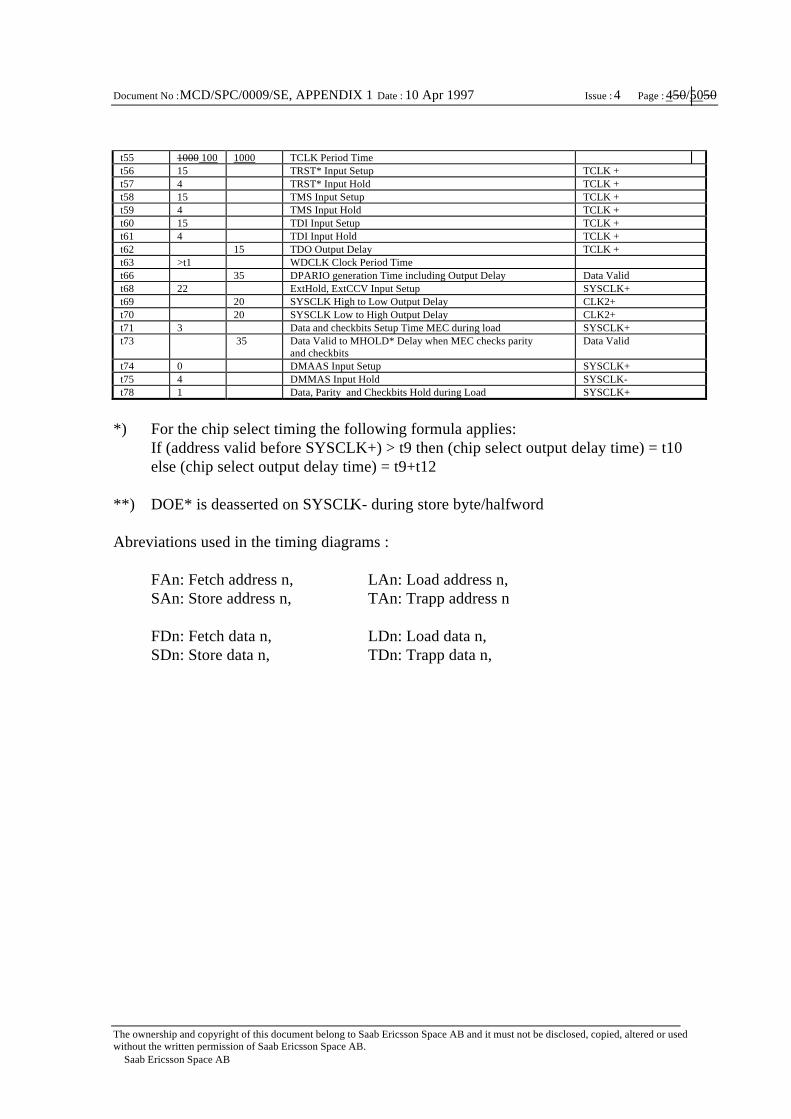
Page : 450/5050
The ownership and copyright of this document belong to Saab Ericsson Space AB and it must not be disclosed, copied, altered or usedwithout the written permission of Saab Ericsson Space AB. Saab Ericsson Space AB
Document No : MCD/SPC/0009/SE, APPENDIX 1 Date : 10 Apr 1997 Issue : 4
t55 1000 100 1000 TCLK Period Timet56 15 TRST* Input Setup TCLK +t57 4 TRST* Input Hold TCLK +t58 15 TMS Input Setup TCLK +t59 4 TMS Input Hold TCLK +t60 15 TDI Input Setup TCLK +t61 4 TDI Input Hold TCLK +t62 15 TDO Output Delay TCLK +t63 >t1 WDCLK Clock Period Timet66 35 DPARIO generation Time including Output Delay Data Validt68 22 ExtHold, ExtCCV Input Setup SYSCLK+t69 20 SYSCLK High to Low Output Delay CLK2+t70 20 SYSCLK Low to High Output Delay CLK2+t71 3 Data and checkbits Setup Time MEC during load SYSCLK+t73 35 Data Valid to MHOLD* Delay when MEC checks parity
and checkbitsData Valid
t74 0 DMAAS Input Setup SYSCLK+t75 4 DMMAS Input Hold SYSCLK-t78 1 Data, Parity and Checkbits Hold during Load SYSCLK+
*) For the chip select timing the following formula applies:If (address valid before SYSCLK+) > t9 then (chip select output delay time) = t10else (chip select output delay time) = t9+t12
**) DOE* is deasserted on SYSCLK- during store byte/halfword
Abreviations used in the timing diagrams :
FAn: Fetch address n, LAn: Load address n,SAn: Store address n, TAn: Trapp address n
FDn: Fetch data n, LDn: Load data n,SDn: Store data n, TDn: Trapp data n,
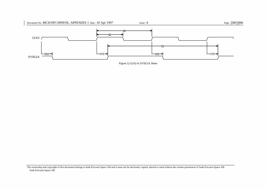
Page : 550/5050
The ownership and copyright of this document belong to Saab Ericsson Space AB and it must not be disclosed, copied, altered or used without the written permission of Saab Ericsson Space AB. Saab Ericsson Space AB
Document No : MCD/SPC/0009/SE, APPENDIX 1 Date : 10 Apr 1997 Issue : 4
t2t3
t2t3
t1t1
t69 t70 t69 t70
Figure 1) CLK2 to SYSCLK Skew
CLK2
SYSCLK
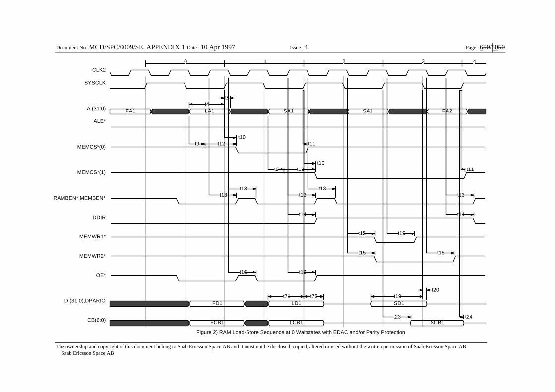
Page : 650/5050
The ownership and copyright of this document belong to Saab Ericsson Space AB and it must not be disclosed, copied, altered or used without the written permission of Saab Ericsson Space AB. Saab Ericsson Space AB
Document No : MCD/SPC/0009/SE, APPENDIX 1 Date : 10 Apr 1997 Issue : 4
0 1 2 3 4
t4t5
t71 t78 t19t20
t9 t12t10
t11
t9 t12t10
t11
t13t13
t13t13
t13
t14 t14
t15 t15
t15 t15
t16 t16
t23 t24
LA1
LCB1
SA1
SD1
SCB1
SA1
LD1
Figure 2) RAM Load-Store Sequence at 0 Waitstates with EDAC and/or Parity Protection
FA2
FD1
FCB1
FA1
CLK2
SYSCLK
A (31:0)
ALE*
MEMCS*(0)
MEMCS*(1)
RAMBEN*,MEMBEN*
DDIR
MEMWR1*
MEMWR2*
OE*
D (31:0),DPARIO
CB(6:0)
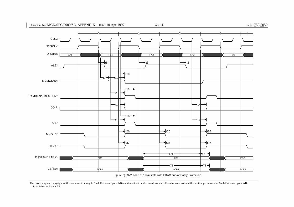
Page : 750/5050
The ownership and copyright of this document belong to Saab Ericsson Space AB and it must not be disclosed, copied, altered or used without the written permission of Saab Ericsson Space AB. Saab Ericsson Space AB
Document No : MCD/SPC/0009/SE, APPENDIX 1 Date : 10 Apr 1997 Issue : 4
0 1 2 3 4
t71 t78
t71 t78
t8 t8 t8
t9 t12t10
t13t13
t14 t14
t16t16
t16
t26 t26 t26
t37 t37 t37
LA1 FA2 FA2 FA3
LD1
Figure 3) RAM Load at 1 waitstate with EDAC and/or Parity Protection
LA1
FD1 FD2
LCB1FCB1 FCB2
CLK2
SYSCLK
A (31:0)
ALE*
MEMCS*(0)
RAMBEN*, MEMBEN*
DDIR
OE*
MHOLD*
MDS*
D (31:0),DPARIO
CB(6:0)
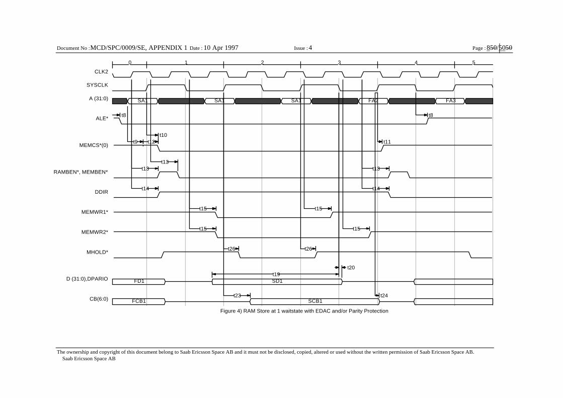
Page : 850/5050
The ownership and copyright of this document belong to Saab Ericsson Space AB and it must not be disclosed, copied, altered or used without the written permission of Saab Ericsson Space AB. Saab Ericsson Space AB
Document No : MCD/SPC/0009/SE, APPENDIX 1 Date : 10 Apr 1997 Issue : 4
0 1 2 3 4 5
t19t20
t8 t8
t9 t12t10
t11
t13t13
t13
t14 t14
t15 t15
t15 t15
t26 t26
t23 t24
SA1 SA1SA1 FA2
SCB1
SD1
Figure 4) RAM Store at 1 waitstate with EDAC and/or Parity Protection
FA3
FD1
FCB1
CLK2
SYSCLK
A (31:0)
ALE*
MEMCS*(0)
RAMBEN*, MEMBEN*
DDIR
MEMWR1*
MEMWR2*
MHOLD*
D (31:0),DPARIO
CB(6:0)
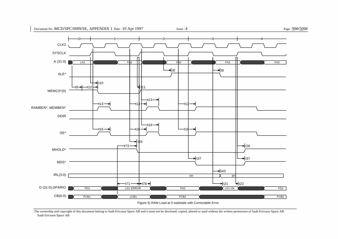
Page : 950/5050
The ownership and copyright of this document belong to Saab Ericsson Space AB and it must not be disclosed, copied, altered or used without the written permission of Saab Ericsson Space AB. Saab Ericsson Space AB
Document No : MCD/SPC/0009/SE, APPENDIX 1 Date : 10 Apr 1997 Issue : 4
0 1 2 3 4
t71 t78
t8 t8
t9 t12t10
t11
t13 t13t13
t13
t16 t16t16
t16
t26t73 t26
t37 t37
t43
t21 t22
LA1 FA2 FA2
LD1 ERROR
0H 6H
FA2
LD1 OK
Figure 5) RAM Load at 0 waitstate with Correctable Error
FA3
LCB1
FD1
FCB1
FD2
FCB2
FD2
FCB2
CLK2
SYSCLK
A (31:0)
ALE*
MEMCS*(0)
RAMBEN*, MEMBEN*
DDIR
OE*
MHOLD*
MDS*
IRL(3:0)
D (31:0),DPARIO
CB(6:0)
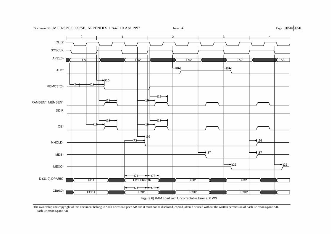
Page : 1050/5050
The ownership and copyright of this document belong to Saab Ericsson Space AB and it must not be disclosed, copied, altered or used without the written permission of Saab Ericsson Space AB. Saab Ericsson Space AB
Document No : MCD/SPC/0009/SE, APPENDIX 1 Date : 10 Apr 1997 Issue : 4
0 1 2 3 4
t71 t78
t71 t78
t8 t8
t9 t12t10
t13 t13t13
t16t16
t16t16
t73t26
t26
t37 t37
t25 t25
LA1 FA2 FA2
LD1 ERROR
FA2
FD2
Figure 6) RAM Load with Uncorrectable Error at 0 WS
FA3
LCB1
FD2
FCB2
FD1
FCB1 FCB2
CLK2
SYSCLK
A (31:0)
ALE*
MEMCS*(0)
RAMBEN*, MEMBEN*
DDIR
OE*
MHOLD*
MDS*
MEXC*
D (31:0),DPARIO
CB(6:0)
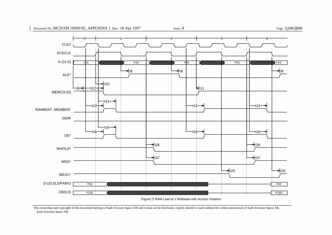
Page : 1150/5050
The ownership and copyright of this document belong to Saab Ericsson Space AB and it must not be disclosed, copied, altered or used without the written permission of Saab Ericsson Space AB. Saab Ericsson Space AB
Document No : MCD/SPC/0009/SE, APPENDIX 1 Date : 10 Apr 1997 Issue : 4
0 1 2 3 4
t8 t8 t8
t9 t12t10
t11
t13t13
t13 t13
t16t16
t16 t16
t26 t26
t37 t37
t25 t25
Figure 7) RAM Load at 1 Waitstate with Access Violation
LA1 FA2 FA2 FA2 FA3
FD1
FCB1
FD2
FCB2
CLK2
SYSCLK
A (31:0)
ALE*
MEMCS*(0)
RAMBEN*, MEMBEN*
DDIR
OE*
MHOLD*
MDS*
MEXC*
D (31:0),DPARIO
CB(6:0)
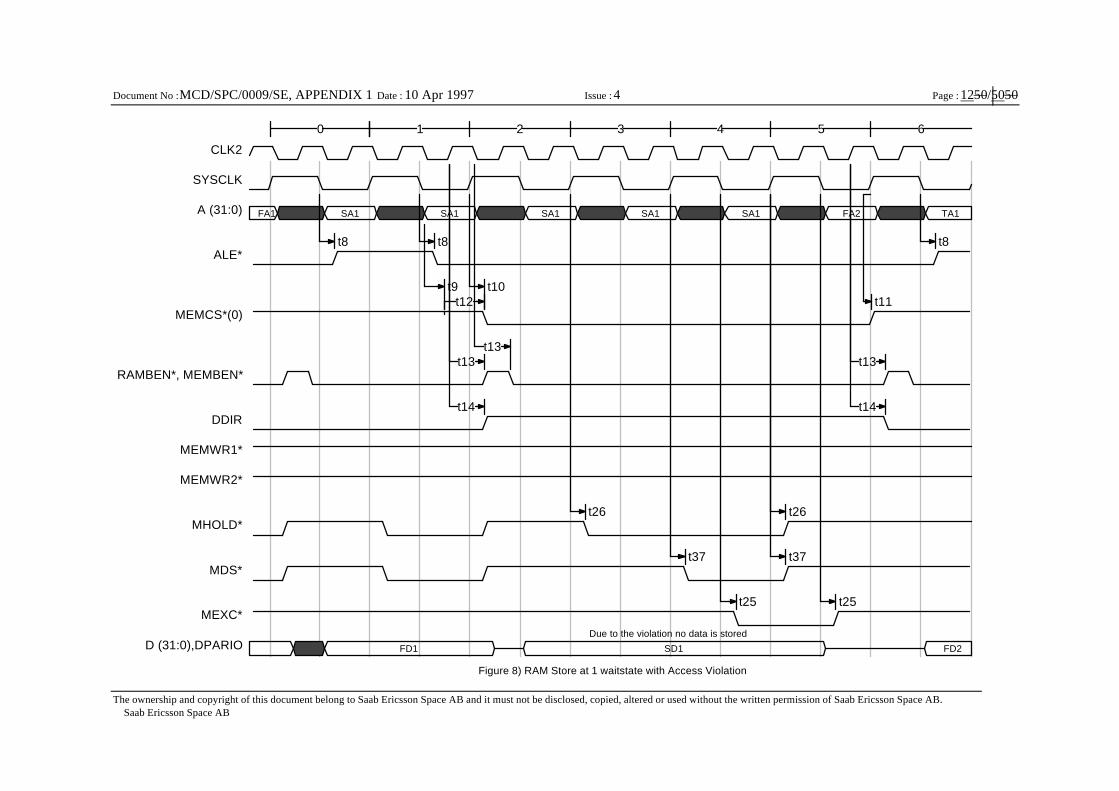
Page : 1250/5050
The ownership and copyright of this document belong to Saab Ericsson Space AB and it must not be disclosed, copied, altered or used without the written permission of Saab Ericsson Space AB. Saab Ericsson Space AB
Document No : MCD/SPC/0009/SE, APPENDIX 1 Date : 10 Apr 1997 Issue : 4
0 1 2 3 4 5 6
t8 t8 t8
t9t12
t10t11
t13t13
t13
t14 t14
t26 t26
t37 t37
t25 t25
SA1 SA1SA1 SA1
Due to the violation no data is stored
Figure 8) RAM Store at 1 waitstate with Access Violation
SA1FA1 FA2 TA1
SD1FD1 FD2
CLK2
SYSCLK
A (31:0)
ALE*
MEMCS*(0)
RAMBEN*, MEMBEN*
DDIR
MEMWR1*
MEMWR2*
MHOLD*
MDS*
MEXC*
D (31:0),DPARIO
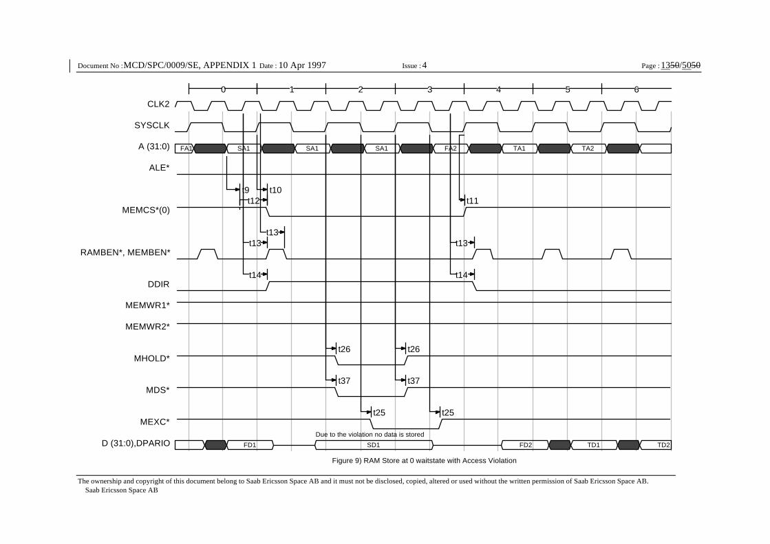
Page : 1350/5050
The ownership and copyright of this document belong to Saab Ericsson Space AB and it must not be disclosed, copied, altered or used without the written permission of Saab Ericsson Space AB. Saab Ericsson Space AB
Document No : MCD/SPC/0009/SE, APPENDIX 1 Date : 10 Apr 1997 Issue : 4
0 1 2 3 4 5 6
t9t12
t10t11
t13t13
t13
t14 t14
t26 t26
t37 t37
t25 t25
SA1 FA2SA1 TA1
Due to the violation no data is stored
Figure 9) RAM Store at 0 waitstate with Access Violation
SA1FA1
SD1FD1
TA2
FD2 TD1 TD2
CLK2
SYSCLK
A (31:0)
ALE*
MEMCS*(0)
RAMBEN*, MEMBEN*
DDIR
MEMWR1*
MEMWR2*
MHOLD*
MDS*
MEXC*
D (31:0),DPARIO
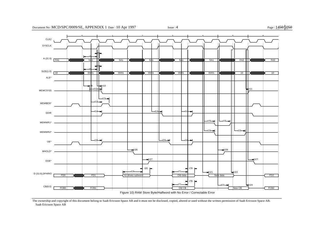
Page : 1450/5050
The ownership and copyright of this document belong to Saab Ericsson Space AB and it must not be disclosed, copied, altered or used without the written permission of Saab Ericsson Space AB. Saab Ericsson Space AB
Document No : MCD/SPC/0009/SE, APPENDIX 1 Date : 10 Apr 1997 Issue : 4
0 1 2 3 4 5 6
t4t5
t6t7
t19t20
t71t78
t71t78
t9t12
t10t11
t13t13
t14 t14 t14
t15 t15
t15 t15
t16 t16 t16
t26 t26
t27 t27
t21 t22
t23 t24
SA1 SA1SA1 SA1
IU drives subword
New CB
SA1 FA2
00/01 00/01 00/01 00/01 00/01 10
Old data New data
Figure 10) RAM Store Byte/Halfword with No Error / Correctable Error
10
FA1
10
FA3
Old CB
FD1FD0
FCB0 FCB1
FD2
FCB2
CLK2
SYSCLK
A (31:0)
SIZE(1:0)
ALE*
MEMCS*(0)
MEMBEN*
DDIR
MEMWR1*
MEMWR2*
OE*
MHOLD*
DOE*
D (31:0),DPARIO
CB(6:0)
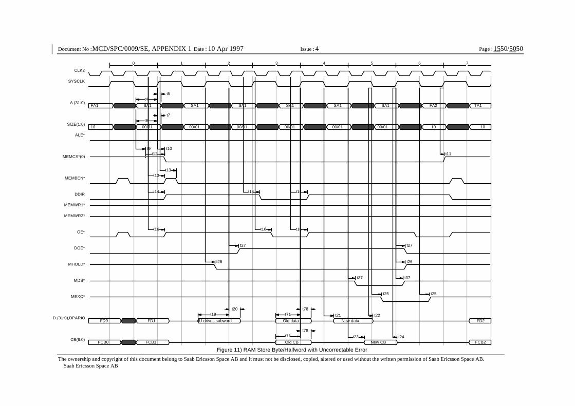
Page : 1550/5050
The ownership and copyright of this document belong to Saab Ericsson Space AB and it must not be disclosed, copied, altered or used without the written permission of Saab Ericsson Space AB. Saab Ericsson Space AB
Document No : MCD/SPC/0009/SE, APPENDIX 1 Date : 10 Apr 1997 Issue : 4
0 1 2 3 4 5 6 7
t4t5
t6t7
t19t20
t71t78
t71t78
t9t12
t10t11
t13t13
t14 t14 t14
t16 t16 t16
t27 t27
t26 t26
t37 t37
t25 t25
t21 t22
t23 t24
SA1 SA1SA1 SA1
IU drives subword
New CB
SA1 SA1
00/01 00/01 00/01 00/01 00/01 00/01
Old data New data
Figure 11) RAM Store Byte/Halfword with Uncorrectable Error
10
FA1
10
TA1
Old CB
FD1FD0
FCB0 FCB1
FD2
FCB2
FA2
10
CLK2
SYSCLK
A (31:0)
SIZE(1:0)
ALE*
MEMCS*(0)
MEMBEN*
DDIR
MEMWR1*
MEMWR2*
OE*
DOE*
MHOLD*
MDS*
MEXC*
D (31:0),DPARIO
CB(6:0)
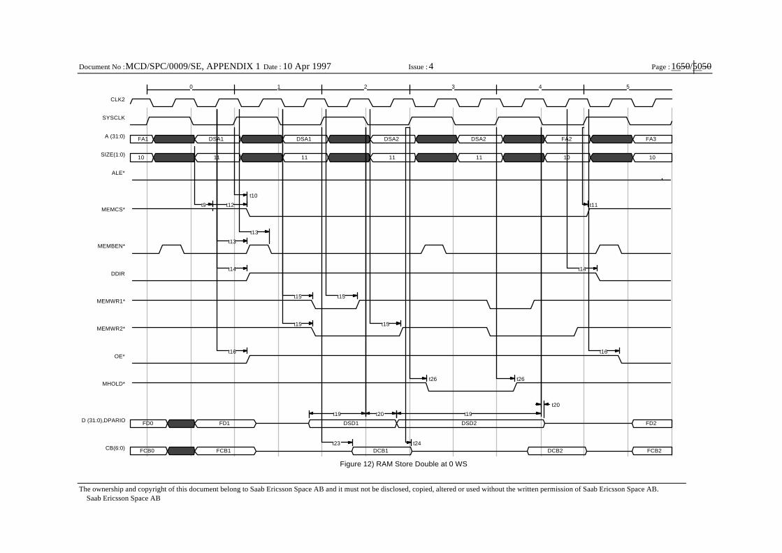
Page : 1650/5050
The ownership and copyright of this document belong to Saab Ericsson Space AB and it must not be disclosed, copied, altered or used without the written permission of Saab Ericsson Space AB. Saab Ericsson Space AB
Document No : MCD/SPC/0009/SE, APPENDIX 1 Date : 10 Apr 1997 Issue : 4
0 1 2 3 4 5
t19 t19t20
t20
t9 t12
t10
t11
t13
t13
t14 t14
t15 t15
t15 t15
t16 t16
t26 t26
t23 t24
DSA1 DSA2DSA1 DSA2
FD1 DSD1
DCB1
FA2
DSD2
11 11 11 11 10
DCB2
Figure 12) RAM Store Double at 0 WS
FA1
10
FCB1
FD0
FCB0
FD2
FCB2
FA3
10
CLK2
SYSCLK
A (31:0)
SIZE(1:0)
ALE*
MEMCS*
MEMBEN*
DDIR
MEMWR1*
MEMWR2*
OE*
MHOLD*
D (31:0),DPARIO
CB(6:0)
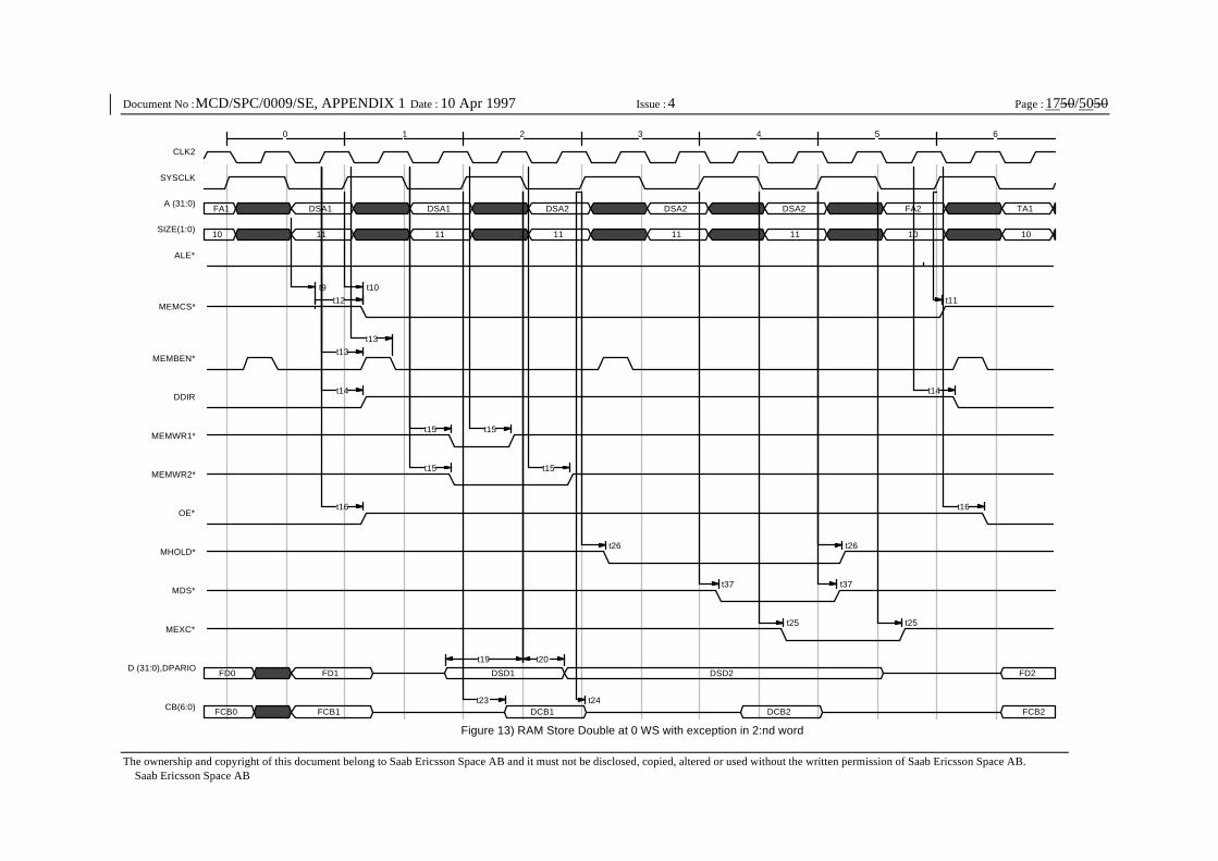
Page : 1750/5050
The ownership and copyright of this document belong to Saab Ericsson Space AB and it must not be disclosed, copied, altered or used without the written permission of Saab Ericsson Space AB. Saab Ericsson Space AB
Document No : MCD/SPC/0009/SE, APPENDIX 1 Date : 10 Apr 1997 Issue : 4
0 1 2 3 4 5 6
t19 t20
t9t12
t10t11
t13t13
t14 t14
t15 t15
t15 t15
t16 t16
t26 t26
t37 t37
t25 t25
t23 t24
DSA1 DSA2DSA1 DSA2
FD1 DSD1
DCB1
DSA2
DSD2
11 11 11 11 11
DCB2
Figure 13) RAM Store Double at 0 WS with exception in 2:nd word
FA1
10
FCB1
FD0
FCB0
FD2
FCB2
FA2 TA1
10 10
CLK2
SYSCLK
A (31:0)
SIZE(1:0)
ALE*
MEMCS*
MEMBEN*
DDIR
MEMWR1*
MEMWR2*
OE*
MHOLD*
MDS*
MEXC*
D (31:0),DPARIO
CB(6:0)
Page : 1850/5050
The ownership and copyright of this document belong to Saab Ericsson Space AB and it must not be disclosed, copied, altered or used without the written permission of Saab Ericsson Space AB. Saab Ericsson Space AB
Document No : MCD/SPC/0009/SE, APPENDIX 1 Date : 10 Apr 1997 Issue : 4
0 1 2 3 4 5--7 8 9 10 11
ACCESS OF BYTE 2 AND 1 ARE NOT SHOWN HERE ACCESS OF BYTE 2 AND 1 ARE NOT SHOWN HERE
t71t78
t71t78
t8 t8
t12 t10t9 t11
t13 t13
t13t13
t13 t13
t16t16
t16
t17 t17 t17 t17
t26 t26
t37 t37
t21 t22
t21 t22
00 01/10
LD1 IU DATALD1 BYTE 3
generated
Figure 14) PROM bytewide Load at 2 waitstates
LD BYTE 0
FA1 LA1 FA2 FA2 FA2 FA2 FA2 FA2 FA2 FA2 FA3
00 11
BYTE 2/1FD1
FDP1
CLK2
SYSCLK
A (31:0)
ALE*
ROMCS*
ROMBEN*
MEMBEN*
DDIR
OE*
BA(1:0)
MHOLD*
MDS*
D (31:0)
DPARIO
Page : 1950/5050
The ownership and copyright of this document belong to Saab Ericsson Space AB and it must not be disclosed, copied, altered or used without the written permission of Saab Ericsson Space AB. Saab Ericsson Space AB
Document No : MCD/SPC/0009/SE, APPENDIX 1 Date : 10 Apr 1997 Issue : 4
0 1 2 3 4
t19t20
t8 t8
t10 t11
t13 t13t13
t13 t13
t13 t13
t14 t14
t15 t15
t16 t16
t17 t17
t26 t26
SA1
BYTE ADDRESS
00 10 10
SA1
Fig 15) PROM Bytewide Store at 1 WS
00 00
SA1 FA2 FA2
FD1 SD1 FD2
CLK2
SYSCLK
A (31:0)
SIZE(1:0)
ALE*
ROMCS*
MEMBEN*
ROMBEN*
RAMBEN*
DDIR
MEMWR1*
OE*
BA(1:0)
MHOLD*
D (7:0)
Page : 2050/5050
The ownership and copyright of this document belong to Saab Ericsson Space AB and it must not be disclosed, copied, altered or used without the written permission of Saab Ericsson Space AB. Saab Ericsson Space AB
Document No : MCD/SPC/0009/SE, APPENDIX 1 Date : 10 Apr 1997 Issue : 4
0 1 2 3 4 5
t71t78
t71t78
t8
t10 t11
t13 t13
t13 t13
t16 t16
t26 t26
t37 t37
PROMtpd
PROMtpd
LA1 FA2 FA2 FA3
LD1
LCB1
FD2
Fig 16) PROM 40 bit wide load at 2 WS
FA1 FA2
FD1
FCB1
FD0
FCB0 FCB2
CLK2
SYSCLK
A (31:0)
ALE*
ROMCS*
MEMBEN*
ROMBEN*
RAMBEN*
DDIR
OE*
MHOLD*
MDS*
D (31:0),DPARIO
CB(6:0)
Page : 2150/5050
The ownership and copyright of this document belong to Saab Ericsson Space AB and it must not be disclosed, copied, altered or used without the written permission of Saab Ericsson Space AB. Saab Ericsson Space AB
Document No : MCD/SPC/0009/SE, APPENDIX 1 Date : 10 Apr 1997 Issue : 4
0 1 2 3 4 5
t10 t11
t13 t13
t13 t13
t14 t14
t15 t15
t15 t15
t16 t16
t26 t26
IUDATAtpd IUDATAhold
t23 t20
SA1 SA1 FA2 FA3
LD1
LCB1
FD2
Fig 17) PROM 40 bit wide store at 1 WS
FA1 SA1
FD1
FCB1
FD0
FCB0 FCB2
CLK2
SYSCLK
A (31:0)
ALE*
ROMCS*
MEMBEN*
ROMBEN*
RAMBEN*
DDIR
MEMWR1*
MEMWR2*
OE*
MHOLD*
D (31:0),DPARIO
CB(6:0)
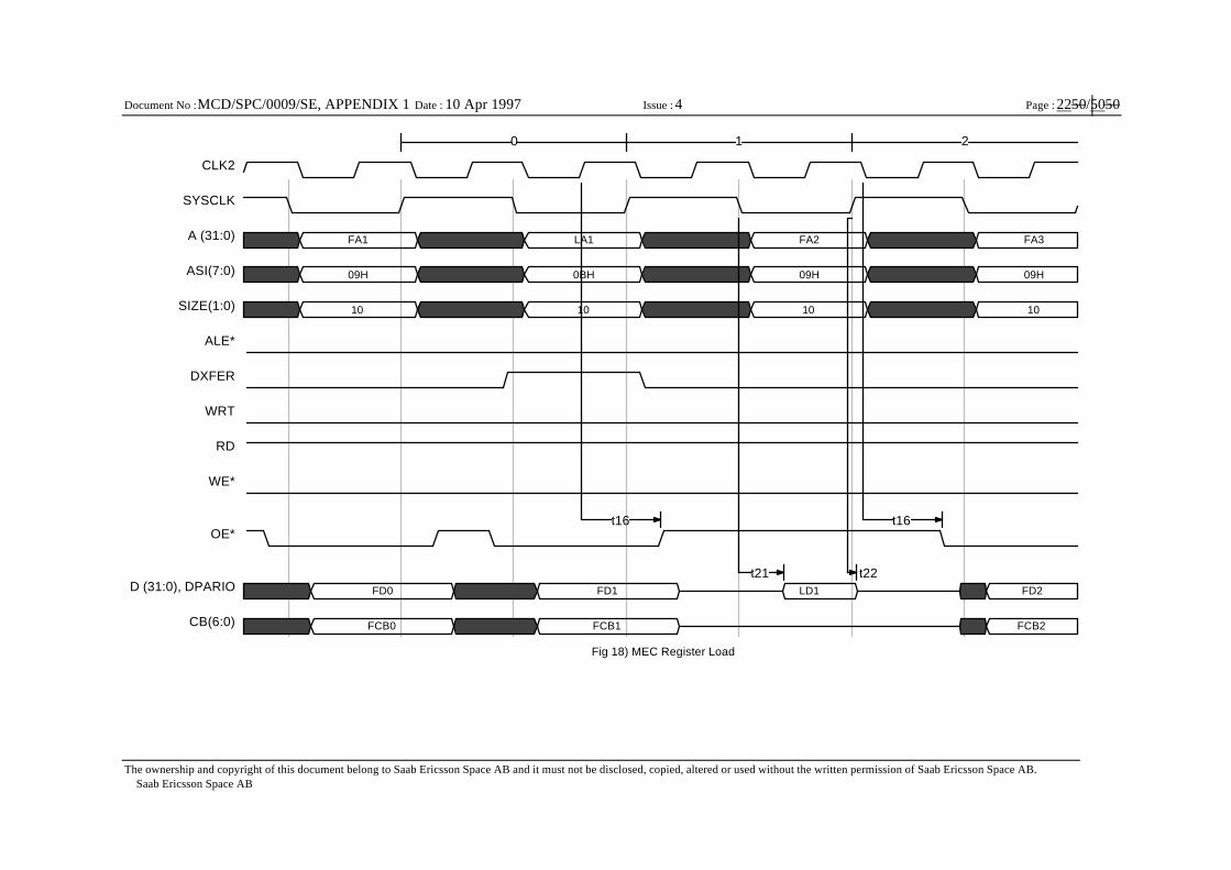
Page : 2250/5050
The ownership and copyright of this document belong to Saab Ericsson Space AB and it must not be disclosed, copied, altered or used without the written permission of Saab Ericsson Space AB. Saab Ericsson Space AB
Document No : MCD/SPC/0009/SE, APPENDIX 1 Date : 10 Apr 1997 Issue : 4
0 1 2
t16 t16
t21 t22
LA1 FA2 FA3
FD2
0BH 09H 09H
10 10 10
LD1
Fig 18) MEC Register Load
FA1
09H
10
FCB2
FD1FD0
FCB1FCB0
CLK2
SYSCLK
A (31:0)
ASI(7:0)
SIZE(1:0)
ALE*
DXFER
WRT
RD
WE*
OE*
D (31:0), DPARIO
CB(6:0)
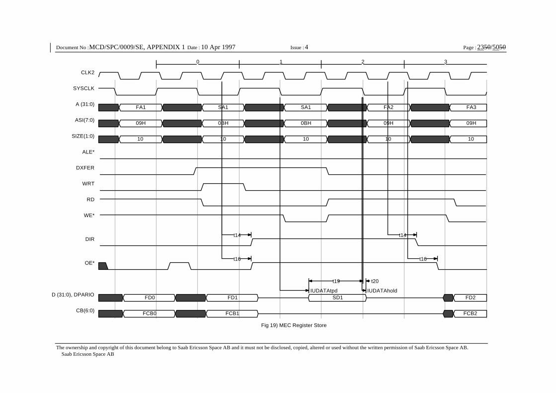
Page : 2350/5050
The ownership and copyright of this document belong to Saab Ericsson Space AB and it must not be disclosed, copied, altered or used without the written permission of Saab Ericsson Space AB. Saab Ericsson Space AB
Document No : MCD/SPC/0009/SE, APPENDIX 1 Date : 10 Apr 1997 Issue : 4
0 1 2 3
t19 t20
t14 t14
t16 t16
IUDATAtpd IUDATAhold
SA1 SA1 FA2
FD2
0BH 0BH 09H
10 10 10
SD1
Fig 19) MEC Register Store
FA1
09H
10
FCB2
FD1FD0
FCB1FCB0
FA3
09H
10
CLK2
SYSCLK
A (31:0)
ASI(7:0)
SIZE(1:0)
ALE*
DXFER
WRT
RD
WE*
DIR
OE*
D (31:0), DPARIO
CB(6:0)
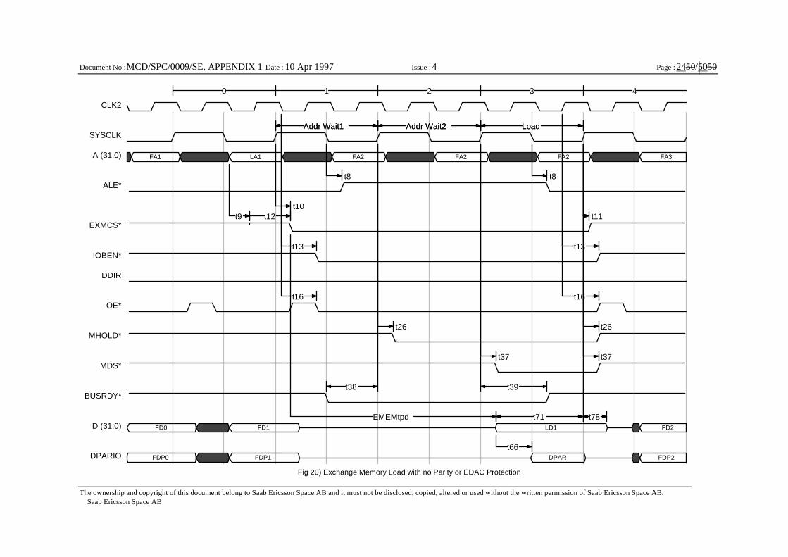
Page : 2450/5050
The ownership and copyright of this document belong to Saab Ericsson Space AB and it must not be disclosed, copied, altered or used without the written permission of Saab Ericsson Space AB. Saab Ericsson Space AB
Document No : MCD/SPC/0009/SE, APPENDIX 1 Date : 10 Apr 1997 Issue : 4
0 1 2 3 4
Addr Wait1Addr Wait1 Addr Wait2Addr Wait2 LoadLoad
t38 t39
t71 t78
t8 t8
t9 t12t10
t11
t13 t13
t16 t16
t26 t26
t37 t37
EMEMtpd
t66
LA1 FA2 FA2 FA2
LD1
FA3
DPAR
Fig 20) Exchange Memory Load with no Parity or EDAC Protection
FA1
FD0 FD1 FD2
FDP0 FDP1 FDP2
CLK2
SYSCLK
A (31:0)
ALE*
EXMCS*
IOBEN*
DDIR
OE*
MHOLD*
MDS*
BUSRDY*
D (31:0)
DPARIO

Page : 2550/5050
The ownership and copyright of this document belong to Saab Ericsson Space AB and it must not be disclosed, copied, altered or used without the written permission of Saab Ericsson Space AB. Saab Ericsson Space AB
Document No : MCD/SPC/0009/SE, APPENDIX 1 Date : 10 Apr 1997 Issue : 4
0 1 2 3 4 5
Addr Wait1Addr Wait1 Addr Wait2Addr Wait2 Store 1Store 1 Store 2Store 2
t38 t39
t19t20
t9 t12t10
t11
t13 t13
t14 t14
t15 t15
t15 t15
t16 t16
t26 t26
IUDATAtpd IUDATAhold
t23 t24
SA1 SA1 SA1 FA2
SD1
FA3
SCB1
Fig 21) Exchange Memory Store with EDAC and/or Parity Protection
FA1
FD0 FD1 FD2
FCB0 FCB1 FCB2
SA1
CLK2
SYSCLK
A (31:0)
ALE*
EXMCS*
IOBEN*
DDIR
IOWR*
MEMWR2*
OE*
MHOLD*
MDS*
BUSRDY*
D (31:0), DPARIO
CB(6:0)
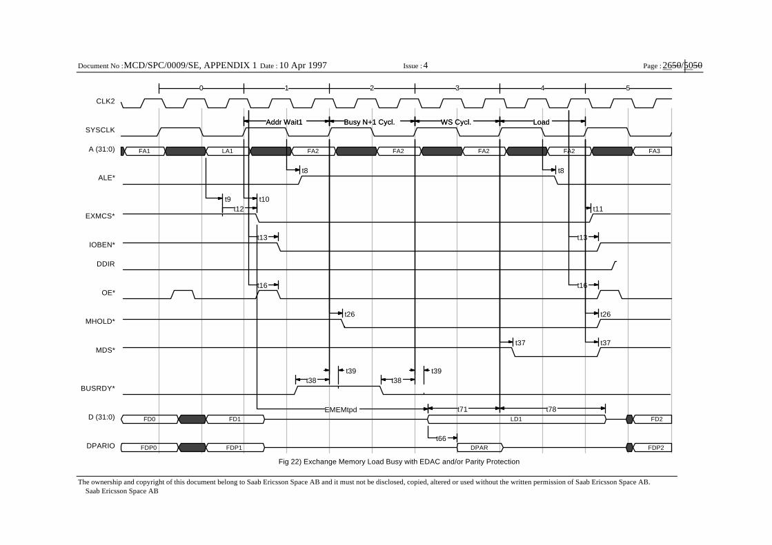
Page : 2650/5050
The ownership and copyright of this document belong to Saab Ericsson Space AB and it must not be disclosed, copied, altered or used without the written permission of Saab Ericsson Space AB. Saab Ericsson Space AB
Document No : MCD/SPC/0009/SE, APPENDIX 1 Date : 10 Apr 1997 Issue : 4
0 1 2 3 4 5
Addr Wait1Addr Wait1 Busy N+1 Cycl.Busy N+1 Cycl. WS Cycl. LoadWS Cycl. Load
t38t39
t38t39
t71 t78
t8 t8
t9t12
t10t11
t13 t13
t16 t16
t26 t26
t37 t37
EMEMtpd
t66
LA1 FA2 FA2 FA2
LD1
FA2
DPAR
Fig 22) Exchange Memory Load Busy with EDAC and/or Parity Protection
FA1
FD0 FD1 FD2
FDP0 FDP1 FDP2
FA3
CLK2
SYSCLK
A (31:0)
ALE*
EXMCS*
IOBEN*
DDIR
OE*
MHOLD*
MDS*
BUSRDY*
D (31:0)
DPARIO
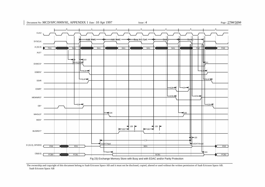
Page : 2750/5050
The ownership and copyright of this document belong to Saab Ericsson Space AB and it must not be disclosed, copied, altered or used without the written permission of Saab Ericsson Space AB. Saab Ericsson Space AB
Document No : MCD/SPC/0009/SE, APPENDIX 1 Date : 10 Apr 1997 Issue : 4
0 1 2 3 4 5 6
Addr Wait1Addr Wait1 Addr Wait2Addr Wait2 Busy N+1 Cycl. Store 1Busy N+1 Cycl. Store 1 Store 2Store 2
t38t39
t38t39
t19t20
t9t12
t10t11
t13 t13
t14 t14
t15 t15
t15 t15
t16 t16
t26 t26
IUDATAtpd IUDATAhold
t23 t24
SA1 SA1 SA1 FA2
SD1
FA3
SCB1
Fig 23) Exchange Memory Store with Busy and with EDAC and/or Parity Protection
FA1
FD0 FD1 FD2
FCB0 FCB1 FCB2
SA1 SA1
CLK2
SYSCLK
A (31:0)
ALE*
EXMCS*
IOBEN*
DDIR
IOWR*
MEMWR2*
OE*
MHOLD*
MDS*
BUSRDY*
D (31:0), DPARIO
CB(6:0)
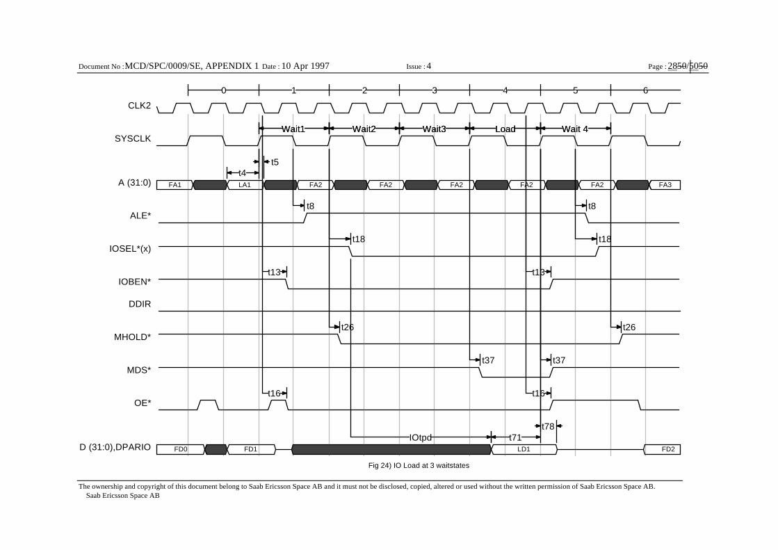
Page : 2850/5050
The ownership and copyright of this document belong to Saab Ericsson Space AB and it must not be disclosed, copied, altered or used without the written permission of Saab Ericsson Space AB. Saab Ericsson Space AB
Document No : MCD/SPC/0009/SE, APPENDIX 1 Date : 10 Apr 1997 Issue : 4
0 1 2 3 4 5 6
Wait1Wait1 Wait2Wait2 Wait3Wait3 Load Wait 4Load Wait 4
t4t5
t71t78
t8 t8
t18 t18
t13 t13
t26 t26
t37 t37
t16 t16
IOtpd
LA1 FA2 FA2 FA2FA2
LD1
FA2
Fig 24) IO Load at 3 waitstates
FA3FA1
FD1FD0 FD2
CLK2
SYSCLK
A (31:0)
ALE*
IOSEL*(x)
IOBEN*
DDIR
MHOLD*
MDS*
OE*
D (31:0),DPARIO
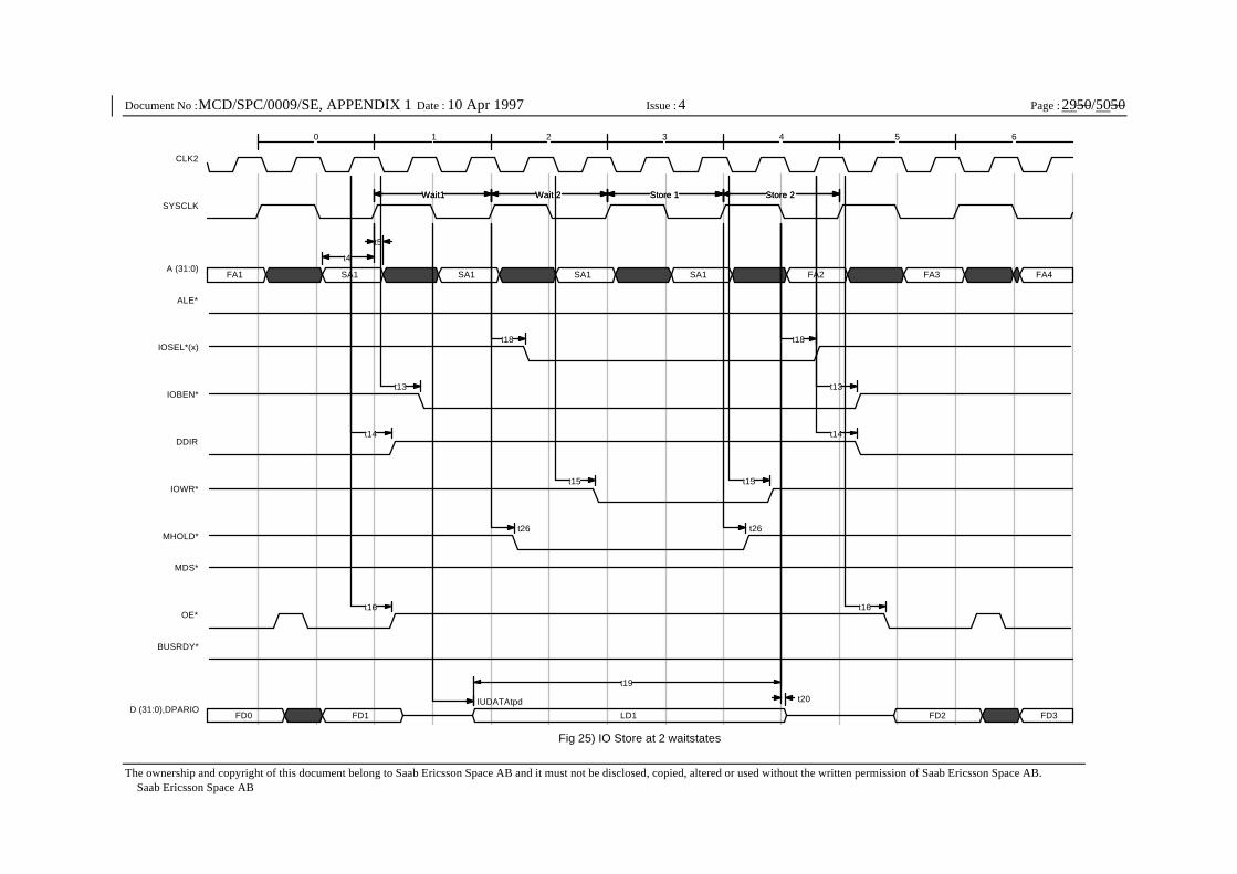
Page : 2950/5050
The ownership and copyright of this document belong to Saab Ericsson Space AB and it must not be disclosed, copied, altered or used without the written permission of Saab Ericsson Space AB. Saab Ericsson Space AB
Document No : MCD/SPC/0009/SE, APPENDIX 1 Date : 10 Apr 1997 Issue : 4
0 1 2 3 4 5 6
Wait1Wait1 Wait 2Wait 2 Store 1 Store 2Store 1 Store 2
t4
t5
t19
t20
t18 t18
t13 t13
t14 t14
t15 t15
t26 t26
t16 t16
IUDATAtpd
SA1 SA1 SA1 FA3FA2
LD1
SA1
Fig 25) IO Store at 2 waitstates
FA4FA1
FD1FD0 FD3FD2
CLK2
SYSCLK
A (31:0)
ALE*
IOSEL*(x)
IOBEN*
DDIR
IOWR*
MHOLD*
MDS*
OE*
BUSRDY*
D (31:0),DPARIO
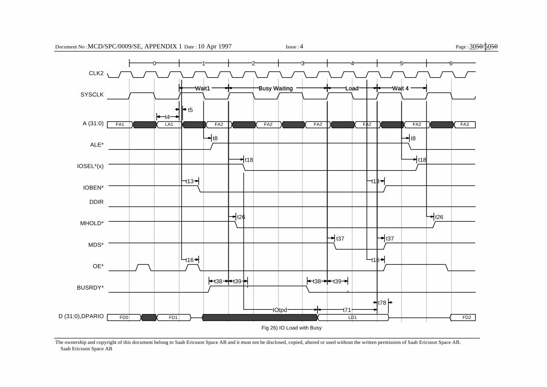
Page : 3050/5050
The ownership and copyright of this document belong to Saab Ericsson Space AB and it must not be disclosed, copied, altered or used without the written permission of Saab Ericsson Space AB. Saab Ericsson Space AB
Document No : MCD/SPC/0009/SE, APPENDIX 1 Date : 10 Apr 1997 Issue : 4
0 1 2 3 4 5 6
Wait1Wait1 Busy WaitingBusy Waiting Load Wait 4Load Wait 4
t4t5
t38 t39 t38 t39
t71t78
t8 t8
t18 t18
t13 t13
t26 t26
t37 t37
t16 t16
IOtpd
LA1 FA2 FA2 FA2FA2
LD1
FA2
Fig 26) IO Load with Busy
FA3FA1
FD1FD0 FD2
CLK2
SYSCLK
A (31:0)
ALE*
IOSEL*(x)
IOBEN*
DDIR
MHOLD*
MDS*
OE*
BUSRDY*
D (31:0),DPARIO
Page : 3150/5050
The ownership and copyright of this document belong to Saab Ericsson Space AB and it must not be disclosed, copied, altered or used without the written permission of Saab Ericsson Space AB. Saab Ericsson Space AB
Document No : MCD/SPC/0009/SE, APPENDIX 1 Date : 10 Apr 1997 Issue : 4
0 1 2 3 4 5 6
Wait1Wait1 Busy waitingBusy waiting Store 1 Store 2Store 1 Store 2
t4t5
t38 t39 t38 t39
t19t20
t18 t18
t13 t13
t14 t14
t15 t15
t26 t26
t16 t16
IUDATAtpd
SA1 SA1 SA1 FA3FA2
STD1
SA1
Fig 27) IO Store at 0 waitstates with Busy
FA4FA1
FD1FD0 FD3FD2
CLK2
SYSCLK
A (31:0)
ALE*
IOSEL*(x)
IOBEN*
DDIR
IOWR*
MHOLD*
MDS*
OE*
BUSRDY*
D (31:0),DPARIO
Page : 3250/5050
The ownership and copyright of this document belong to Saab Ericsson Space AB and it must not be disclosed, copied, altered or used without the written permission of Saab Ericsson Space AB. Saab Ericsson Space AB
Document No : MCD/SPC/0009/SE, APPENDIX 1 Date : 10 Apr 1997 Issue : 4
0 1 2 3 4
Addr Wait1Addr Wait1 Busy N+1 Cycl.Busy N+1 Cycl. LoadLoad
t38t39
t38t39
t71 t78
t8 t8
t13 t13
t16 t16
t26 t26
t37 t37
EDATAtpd
t66
LA1 FA2 FA2 FA2
LD1
FA2
DPAR
Fig 28) Extended Area Load with Busy
FA1
FD0 FD1 FD2
FDP0 FDP1 FDP2
CLK2
SYSCLK
A (31:0)
ALE*
xxBEN*
DDIR
OE*
MHOLD*
MDS*
BUSRDY*
D (31:0)
DPARIO
Page : 3350/5050
The ownership and copyright of this document belong to Saab Ericsson Space AB and it must not be disclosed, copied, altered or used without the written permission of Saab Ericsson Space AB. Saab Ericsson Space AB
Document No : MCD/SPC/0009/SE, APPENDIX 1 Date : 10 Apr 1997 Issue : 4
0 1 2 3 4 5 6
Addr Wait1Addr Wait1 Busy waiting Store 1Busy waiting Store 1 Store 2Store 2
t38
t39
t38 t39
t19
t20
t13 t13
t14 t14
t15 t15
t15 t15
t16 t16
t26 t26
IUDATAtpd IUDATAhold
t23 t24
SA1 SA1 SA1 FA2
SD1
FA3
SCB1
Fig 29) Extended Area Store with Busy
FA1
FD0 FD1 FD2
FCB0 FCB1 FCB2
SA1 SA1
CLK2
SYSCLK
A (31:0)
ALE*
xxBEN*
DDIR
MEMWR1*
MEMWR2*
OE*
MHOLD*
MDS*
BUSRDY*
D (31:0), DPARIO
CB(6:0)
Page : 3450/5050
The ownership and copyright of this document belong to Saab Ericsson Space AB and it must not be disclosed, copied, altered or used without the written permission of Saab Ericsson Space AB. Saab Ericsson Space AB
Document No : MCD/SPC/0009/SE, APPENDIX 1 Date : 10 Apr 1997 Issue : 4
0 1 2 3 4 5 6 7 8 9
t4 t5
t74 t75 t74 t75
t40 t40
t71 t78
DMAADRtpd DMAADRhold
t8 t8 t8 t8 t8
t10 t11
t13 t13 t13
t16 t16
t26 t26
t27 t27
t42 t42
t37 t37
t21t22
FA1 DMAA1 FA1
Corrected DMAD
10 10 10
DMAD
FA1
10 10
FA2
DMACB
FD0
FCB0
FA0
10
FD1
FCB1
LOW: If block transfer
HIGH: If block transfer
LOW: If block transfer
Block transfer
Block transfer
DMAA2 If block transfer
10
Block transfer
Fig30) DMA RAM Load
CLK2
SYSCLK
A(31:0)
SIZE(1:0)
ALE*
MEMCS*(0)
MEMBEN*
DDIR
OE*
BHOLD*
COE*/AOE*/DOE*
DMAAS
DMAREQ*
DMAGNT*
RD
WRT
DRDY*
D(31:0)
CB(6:0)
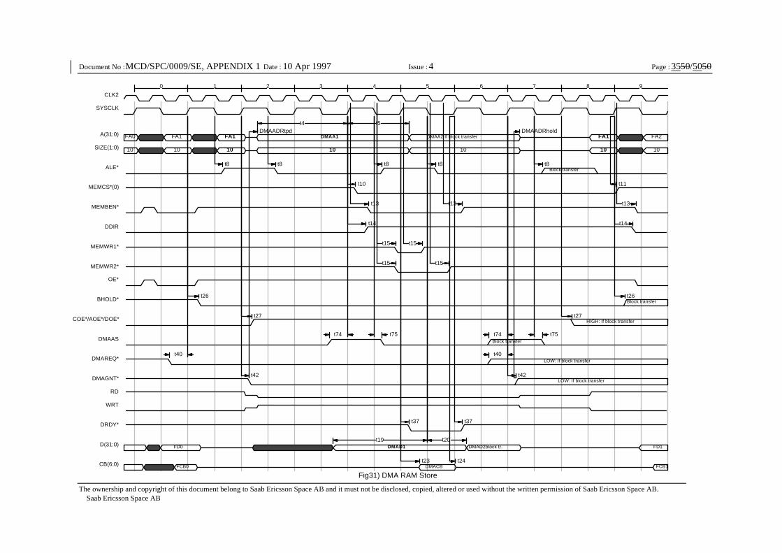
Page : 3550/5050
The ownership and copyright of this document belong to Saab Ericsson Space AB and it must not be disclosed, copied, altered or used without the written permission of Saab Ericsson Space AB. Saab Ericsson Space AB
Document No : MCD/SPC/0009/SE, APPENDIX 1 Date : 10 Apr 1997 Issue : 4
0 1 2 3 4 5 6 7 8 9
t4 t5
t74 t75 t74 t75
t40 t40
t19 t20
DMAADRtpd DMAADRhold
t8 t8 t8 t8 t8
t10 t11
t13 t13 t13
t14 t14
t15 t15
t15 t15
t26 t26
t27 t27
t42 t42
t37 t37
t23 t24
FA1 DMAA1 FA1
10 10 10
DMAD1
FA1
10 10
FA2
DMACB
FD0
FCB0
FA0
10
FD1
FCB1
LOW: If block transfer
HIGH: If block transfer
LOW: If block transfer
Block transfer
Block transfer
DMAA2 If block transfer
10
Block transfer
DMAD2block tr.
Fig31) DMA RAM Store
CLK2
SYSCLK
A(31:0)
SIZE(1:0)
ALE*
MEMCS*(0)
MEMBEN*
DDIR
MEMWR1*
MEMWR2*
OE*
BHOLD*
COE*/AOE*/DOE*
DMAAS
DMAREQ*
DMAGNT*
RD
WRT
DRDY*
D(31:0)
CB(6:0)
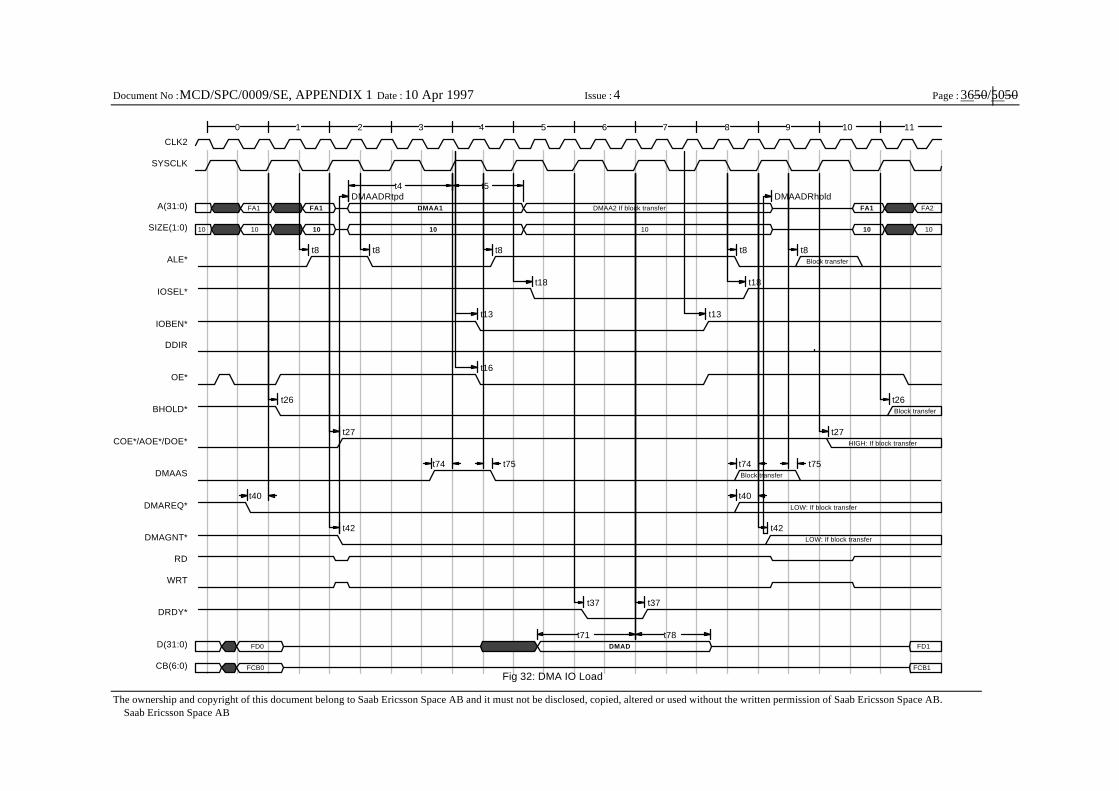
Page : 3650/5050
The ownership and copyright of this document belong to Saab Ericsson Space AB and it must not be disclosed, copied, altered or used without the written permission of Saab Ericsson Space AB. Saab Ericsson Space AB
Document No : MCD/SPC/0009/SE, APPENDIX 1 Date : 10 Apr 1997 Issue : 4
0 1 2 3 4 5 6 7 8 9 10 11
t4 t5
t74 t75 t74 t75
t40 t40
t71 t78
DMAADRtpd DMAADRhold
t8 t8 t8 t8 t8
t18 t18
t13 t13
t16
t26 t26
t27 t27
t42 t42
t37 t37
FA1 DMAA1 FA1
10 10 10
DMAD
FA1
10 10
FA2
FD0
FCB0
10
FD1
FCB1
LOW: If block transfer
HIGH: If block transfer
LOW: If block transfer
Block transfer
Block transfer
DMAA2 If block transfer
10
Block transfer
Fig 32: DMA IO Load
CLK2
SYSCLK
A(31:0)
SIZE(1:0)
ALE*
IOSEL*
IOBEN*
DDIR
OE*
BHOLD*
COE*/AOE*/DOE*
DMAAS
DMAREQ*
DMAGNT*
RD
WRT
DRDY*
D(31:0)
CB(6:0)
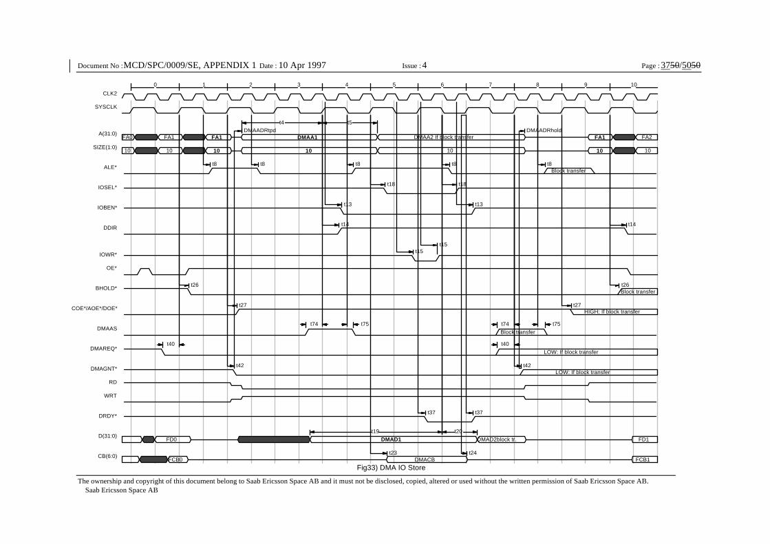
Page : 3750/5050
The ownership and copyright of this document belong to Saab Ericsson Space AB and it must not be disclosed, copied, altered or used without the written permission of Saab Ericsson Space AB. Saab Ericsson Space AB
Document No : MCD/SPC/0009/SE, APPENDIX 1 Date : 10 Apr 1997 Issue : 4
0 1 2 3 4 5 6 7 8 9 10
t4 t5
t74 t75 t74 t75
t40 t40
t19 t20
DMAADRtpd DMAADRhold
t8 t8 t8 t8 t8
t18 t18
t13 t13
t14 t14
t15t15
t26 t26
t27 t27
t42 t42
t37 t37
t23 t24
FA1 DMAA1 FA1
10 10 10
DMAD1
FA1
10 10
FA2
DMACB
FD0
FCB0
FA0
10
FD1
FCB1
LOW: If block transfer
HIGH: If block transfer
LOW: If block transfer
Block transfer
Block transfer
DMAA2 If block transfer
10
Block transfer
DMAD2block tr.
Fig33) DMA IO Store
CLK2
SYSCLK
A(31:0)
SIZE(1:0)
ALE*
IOSEL*
IOBEN*
DDIR
IOWR*
OE*
BHOLD*
COE*/AOE*/DOE*
DMAAS
DMAREQ*
DMAGNT*
RD
WRT
DRDY*
D(31:0)
CB(6:0)
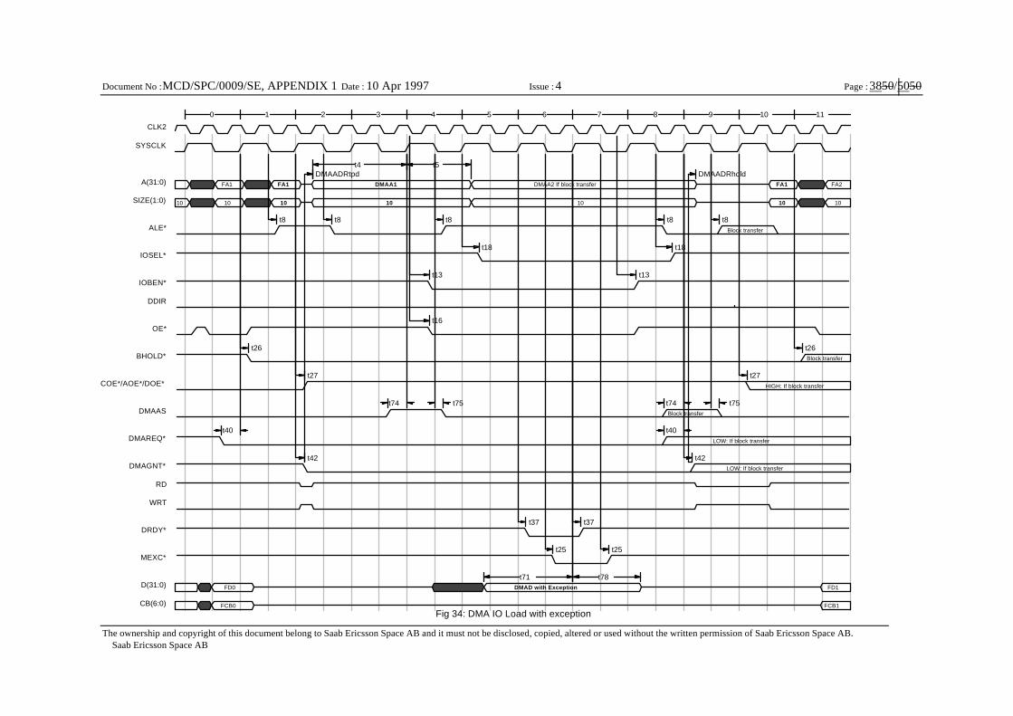
Page : 3850/5050
The ownership and copyright of this document belong to Saab Ericsson Space AB and it must not be disclosed, copied, altered or used without the written permission of Saab Ericsson Space AB. Saab Ericsson Space AB
Document No : MCD/SPC/0009/SE, APPENDIX 1 Date : 10 Apr 1997 Issue : 4
0 1 2 3 4 5 6 7 8 9 10 11
t4 t5
t74 t75 t74 t75
t40 t40
t71 t78
DMAADRtpd DMAADRhold
t8 t8 t8 t8 t8
t18 t18
t13 t13
t16
t26 t26
t27 t27
t42 t42
t37 t37
t25 t25
FA1 DMAA1 FA1
10 10 10
DMAD with Exception
FA1
10 10
FA2
FD0
FCB0
10
FD1
FCB1
LOW: If block transfer
HIGH: If block transfer
LOW: If block transfer
Block transfer
Block transfer
DMAA2 If block transfer
10
Block transfer
Fig 34: DMA IO Load with exception
CLK2
SYSCLK
A(31:0)
SIZE(1:0)
ALE*
IOSEL*
IOBEN*
DDIR
OE*
BHOLD*
COE*/AOE*/DOE*
DMAAS
DMAREQ*
DMAGNT*
RD
WRT
DRDY*
MEXC*
D(31:0)
CB(6:0)
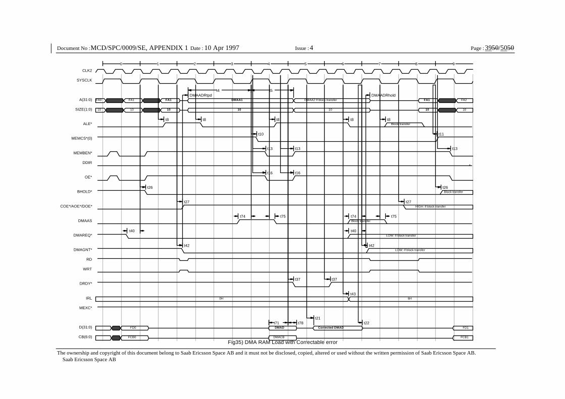
Page : 3950/5050
The ownership and copyright of this document belong to Saab Ericsson Space AB and it must not be disclosed, copied, altered or used without the written permission of Saab Ericsson Space AB. Saab Ericsson Space AB
Document No : MCD/SPC/0009/SE, APPENDIX 1 Date : 10 Apr 1997 Issue : 4
0 1 2 3 4 5 6 7 8 9
t4 t5
t74 t75 t74 t75
t40 t40
t71 t78
DMAADRtpd DMAADRhold
t8 t8 t8 t8 t8
t10 t11
t13 t13 t13
t16 t16
t26 t26
t27 t27
t42 t42
t37 t37
t43
t21t22
FA1 DMAA1 FA1
Corrected DMAD
10 10 10
DMAD
FA1
10 10
FA2
DMACB
FD0
FCB0
FA0
10
FD1
FCB1
LOW: If block transfer
HIGH: If block transfer
LOW: If block transfer
Block transfer
Block transfer
DMAA2 If block transfer
10
Block transfer
Fig35) DMA RAM Load with Correctable error
0H 6H
CLK2
SYSCLK
A(31:0)
SIZE(1:0)
ALE*
MEMCS*(0)
MEMBEN*
DDIR
OE*
BHOLD*
COE*/AOE*/DOE*
DMAAS
DMAREQ*
DMAGNT*
RD
WRT
DRDY*
IRL
MEXC*
D(31:0)
CB(6:0)
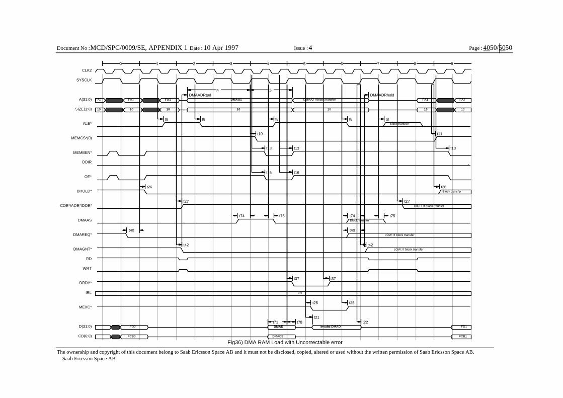
Page : 4050/5050
The ownership and copyright of this document belong to Saab Ericsson Space AB and it must not be disclosed, copied, altered or used without the written permission of Saab Ericsson Space AB. Saab Ericsson Space AB
Document No : MCD/SPC/0009/SE, APPENDIX 1 Date : 10 Apr 1997 Issue : 4
0 1 2 3 4 5 6 7 8 9
t4 t5
t74 t75 t74 t75
t40 t40
t71 t78
DMAADRtpd DMAADRhold
t8 t8 t8 t8 t8
t10 t11
t13 t13 t13
t16 t16
t26 t26
t27 t27
t42 t42
t37 t37
t25 t25
t21t22
FA1 DMAA1 FA1
Invalid DMAD
10 10 10
DMAD
FA1
10 10
FA2
DMACB
FD0
FCB0
FA0
10
FD1
FCB1
LOW: If block transfer
HIGH: If block transfer
LOW: If block transfer
Block transfer
Block transfer
DMAA2 If block transfer
10
Block transfer
Fig36) DMA RAM Load with Uncorrectable error
0H
CLK2
SYSCLK
A(31:0)
SIZE(1:0)
ALE*
MEMCS*(0)
MEMBEN*
DDIR
OE*
BHOLD*
COE*/AOE*/DOE*
DMAAS
DMAREQ*
DMAGNT*
RD
WRT
DRDY*
IRL
MEXC*
D(31:0)
CB(6:0)
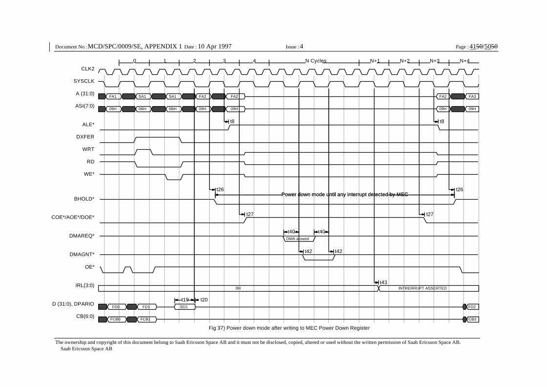
Page : 4150/5050
The ownership and copyright of this document belong to Saab Ericsson Space AB and it must not be disclosed, copied, altered or used without the written permission of Saab Ericsson Space AB. Saab Ericsson Space AB
Document No : MCD/SPC/0009/SE, APPENDIX 1 Date : 10 Apr 1997 Issue : 4
0 1 2 3 4 N Cycles N+1 N+2 N+3 N+4
Power down mode until any interrupt detected by MECPower down mode until any interrupt detected by MEC
t40 t40
t19 t20
t8 t8
t26 t26
t27 t27
t42 t42
t43
SA1 SA1 FA2
FD2
0BH 0BH 09H
SD1
Fig 37) Power down mode after writing to MEC Power Down Register
FA1
09H
FCB2
FD1FD0
FCB1FCB0
FA2
09H
0H INTRERRUPT ASSERTED
FA2 FA3
09H 09H
DMA alowed
CLK2
SYSCLK
A (31:0)
ASI(7:0)
ALE*
DXFER
WRT
RD
WE*
BHOLD*
COE*/AOE*/DOE*
DMAREQ*
DMAGNT*
OE*
IRL(3:0)
D (31:0), DPARIO
CB(6:0)
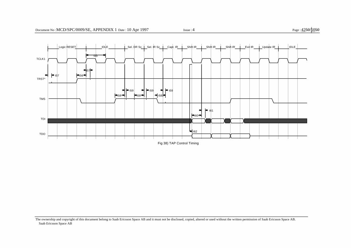
Page : 4250/5050
The ownership and copyright of this document belong to Saab Ericsson Space AB and it must not be disclosed, copied, altered or used without the written permission of Saab Ericsson Space AB. Saab Ericsson Space AB
Document No : MCD/SPC/0009/SE, APPENDIX 1 Date : 10 Apr 1997 Issue : 4
Logic RESET IDLE Sel. DR Sc. Sel. IR Sc. Capt. IR Shift IR Shift IR Shift IR Exit IR Update IR IDLE
t55t55
t57 t56
t57
t58
t59
t58
t59
t58
t59
t60
t61
t62
Fig 38) TAP Control Timing
TCLK1
TRST*
TMS
TDI
TDO
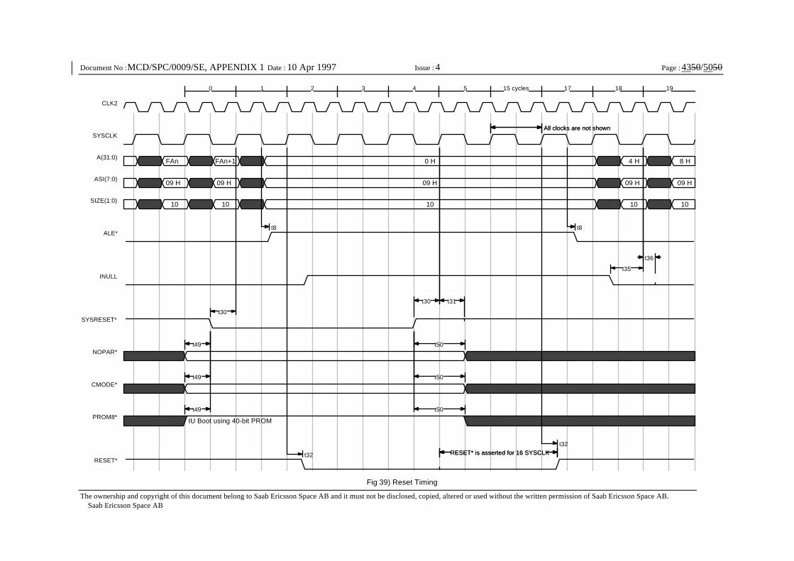
Page : 4350/5050
The ownership and copyright of this document belong to Saab Ericsson Space AB and it must not be disclosed, copied, altered or used without the written permission of Saab Ericsson Space AB. Saab Ericsson Space AB
Document No : MCD/SPC/0009/SE, APPENDIX 1 Date : 10 Apr 1997 Issue : 4
0 1 2 3 4 5 15 cycles 17 18 19
All clocks are not shownAll clocks are not shown
t35
t36
t30
t30 t31
t49 t50
t49 t50
t49 t50
RESET* is asserted for 16 SYSCLKRESET* is asserted for 16 SYSCLK
t8 t8
t32
t32
0 H
09 H
10 10
4 H 8 H
09 H 09 H
10 10
09 H
FAn+1FAn
09 H
10
Fig 39) Reset Timing
IU Boot using 40-bit PROM
CLK2
SYSCLK
A(31:0)
ASI(7:0)
SIZE(1:0)
ALE*
INULL
SYSRESET*
NOPAR*
CMODE*
PROM8*
RESET*
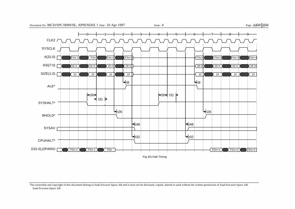
Page : 4450/5050
The ownership and copyright of this document belong to Saab Ericsson Space AB and it must not be disclosed, copied, altered or used without the written permission of Saab Ericsson Space AB. Saab Ericsson Space AB
Document No : MCD/SPC/0009/SE, APPENDIX 1 Date : 10 Apr 1997 Issue : 4
0 1 2 3 4 5 6 7 8 9
t30t31
t30 t31
t8 t8
t26 t26
t48 t48
t32 t32
10
FAn+3 FAn+4
09 H 09 H
10 10
09 H
FAnFAn-1
09 H
10
Fig 40) Halt Timing
FAn+1
09 H
10
FAn+1
09 H
10
FDn-2 FDn-1 FDn
FAn+1 FAn+2
09 H 09 H
10 10
FDn+1 FDn+2 FDn+3
CLK2
SYSCLK
A(31:0)
ASI(7:0)
SIZE(1:0)
ALE*
SYSHALT*
BHOLD*
SYSAV
CPUHALT*
D31:0),DPARIO
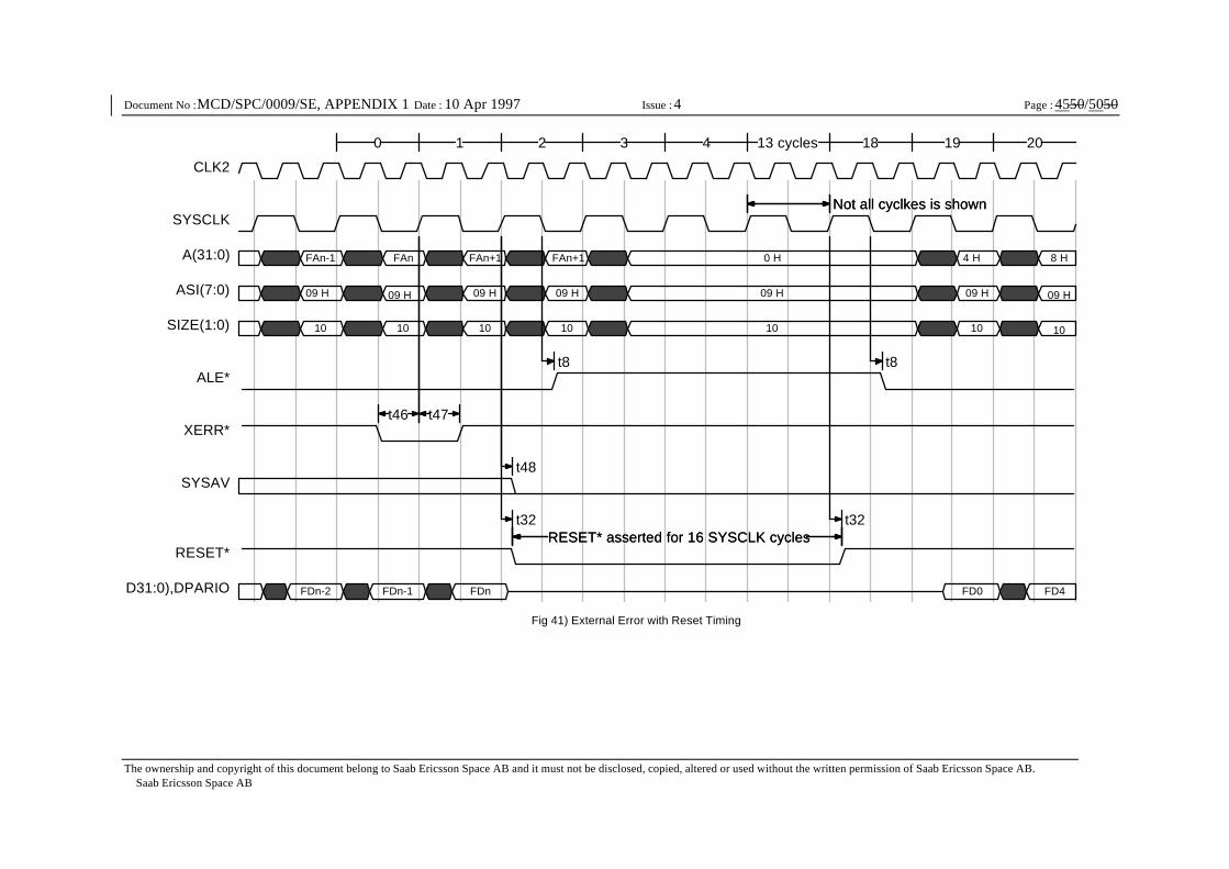
Page : 4550/5050
The ownership and copyright of this document belong to Saab Ericsson Space AB and it must not be disclosed, copied, altered or used without the written permission of Saab Ericsson Space AB. Saab Ericsson Space AB
Document No : MCD/SPC/0009/SE, APPENDIX 1 Date : 10 Apr 1997 Issue : 4
0 1 2 3 4 13 cycles 18 19 20
Not all cyclkes is shownNot all cyclkes is shown
t46 t47
RESET* asserted for 16 SYSCLK cyclesRESET* asserted for 16 SYSCLK cycles
t8 t8
t48
t32 t32
10
8 H
09 H
10
09 H
FAnFAn-1
09 H
10
Fig 41) External Error with Reset Timing
FAn+1
09 H
10
FAn+1
09 H
10
FDn-2 FDn-1 FDn
0 H 4 H
09 H 09 H
10 10
FD0 FD4
CLK2
SYSCLK
A(31:0)
ASI(7:0)
SIZE(1:0)
ALE*
XERR*
SYSAV
RESET*
D31:0),DPARIO
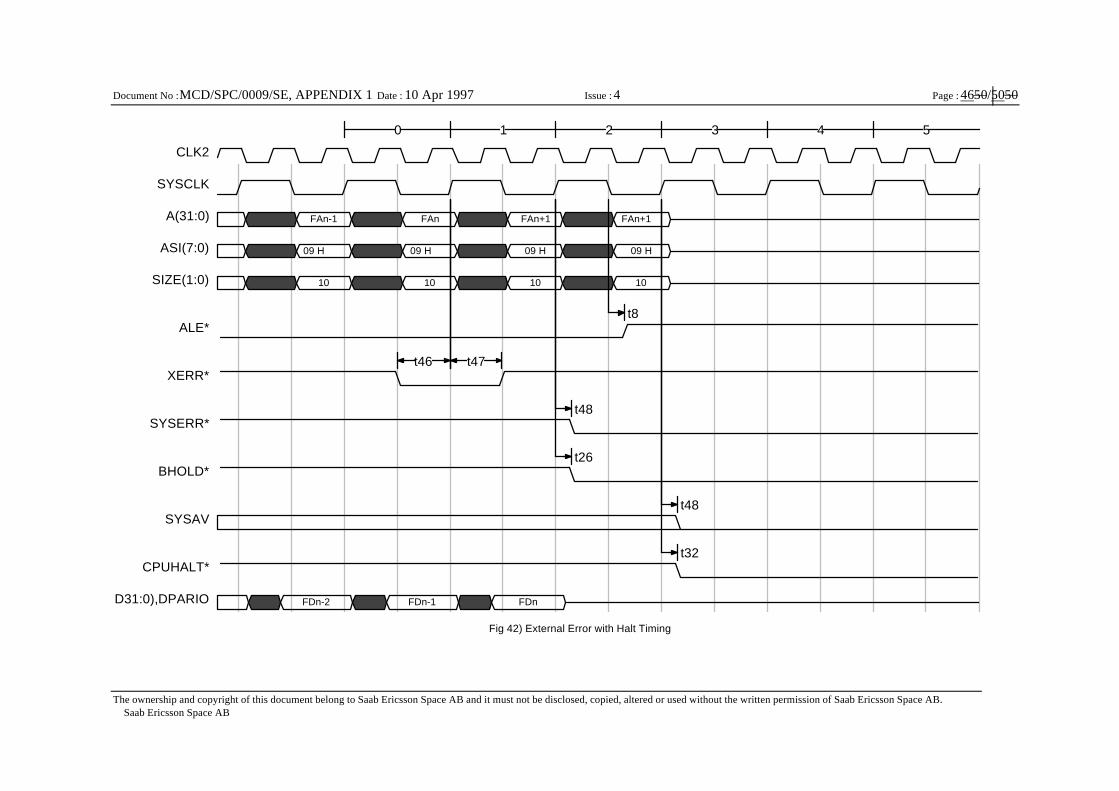
Page : 4650/5050
The ownership and copyright of this document belong to Saab Ericsson Space AB and it must not be disclosed, copied, altered or used without the written permission of Saab Ericsson Space AB. Saab Ericsson Space AB
Document No : MCD/SPC/0009/SE, APPENDIX 1 Date : 10 Apr 1997 Issue : 4
0 1 2 3 4 5
t46 t47
t8
t48
t26
t48
t32
10
09 H
FAnFAn-1
09 H
10
Fig 42) External Error with Halt Timing
FAn+1
09 H
10
FAn+1
09 H
10
FDn-2 FDn-1 FDn
CLK2
SYSCLK
A(31:0)
ASI(7:0)
SIZE(1:0)
ALE*
XERR*
SYSERR*
BHOLD*
SYSAV
CPUHALT*
D31:0),DPARIO
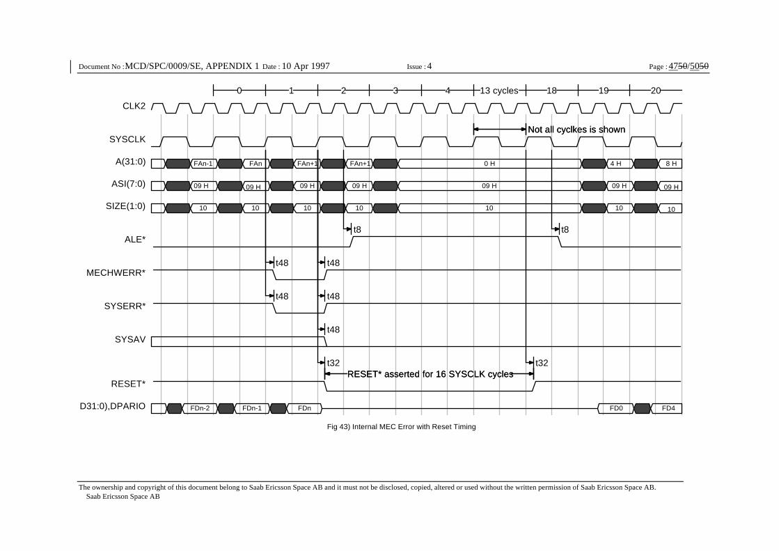
Page : 4750/5050
The ownership and copyright of this document belong to Saab Ericsson Space AB and it must not be disclosed, copied, altered or used without the written permission of Saab Ericsson Space AB. Saab Ericsson Space AB
Document No : MCD/SPC/0009/SE, APPENDIX 1 Date : 10 Apr 1997 Issue : 4
0 1 2 3 4 13 cycles 18 19 20
Not all cyclkes is shownNot all cyclkes is shown
RESET* asserted for 16 SYSCLK cyclesRESET* asserted for 16 SYSCLK cycles
t8 t8
t48 t48
t48 t48
t48
t32 t32
10
8 H
09 H
10
09 H
FAnFAn-1
09 H
10
Fig 43) Internal MEC Error with Reset Timing
FAn+1
09 H
10
FAn+1
09 H
10
FDn-2 FDn-1 FDn
0 H 4 H
09 H 09 H
10 10
FD0 FD4
CLK2
SYSCLK
A(31:0)
ASI(7:0)
SIZE(1:0)
ALE*
MECHWERR*
SYSERR*
SYSAV
RESET*
D31:0),DPARIO

Page : 4850/5050
The ownership and copyright of this document belong to Saab Ericsson Space AB and it must not be disclosed, copied, altered or used without the written permission of Saab Ericsson Space AB. Saab Ericsson Space AB
Document No : MCD/SPC/0009/SE, APPENDIX 1 Date : 10 Apr 1997 Issue : 4
0 1 2 3 4 5
t8
t48
t48
t26
t48
t32
10
09 H
FAnFAn-1
09 H
10
Fig 44) Internal MEC Error with Halt Timing
FAn+1
09 H
10
FAn+1
09 H
10
FDn-2 FDn-1 FDn
CLK2
SYSCLK
A(31:0)
ASI(7:0)
SIZE(1:0)
ALE*
MECHWERR*
SYSERR*
BHOLD*
SYSAV
CPUHALT*
D31:0),DPARIO
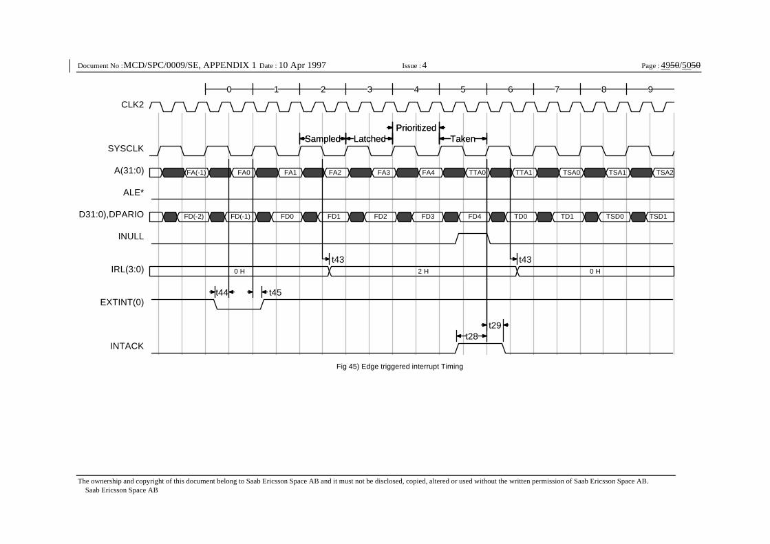
Page : 4950/5050
The ownership and copyright of this document belong to Saab Ericsson Space AB and it must not be disclosed, copied, altered or used without the written permission of Saab Ericsson Space AB. Saab Ericsson Space AB
Document No : MCD/SPC/0009/SE, APPENDIX 1 Date : 10 Apr 1997 Issue : 4
0 1 2 3 4 5 6 7 8 9
Sampled LatchedSampledPrioritized
Latched TakenPrioritized
Taken
t44 t45
t28t29
t43 t43
TSA1 TSA2FA0FA(-1)
Fig 45) Edge triggered interrupt Timing
FA1 FA2
FD(-2) FD(-1) FD0
TTA1 TSA0
TD1 TSD0 TSD1
0 H 2 H 0 H
FD1 FD2 FD3 FD4
FA3 FA4 TTA0
TD0
CLK2
SYSCLK
A(31:0)
ALE*
D31:0),DPARIO
INULL
IRL(3:0)
EXTINT(0)
INTACK
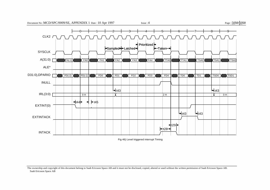
Page : 5050/5050
The ownership and copyright of this document belong to Saab Ericsson Space AB and it must not be disclosed, copied, altered or used without the written permission of Saab Ericsson Space AB. Saab Ericsson Space AB
Document No : MCD/SPC/0009/SE, APPENDIX 1 Date : 10 Apr 1997 Issue : 4
0 1 2 3 4 5 6 7 8 9
Sampled LatchedSampledPrioritized
Latched TakenPrioritized
Taken
t44 t45
t28t29
t43 t43
t43 t43
TSA1 TSA2FA0FA(-1)
Fig 46) Level triggered interrupt Timing
FA1 FA2
FD(-2) FD(-1) FD0
TTA1 TSA0
TD1 TSD0 TSD1
0 H 2 H 0 H
FD1 FD2 FD3 FD4
FA3 FA4 TTA0
TD0
CLK2
SYSCLK
A(31:0)
ALE*
D31:0),DPARIO
INULL
IRL(3:0)
EXTINT(0)
EXTINTACK
INTACK