Embed Size (px)
Citation preview

1
Susam Pal
Project Author
Roll No. 11550
8th Semester (2005)
Electronics and Telecommunication Engineering
Anil Kumar Patro
Lecturer & Project Advisor Electronics and Telecommunication Engineering
Kalinga Institute of Industrial Technology University

2
1. Design Tools
A lot of tools and a few languages are available for chip designing. The tools and a
language chosen by an individual or an organization for chip designing depend on the
requirement and taste of the individual or organization. This section describes the tools
and the language used to design the 16-bit microprocessor in this project.
1.1 Xilinx XC9572 PC84 CPLD Trainer
The microprocessor was designed in a trainer kit containing a Xilinx CPLD chip. The
trainer belongs to the device family, XC9500 CPLDs. The device is called XC9572.
Figure 1.1 shows a picture of the trainer.
Figure 1.1 Xilinx XC9572 PC84 CPLD Trainer
The features of the trainer are as follows:-
i. 84 pin PLCC socket for XC9572 PC84 CPLD device.
ii. Additional 44 pin PLCC socket for programming of XC9572 PC44 device.
iii. On board power supply with a polarity free power connector.
iv. On board 4 MHz clock and Power On reset circuit.
v. 16 Digital I/Ps and O/Ps with LED indication.
vi. Four seven segment Multiplexed Displays.
vii. User selectable interface hardware.
viii. Probing facility: All I/O’s of the device are accessible to the user for external use
ix. Compatible with Xilinx Foundation Series Software
1.2 Xilinx Project Navigator
Xilinx Project Navigator is a software provided by Xilinx to configure the Xilinx CPLD
devices. A project is created using this software and the source code of the design is
added to the project. Then the code is synthesized and implemented for the device.
3
Finally the chip is configured with the help of the software.
Xilinx Project Navigator provides an integrated development environment with an editor
to edit the source code. Project Navigator also provides a fitter report when a design is
implemented. The fitter report contains information of the usage of the various trainer
resources. In case the design is too large to fit into the chip, the implementation ends up
in a failure. In such a case the fitter report can be seen to get an idea of how large is the
design and how much optimization needs to be done in order to fit the design into the
chip.
If ModelSim is installed in the computer, it can be invoked from within the Xilinx Project
Navigator. It can synthesize codes written in languages like VHDL and Verilog.
1.3 ModelSim
Before the chip is configured as per the source code, the function of the design formed
due to the source code must be observed and analyzed for errors. ModelSim is a software
which is used to simulate the operation of the design. One can set the different signals,
provide clock and observe the various signals and outputs as waveforms. These
waveforms can be used to check if the design is working as was intended and debug the
source code in case the design is not working properly.
ModelSim also contains its own integrated development environment with an editor. It
has various other windows where one can set signals and observe the waveforms.
1.4 VHDL
VHDL is an acronym for VHSIC Hardware Description Language. VHSIC in turn is an
acronym for Very High Speed Integrated Circuits. It is a hardware description language
that is used to model a digital system at many levels of abstraction, ranging from the
algorithmic level to the gate level. The complexity of the digital system being modeled
could vary from that of a simple gate to a complete digital electronic system, or anything
in between. The digital system can also be described hierarchically. Timing can also be
explicitly modeled in the same description though it can’t be synthesized with the Xilinx
Project Navigator.
The code to model the microprocessor was written in this language and then added to a
project in the Xilinx Project Navigator to synthesize, implement and configure the chip.

4
2. Introduction
Most microprocessors use the stored-program concept designed by Hungarian
mathematician John Von Neumann. This is also known as Von Neumann architecture. It
is a model of computing machine that uses a single storage structure to hold both the set
of instructions on how to perform the computation and the data required or generated by
the computation. The separation of storage from processing unit is implicit in this model.
In this project a processor based on stored-program concept has been designed.
2.1 Stored Program Organization
A processor based on Von Neumann architecture performs or emulates the following
sequence of steps:-
i. Fetches the next instruction from memory at the address in the program counter.
ii. Increments the program counter by 1.
iii. Decodes the instruction using the control unit. The control unit issues necessary
signals to command other components to carry out the instruction. The instruction
may change the address in the program counter, permitting repetitive operations.
The instruction may also change the program counter only if some arithmetic
condition is true, thus permitting decision making, which can be calculated to any
degree of complexity by the preceding arithmetic and logical instructions.
iv. Repeat step i. to step iii.
The processor designed in this project doesn’t have a pure Von Neumann architecture as
it adds another step to check for interrupts. When an interrupt occurs, the usual way of
executing the instructions is suspended and the control is transferred to an interrupt
service routine.
It has one processor register and an instruction code format with two parts. The first part
specifies the operation to be performed and the second specifies an address. The memory
address tells the control where to find an operand in memory. This operand is read from
memory and used as the data to be operated on together with the data stored in the
processor register.
A 16-bit memory unit with 4096 words can be addressed by the microprocessor. Thus the
microprocessor needs 12 address lines to address the memory unit with 4096 (= 212)
words. As each instruction is stored in one 16-bit memory word, four bits are available
for the operation code (abbreviated opcode) to specify one out of 16 possible operations,
and 12 bits to specify the address of an operand. The control reads a 16-bit instruction
from the program portion of memory. It uses the 12-bit address part of the instruction to
read a 16-bit operand from the data portion of memory. It then executes the operation
specified by the operation code.
As the processor has a single-processor register it is named as accumulator and is labeled
as AC. The operation is performed with the memory operand and the content of
accumulator (AC).

5
Figure 2.1: Stored program organization
As the processor has a single-processor register it is named as accumulator and is labeled
as AC. The operation is performed with the memory operand and the content of
accumulator (AC).
If an operation in an instruction code does not need an operand from memory, the rest of
the bits in the instruction can be used for other purposes. For example, operations such as
clear AC, complement AC and increment AC operate on data stored in the AC register.
They do not need an operand from memory. For these types of operations, the second part
of the instruction code (bits 0 through 11) is not needed for specifying a memory address
and is used to specify other operations for the processor.
Opcode Address
Binary Operand
15 12 11 0
15 0
Instructions
(program)
Operands
(data)
Instruction format
Memory
4096 × 16
Processor register (accumulator or AC)
15 0
6
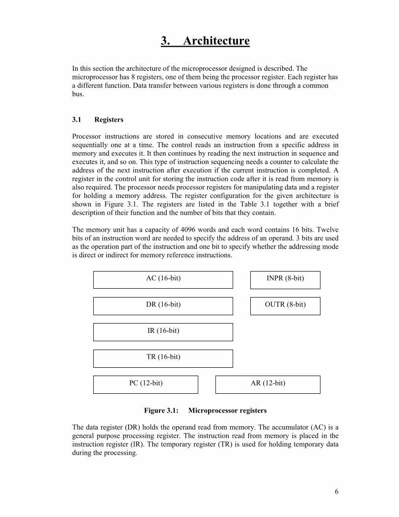
3. Architecture
In this section the architecture of the microprocessor designed is described. The
microprocessor has 8 registers, one of them being the processor register. Each register has
a different function. Data transfer between various registers is done through a common
bus.
3.1 Registers
Processor instructions are stored in consecutive memory locations and are executed
sequentially one at a time. The control reads an instruction from a specific address in
memory and executes it. It then continues by reading the next instruction in sequence and
executes it, and so on. This type of instruction sequencing needs a counter to calculate the
address of the next instruction after execution if the current instruction is completed. A
register in the control unit for storing the instruction code after it is read from memory is
also required. The processor needs processor registers for manipulating data and a register
for holding a memory address. The register configuration for the given architecture is
shown in Figure 3.1. The registers are listed in the Table 3.1 together with a brief
description of their function and the number of bits that they contain.
The memory unit has a capacity of 4096 words and each word contains 16 bits. Twelve
bits of an instruction word are needed to specify the address of an operand. 3 bits are used
as the operation part of the instruction and one bit to specify whether the addressing mode
is direct or indirect for memory reference instructions.
Figure 3.1: Microprocessor registers
The data register (DR) holds the operand read from memory. The accumulator (AC) is a
general purpose processing register. The instruction read from memory is placed in the
instruction register (IR). The temporary register (TR) is used for holding temporary data
during the processing.
AC (16-bit)
DR (16-bit)
IR (16-bit)
TR (16-bit)
PC (12-bit) AR (12-bit)
INPR (8-bit)
OUTR (8-bit)
7
The memory address register (AR) has 12 bits since this is the width of a memory
address. The program counter (PC) also has 12 bits and it holds the address of the next
instruction to be read from memory after the current instruction is executed. The PC goes
through a counting sequence and causes the computer to read sequential instructions
previously stored in memory. Instruction words are read and executed in sequence unless
a branch instruction is encountered. A branch instruction calls for a transfer to a
nonconsecutive instruction in the program. The address part of a branch instruction is
transferred to PC to become the address of the next instruction. To read an instruction, the
content of PC is taken as the address for memory and a memory read cycle is initiated.
The PC is then incremented by one, so it holds the address of the next instruction in
sequence.
Two registers are used for input and output. The input register (INPR) receives an 8-bit
character from an input device. The output register (OUTR) holds an 8-bit character for
an output device.
Register
symbol
Number
of bits
Register name Function
DR
AR
AC
IR
PC
TR
INPR
OUTR
16
12
16
16
12
16
8
8
Data register
Address register
Accumulator
Instruction register
Program counter
Temporary register
Input register
Output register
Holds memory operand
Holds address for memory
Processor register
Holds instruction code
Holds address of instruction
Holds temporary data
Holds input character
Holds output character
Table 3.1 List of registers
3.2 Common Bus System
The processor has eight registers and a control unit. A path needs to be provided to
transfer information from one register to another and between memory and registers. An
efficient scheme of common bus is used for transferring information in this system.
Number of wires and connections is reduced in this approach. In this approach all the
registers transfer data between themselves through a common bus.

8
4. Timing and Control
The timing and control unit is the most important part of the microprocessor. A sequence
counter and a decoder together form the timing unit. It issues timing signals, which
informs the control unit of the current state of execution of instruction. The control unit
comprises of control logic gates, instruction decoder, flip-flops and the timing unit. The
control unit issues signals for various components of the microprocessor. It issues the
necessary signals depending on the timing signal and the instruction fetched in the
instruction decoder.
4.1 Timing Unit
The microprocessor performs some microoperations every at every clock pulse. The
sequence counter (SC) counts from 00002 to 11112. The output of the sequence counter is
fed to a 4 × 16 decoder which decodes the input binary number and generates a timing
signal which will be called T0, T1 and so on in the sections to follow. Thus the timing unit
generates a new timing signal every clock cycle. The SC can be incremented or cleared
synchronously. Most of the time, the counter is incremented to provide the sequence of
timing signals out of the 4 × 16 decoder. The control unit starts fetching an instruction
with the timing signal T0. The control unit performs various steps to execute the fetched
instruction at each timing signal. Various instructions can take various numbers of timing
signals. At the end of the instruction cycle the counter is cleared to 0, causing the next
active timing signal to be T0 so that a new instruction cycle can start.
The timing diagram of Figure 4.1 shows the time relationship of the control signals.
When the ‘reset’ signal is high, the ‘clr_sc’ signal remains high and the SC is cleared to
00002 and no timing signal is generated. When the ‘reset’ signal is made low, ‘clr_sc’
also turns low and the timing signal is generated at the positive transition of the clock
pulse. The SC responds to the positive transition of the clock. T0 is active during one
clock cycle. The timing signal T0 will trigger only those registers whose control inputs are
connected to timing signal T0. SC is incremented with every positive clock transition,
unless ‘clr_sc’ signal is active. This produces a sequence of timing signals T0, T1, T2, T3,
and so on, as shown in Figure 4.1. If SC is not cleared, the timing signals will continue
with T7, T8 to T15 and back to T0. For instance, a memory read or memory write cycle will
be initiated with the rising edge of a timing signal. The memory read cycle time is less
than the clock cycle time. Accordingly, a memory read cycle initiated by a timing signal
will be completed by the time next clock goes through its positive transition. The clock
transition will then be used to load the memory word into a register.
The timing diagram of Figure 4.1 shows the time relationship of the control signals.
When the ‘reset’ signal is high, the ‘clr_sc’ signal remains high and the SC is cleared to
00002 and no timing signal is generated. When the ‘reset’ signal is made low, ‘clr_sc’
also turns low and the timing signal is generated at the positive transition of the clock
pulse. The SC responds to the positive transition of the clock. T0 is active during one
clock cycle. The timing signal T0 will trigger only those registers whose control inputs are
connected to timing signal T0. SC is incremented with every positive clock transition,
unless ‘clr_sc’ signal is active. This produces a sequence of timing signals T0, T1, T2, T3,
and so on, as shown in Figure 4.1. If SC is not cleared, the timing signals will continue
with T7, T8 to T15 and back to T0.

9
Figure 4.1
Example of control timing signals

10
For instance, a memory read or memory write cycle will be initiated with the rising edge
of a timing signal. The memory read cycle time is less than the clock cycle time.
Accordingly, a memory read cycle initiated by a timing signal will be completed by the
time next clock goes through its positive transition. The clock transition will then be used
to load the memory word into a register.
4.2 Control Unit
The block diagram of the control unit is shown in Figure 4.2. It consists of two decoders,
a sequence counter, and a number of control logic gates. An instruction read from
memory is placed in the instruction register (IR), where it is divided into three parts: the I
bit, the operation code, and bits 11 through 0. The I bit is the most significant bit (MSB)
of the instruction code. The I bit is stored in I flip-flop. The operation code in the bits 12
through 14 are decoded with a 3 × 8 decoder. The eight outputs of the decoder are
designated by the symbols D0 through D7. The output of the decoder specifies the
operation to be done. The subscripted decimal number is equivalent to the binary value of
the corresponding operation code. Bit 15 of the instruction is transferred to the control
logic gates.

11
Figure 4.2 Control unit
The control logic gates perform the necessary microoperations to complete the instruction
depending on the timing signals, the I flip-flop and the decoder output. The bits 11
through 0 contain the address of the operand or the type of instruction in register
reference instructions and input-output instructions, which is used by the control unit for
its operation.
15 14 13 12 11 – 0
3 × 8 decoder
7 6 5 4 3 2 1 0
I
Control
logic
gates
15 14 - - - - - - - - 1 0
4 × 16 decoder
4-bit sequence
counter
(SC)
Other inputs
D0
D7
T15
T0
Increment
Clock
Clear
Instruction Decoder
Control
outputs

12
5. Instructions
The processor instructions are of 16 bits. Only three bits of the instruction is used for the
operation code. However, since register reference and input output instructions use the
remaining 12 bits as a part of the operation code, the total number of instructions exceeds
eight. Its instruction set consists of 25 instructions.
5.1 Instruction Formats
The processor has three instruction formats. Each format has 16 bits. The operation code
part of the instruction contains three bits and the meaning of the remaining 13 bits
depends on the operation code encountered.
The instruction formats are:
i. Memory reference instruction
ii. Register reference instruction
iii. Input output instruction
Figure 5.1 Instruction formats
The type of instruction is recognized by the processor control from the four bits in
positions 12 through 15 of the instruction. If the three opcode bits in positions 12 through
14 are not equal to 111, the instruction is a memory reference type and the bit position 15
is taken as the addressing mode I. If the 3-bit opcode is equal to 111, control then inspects
the bit 15. If this bit is 0, the instruction is a register–reference type. If the bit is 1, the
instruction is an input output type.
5.1.1 Memory reference instructions
A memory reference instruction uses the most significant bit (MSB) of the instruction
I Opcode Address
0 1 1 1 Register operation
1 1 1 1 Input output operation
Memory reference instruction
Register reference instruction
Input output instruction
13
code to specify the addressing mode in a memory reference instruction. This bit known as
the I bit. It is 0 if it is direct addressing mode and 1 if it is indirect addressing mode. The
bits 14 through 12 specify the opcode of the memory reference instruction. In a memory
reference instruction these bits can have a value between 0002 and 1102. Thus there are
seven kinds of memory reference instructions.
5.1.2 Register reference instructions
A register reference instruction specifies an operation on or a test of the AC register or the
E flip-flop. One of the instructions sets the S flip-flop called the stop flip-flop to stop the
operation of the microprocessor. It is recognized by the operation code 1112 with a 0 in
the leftmost bit (bit 15) of the instruction. An operand from memory is not needed.
Therefore, the other 12 bits are used to specify the operation or test to be executed.
5.1.3 Input output instructions
An input output instruction does not need a reference to memory and is recognized by the
operation code 1112 with a 1 in the leftmost bit of the instruction. The remaining12 bits
are used to specify the type of input output operation or test performed.
5.2 Addressing Modes
The different modes by which the microprocessor addresses the operands are known as
addressing modes. This microprocessor supports 3 addressing modes.
i. Direct memory addressing
ii. Indirect memory addressing
iii. Implicit addressing
In direct memory addressing the address of the operand is specified directly in the
instruction. In indirect memory addressing the address of the location where the address
of the operand can be found is specified in the instruction. In implicit addressing the
address of the operand is not specified. It is implicitly understood from the instruction.
There are certain instructions those act on specific operands like accumulator (AC) or
extended accumulator flip-flop (E).
5.3 Instruction Set
The processor can handle a sufficient number of instructions in each of the following
categories:
i. Arithmetic, logical and shift instructions
ii. Transfer instructions
iii. Program control instructions
iv. Input and output instructions
The instructions listed in Table 5.1 constitute a minimum set that provides all the

14
capabilities mentioned above. These instructions can be combined efficiently to perform a
variety of operations. For example ADD, CMA and INC can be combined together to add
and subtract binary numbers when negative numbers are in signed 2’s complement
representation. The circulate instructions CIR and CIL can be used for arithmetic shifts as
well as any other type of shifts desired. Multiplication and division can be performed
using addition, subtraction and shifting. There are three logical operations AND, CMA
and CLA. The AND and CMA provides a NAND operation. It can be shown that with the
NAND operation it is possible to implement all other logical operations with two
variables. Moving information from memory to AC is accomplished with the LDA
instruction. Storing information from AC into memory is done with the STA instruction.
The branch instructions BUN, BSA and ISZ together with the four skip instructions
provide capabilities for program control and checking of status conditions. The INP and
OUT instructions are used to transfer information between the processor and external
devices.
Symbol
Hexadecimal code
Description I = 0 I = 1
AND
ADD
LDA
STA
BUN
BSA
ISZ
0xxx
1xxx
2xxx
3xxx
4xxx
5xxx
6xxx
8xxx
9xxx
Axxx
Bxxx
Cxxx
Dxxx
Exxx
AND memory word to AC
Add memory word to AC
Load memory word to AC
Store content of AC in memory
Branch unconditionally
Branch and save return address
Increment and skip if zero
CLA
CLE
CLA
CME
CIR
CIL
INC
SPA
SNA
SZA
SZE
HLT
7800
7400
7200
7100
7080
7040
7020
7010
7008
7004
7002
7001
Clear AC
Clear E
Clear AC
Complement E
Circulate right AC and E
Circulate left AC and E
Increment AC
Skip next instruction if AC positive
Skip next instruction if AC negative
Skip next instruction if AC zero
Skip next instruction if E zero
Halt
INP
OUT
SKI
SKO
ION
IOF
F800
F400
F200
F100
F080
F040
Input character to AC
Output character from AC
Skip on input flag
Skip on output flag
Interrupt on
Interrupt off
Table 5.1 Instruction set
5.3.1 Arithmetic, logical and shift instructions
These instructions provide computational capabilities for processing the type of data that
the user may wish to employ. The arithmetic, logical and shift instructions in this
microprocessor are as follows.

15
Arithmetic instructions: ADD, INC
Logical instructions: AND, CLA, CLE, CMA, CME
Shift instructions: CIR, CIL
5.3.2 Transfer instructions
The bulk of the binary information required by the processor is stored in memory, but all
the computations are done in the processor registers. These instructions provide the
facility for moving information from memory and processor registers. The transfer
instructions in this microprocessor are: LDA, STA.
5.3.3 Program control instructions
These instructions provide the decision-making capability to the processor. These enable
the processor to behave differently in different situations. Some of these instructions
change the sequence in which the program is executed and some of them check certain
conditions. Examples of the instructions of this type are: BUN, BSA, ISZ, SPA, SNA,
SZA, SZE, HLT, SKI, SKO, ION, IOF.
5.3.4 Input output instructions
Programs and data need to be transferred into memory and results of computations need
to be transferred back to the user. Input and output instructions are needed for this
purpose. These instructions carry out the communication between the computer and the
user. Examples of the instructions of this type are: INP, OUT.

16
6. Instruction Cycle
A program residing in the memory unit of the computer consists of a sequence of
instructions. The program is executed in the computer by going through a cycle for each
instruction. Each instruction cycle in turn is subdivided into a sequence of sub-cycles or
phases. In the processor each instruction cycle consists of the following phases:
i. Fetch an instruction from memory.
ii. Decode the instruction.
iii. Read the effective address from memory if the instruction has an indirect address.
iv. Execute the instruction.
Upon the completion of step 4, the control goes back to step 1 to fetch, decode, and
execute the next instruction. This process continues indefinitely unless an HLT
instruction is encountered.
6.1 Fetch and Decode
Initially, the program counter PC is loaded with the address of the first instruction in the
program. The sequence counter SC is cleared to 0, providing a decoded timing signal T0.
After each clock pulse, SC is incremented by one, so that the timing signals go through a
sequence T0, T1, T2, and so on. The microoperations for the fetch and decode phases can
be specified by the following register transfer statements.
T0: AR ← PC, data ← M[AR]
T1: IR ← data, PC ← PC+1
T2: D0,…, D7 ← Decode IR(12-14), AR ← IR(0-11), I ←IR(15)
Since only AR is connected to the address lines which are connected to the address inputs
of memory, address from PC is transferred to AR during the clock transition associated
with timing signal T0. The instruction read from memory is obtained in the data lines of
the microprocessor before the next timing signal. The instruction is then placed in the
instruction register IR with the clock transition associated with timing signal T1. At the
same time, PC is incremented by one to prepare it for the address of the next instruction
in the program. At time T2, the operation code in IR is decoded, the indirect bit is
transferred to I flip-flop and the address part of the instruction is transferred to AR.
The timing signal that is active after the decoding is T3. During time T3 the control unit
determines the type of instruction that was just read from memory. Figure 6.1 presents an
initial configuration for the instruction cycle and shows how the control determines the
instruction type after the decoding.
Decoder output D7 is equal to 1 if the operation code is equal to 1112. If D7 = 1 the
instruction must be a register reference or input output type. If D7 = 0 the operation code
must be one of the other seven values 0002 through 1102, specifying a memory reference
instruction. Control then inspects the value of the first bit of the instruction, which is now
available in I, flip-flop. If D7 = 0 and I = 1, it is a memory reference instruction with an
indirect address. It is then necessary to read the effective address from memory. The
microperation for the indirect address condition can be symbolized by the register transfer

17
statements:-
data ← M[AR]
AR ← data
Figure 6.1 Flowchart for instruction cycle (initial configuration)
Decoder output D7 is equal to 1 if the operation code is equal to 1112. If D7 = 1 the
instruction must be a register reference or input output type. If D7 = 0 the operation code
must be one of the other seven values 0002 through 1102, specifying a memory reference
instruction. Control then inspects the value of the first bit of the instruction, which is now
available in I, flip-flop. If D7 = 0 and I = 1, it is a memory reference instruction with an
indirect address. It is then necessary to read the effective address from memory. The
microperation for the indirect address condition can be symbolized by the register transfer
statements:-
data ← M[AR]
AR ← data
Start
SC ← 0
AR ← PC
data ← M[AR]
IR ← data
PC ← PC + 1
D0,…D7 ← Decode IR(12-14)
AR ← IR(0-11), I ← IR(15)
D7
I I
Nothing data ← M[AR]
Execute register
reference
instruction
Execute input
output
instruction
SC ← 0 Execute memory reference instruction
SC ← 0
AR ← data
T0
T2
T1
Nothing
T3 T3
T4 T4
T3 T3
I = 0 I = 1 I = 0 I = 1
D7 = 0 D7 = 1 Register or I/O Memory reference
Register I/O Direct Indirect

18
Initially, AR holds the address part of the instruction. This address is used during the
memory read operation. The word at the address given by AR is read from memory and
placed on the common bus. The indirect address that resided in the 12 least significant
bits of the memory word is received.
The three instruction types are subdivided into four separate paths. The selected operation
is activated with the clock transition associated with timing signal T3. This can be
symbolized as follows.
D7’IT3: data ← M[AR]
D7’I’T3: Nothing
D7I’T3: Execute a register reference instruction
D7IT3: Execute an input output instruction
When a memory reference instruction with I = 0 is encountered, it is not necessary to do
anything since the effective address is already in AR. However, the sequence counter
must be incremented twice when D7’T3 = 1, so that the execution of the memory reference
instruction can be continued with timing variable T5. A register reference or input output
instruction can be executed with the clock associated with timing signal T3. After the
instruction is executed, SC is cleared to 0 and control returns to fetch phase with T0 = 1.
6.2 Memory Reference Instructions
There are seven memory reference instructions. Table 6.2 precisely defines these
instructions by means of register transfer notation. The decoded output ‘Di’ for i = 0, 1, 2,
3, 4, 5, and 6 from the operation decoder that belongs to each instruction is included in
the table. The effective address of the instruction is in the address register AR and was
placed there during timing signal T2 when I = 0, or during timing signal T4 when I = 1.
The execution of the memory-reference instructions starts with timing signal T5. The
symbolic description of each instruction is specified in the table in terms of register
transfer notation. The actual execution of the instruction in the bus system requires a
sequence of micro operations; this is because data stored in memory cannot be processed
directly. The data is read from memory to register where they are operated on with logic
circuits. The operation of each instruction is explained and the control functions and
micro operations needed for their execution is listed.
Symbol Operation
decoder
Symbolic description
AND
ADD
LDA
STA
BUN
BSA
ISZ
D0 D1 D2 D3 D4 D5 D6
AC ← AC ^ M[AR]
AC ← AC + M[AR], E ← Cout AC ← M[AR]
M[AR] ← AC
PC ← AR
M[AR] ← PC, PC ← AR + 1
M[AR] ← M[AR] + 1,
If M[AR] + 1 = 0 then PC ← PC + 1
Table 6.1 Memory reference instructions

19
Figure 6.2 Flowchart for memory reference instructions
6.2.1 AND: AND to AC
This is an instruction that performs the AND logic operation on pairs of bits in AC and
the memory word specified by the effective address. The result of the operation is
transferred to AC. The micro operations that execute this instruction are:-
D0T5: data ← M[AR]
D0T6: DR ← data
D0T7: AC ← AC ^ DR, SC ← 0
data ← M[AR]
DR ← data
AC ← AC ^ DR
SC ← 0
data ← M[AR]
DR ← data
AC ← AC + DR
E ← Cout
SC ← 0
data ← M[AR]
DR ← data
AC ← DR
SC ← 0
M[AR] ← AC
SC ← 0
PC ← AR
SC ← 0
M[AR] ← PC
AR ← AR + 1
PC ← AR
SC ← 0
data ← M[AR]
DR ← data
DR ← DR + 1
M[AR] ← DR
If (DR = 0)
then (PC ← PC + 1)
SC ← 0
Memory reference instruction
AND ADD LDA STA
BUN BSA ISZ
D0T5
D0T6
D0T7
D1T5
D1T6
D1T7
D2T5
D2T6
D2T7
D3T5
D3T6
D4T5 D5T5 D6T5
D5T6 D6T6
D6T7
D6T8

20
The control function for this instruction uses the operation decoder D0 since this output of
the decoder is active when the instruction has an AND operation whose binary code value
is 0002. Three timing signals are needed to execute the instruction. The clock transition
associated with timing signal T5 transfers the operand from memory into data lines. The
clock associated with the next signal T6 transfers the operand from data line into DR.
Now, the clock associated with T7 transfers to AC the result of the AND logic operation
between the contents of DR and AC. The same clock transition clears SC to 0,
transferring control to timing signal T0 to start a new instruction cycle.
6.2.2 ADD: Add to AC
This instruction adds the content of the memory word specified by the effective address to
the value of AC. The sum is transferred into AC and the output carry Cout is transferred to
E (extended accumulator) flip-flop. The micro operations needed to execute this
instruction are:-
D1T5 : data ← M[AR]
D1T6 : DR ← data
D1T7 : AC ← AC + DR, E ← Cout, SC ← 0
The same timing signals, T5, T6, and T7, are used again but with operation decoder D1
instead of D0, which was used for the AND instruction. After the instruction is fetched
from memory and decoded, only one output of the operation decoder will be active, and
that output determines the sequence of micro operations that the control follows during
the execution of a memory-reference instruction.
6.2.3 LDA: Load to AC
This instruction transfers the memory word specified by the effective address to AC. The
micro operations needed to execute this instruction are:-
D2T5 : data ← M[AR]
D2T6 : DR ← data
D2T7 : AC ← DR, SC ← 0
There is no direct path from the bus into AC. Therefore, it is necessary to read the
memory word into DR first and then transfer the content of DR into AC.
6.2.4 STA: Store AC
This instruction stores the content of AC into the memory word specified by the effective
address. Since the output of AC is applied to the bus and the data input of memory is
connected to the bus, we can execute this instruction with one micro operation:-
D3T5: M[AR] ← AC, SC ← 0

21
6.2.5 BUN: Branch unconditionally
This instruction transfers the program to the instruction specified by the effective address.
PC holds the address of the instruction to be read from memory in the next instruction
cycle. PC is incremented at time T5 to prepare it for the address of the next instruction in
the program sequence. The BUN instruction allows the programmer to specify an
instruction out of sequence and the program branches (or jumps) unconditionally. The
instruction is executed with one micro operation:-
D4T5: PC ← AR, SC ← 0
The effective address from AR is transferred through the common bus to PC. Resetting
SC to 0 transfers control to T0. The next instruction is then fetched and executed from the
memory address given by the new value in PC.
6.2.6 BSA: Branch and save return address
This instruction is useful for branching to a portion of the program called a subroutine or
procedure. When executed, the BSA instruction stores the address of the next instruction
in sequence (which is available in PC) into a memory location specified by the effective
address. The effective address plus one is then transferred to PC to serve as the address of
the first instruction in the subroutine. The sequences of micro operations required for the
execution of this instruction are:-
D5T5: M[AR] ← PC, AR ← AR + 1
D5T6 : PC ← AR, SC ← 0
Timing signal T5 initiates a memory write operation, places the content of PC onto bus,
and increments AR. The memory write operation is completed and AR is incremented by
the time the next clock transition occurs. The bus is used at T6 to transfer the content of
AR to PC.
A numerical example that demonstrates how this instruction is used with a subroutine is
shown in Figure 6.3. The BSA instruction is assumed to be in memory at address 20. The
I bit is 0 and the address part of the instruction has the binary equivalent of 135. After the
fetch and decode phases, PC contains 21, which is the address of the next instruction in
the program (referred to as return address). AR holds the effective address 135. This is
shown in the first part of the figure. The BSA instruction performs the following
numerical operation:-
M[135] ← 21, PC ← 135 + 1 = 136
The result of this operation is shown in the second part of the figure. The return address
21 is stored in memory location 135 and control continues with the subroutine program
starting from address 136. The return address to the original program (at address 21) is
accomplished by means of an indirect BUN instruction placed at the end of the
subroutine. When this instruction is executed, control goes to the indirect phase to read
the effective address at location 135, where it finds the previously saved address 21.
When the BUN instruction is executed the effective address 21 is transferred to PC. The

22
next instruction cycle finds PC with the value 21, so control continues to execute the
instruction at the return address.
Figure 6.3 Example of BSA instruction execution
The BSA instruction performs the function usually referred to as a subroutine call. The
indirect BUN instruction at the end of the subroutine performs the function referred to as
a subroutine return.
6.2.7 ISZ: Increment and skip if zero
This instruction increments the word specified by the effective address, and if the
increment value is equal to 0, PC is incremented by 1. The programmer usually stores a
negative number (in 2’s complement) in the memory word. As this negative number is
repeatedly incremented by one, it eventually reaches the value of zero. At that time PC is
incremented by one in order to skip the next instruction in the program.
Since it is not possible to increment a word inside the memory, it is necessary to read the
word into DR, increment DR, and store the word back into memory. This is done with the
following sequence of micro operations:
D6T5: data ← M[AR]
D6T6: DR ← data
D6T7: DR ←DR + 1
D6T8: M[AR] ← DR if (DR = 0) then ( PC ← PC + 1), SC ← 0
0 BSA 135
Next Instruction
Subroutine
1 BUN 135
0 BSA 135
Next Instruction
21
Subroutine
1 BUN 135
20
21
135
136
20
21
135
136
PC = 21, AR = 135
(Memory, PC and AR at timing signal T5)
PC =136
(Memory and PC after execution)

23
6.3 Register Reference Instructions
Register reference instructions are recognized by the control when D7 = 1 and I = 0.
These instructions use bits 0 through 11 of the instruction code to specify one of 12
instructions. These bits are available in IR(0-11). They are also transferred to AR during
time T2.
The control functions and micro operations for the register-reference instructions are
listed in Table 6.1. These instructions are executed with the clock transition associated
with timing variable T3. Each control function needs the Boolean relation D7I’T3, which
is designated for convenience by the symbol ‘r’. The control function is distinguished by
one of the bits in IR(0-11). By assigning the symbol ‘Bi’ to indirect bit of IR, all control
functions can be simply denoted by rBi. The execution of a register-reference instruction
is completed at time T3. the sequence counter SC is cleared to 0 and the control goes back
to fetch the next instruction with timing signal T0.
The first seven register-reference instructions perform clear, complement, circular shift,
and increment micro operations on the AC or E registers. The next four instructions cause
a skip of the next instruction in sequence when a stated condition is satisfied. The
skipping of the instruction is achieved by incrementing PC once again (in addition, it is
being incremented during the fetch phase at time T1). The condition control statements
must be recognized as part of control conditions. The AC is positive when the sign bit in
AC(15) = 0; it is negative when AC(15) = 1. The content of AC is zero if all the flip-flops
of the register zero. The HLT instruction sets the start-stop flip-flop and stops the
sequence counter from counting. To restore the operation of the processor, the start-stop
flip-flop (S) must be set manually.
D7I’T3 = r (common to all register reference instructions)
IR(i) = Bi[bit in IR(0-11) that specifies the operation]
r: SC ← 0 Clear SC
CLA rB11: AC ← 0 Clear AC
CLE rB10: E ← 0 Clear E
CMA rB9: AC ← AC Complement AC
CME rB8: E ← E Complement E
CIR rB7: AC ← shr AC, AC(15) ← E, E ← AC(0) Circulate right
CIL rB6: AC ← shl AC, AC(0) ← E, E ← AC(15) Circulate left
INC rB5: AC ← AC + 1 Increment AC
SPA rB4: If (AC(15) = 0) then (PC ← PC + 1) Skip if positive
SNA rB3: If (AC(15) = 1) then (PC ← PC + 1) Skip if negative
SZA rB2: If (AC = 0) then (PC ← PC + 1) Skip if AC zero
SZE rB1: If (E = 0) then (PC ← PC + 1) Skip if E zero
HLT rB0: S ← 1 Halt processor
Table 6.2 Execution of register reference instructions

24
6.4 Input Output Instructions
For a processor to serve any useful purpose it must be able to interact with the external
environment. Instructions and data stored in memory must come from some input device.
Computational results must be transmitted to the user through some output device. Input
and output configuration is briefly illustrated using a terminal unit with a keyboard as the
input device and a printer as the output device.
6.4.1 Input output configuration
The terminal sends and receives serial information. Each quantity of information has
eight bits of an alphanumeric code. The serial information from the keyboard is shifted
into the input register INPR. The serial information for the printer is stored in the output
register OUTR. These two registers communicate with a communication interface serially
and with the AC in parallel. The input output configuration is shown in Figure 6.3. The
transmitter interface receives serial information from the keyboard and transmits it to
INPR. The receiver interface receives information from OUTR and sends it to the printer
serially.
Figure 6.4 Input output configuration
The input register INPR consists of eight bits and holds alphanumeric input information.
The 1-bit input flag FGI is a control flip-flop. The flag bit is set to 1 when new
information is available in the input device and is cleared to 0 when the computer accepts
the information. The flag is needed to synchronize the timing rate difference between the
input device and the computer. The process of information transfer is as follows. Initially,
the input flag FGI is cleared to 0. When a key is struck in the keyboard, an 8-bit
alphanumeric code is shifted into INPR and the input flag FGI is set to 1. As long as the
flag is set, striking another key cannot change the information in INPR. The computer
checks the flag bit; if it is 1, the information from INPR is transferred in parallel into AC
Printer Receiver
interface OUTR
Keyboard Transmitter
interface INPR
AC
FGO
FGI
Input output
terminal
Serial
communication
interface
Computer registers
and flip-flops

25
and FGI is cleared to 0. Once the flag is cleared, new information can be shifted into
INPR by striking another key.
The output register OUTR works similarly but the direction of information flow is
reversed. Initially, the output flag FGO is set to 1. The computer checks the flag bit; if it
is 1, the information from AC is transferred in parallel to OUTR and FGO is cleared to 0.
The output device accepts the coded information, prints the corresponding character, and
when the operation is completed, it sets FGO to 1. The computer does not load a new
character into OUTR when FGO is 0 because the condition indicates that the output
device is in the process of printing the character.
6.4.2 Register transfer statements
D7IT3 = p (common to all input output instructions)
IR(i) = Bi [bit in IR(6-11) that specifies the instruction]
p: SC ← 0 Clear SC
INP pB11: AC(0-7) ← INPR, FGI ← 0 Input character
OUT pB10: OUTR ← AC(0-7), FGO ← 0 Output character
SKI pB9: If (FGI = 1) then (PC ← PC + 1) Skip on input flag
SKO pB8: If (FGI = 0) then (PC ← PC + 1) Skip on output flag
ION pB7: IEN ← 1 Interrupt enable on
IOF pB6: IEN ← 0 Interrupt enable off
Table 6.3 Input output instructions
The INP instruction transfers the input information from INPR into the eight low-order
bits of AC and also clears the input flag to 0. The OUT instruction transfers the eight least
significant bits of AC into the output register OUTR and clears the output flag to 0. The
next two instructions SKI and SKO in Table 6.3 check the status of the flags and cause a
skip of the next instruction if the flag is 1. The instruction that is skipped will normally be
a branch instruction to return and check the flag again. The branch instruction is not
skipped if the flag is 0. If the flag is 1, the branch instruction is skipped and an input or
output instruction is executed.

26
7. Interrupts
The process of communication described in the previous chapter is referred to as
programmed control transfer. The processor keeps checking the flag bit, and when it finds
it set, it initiates an information transfer. The difference of information flow rate between
the processor and that of the input output device makes this type of transfer information
inefficient. In this approach the processor has to check the flag many times between each
transfer. Thus the processor wastes time while checking the flag instead of doing some
other useful processing task. Interrupts is a facility provided with a microprocessor which
can save this wasted time.
7.1 Program Interrupt
Figure 7.1 Flowchart for interrupt cycle
An alternative to the programmed controlled procedure is to let the external device inform
the computer when it is ready for the transfer. In the meantime the processor can be busy
R
Fetch and decode
instruction
Store return address in location 0
M[0] ← PC
Branch to location 1
PC ← 1
IEN ← 0
R ← 0
FGO
FGI
IEN
Execute
instruction
R ← 1
R = 0 R = 1
IEN = 1
FGI = 1
FGI = 0
FGO = 0
Instruction cycle Interrupt cycle
FGO = 1
IEN = 0

27
with other tasks. This type of transfer uses the interrupt facility. While the processor is
running a program, it does not check the flags. However, when a flag is set, the computer
is momentarily interrupted from proceeding with the current program and is informed of
the fact that a flag has been set. The processor deviates momentarily from what it is doing
to take care of the input or output transfer. It then returns to the current program to
continue what it was doing before the interrupt.
The interrupt enable flip-flop IEN can be set and cleared with two instructions. When
IEN is cleared to 0 (with the IOF instruction), the flags cannot interrupt the processor.
When IEN is set to 1 (with the ION instruction), the processor can be interrupted. These
two instructions provide the programmer with the capability of making a decision as to
whether or not to use the interrupt facility.
The way that the processor handles the interrupt is explained by means of the flowchart of
Figure 7.1. An interrupt flip-flop R is included in the processor. When R = 0, the
processor goes through an instruction cycle. During the execute phase of the instruction
cycle IEN is checked by the control. If it is 0, it indicates that the programmer does not
want to use the interrupt, so control continues with the next instruction cycle. If IEN is 1,
control checks the flag bits. If both flags are 0, it indicates that neither the input nor the
output registers are ready for transfer of information. In this case, control continues with
the next instruction cycle. If either flag is set to 1 while IEN = 1, flip-flop R is set to 1. At
the end of the execute phase, control checks the value of R, and if it is equal to 1, it goes
to an interrupt cycle instead of an instruction cycle.
The interrupt cycle is a hardware implementation of a branch and save return address
operation. The return address available in PC is stored in a specific location where it can
be found later when the program returns to the instruction at which it was interrupted. The
address 0 is chosen as the place for storing the return address. Control then inserts address
1 into PC and clears IEN and R so that no more interruptions can occur until the interrupt
request from the flag has been serviced.
An example that shows what happens during the interrupt cycle is shown in Figure 7.2.
Suppose that an interrupt occurs and R is set to 1 while the control is executing the
instruction at address 255. At this time, the return address 256 is in PC. The programmer
has previously placed an input output service program starting from address 1120 and a
BUN 1120 instruction at address 1. This is shown in first part of Figure 7.2.
When control reaches timing signal T0 and finds that R = 1, it proceeds with the interrupt
cycle. The content of PC (256) is stored in memory location 0, PC is set to 1, and R is
cleared to 0. At the beginning of the next instruction cycle, the instruction that is read
from memory is in address 1 since this is the content of PC. The branch instruction at
address 1 causes the program to transfer to the input output service program at address
1120. This program checks the flags, determines which flag is set, and then transfers the
required input or output information. Once this is done, the instruction ION is executed to
set IEN to 1 (to enable further interrupts), and the program returns to the location where it
was interrupted. This is shown in second part of the Figure 7.2.
The instruction that returns the processor to the original place in the main program is a
branch indirect instruction with an address part of 0. This instruction is placed at the end
of the I/O service program. After this instruction is read from memory during the fetch
phase, control goes to the indirect phase (because I = 1) to read the effective address. The

28
effective address is in location 0 and is the return address that was stored there during the
previous interrupt cycle. The execution of the indirect BUN instruction results in placing
into PC the return address from location 0.
Figure 7.2 Demonstration of the interrupt cycle
7.2 Interrupt Cycle
The interrupt cycle is initiated after the last execute phase if the interrupt flip-flop R is
equal to 1. This flip-flop is set to 1 if IEN = 1 and either FGI or FGO are equal to 1. This
can happen with any clock transition except when timing signals T0, T1 or T2 are active.
The condition for setting flip flop R to 1 can be expressed with the following register
transfer statement:-
T0’T1’T2’(IEN)(FGI + FGO): R ← 1
The symbol + between FGI and FGO in the control function designates a logic OR
operation. This is ANDed with IEN and T0’T1’T2’.
The fetch and decode phases of the instruction cycle are modified. Instead of using only
timing signals T0, T1 and T2, the three timing signals will be ANDed with R’ so that the
fetch and decode phases will be recognized from the three control functions R’T0, R’T1
and R’T2. The reason for this is that after the instruction is executed and SC is cleared to
0, the control will go through a fetch phase only if R = 0. Otherwise if R = 1, the control
0
1
255
256
1120
0
1
PC = 256
Before interrupt
PC = 1
After interrupt cycle
0 BUN 1120
Main program
I/O program
1 BUN 0
256
0 BUN 1120
Main program
I/O program
1 BUN 0
255
256
1120

29
will go through an interrupt cycle. The interrupt cycle stores the return address (available
in PC) into memory location 0, branches to memory location 1, and clears IEN, R and SC
to 0. This can be done with the following sequence of microoperations:-
RT0: AR ← 0, TR ← PC
RT1: M[AR] ← TR, PC ← 0 RT2: PC ← PC + 1, IEN ← 0, R ← 0, SC ← 0
During the first timing signal AR is cleared to 0, and the content of PC is transferred to
the temporary register (TR). With the second timing signal, the return address is stored in
memory at location 0 and PC is cleared to 0. The third timing signal increments PC to 1,
clears IEN and R, and control goes back to T0 by clearing SC to 0. The beginning of the
next instruction cycle has the condition R’T0 and the content of PC is equal to 1. The
control then goes through an instruction cycle that fetches and executes the BUN
instruction in location 1.

30
8. Complete Microprocessor Description
This section is a summary of the last two chapters and provides an easy reference for the
programmer to code the microprocessor in a hardware description language. The final
flowchart of the instruction cycle, including the interrupt cycle is given in this section.
8.1 Complete Flowchart
Figure 8.1 Complete flowchart for microprocessor
Start
SC ← 0, IEN ← 0, R ← 0
R
AR ← PC, data ← M[AR]
IR ← data, PC ← PC + 1
D0,…D7 ← Decode IR(12-14)
AR ← IR(0-11), I ← IR(15)
AR ← 0, TR ← PC
M[AR] ← TR, PC ← 0
PC ← PC + 1, IEN ← 0
R ← 0, SC ← 0
D7
I I
Nothing data ← M[AR]
Execute register
reference
instruction
Execute input
output
instruction
SC ← 0 Execute memory reference instruction
SC ← 0
AR ← data Nothing
D7’I’T3 D7’IT3
D7’I’T4
D7I’T3
I = 0 I = 1 I = 0 I = 1
D7 = 0 D7 = 1 Register or I/O Memory reference
Register I/O Direct Indirect
R = 0 R = 1
R’T0
R’T1
R’T2
RT0
RT1
RT2
Instruction cycle Interrupt cycle
D7’IT4
D7IT3

31
The interrupt flip-flop R may be set at any time during the indirect or execute phases.
Control returns to timing signal T0 after SC is cleared to 0. If R = 1, the microprocessor
goes through an interrupt cycle. If R = 0, the microprocessor goes through an instruction
cycle. If the instruction is one of the memory reference instructions, the processor first
checks if there is an indirect address and then continues to execute the decoded
instruction according to the flowchart of Figure 8.1. If the instruction is one of the register
reference instructions or input output instructions, it is executed with the corresponding
microoperations.

32
9. VHDL Program for Microprocessor Design
This section presents a complete program to code the microprocessor in VHDL. First the
code and then a description is given.
9.1 VHDL Program
library ieee; use ieee.std_logic_1164.all; use ieee.std_logic_arith.all; use ieee.std_logic_unsigned.all; entity microprocessor is port ( reset :in std_logic; -- reset clk :in std_logic; -- clock data :inout std_logic_vector(15 downto 0); -- data lines address :out std_logic_vector(11 downto 0); -- address lines memr :out std_logic; -- memory read memw :out std_logic; -- memory write inport :in std_logic_vector(7 downto 0); -- input port outport :out std_logic_vector(7 downto 0); -- output port intr_in :in std_logic; -- interrupt for input intr_out :in std_logic -- interrupt for output ); end microprocessor; architecture main of microprocessor is - list of registers signal dr :std_logic_vector(15 downto 0); -- data register signal ar :std_logic_vector(11 downto 0); -- address register signal ac :std_logic_vector(15 downto 0); -- accumulator signal ir :std_logic_vector(15 downto 0); -- instruction register signal pc :std_logic_vector(11 downto 0); -- program counter signal tr :std_logic_vector(15 downto 0); -- temporary register signal inpr :std_logic_vector(7 downto 0); -- input register signal outr :std_logic_vector(7 downto 0); -- output register - internal signals of microprocessor signal d :std_logic_vector(7 downto 0); -- instruction decoder output signal sc :std_logic_vector(3 downto 0); -- sequence counter output signal t :std_logic_vector(15 downto 0); -- timing signals signal i :std_logic; -- I flip-flop signal e :std_logic; -- extended accumulator signal s :std_logic; -- start-stop flip-flop signal en_id :std_logic; -- enable signal for instruction decoder signal clr_sc :std_logic; -- clear signal for sequence counter signal fgi :std_logic; -- input flag signal fgo :std_logic; -- output flag signal ien :std_logic; -- interrupt enable flip-flop signal r :std_logic; -- interrupt flip-flop
33
begin process(en_id) -- instruction decoder begin if en_id='1' then case ir(14 downto 12) is when "000" => d <= "00000001"; when "001" => d <= "00000010"; when "010" => d <= "00000100"; when "011" => d <= "00001000"; when "100" => d <= "00010000"; when "101" => d <= "00100000"; when "110" => d <= "01000000"; when "111" => d <= "10000000"; when others => null; end case; end if; end process; process(clk,s, clr_sc, inr_sc) -- 4-bit sequence counter begin if s='0' then if (clk'event and clk='1') then if clr_sc='1' then sc <= "0000"; else sc <= sc + "0001"; end if; end if; end if; end process; process(sc, reset) -- 4-to-16 decoder to generate timing signals begin if reset='1' then t <= "0000000000000000"; else
case sc is when "0000" => t <= "0000000000000001"; when "0001" => t <= "0000000000000010"; when "0010" => t <= "0000000000000100";
when "0011" => t <= "0000000000001000"; when "0100" => t <= "0000000000010000"; when "0101" => t <= "0000000000100000";
when "0110" => t <= "0000000001000000"; when "0111" => t <= "0000000010000000"; when "1000" => t <= "0000000100000000"; when "1001" => t <= "0000001000000000";
when "1010" => t <= "0000010000000000"; when "1011" => t <= "0000100000000000"; when "1100" => t <= "0001000000000000"; when "1101" => t <= "0010000000000000";
when "1110" => t <= "0100000000000000"; when "1111" => t <= "1000000000000000"; when others => null;
end case; end if; end process;

34
process(t) -- control unit variable temp :std_logic; variable sum :std_logic_vector(16 downto 0); variable ac_ext :std_logic_vector(16 downto 0); variable dr_ext :std_logic_vector(16 downto 0); begin if reset='1' then -- reset microprocessor clr_sc <= '1'; s <= '0'; r <= '0'; ien <= '0'; fgi <= '0'; fgo <= '0'; memr <= '0'; memw <= '0'; en_id <= '0'; pc <= "000000000000"; elsif ((not r) and t(0))='1' then -- load 'ar' with the contents of 'pc' clr_sc <= '0'; memr <= '1'; memw <= '0'; ar <= pc; elsif ((not r) and t(1))='1' then -- fetch instruction and increment 'pc' ir <= data; pc <= pc + 1; elsif ((not r) and t(2))='1' then -- decode opcode fgi <= intr_in; fgo <= intr_out; memr <= '0'; en_id <= '1'; ar <= ir(11 downto 0); i <= ir(15); elsif (r and t(0))='1' then -- store return address in tr clr_sc <= '0'; ar <= "000000000000"; tr <= "0000" & pc; elsif (r and t(1))='1' then -- store return address in location 0 data <= tr; memw <= '1'; pc <= "000000000000"; elsif(r and t(2))='1' then -- increment pc, and reset ien and r pc <= pc + 1; ien <= '0'; r <= '0'; clr_sc <= '1'; elsif t(3)='1' then fgi <= intr_in; fgo <= intr_out; r <= ien and (fgi or fgo); en_id <= '0'; if (d(7) and i)='1' then -- execute i/o instruction if ir(11)='1' then -- INP (input character) ac(7 downto 0) <= inpr; fgi <= '0'; elsif ir(10)='1' then -- OUT (output character) outr <= ac(7 downto 0); fgo <= '0'; elsif ir(9)='1' then -- SKI (skip on input flag) if fgi='1' then pc <= pc + 1; end if;

35
elsif ir(8)='1' then -- SKO (skip on output flag) if fgo='1' then pc <= pc + 1; end if; elsif ir(7)='1' then -- ION (interrupt enable on) ien <= '1'; elsif ir(6)='0' then -- IOF (interrupt enable off) ien <= '0'; end if; clr_sc <= '1'; elsif (d(7) and (not i))='1' then -- execute register reference instruction if ir(11)='1' then -- CLA (clear ac) ac <= "0000000000000000"; elsif ir(10)='1' then -- CLE (clear e) e <= '0'; elsif ir(9)='1' then -- CMA (complement ac) ac <= not ac; elsif ir(8)='1' then -- CME (complement e) e <= not e; elsif ir(7)='1' then -- CIR (cirulate right) temp := e; e <= ac(0); ac <= temp & ac(15 downto 1); elsif ir(6)='1' then -- CIL (circulate left) temp := e; e <= ac(15); ac <= ac(14 downto 0) & temp; elsif ir(5)='1' then -- INC (increment ac) ac <= ac + 1; elsif ir(4)='1' then -- SPA (skip if positive) if ac(15)='0' then pc <= pc + 1; end if; elsif ir(3)='1' then -- SNA (skip if negative) if ac(15)='1' then pc <= pc + 1; end if; elsif ir(2)='1' then -- SZA (skip if ac is zero) if ac=0 then pc <= pc + 1; end if; elsif ir(1)='1' then -- SZE (skip if e is zero) if e='0' then pc <= pc + 1; end if; elsif ir(0)='1' then -- HLT (halt) s <= '1'; end if; clr_sc <= '1'; elsif (not d(7))='1' then if i='1' then -- fetch address for indirect addressing mode memr <= '1'; elsif i='0' then -- do nothing for direct addressing mode null; end if; end if;

36
elsif t(4)='1' then fgi <= intr_in; fgo <= intr_out; r <= ien and (fgi or fgo); if d(7)='1' then if i='1' then -- fetch address for indirect addressing mode
ar <= data(11 downto 0); elsif i='0' then
null; -- do nothing for direct addressing mode end if; end if; elsif t(5)='1' then fgi <= intr_in; fgo <= intr_out; r <= ien and (fgi or fgo); if d(0)='1' then -- AND (and to ac) memr <= '1'; elsif d(1)='1' then -- ADD (add to ac) memr <= '1'; elsif d(2)='1' then -- LDA (load to ac) memr <= '1'; elsif d(3)='1' then -- STA (store ac) data <= ac; memw <= '1'; clr_sc <= '1'; elsif d(4)='1' then -- BUN (branch unconditionally) pc <= ar; clr_sc <= '1'; elsif d(5)='1' then -- BSA (branch and save return address) data <= "0000" & pc; memw <= '1'; ar <= ar + 1; elsif d(6)='1' then -- ISZ (increment and skip if zero) memr <= '1'; end if; elsif t(6)='1' then fgi <= intr_in; fgo <= intr_out; r <= ien and (fgi or fgo); -- memory read for AND, ADD, LDA and ISZ instructions if (d(0) or d(1) or d(2) or d(6)) = '1' then dr <= data; elsif d(5)='1' then -- BSA (branch and save return address) memw <= '0'; pc <= ar; clr_sc <= '1'; end if; elsif t(7)='1' then fgi <= intr_in; fgo <= intr_out; r <= ien and (fgi or fgo); if d(0)='1' then -- AND (and to ac) memr <= '0'; ac <= ac and dr; clr_sc <= '1'; elsif d(1)='1' then -- ADD (add to ac) memr <= '0'; ac_ext := '0' & ac; dr_ext := '0' & dr; sum := ac_ext + dr_ext;

37
ac <= sum(15 downto 0); e <= sum(16); clr_sc <= '1'; elsif d(2)='1' then -- LDA (load to ac) memr <= '0'; ac <= dr; clr_sc <= '1'; elsif d(6)='1' then -- ISZ (increment and skip if zero) memr <= '0'; dr <= dr + 1; end if; elsif t(8)='1' then fgi <= intr_in; fgo <= intr_out; r <= ien and (fgi or fgo); if d(6)='1' then -- ISZ (increment and skip if zero) data <= dr; memw <= '1'; if dr=0 then pc <= pc + 1; end if; clr_sc <= '1'; end if; end if; end process; inpr <= inport; outport <= outr; address <= ar; end main;
9.2 Program Description
The program uses both behavioral modeling styles and dataflow modeling styles to
represent the internal details of the microprocessor. The description of the program is
given in details in the following sections.
9.2.1 Entity Declaration
entity microprocessor is port ( reset :in std_logic; -- reset clk :in std_logic; -- clock data :inout std_logic_vector(15 downto 0); -- data lines address :out std_logic_vector(11 downto 0); -- address lines memr :out std_logic; -- memory read memw :out std_logic; -- memory write inport :in std_logic_vector(7 downto 0); -- input port outport :out std_logic_vector(7 downto 0); -- output port intr_in :in std_logic; -- interrupt for input intr_out :in std_logic -- interrupt for output ); end microprocessor;
The name of the entity is microprocessor. The entity declaration lists the set of interface
ports. These are the signals through which the entity communicates with the external

38
environment. The interface ports of the microprocessor are as follows:-
i. clk This pin is connected to a clock generator of 4 MHz frequency.
ii. reset It is used to reset the microprocessor. When this pin goes high
the program counter and all other flags and flip-flops are reset.
On turning it low again, the microprocessor starts executing
instructions from location 0.
iii. data These pins are connected to a 16-bit data bus. It is used to
exchange data with the memory.
iv. address These pins are connected to a 12-bit address bus. These pins are
used to address a specific location of the memory.
v. memr This pin is connected to the memory. It goes high whenever the
microprocessor needs to read a word from the memory.
vi. memw This pin is connected to a memory. It goes high whenever the
microprocessor needs to write a word into the memory.
vii. inport This is an 8-bit input port of the microprocessor. Any external
input device from which the microprocessor wants to read data is
connected to this port.
viii. outport This is an 8-bit output port of the microprocessor. Any external
output device to which the microprocessor wants to output data is
connected to this port.
ix. intr_in This is an interrupt pin connected to an input device. Whenever
an input device is ready with data, which is to act as an input to
the microprocessor, it interrupts the microprocessor by asserting
this pin high.
x. intr_out This is an interrupt pin connected to an output device. Whenever
an output device is ready to accept the next data, it interrupts the
microprocessor by asserting this pin high.
Figure 9.1 Microprocessor signals
16-bit
microprocessor
+5V
GND
address
inport
outport
data
clk
reset
intr_in
intr_out
memr
memw
12
0
15
0
7
7
0
0

39
Figure 9.1 depicts all the signals of the microprocessor. The +5V and GND signals are
present to provide the potential difference to drive the gates of the chip.
9.2.2 Signal declarations
The architecture body starts with the statement:-
architecture main of microprocessor is
and ends with the statement:-
end main;
Here main is the name of the architecture body. In this architecture body, a combination of
behavioral modeling and dataflow modeling is used.
The architecture body starts with a set of signal declarations.
-- list of registers signal dr :std_logic_vector(15 downto 0); -- data register signal ar :std_logic_vector(11 downto 0); -- address register signal ac :std_logic_vector(15 downto 0); -- accumulator signal ir :std_logic_vector(15 downto 0); -- instruction register signal pc :std_logic_vector(11 downto 0); -- program counter signal tr :std_logic_vector(15 downto 0); -- temporary register signal inpr :std_logic_vector(7 downto 0); -- input register signal outr :std_logic_vector(7 downto 0); -- output register -- internal signals of microprocessor signal d :std_logic_vector(7 downto 0); -- instruction decoder output signal sc :std_logic_vector(3 downto 0); -- sequence counter output signal t :std_logic_vector(15 downto 0); -- timing signals signal i :std_logic; -- I flip-flop signal e :std_logic; -- extended accumulator signal s :std_logic; -- start-stop flip-flop signal en_id :std_logic; -- enable signal for instruction decoder signal clr_sc :std_logic; -- clear signal for sequence counter signal fgi :std_logic; -- input flag signal fgo :std_logic; -- output flag signal ien :std_logic; -- interrupt enable flip-flop signal r :std_logic; -- interrupt flip-flop
The first block of signals is the various registers of the microprocessor. The next block of
signals is the internal signals used by the microprocessor. Most of them are self
explanatory and needs no further explanation. en_id signal is used to enable the
instruction decoder during the instruction decode cycle. The clr_sc signal is used to clear
the sequence counter to start a new instruction cycle.
9.2.3 Instruction decoder
The statement part of the architecture body starts with the begin statement. In behavioral
modeling style each unit of microprocessor is written as a process, the statements of
which are executed sequentially. The code for instruction decoder is written as:-

40
process(en_id) -- instruction decoder begin if en_id='1' then case ir(14 downto 12) is when "000" => d <= "00000001"; when "001" => d <= "00000010"; when "010" => d <= "00000100"; when "011" => d <= "00001000"; when "100" => d <= "00010000"; when "101" => d <= "00100000"; when "110" => d <= "01000000"; when "111" => d <= "10000000"; when others => null; end case; end if; end process;
It can be seen that the instruction decoder decodes when en_id = '1'. The instruction
decoder decodes the bits represented by ir(14 downto 12) to make one of the bits of the
register d(7 downto 0) high.
9.2.4 Sequence counter process(clk,s, clr_sc) -- 4-bit sequence counter begin if s='0' then if (clk'event and clk='1') then if clr_sc='1' then sc <= "0000"; else sc <= sc + "0001"; end if; end if; end if; end process; The 4-bit sequence counter responds to the positive edge of every clock pulse. It counts from
00002 to 11112. When the clr_sc goes high the sequence counter is reset to 00002. The output
of the sequence counter is obtained in the sc register.
9.2.5 Timing signal generator
process(sc, reset) -- 4-to-16 decoder to generate timing signals begin if reset='1' then t <= "0000000000000000"; else
case sc is when "0000" => t <= "0000000000000001"; when "0001" => t <= "0000000000000010"; when "0010" => t <= "0000000000000100";
when "0011" => t <= "0000000000001000"; when "0100" => t <= "0000000000010000"; when "0101" => t <= "0000000000100000";
when "0110" => t <= "0000000001000000"; when "0111" => t <= "0000000010000000"; when "1000" => t <= "0000000100000000";
41
when "1001" => t <= "0000001000000000"; when "1010" => t <= "0000010000000000";
when "1011" => t <= "0000100000000000"; when "1100" => t <= "0001000000000000"; when "1101" => t <= "0010000000000000";
when "1110" => t <= "0100000000000000"; when "1111" => t <= "1000000000000000"; when others => null;
end case; end if; end process;
A 4-to-16 decoder decodes the sequence counter to generate the timing signals. It
indicates a timing signal by making one of the bits of the t-register high. When the
microprocessor is under reset condition, it doesn’t generate any timing signal. When the
reset pin of the microprocessor is low, it generates a timing signal depending on the value
of sc register, which is the output of the sequence counter.
9.2.6 Control unit
The code for control unit can be divided into a few parts. First of all a few variables are
declared which is used by this unit. The first part of the code, which is given below,
represents the instruction fetch and decode cycle. The code is simple and can be
understood easily by comparing the statements with the register transfer statements of the
previous sections.
process(t) -- control unit variable temp :std_logic; variable sum :std_logic_vector(16 downto 0); variable ac_ext :std_logic_vector(16 downto 0); variable dr_ext :std_logic_vector(16 downto 0); begin if reset='1' then -- reset microprocessor clr_sc <= '1'; s <= '0'; r <= '0'; ien <= '0'; fgi <= '0'; fgo <= '0'; memr <= '0'; memw <= '0'; en_id <= '0'; pc <= "000000000000"; elsif ((not r) and t(0))='1' then -- load 'ar' with the contents of 'pc' clr_sc <= '0'; memr <= '1'; memw <= '0'; ar <= pc; elsif ((not r) and t(1))='1' then -- fetch instruction and increment 'pc' ir <= data; pc <= pc + 1; elsif ((not r) and t(2))='1' then -- decode opcode fgi <= intr_in; fgo <= intr_out; memr <= '0'; en_id <= '1'; ar <= ir(11 downto 0); i <= ir(15);
42
When the reset pin goes high some of the signals and registers are initialized bring back
the microprocessor to its initial state. It can be seen that the following statements, which
occur at the timing signals T0, T1 and T2, are executed only when the R flip-flop is
cleared. Thus these statements represent the instruction fetch and decode of an instruction
cycle. In the T2 cycle, interrupt pins intr_in and intr_out are read into the fgi and fgo flip-
flops because the T3 cycle will need these signals to determine whether an interrupt has
occurred.
The code below represents the interrupt cycle cycle.
elsif (r and t(0))='1' then -- store return address in tr clr_sc <= '0'; ar <= "000000000000"; tr <= "0000" & pc; elsif (r and t(1))='1' then -- store return address in location 0 data <= tr; memw <= '1'; pc <= "000000000000"; elsif(r and t(2))='1' then -- increment pc, and reset ien and r pc <= pc + 1; ien <= '0'; r <= '0'; clr_sc <= '1';
The statements of the code above are executed when R flip-flop is set. Thus it represents
an interrupt cycle. At the end of the interrupt cycle IEN and R flip-flops are cleared and
the sequence counter is reset to resume the normal execution of the instructions.
The code below represents the input output instructions. elsif t(3)='1' then fgi <= intr_in; fgo <= intr_out; r <= ien and (fgi or fgo); en_id <= '0'; if (d(7) and i)='1' then -- execute i/o instruction if ir(11)='1' then -- INP (input character) ac(7 downto 0) <= inpr; fgi <= '0'; elsif ir(10)='1' then -- OUT (output character) outr <= ac(7 downto 0); fgo <= '0'; elsif ir(9)='1' then -- SKI (skip on input flag) if fgi='1' then pc <= pc + 1; end if; elsif ir(8)='1' then -- SKO (skip on output flag) if fgo='1' then pc <= pc + 1; end if; elsif ir(7)='1' then -- ION (interrupt enable on) ien <= '1'; elsif ir(6)='0' then -- IOF (interrupt enable off) ien <= '0'; end if; clr_sc <= '1';
When D7 is 1 and I is 1, it is an input output instruction. This condition is tested in the

43
beginning of this portion of the code and then the type of instruction is determined and
executed. The statements can be compared with the register transfer statements of Table
6.3. These statements are executed with the timing signal T3. After executing the
instruction the sequence counter is cleared to fetch, decode and execute the next
instruction.
The code below represents the register reference instructions.
elsif (d(7) and (not i))='1' then -- execute register reference instruction if ir(11)='1' then -- CLA (clear ac) ac <= "0000000000000000"; elsif ir(10)='1' then -- CLE (clear e) e <= '0'; elsif ir(9)='1' then -- CMA (complement ac) ac <= not ac; elsif ir(8)='1' then -- CME (complement e) e <= not e; elsif ir(7)='1' then -- CIR (cirulate right) temp := e; e <= ac(0); ac <= temp & ac(15 downto 1); elsif ir(6)='1' then -- CIL (circulate left) temp := e; e <= ac(15); ac <= ac(14 downto 0) & temp; elsif ir(5)='1' then -- INC (increment ac) ac <= ac + 1; elsif ir(4)='1' then -- SPA (skip if positive) if ac(15)='0' then pc <= pc + 1; end if; elsif ir(3)='1' then -- SNA (skip if negative) if ac(15)='1' then pc <= pc + 1; end if; elsif ir(2)='1' then -- SZA (skip if ac is zero) if ac=0 then pc <= pc + 1; end if; elsif ir(1)='1' then -- SZE (skip if e is zero) if e='0' then pc <= pc + 1; end if; elsif ir(0)='1' then -- HLT (halt) s <= '1'; end if; clr_sc <= '1';
When D7 is 1 but I is 0, it is a register reference instruction. This condition is tested in the
beginning of this portion of the code and then the type of instruction is determined and
executed. The statements can be compared with the register transfer statements in Table
6.2. Finally the sequence counter is cleared to start a new instruction cycle.
The code below which is executed during the timing signal T3 determines whether it is a
memory reference instruction. If D7 is high it indicates a memory reference instruction. If
it is found to be a memory reference instruction then the I flip-flop is checked. If it is
found to be 1 then it means the instruction uses an indirect addressing mode and so
instructions to fetch the address of the operand from the given address is executed. It

44
takes place during the timing signals T3 and T4. If I bit is 0, which indicates a direct
addressing mode then nothing is done during these two timing signals.
elsif (not d(7))='1' then
if i='1' then -- fetch address for indirect addressing mode memr <= '1'; elsif i='0' then -- do nothing for direct addressing mode null; end if; end if; elsif t(4)='1' then fgi <= intr_in; fgo <= intr_out; r <= ien and (fgi or fgo); if d(7)='1' then if i='1' then -- fetch address for indirect addressing mode
ar <= data(11 downto 0); elsif i='0' then
null; -- do nothing for direct addressing mode end if; end if;
During the timing signals from T4 to the end of the instruction cycle, the interrupt pins
are continuously monitored and the R flip-flop is set whenever an interrupt occurs. It can
be seen as the first three statements of the code for every timing signal from T4 to T8.
The code below represents the various cycles of various memory reference instructions.
Different memory reference instructions need different number of timing signals.
elsif t(5)='1' then fgi <= intr_in; fgo <= intr_out; r <= ien and (fgi or fgo); if d(0)='1' then -- AND (and to ac) memr <= '1'; elsif d(1)='1' then -- ADD (add to ac) memr <= '1'; elsif d(2)='1' then -- LDA (load to ac) memr <= '1'; elsif d(3)='1' then -- STA (store ac) data <= ac; memw <= '1'; clr_sc <= '1'; elsif d(4)='1' then -- BUN (branch unconditionally) pc <= ar; clr_sc <= '1'; elsif d(5)='1' then -- BSA (branch and save return address) data <= "0000" & pc; memw <= '1'; ar <= ar + 1; elsif d(6)='1' then -- ISZ (increment and skip if zero) memr <= '1'; end if; elsif t(6)='1' then fgi <= intr_in; fgo <= intr_out; r <= ien and (fgi or fgo);
45
-- memory read for AND, ADD, LDA and ISZ instructions if (d(0) or d(1) or d(2) or d(6)) = '1' then dr <= data; elsif d(5)='1' then -- BSA (branch and save return address) memw <= '0'; pc <= ar; clr_sc <= '1'; end if; elsif t(7)='1' then fgi <= intr_in; fgo <= intr_out; r <= ien and (fgi or fgo); if d(0)='1' then -- AND (and to ac) memr <= '0'; ac <= ac and dr; clr_sc <= '1'; elsif d(1)='1' then -- ADD (add to ac) memr <= '0'; ac_ext := '0' & ac; dr_ext := '0' & dr; sum := ac_ext + dr_ext; ac <= sum(15 downto 0); e <= sum(16); clr_sc <= '1'; elsif d(2)='1' then -- LDA (load to ac) memr <= '0'; ac <= dr; clr_sc <= '1'; elsif d(6)='1' then -- ISZ (increment and skip if zero) memr <= '0'; dr <= dr + 1; end if; elsif t(8)='1' then fgi <= intr_in; fgo <= intr_out; r <= ien and (fgi or fgo); if d(6)='1' then -- ISZ (increment and skip if zero) data <= dr; memw <= '1'; if dr=0 then pc <= pc + 1; end if; clr_sc <= '1'; end if; end if; end process;
The above code is very clear and in accordance to the flowchart in Figure 6.2 and register
transfer statements described in the Section 6.2.
The last portion of the program uses dataflow modeling style.
inpr <= inport; outport <= outr; address <= ar;
These statements assign the values of INPR, OUTR and AR registers to the interface
ports.

46
10. Testing of Microprocessor
Finally the microprocessor was tested with Xilinx CPLD Desiging and Training
Universal Kit which had Xilinx CPLDs in PC84 package (XC9572). This section
describes the steps involved in testing and the simulation results of the operation of the
microprocessor.
10.1 Configuring the Chip
Various steps are involved in configuring the chip as per the program described in Section
9.1.
i. A new project was created using Xilinx Project Navigator.
ii. The project properties was set as follows:-
a. Device family: XC9500 CPLDs
b. Device: XC9572 PC84
c. Design flow: XST VHDL
iii. The source file was added to the project.
iv. The code was synthesized.
v. The user constraint file was written which describes which interface port is
mapped to which pin of the chip.
vi. The design was implemented for the chip.
vii. The programming file was generated.
viii. The chip was configured.
10.2 Designing a 16-bit RAM
A small 16-bit RAM with 8 locations was designed to hold the instructions, which was to
be used to test the microprocessor. The program for the RAM is given below.
A separate program for memory was written and was synthesized, implemented and
configured in another chip. Both the chips were interfaced and making the reset pin high
started the microprocessor.
library ieee; use ieee.std_logic_1164.all; use ieee.std_logic_arith.all; use ieee.std_logic_unsigned.all; entity ram is port(
en, r, w :in std_logic; -- control signals data :inout std_logic_vector(15 downto 0); -- data address :in std_logic_vector(2 downto 0) -- address
); end ram;

47
architecture main of ram is type word_vector is array(integer range <>) of std_logic_vector(15 downto 0); signal memory :word_vector(7 downto 0); -- 8 words of memory signal enreg :std_logic_vector(7 downto 0); -- output of address decoder begin process(address) -- address decoder begin if en='1' then if address = 0 then enreg <= "00000001"; elsif address = 1 then enreg <= "00000010"; elsif address = 2 then enreg <= "00000100"; elsif address = 3 then enreg <= "00001000"; elsif address = 4 then enreg <= "00010000"; elsif address = 5 then enreg <= "00100000"; elsif address = 6 then enreg <= "01000000"; elsif address = 7 then enreg <= "10000000"; end if; end if; end process; process(r,w) -- logic for reading and writing begin if en='1' then if enreg(0)='1' and r='1' then data <= memory(0); elsif enreg(0)='1' and w='1' then memory(0) <= data; end if; if enreg(1)='1' and r='1' then data <= memory(1); elsif enreg(1)='1' and w='1' then memory(1) <= data; end if; if enreg(2)='1' and r='1' then data <= memory(2); elsif enreg(2)='1' and w='1' then memory(2) <= data; end if; if enreg(3)='1' and r='1' then data <= memory(3); elsif enreg(3)='1' and w='1' then memory(3) <= data; end if; if enreg(4)='1' and r='1' then data <= memory(4); elsif enreg(4)='1' and w='1' then memory(4) <= data; end if;

48
if enreg(5)='1' and r='1' then data <= memory(5); elsif enreg(5)='1' and w='1' then memory(5) <= data; end if; if enreg(6)='1' and r='1' then data <= memory(6); elsif enreg(6)='1' and w='1' then memory(6) <= data; end if; if enreg(7)='1' and r='1' then data <= memory(7); elsif enreg(7)='1' and w='1' then memory(7) <= data; end if; end if; end process; end main;
The program is simple. First of all a user defined type word_vector is created to represent
an array of word of memory. Then the memory is defined as a word_vector of size 8 words.
The enreg register holds the output of the address decoder, which decodes the address to
make one of the bits of the enreg register high. Each bit of enreg register is connected to
each register to enable the corresponding register. So when an address is available, one of
the eight registers is enabled. Data can now be read from the memory or written into it
depending on the read and write signals.
The program for memory was simulated using ModelSim and the results are displayed in
Figure 10.1. It can be seen that data was written into the lowermost three locations of the
memory and then read from it.

49
Figure 10.1 Memory reading and writing
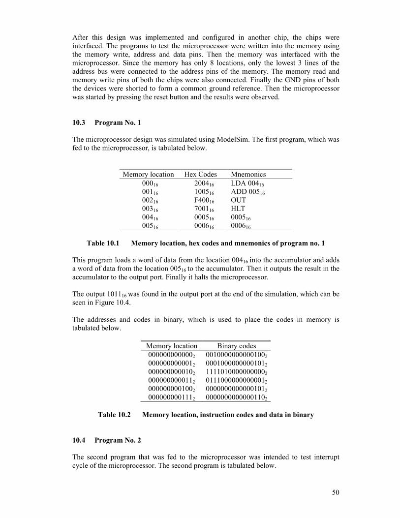
50
After this design was implemented and configured in another chip, the chips were
interfaced. The programs to test the microprocessor were written into the memory using
the memory write, address and data pins. Then the memory was interfaced with the
microprocessor. Since the memory has only 8 locations, only the lowest 3 lines of the
address bus were connected to the address pins of the memory. The memory read and
memory write pins of both the chips were also connected. Finally the GND pins of both
the devices were shorted to form a common ground reference. Then the microprocessor
was started by pressing the reset button and the results were observed.
10.3 Program No. 1
The microprocessor design was simulated using ModelSim. The first program, which was
fed to the microprocessor, is tabulated below.
Memory location Hex Codes Mnemonics
00016 200416 LDA 00416
00116 100516 ADD 00516
00216 F40016 OUT
00316 700116 HLT
00416 000516 000516
00516 000616 000616
Table 10.1 Memory location, hex codes and mnemonics of program no. 1
This program loads a word of data from the location 00416 into the accumulator and adds
a word of data from the location 00516 to the accumulator. Then it outputs the result in the
accumulator to the output port. Finally it halts the microprocessor.
The output 101116 was found in the output port at the end of the simulation, which can be
seen in Figure 10.4.
The addresses and codes in binary, which is used to place the codes in memory is
tabulated below.
Memory location Binary codes
0000000000002 00100000000001002
0000000000012 00010000000001012
0000000000102 11110100000000002
0000000000112 01110000000000012
0000000001002 00000000000001012
0000000001112 00000000000001102
Table 10.2 Memory location, instruction codes and data in binary
10.4 Program No. 2
The second program that was fed to the microprocessor was intended to test interrupt
cycle of the microprocessor. The second program is tabulated below.

51
Memory location Hex Codes Mnemonics
00016 400216 BUN 00216
00116 400416 BUN 00416
00216 F08016 ION
00316 400216 BUN 00216
00416 700116 HLT
Table 10.3 Memory location, hex codes and mnemonics of program no. 1
This program branches to address 00216 after the first instruction and enables the
interrupt. Then the control keeps moving in a loop unless an interrupt takes place. When
the intr_in pin is made high to interrupt the processor, the normal execution of the loop is
suspended and the instruction at location 00116 is executed. Thus it branches to location
00416 which is the instruction to halt the processor.
The addresses and codes in binary which is used to place the codes in memory is
tabulated below.
Memory location Hex Codes Mnemonics
00016 400216 BUN 00216
00116 400416 BUN 00416
00216 F08016 ION
00316 400216 BUN 00216
00416 700116 HLT
Table 10.4 Memory location, instruction codes and data in binary
10.5 Simulation Results of Programming of Memory
The programming of memory was simulated by ModelSim. The next two pages shows
snapshots of the simulation results obtained by ModelSim in Figure 10.2 and Figure 10.3.
Figure 10.2 shows the simulation of the programming of memory for program no. 1 and
Figure 10.3 shows the simulation of the programming of memory for program no. 2.
10.6 Simulation Results of Execution of Programs
The execution of the programs by the microprocessor was simulated by ModelSim. The
snapshots of the simulation are given in Figure 10.4 and Figure 10.5. Figure 10.4 is the
simulation result for program no. 1. Figure 10.5 is the simulation result for program no. 2.
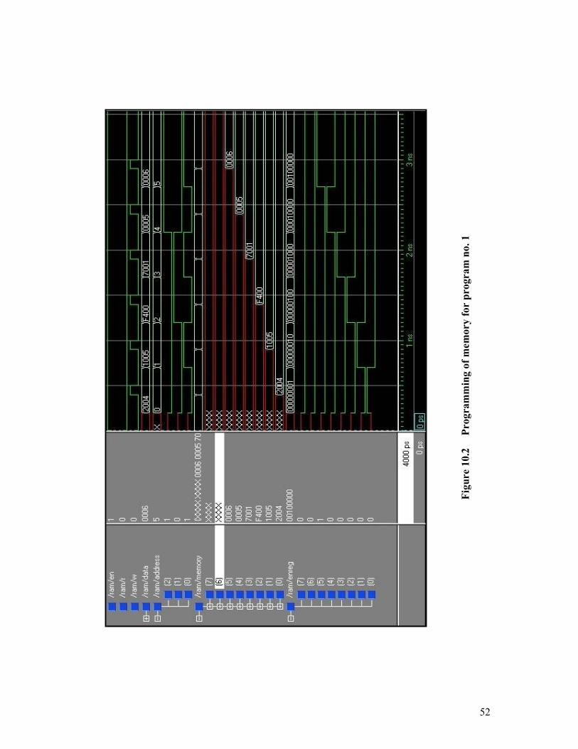
52
Figure 10.2 Programming of memory for program no. 1
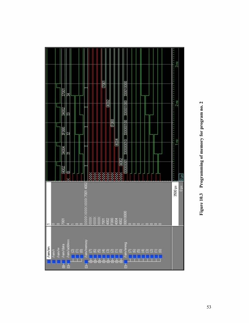
53
Figure 10.3 Programming of memory for program no. 2

54
Figure 10.4 Execution of program no. 1

55
Figure 10.5 Execution of program no. 2

56
Conclusion
The 16-bit microprocessor was designed and tested successfully. Each instruction was
also simulated and tested. The design is simple and easy to understand. The
microprocessor was designed with a view to accommodate the various features of
microprocessors rather than having a large instruction set. Thus the instruction set was
kept small, consisting 25 instructions only and the available time was better utilized in
adding extra features like interrupts and providing facilities for input and output.
Some of the attractive features of the microprocessor are the facility for subroutine calls
and interrupts. It has dedicated input port and output port to handle input and output. The
address lines and the data lines have not been multiplexed and therefore relieve the extra
burden of including circuitry to demultiplex them.
There is a lot of scope for improvement. Though the instruction set contains all the basic
instructions with the help of which all kinds of programs can be written but a lot more
useful and handy instructions can be added to make the life of programmer easier. A
major limitation is that only one input device and one output device can be connected to
the interrupt. The instruction for subroutine call doesn’t use the concept of stack to save
return address. A stack may be introduced which also makes storing data temporarily and
retrieving them easier. The number of processor registers should be increased. This will
lessen the use of memory reference instructions which needs more timing signals than
register reference instructions.
Though the microprocessor designed in this project is small compared to commercial
microprocessors, it has the advantage of being simple enough to demonstrate the design
process, design the processor and test its operation in the given time constraint and
configure it in the CPLD chip provided, which can hold a limited number of logic gates.

57
Bibliography
1. Computer System Architecture
Third Edition
By M. Morris Mano
Prentice-Hall India
2. Microprocessor Architecture, Programming and Applications with the 8085
Fourth Edition
By Ramesh S. Gaonkar
Penram International
3. VHDL Primer
Third Edition
By J. Bhasker
Prentice-Hall India


![Week 2 The 80x86 Microprocessor Architecturealkar/ELE414/dirz2005/w2-414-[2005].pdf · – 8086 is a microprocessor with a 16-bit data ... – All specification of the hardware and](https://img.dokumen.tips/doc/110x75/5aab6e387f8b9aa06a8be4b0/week-2-the-80x86-microprocessor-alkarele414dirz2005w2-414-2005pdf-8086.jpg)