Embed Size (px)
Citation preview

Mary Jo W. ShalkhauserGlenn Research Center, Cleveland, Ohio
Programmable Logic Device (PLD) DesignDescription for the Integrated Power, Avionics, and Software (iPAS) Space Telecommunications Radio System (STRS) Radio
NASA/TM—2017-219429
April 2017
https://ntrs.nasa.gov/search.jsp?R=20170004668 2018-06-03T11:15:30+00:00Z

NASA STI Program . . . in Profi le
Since its founding, NASA has been dedicated to the advancement of aeronautics and space science. The NASA Scientifi c and Technical Information (STI) Program plays a key part in helping NASA maintain this important role.
The NASA STI Program operates under the auspices of the Agency Chief Information Offi cer. It collects, organizes, provides for archiving, and disseminates NASA’s STI. The NASA STI Program provides access to the NASA Technical Report Server—Registered (NTRS Reg) and NASA Technical Report Server—Public (NTRS) thus providing one of the largest collections of aeronautical and space science STI in the world. Results are published in both non-NASA channels and by NASA in the NASA STI Report Series, which includes the following report types: • TECHNICAL PUBLICATION. Reports of
completed research or a major signifi cant phase of research that present the results of NASA programs and include extensive data or theoretical analysis. Includes compilations of signifi cant scientifi c and technical data and information deemed to be of continuing reference value. NASA counter-part of peer-reviewed formal professional papers, but has less stringent limitations on manuscript length and extent of graphic presentations.
• TECHNICAL MEMORANDUM. Scientifi c
and technical fi ndings that are preliminary or of specialized interest, e.g., “quick-release” reports, working papers, and bibliographies that contain minimal annotation. Does not contain extensive analysis.
• CONTRACTOR REPORT. Scientifi c and technical fi ndings by NASA-sponsored contractors and grantees.
• CONFERENCE PUBLICATION. Collected papers from scientifi c and technical conferences, symposia, seminars, or other meetings sponsored or co-sponsored by NASA.
• SPECIAL PUBLICATION. Scientifi c,
technical, or historical information from NASA programs, projects, and missions, often concerned with subjects having substantial public interest.
• TECHNICAL TRANSLATION. English-
language translations of foreign scientifi c and technical material pertinent to NASA’s mission.
For more information about the NASA STI program, see the following:
• Access the NASA STI program home page at http://www.sti.nasa.gov
• E-mail your question to [email protected] • Fax your question to the NASA STI
Information Desk at 757-864-6500
• Telephone the NASA STI Information Desk at 757-864-9658 • Write to:
NASA STI Program Mail Stop 148 NASA Langley Research Center Hampton, VA 23681-2199

Mary Jo W. ShalkhauserGlenn Research Center, Cleveland, Ohio
Programmable Logic Device (PLD) DesignDescription for the Integrated Power, Avionics, and Software (iPAS) Space Telecommunications Radio System (STRS) Radio
NASA/TM—2017-219429
April 2017
National Aeronautics andSpace Administration
Glenn Research CenterCleveland, Ohio 44135

Available from
Level of Review: This material has been technically reviewed by technical management.
NASA STI ProgramMail Stop 148NASA Langley Research CenterHampton, VA 23681-2199
National Technical Information Service5285 Port Royal RoadSpringfi eld, VA 22161
703-605-6000
This report is available in electronic form at http://www.sti.nasa.gov/ and http://ntrs.nasa.gov/
Trade names and trademarks are used in this report for identifi cation only. Their usage does not constitute an offi cial endorsement, either expressed or implied, by the National Aeronautics and
Space Administration.

NASA/TM—2017-219429 1
Programmable Logic Device (PLD) Design Description for the Integrated Power, Avionics, and Software (iPAS) Space
Telecommunications Radio System (STRS) Radio
Mary Jo W. Shalkhauser National Aeronautics and Space Administration
Glenn Research Center Cleveland, Ohio 44135
Summary
The Space Telecommunications Radio System (STRS) provides a common, consistent framework for software defined radios (SDRs) to abstract the application software from the radio platform hardware. The STRS standard aims to reduce the cost and risk of using complex, configurable, and reprogrammable radio systems across NASA missions. To promote the use of the STRS architecture for future NASA advanced exploration missions, NASA Glenn Research Center developed an STRS compliant SDR on a radio platform used by the Advanced Exploration System program at the Johnson Space Center in their Integrated Power, Avionics, and Software (iPAS) laboratory. At the conclusion of the development, the software and hardware description language (HDL) code was delivered to Johnson for their use in their iPAS testbed to get hands-on experience with the STRS standard, and for development of their own STRS waveforms on the now STRS-compliant platform.
1.0 Introduction
The Integrated Power, Avionics, and Software (iPAS) Space Telecommunications Radio System (STRS) radio was implemented on the Reconfigurable, Intelligently-Adaptive Communication System (RIACS) platform, currently being used for radio development at the NASA Johnson Space Center. The platform consists of a Xilinx® Virtex®-6 ML605 Evaluation Kit, an Analog Devices AD–FMCOMMS1–EBZ radiofrequency (RF) front-end board, and an Axiomtek™ eBOX620–110–FL embedded personal computer (PC) running the Ubuntu® 12.04 LTS operating system. Figure 1 shows the RIACS platform hardware. The result of this development is a very low cost, STRS-compliant platform that can be used for waveform developments for multiple applications. The purpose of this document is to describe the design of the hardware description language (HDL) code for the field-programmable gate array (FPGA) portion of the iPAS STRS radio, particularly the design of the FPGA wrapper and the test waveform.

NASA/TM—2017-219429 2
Figure 1.—Reconfigurable, Intelligently-Adaptive Communication System (RIACS) platform
components. ADC, analog-to-digital converter; DAC, digital-to-analog converter; FPGA, field-programmable gate array; RF, radiofrequency; Rx, receive; Tx, transmit.
2.0 Programmable Logic Device (PLD) Design Overview
This section provides an overview of the PLD design.
2.1 Purpose
The purpose of the programmable logic device (PLD) design is the implementation of the signal processing functions of the STRS radio architecture in the iPAS RIACS platform. The PLD design consists of two parts: the FPGA wrapper and the test waveform. The FPGA wrapper implements each of these platform interfaces:
(1) Ethernet communication to the embedded processor for commanding and data streaming (2) Digital-to-analog converter (DAC) and analog-to-digital converter (ADC) interface to the
radiofrequency (RF) board (3) RF board control and configuration (4) FPGA clocking
The test waveform does not fully implement all the signal processing functionality for a radio, but it
exercises and demonstrates each interface in the FPGA wrapper. A future user of the platform for an STRS radio would use the FPGA wrapper and replace the test waveform with their own radio signal processing functions.
The PLD design is required to receive and process commands and provide command control and data to the test waveform. It must also receive (Rx) and transmit (Tx) streaming data from and to the embedded processor. The test waveform demonstrates each FPGA wrapper interface. To test Tx-side streaming, it can perform bit error rate (BER) testing on Tx-side pseudorandom bit sequence (PRBS) streaming data. It can also generate PRBS streaming data packets for an Rx-side streaming data source. The test waveform generates sine waves for the in-phase (I) and quadrature (Q) inputs to the RF
NASA/TM—2017-219429 3
transceiver. A binary phase shift keying (BPSK) modulator is included to modulate data from the PRBS generator or from Tx-side streaming data. Captured I and Q samples from the RF transceiver can be streamed to the embedded processor where it can be plotted (if a sine wave) or BER checked (if PRBS data) to demonstrate proper functionality of the RF board and its interfaces. The Xilinx® ChipScope™ Pro tool can be used on the Rx side to view the data received from the ADC.
2.2 Top-Level Design Description
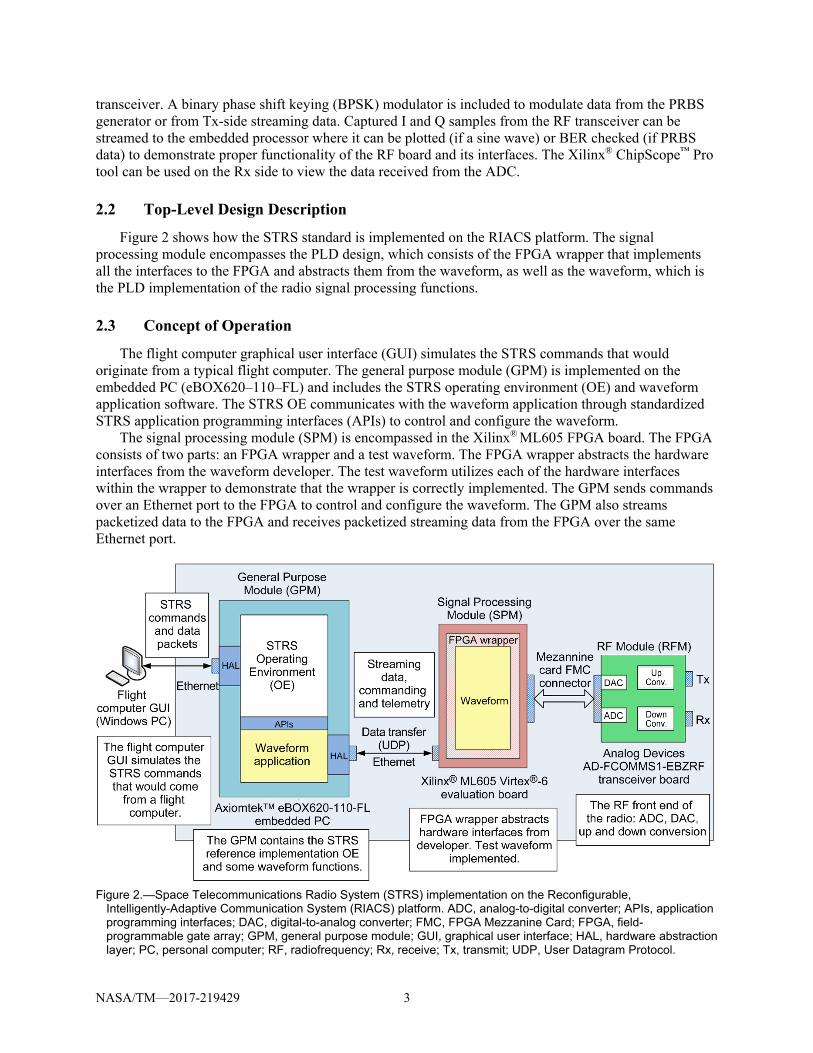
Figure 2 shows how the STRS standard is implemented on the RIACS platform. The signal processing module encompasses the PLD design, which consists of the FPGA wrapper that implements all the interfaces to the FPGA and abstracts them from the waveform, as well as the waveform, which is the PLD implementation of the radio signal processing functions.
2.3 Concept of Operation
The flight computer graphical user interface (GUI) simulates the STRS commands that would originate from a typical flight computer. The general purpose module (GPM) is implemented on the embedded PC (eBOX620–110–FL) and includes the STRS operating environment (OE) and waveform application software. The STRS OE communicates with the waveform application through standardized STRS application programming interfaces (APIs) to control and configure the waveform.
The signal processing module (SPM) is encompassed in the Xilinx® ML605 FPGA board. The FPGA consists of two parts: an FPGA wrapper and a test waveform. The FPGA wrapper abstracts the hardware interfaces from the waveform developer. The test waveform utilizes each of the hardware interfaces within the wrapper to demonstrate that the wrapper is correctly implemented. The GPM sends commands over an Ethernet port to the FPGA to control and configure the waveform. The GPM also streams packetized data to the FPGA and receives packetized streaming data from the FPGA over the same Ethernet port.
Figure 2.—Space Telecommunications Radio System (STRS) implementation on the Reconfigurable,
Intelligently-Adaptive Communication System (RIACS) platform. ADC, analog-to-digital converter; APIs, application programming interfaces; DAC, digital-to-analog converter; FMC, FPGA Mezzanine Card; FPGA, field-programmable gate array; GPM, general purpose module; GUI, graphical user interface; HAL, hardware abstraction layer; PC, personal computer; RF, radiofrequency; Rx, receive; Tx, transmit; UDP, User Datagram Protocol.

NASA/TM—2017-219429 4
The RF front-end board (AD–FMCOMMS1–EBZ) contains a DAC, up-converter, down-converter, and an ADC. The FPGA configures the RF board using the embedded Xilinx® MicroBlaze™ 32-bit Reduced Instruction Set Computer soft processor and sends I and Q data to the DAC converter. The FPGA also receives down-converted and sampled I and Q data from ADC on the RF board.
The test waveform will be able to demonstrate STRS commands for configuration and control of the test waveform, Tx-side streaming data operation, RF front-end board configuration, Rx-side streaming data, and STRS telemetry querying.
2.4 Design Decisions
The RF front-end board (AD–FMCOMMS1–EBZ) comes with a reference design to aid developers in using the board. The reference design, implemented using the Xilinx® Embedded Development Kit (EDK) and Software Development Kit (SDK) tools, is complex and contains functionality not necessary for the STRS radio implementation. It was decided to use the reference design only for the configuration of the RF board and not for the data paths. The FPGA wrapper will, therefore, be able to interface directly to the DAC and ADC through VHSIC Hardware Development Language (VHDL) in the Xilinx® Integrated Synthesis Environment (ISE) Project Navigator. This approach greatly simplifies the FPGA wrapper and the insertion of new waveforms.
The test waveform includes a BPSK modulator to provide a better demonstration of the RF module (RFM). PRBS data is modulated when data is transmitted through the RFM. The modulated data into the DAC and out of the ADC is viewable using the Xilinx® ChipScope™ Pro tool, but the signal out of the ADC is not demodulated in this implementation.
It was decided early in the development phase to use the single Ethernet port on the Xilinx® ML605 FPGA board for command and streaming data. This was done because it required only one interface to be implemented. Since command packets are short and relatively infrequent, they are unlikely to interfere with streaming data packets.
The command packet length was defined to be 49 total bytes. Command responses are 60 bytes in length. Streaming data packets are 557 total bytes. In each case, 42 bytes are Ethernet header bytes that consist of the media access control (MAC) header (14 bytes), Internet Protocol (IP) header (20 bytes), and User Datagram Protocol (UDP) header (8 bytes). The total length of the packets (i.e., the payload portion of each packet) can be changed to accommodate new designs simply by changing the appropriate constants in STRS_Radio_Pkg.vhd.
The GPM processor (eBOX620–110–FL) transmits and receives command and response packets over a UDP port number that is separate from the UDP port used for streaming data. Table 1 shows the port numbers that were selected for each type of packet.
Status bits are created throughout the FPGA wrapper and test waveform to provide an indication of problems while the FPGA is operating. These status bits include first in first out (FIFO) underflow and overflow flags, error flags for every state machine in case any state machine navigates to an erroneous state, bit error rate tester (BERT) sync lost and sync loss count flags, and a few other error flags. The status bits are sent to the GPM processor in a response to a status bits query command. Details of the status bits are contained throughout Section 4.0. The status bits are defined in Table 26 in Section 4.2.
TABLE 1.—USER DATAGRAM PROTOCOL (UDP) PORT ADDRESSES Port definition Hex value Decimal
value FPGAa port address for commands and response packets 0xD6D8 55,000 FPGA port address for streaming data packets 0xDAC0 56,000 Linux PCb port address for commands and response packets 0x8C35 35,893 Linux PC port address for streaming data packets 0x8CA0 36,000
aField-programmable gate array. bPersonal computer.

NASA/TM—2017-219429 5
3.0 Programmable Logic Device (PLD) Architectural Design Description
This section provides a description of the architectural design of the PLD.
3.1 Hardware Identification
This PLD design is implemented on a Xilinx® ML605 Rev D evaluation board, which contains a Xilinx® Virtex®-6 XC6VLX240T-1FF1156C FPGA. The AD–FMCOMMS1–EBZ RF front-end board is used for the RF front end.
3.2 Development Tools
The development tool used for this PLD design is the Xilinx® ISE Design Suite System Edition version 14.4, which includes EDK and SDK.
3.3 Programmable Logic Device (PLD) Overall Architecture
Figure 3 contains a high-level block diagram of the PLD design. The FPGA wrapper in an STRS radio is platform specific, abstracts all interfaces away from the waveform, and contains any functionality needed by all waveforms using the platform. Figure 3 shows the basic functionality in both the wrapper and the waveform. The FPGA wrapper includes the logic and physical interfaces required for clock generation, reset signal generation, and Ethernet control and processing. Ethernet processing includes the following:
(1) Stripping off of Ethernet headers (2) Routing of received command packets and Tx-side streaming data packets (3) Creation of packets for command responses and Rx-side streaming data (4) Control of the sequence of the transmission of command response and Rx-side streaming
data packets
The wrapper also includes the MicroBlaze™ processor implementation of the Inter-Integrated Circuit (IIC) bus interface to the RFM for configuration purposes.
A test waveform, called waveform in Figure 3, is included in the PLD design to exercise and demonstrate each of the FPGA wrapper interfaces. This test waveform receives command packets and parses them to configure and control the waveform. Four data sources are included to provide data to the RFM or for testing and demonstrating the functionality of the radio platform and the wrapper interfaces. The waveform also includes three possible data sinks for demonstrating the platform and wrapper.
3.4 Detailed Architecture Design and Block Diagrams
Figure 4 contains a detailed block diagram of the Tx side of the PLD design. Most of the blocks in the diagram (and subsequent block diagrams) represent HDL code modules and are labeled with the module or instance name, so that these functions can be easily located in the code. Some blocks may contain submodules that will be described in Section 4.0. This block diagram shows Tx-side wrapper functions, which include clock generation, reset signal generation, and the modules to receive streaming and command packets and remove Ethernet headers. The block diagram also shows the Tx-side waveform functions, which include command parsing and decoding, conversion of streaming packet data into continuous streaming data, PRBS generation, and I and Q signal generation (sine waves).

NASA/TM—2017-219429 6
Figure 3.—Programmable logic device (PLD) design. BERT, bit error rate tester; BPSK, binary phase shift key; IIC,
Inter-Integrated Circuit; MUX, multiplexer; PHY, physical layer; PRBS, pseudorandom bit sequence; Rx, receive; Tx, transmit.
Figure 4.—Transmit-side wrapper and waveform. EMAC, Ethernet Media Access Controller; LEDs, light-emitting
diodes.

NASA/TM—2017-219429 7
Figure 5.—Receive-side wrapper and waveform. ADC, analog-to-digital converter; BERT, bit error rate tester; EMAC,
Ethernet Media Access Controller; MUX, multiplexer; PRBS, pseudorandom bit sequence; Rx, receive; Tx, transmit.
Figure 5 contains the detailed block diagram of the Rx side of the PLD design. The Rx-side waveform performs BER testing of PRBS or streaming data. The Rx-side wrapper packetizes command responses, Rx-side streaming data, and controls their transmission over the Ethernet port.
3.5 Ethernet Packet Structure
Figure 6 shows the definition of the Ethernet header (MAC header, IP datagram header, and UDP header).
When packets are sent from the FPGA to the GPM processor, the packet headers must be inserted when the packets are formed. In each case, the headers are created at design time and stored in ROMs to be read out and inserted in the packets. The UDP checksum field is optional and is set to zero for all packets created by the FPGA. The IP datagram header checksum must be calculated, however. This calculation includes only bytes in the IP datagram (i.e., not the MAC header or the UDP datagram).
Here are the steps for calculating the IP datagram header checksum field: (1) Add up the values of the 16-bit words in the IP datagram, excluding the checksum field. (2) Any binary digits above bit 15 (the carry bits) should be added to bits 0 to 15 of the sum above. (3) Invert the result to get the checksum.

NASA/TM—2017-219429 8
Example IP header:
4500 002E 0000 4000 4011 XXXX C0A8 0002 COA8 0001 (where XXXX is the checksum)
The sum of each word is: 0x24692
0x24692 10 | 0100 0110 1001 0010 Add the carry bits + 10
Sum 0100 0110 1001 0100 Invert 1011 1001 0110 1011 = 0xB96B = checksum
MAC header MAC destination address (6 bytes) MAC source address (6 bytes) Ethernet type
(2 bytes)
IP datagram
Version (4 bits)
IHL (4 bits)
Type of service (8 bits)
Length (IP + UDP + payload, 2 bytes)
Identification (2 bytes) Flags (3 bits) Fragment offset (13 bits)
Time to live (1 byte)
Protocol (1 byte)
IP header checksum (2 bytes)
Source IP address (4 bytes) Destination IP address (4 bytes) UDP header Source port (2 bytes) Destination port (2 bytes)
Length (UDP + payload, 2 bytes) UDP checksum (2 bytes)
Payload Various Lengths
Figure 6.—Ethernet packet definition. IHL, Internet header length; IP, Internet Protocol; MAC, media access control; UDP, User Datagram Protocol.
3.6 MicroBlaze™ Processor
The MicroBlaze™ processor core is used for the Xilinx® Virtex®-6 FPGA that is used in the iPAS radio design to configure the front-end board (AD–FMCOMMS1–EBZ). Analog Devices provides a reference design to help use their RF front-end board (AD–FMCOMMS1–EBZ) with the Xilinx® ML605 FPGA board. The reference design is available through their online Wiki at https://wiki.analog.com/resources/eval/user-guides/ad-fmcomms1-ebz
The reference design contains functionality that was not needed for the iPAS STRS radio, so that functionality was removed from the MicroBlaze.xmp (Xilinx® Platform Studio) portion of the reference design, leaving only the functionality necessary to configure and provide clocking to the RF board and the universal asynchronous receiver/transmitter (UART). This allows the waveform developer the ability to connect to the RF Board’s DAC and ADC directly using VHDL.
The SDK portion of the reference design SDK was retained in the iPAS STRS radio. The main.c was edited to configure the ADC sampling rate (196.608 MHz), the DAC sampling rate (196.608 MHz), and the Rx RF gain (+10 dB). The default SDK configuration is provided in the CompiledDefaultProgram.elf file.
The MicroBlaze™ processor uses a UART peripheral to display the configuration of the RF front-end board (AD–FMCOMMS1–EBZ). When the MicroBlaze™ processor starts after a power-on or reset, the UART will send the following information to a terminal—ADC and DAC sampling rates, variable-gain amplifier (VGA) gain, and Rx and Tx RF frequency. The UART configuration necessary for the PC-based receiver is—57,600 baud, 8-bit data, no parity bit, 1 stop bit, and no flow control. Use of the UART requires the installation of a driver on the PC.
3.7 External Interfaces
External interfaces are described in the Hardware Interface Description (HID) iPAS STRS Radio document (Ref. 1).

NASA/TM—2017-219429 9
4.0 Programmable Logic Device (PLD) Detailed Design
Each of the modules in the PLD is described in detail below. Note that color coding on block diagrams is used to show each clock domain. Light orange indicates the 125 MHz clock domain and light blue indicates the waveform clock domain. Throughout this section, VHDL signal names are always shown in italics and file names are shown in a monospaced, typewriter style Courier font. VHDL constants are always shown in all capital letters.
4.1 STRS_SDR_Wrapper.vhd
The STRS_SDR_Wrapper module is the top-level module in the PLD design. STRS requires that the FPGA wrapper for an STRS radio encompass all the possible radio FPGA interfaces. The wrapper abstracts the interfaces to the FPGA from the waveform. The wrapper can also include any other functionality that a radio would require, like power-on resets and clock generation, which would be common to all radios on the platform.
The STRS_SDR_Wrapper module is the FPGA wrapper, and therefore contains the clock generation and reset creation. This wrapper also has interfaces to onboard resources like switches and light-emitting diodes (LEDs), as well as the implementation of the interface to the Ethernet physical layer (PHY) for receiving commands and streaming data from the GPM processor and for transmitting command responses and streaming data to the processor. The wrapper also contains the interface to the RF front-end board.
The STRS_SDR_Wrapper module utilizes a Xilinx® LogiCORE™ IP Clocking Wizard to generate the clocks necessary for the wrapper and the test waveform. The source input clock (200 MHz) for the clock wizard is single-ended and is generated by the MicroBlaze™ processor from the 200 MHz differential clock from a crystal on the Xilinx® ML605 FPGA board. The clock wizard creates the following clocks:
RefClk—200 MHz clock used by the Ethernet IP core. GtxClk—125 MHz single-ended clock which is used by the Ethernet interface. The waveform clocks originate in the DAC device on the RFM for the Tx side and the ADC device
on the RFM for the Rx side. These DAC and ADC clocks (approximately 196.6 MHz) are used in the wrapper to generate clock enable signals to control clocking within the waveform.
In addition to the generation of the clocks and resets, the wrapper instantiates the Ethernet Media Access Controller (EMAC) interface (v6_emac_v1_5_example_design.vhd) and the radio test waveform (STRS_Waveform.vhd). The wrapper also includes the modules that provide the basic functionality to communicate in both directions to the Ethernet interface. These modules include EthernetRx and RxPackets for receiving and parsing Tx-side streaming data packets and command packets, as well as OutputDataMux for transmitting Rx-side streaming and command response packets. Each of these modules are discussed in detail below.
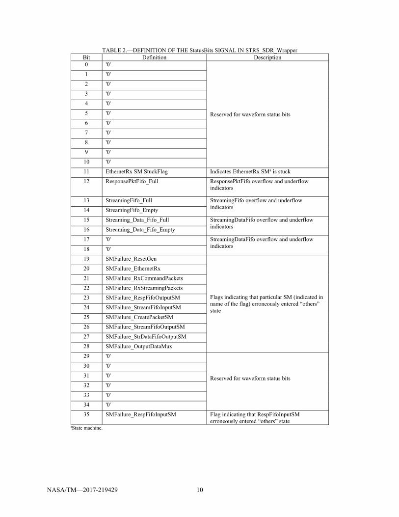
The ErrorFlag process, in the wrapper, registers and combines the error flags generated from the wrapper submodules into a word called StatusBits that is used as an input to the waveform module. This allows the status bits from the wrapper to be sent in response to a status request command. Table 2 shows the bit definition of the StatusBits signal in the STRS_SDR_Wrapper module. Table 3 shows the STRS_SDR_Wrapper module inputs and outputs.
NASA/TM—2017-219429 10
TABLE 2.—DEFINITION OF THE StatusBits SIGNAL IN STRS_SDR_Wrapper Bit Definition Description 0 '0'
Reserved for waveform status bits
1 '0'
2 '0'
3 '0'
4 '0'
5 '0'
6 '0'
7 '0'
8 '0'
9 '0'
10 '0'
11 EthernetRx SM StuckFlag Indicates EthernetRx SMa is stuck
12 ResponsePktFifo_Full ResponsePktFifo overflow and underflow indicators
13 StreamingFifo_Full StreamingFifo overflow and underflow indicators 14 StreamingFifo_Empty
15 Streaming_Data_Fifo_Full StreamingDataFifo overflow and underflow indicators 16 Streaming_Data_Fifo_Empty
17 '0' StreamingDataFifo overflow and underflow indicators 18 '0'
19 SMFailure_ResetGen
Flags indicating that particular SM (indicated in name of the flag) erroneously entered “others” state
20 SMFailure_EthernetRx
21 SMFailure_RxCommandPackets
22 SMFailure_RxStreamingPackets
23 SMFailure_RespFifoOutputSM
24 SMFailure_StreamFifoInputSM
25 SMFailure_CreatePacketSM
26 SMFailure_StreamFifoOutputSM
27 SMFailure_StrDataFifoOutputSM
28 SMFailure_OutputDataMux
29 '0'
Reserved for waveform status bits
30 '0'
31 '0'
32 '0'
33 '0'
34 '0'
35 SMFailure_RespFifoInputSM Flag indicating that RespFifoInputSM erroneously entered “others” state
aState machine.

NASA/TM—2017-219429 11
TABLE 3.—STRS_SDR_Wrapper INPUTS AND OUTPUTS Module inputs
CLK_N Differential FPGAa system clock (200 MHz)—negative CLK_P Differential FPGA system clock (200 MHz)—positive USER_CLOCK FPGA user clock (66 MHz) GMII_RXD Ethernet receive data (8 bits, from PHYb) GMII_RX_DV Ethernet receive data valid (from PHY) GMII_RX_ER Ethernet receive error (from PHY) GMII_RX_CLK Ethernet receive clock (from PHY) RESET Reset signal from push button on FPGA board GPIO_DIP_SW1 Dip switch 1 on FPGA board GPIO_DIP_SW2 Dip switch 2 on FPGA board GPIO_DIP_SW3 Dip switch 3 on FPGA board GPIO_DIP_SW4 Dip switch 4 on FPGA board GPIO_DIP_SW5 Dip switch 5 on FPGA board GPIO_DIP_SW6 Dip switch 6 on FPGA board GPIO_DIP_SW7 Dip switch 7 on FPGA board GPIO_DIP_SW8 Dip switch 8 on FPGA board DacClkInP 196.6 MHz clock from DACc (p) DacClkInN 196.6 MHz clock from DAC (n) UartRx UARTd receive data AdcClkInP 196.6 MHz clock from ADC; synchronous with ADC data (p) AdcClkInN 196.6 MHz clock from ADC; synchronous with ADC data (n) AdcOrInP Differential overrange indicator, positive (not used) AdcOrInN Differential overrange indicator, negative (not used) AdcDataInP ADCe data in (14 bits)—positive AdcDataInN ADC data in (14 bits)—negative
Module outputs GMII_TXD Ethernet transmit data (8 bits, to PHY) GMII_TX_EN Ethernet transmit enable (to PHY) GMII_TX_ER Ethernet transmit error (to PHY) GMII_TX_CLK Ethernet transmit clock (to PHY) PHY_RESET Reset signal to the Ethernet PHY chip GPIO_LED_0 LEDf 0 on FPGA board GPIO_LED_1 LED 1 on FPGA board GPIO_LED_2 LED 2 on FPGA board GPIO_LED_3 LED 3 on FPGA board GPIO_LED_4 LED 4 on FPGA board GPIO_LED_5 LED 5 on FPGA board GPIO_LED_6 LED 6 on FPGA board GPIO_LED_7 LED 7 on FPGA board DacClkOutP 196.6 MHz clock to DAC; synchronous with DAC data (p) DacClkOutN 196.6 MHz clock to DAC; synchronous with DAC data (n) DacFrameOutP Differential frame output (p) DacFrameOutN Differential frame output (n) DacDataOutP 16-bit DAC output data—positive DacDataOutN 16-bit DAC output data—negative RefClkP 30 MHz reference clock for RF board (positive) RefClkN 30 MHz reference clock for RF board (negative) UartTx UART transmit data
Module in/outs IicSda IICg bus serial data line IicScl IIC bus serial clock line
aField-programmable gate array. bPhysical layer. cDigital-to-analog converter. dUniversal asynchronous receiver/transmitter. eAnalog-to-digital converter. fLight-emitting diode. gInter-Integrated Circuit.

NASA/TM—2017-219429 12
4.1.1 ResetGen.vhd
The ResetGen module creates the SystemReset signal, which is the system reset signal for the entire STRS radio FPGA design. The SystemReset signal will be asserted (high) when the board first powers on, when the reset push button is pushed, and when a reset command is received (creating the signal called SoftReset). When the FPGA board is first powered on, the phase-locked loop (PLL) in ClockWizard66 is not locked. When the PLL locks, the Locked signal goes high, which enables the ResetGen finite state machine. The ResetGen module is clocked by Clock66, the 66 MHz clock output from the ClockWizard66.
A state machine in the ResetGen module controls the generation of the SystemReset signal. At startup, the state machine first waits for the ClockWizard66 Locked signal, which is connected to the Enable input signal, to go high. At this point the state machine goes into the WAITING state to wait for a counter to count up to the value of WAIT_COUNT (currently 100). This wait state is to make sure the MicroBlaze™ processor has had enough time to initialize. The state machine then jumps to the POR state where the SystemReset signal is asserted high for a count length equal to FINAL_COUNT (currently 40). The state machine will then navigate to the READY state to await either a push button reset or a SoftReset from a reset command, both of which will cause the state machine to jump to the POR state and issue a SystemReset. If the Locked signal goes low while in any state, the state machine will jump to the IDLE state.
The state machine diagram for the ResetGen module is shown in Figure 7. Table 4 shows the inputs and outputs of the ResetGen module. The outputs of the state machine are as follows:
(1) RCountEn, which is used to start the reset length counter in the POR state. (2) WCountEn, which is used to start the wait length counter in the WAITING state. (3) ResetO, which is reassigned to become the output signal called SystemReset.
Figure 7.—ResetGen state machine.
NASA/TM—2017-219429 13
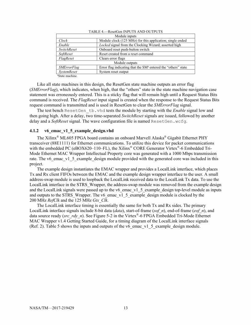
TABLE 4.—ResetGen INPUTS AND OUTPUTS Module inputs
Clock Module clock (125 MHz) for this application; single ended Enable Locked signal from the Clocking Wizard; asserted high SwitchReset Onboard reset push-button switch SoftReset Reset created from a reset command FlagReset Clears error flags
Module outputs SMErrorFlag Error flag indicating that the SMa entered the “others” state SystemReset System reset output
aState machine.
Like all state machines in this design, the ResetGen state machine outputs an error flag (SMErrorFlag), which indicates, when high, that the “others” state in the state machine navigation case statement was erroneously entered. This is a sticky flag that will remain high until a Request Status Bits command is received. The FlagReset input signal is created when the response to the Request Status Bits request command is transmitted and is used in ResetGen to clear the SMErrorFlag signal.
The test bench ResetGen_tb.vhd tests the module by starting with the Enable signal low and then going high. After a delay, two time-separated SwitchReset signals are issued, followed by another delay and a SoftReset signal. The wave configuration file is named ResetGen.wcfg.
4.1.2 v6_emac_v1_5_example_design.vhd
The Xilinx® ML605 FPGA board contains an onboard Marvell Alaska® Gigabit Ethernet PHY transceiver (88E1111) for Ethernet communications. To utilize this device for packet communications with the embedded PC (eBOX620–110–FL), the Xilinx® CORE Generator Virtex®-6 Embedded Tri-Mode Ethernet MAC Wrapper Intellectual Property core was generated with a 1000 Mbps transmission rate. The v6_emac_v1_5_example_design module provided with the generated core was included in this project.
The example design instantiates the EMAC wrapper and provides a LocalLink interface, which places Tx and Rx client FIFOs between the EMAC and the example design wrapper interface to the user. A small address-swap module is used to loopback the LocalLink received data to the LocalLink Tx data. To use the LocalLink interface in the STRS_Wrapper, the address-swap module was removed from the example design and the LocalLink signals were passed up to the v6_emac_v1_5_example_design top-level module as inputs and outputs to the STRS_Wrapper. The v6_emac_v1_5_example_design module is clocked by the 200 MHz RefClk and the 125 MHz Gtx_Clk.
The LocalLink interface timing is essentially the same for both Tx and Rx sides. The primary LocalLink interface signals include 8-bit data (data), start-of-frame (sof_n), end-of-frame (eof_n), and data source ready (src_rdy_n). See Figure 5-2 in the Virtex®-6 FPGA Embedded Tri-Mode Ethernet MAC Wrapper v1.4 Getting Started Guide, for a timing diagram of the LocalLink interface signals (Ref. 2). Table 5 shows the inputs and outputs of the v6_emac_v1_5_example_design module.

NASA/TM—2017-219429 14
TABLE 5.—v6_emac_v1_5_example_design INPUTS AND OUTPUTS Client receiver interface
EMACCLIENTRXDVLD Output, receive data valid (not used) EMACCLIENTRXFRAMEDROP Output, frame dropped signal (not used) EMACCLIENTRXSTATS 6-bit output, Rxa statistics data (not used) EMACCLIENTRXSTATSVLD Output, asserted when the Rx statistics data is valid (not used) EMACCLIENTRXSTATSBYTEVLD Output, asserted if an Ethernet MACb frame byte is received (not used)
Client transmitter interface CLIENTEMACTXIFGDELAY 8-bit output, configurable interframe gap adjustment EMACCLIENTTXSTATS Output, Txc statistics data (not used) EMACCLIENTTXSTATSVLD EMACCLIENTTXSTATSVLD Output, asserted when Tx statistics data valid (not used) EMACCLIENTTXSTATSBYTEVLD Output, asserted if an Ethernet MAC frame byte is transmitted (not used)
MAC control interface CLIENTEMACPAUSEREQ Input CLIENTEMACPAUSEVAL 16-bit input
Clock signal GTX_CLK Input, 125 MHz clock
GMIId physical interface GMII_TXD 8-bit output, transmit data GMII_TX_EN Output, transmit enable GMII_TX_ER Output, transmit error GMII_TX_CLK Output, transmit clock GMII_RXD 8-bit input, receive data GMII_RX_DV Input, receive data valid GMII_RX_ER Input, receive error GMII_RX_CLK Input, receive clock
Reference clock for IODELAYs REFCLK Input, 200 MHz clock
Asynchronous reset RESET Input, reset
LocalLink interface clocking signal ll_clk_o Output, LocalLink clock (not used)
LocalLink interface transmitter connections tx_ll_data_o 8-bit input, transmit LocalLink data tx_ll_sof_n_o Input, transmit start-of-frame tx_ll_eof_n_o Input, transmit end-of-frame tx_ll_src_rdy_n_o Input, transmit source ready tx_ll_dst_rdy_n_o Output, transmit destination ready
LocalLink interface receiver connections rx_ll_data_o 8-bit output, receive LocalLink data rx_ll_sof_n_o Output, receive start-of-frame rx_ll_eof_n_o Output, receive end-of-frame rx_ll_src_rdy_n_o Output, receive source ready rx_ll_dst_rdy_n_o Output, receive destination ready
aReceive. bMedia access control. cTransmit. dGigabit Media Independent Interface.

NASA/TM—2017-219429 15
Figure 8.—EthernetRx module.
4.1.3 EthernetRx.vhd
The EthernetRx module (Fig. 8) receives data and control signals from the EMAC and looks at the source port value in the packet header to see if the packet is a command or streaming data. Enable signals to RxCommandPackets (CommandEn) and to RxStreamPackets (StrDataEn) are created based upon the source port value contained in the incoming packet.
The state machine (diagram shown in Fig. 9) in the EthernetRx module is used to determine if an incoming packet is a command or streaming data. The source port number in the incoming packet is used to determine the type of received packet while in states GET_SRC_ADDR1 and GET_SRC_ADDR2. If the source port number indicates a command packet, the state machine goes to branch with state EN_CMD_PARSE where CommandEn is set high. If the source port number indicates a streaming packet, the state machine goes to branch with state EN_STREAM_DATA where StrDataEn is set high. The state machine exits to IDLE at the end of the packet, when EthDataEof goes low. If the EthDataEof signal fails to go low when expected, the state machine navigates to the ERROR state, where an error flag is set.
The EthernetRx module is clocked by a 125 MHz clock (GtxClk). The EthernetRx module handles errors in one of three ways: (1) A sticky flag called SMErrorFlag is created if an error occurs, causing the state machine to enter
the “others” state in the state machine navigation case statement. (2) The state machine contains an ERROR state that is entered if the EthDataSrcRdy signal fails to
go high at the expected end of a command or streaming data packet. This is done to prevent the state machine from getting stuck in a state (either EN_CMD_PARSE or EN_STREAM_DATA) with no way to exit. If this ERROR state is entered, the StuckFlag is set high.
(3) Flags are created if the FIFO overflows (FifoFlag(0)) or underflows (FifoFlag(1)). All of these flags are sticky and are only cleared when the FlagReset signal is asserted.
Table 6 shows the inputs and outputs of the EthernetRx module. The test bench for this module is EthernetRx_tb.vhd. This test bench simulates incoming
packets by reading data from a text file called RxSourceData.txt. The wave configuration file is EthernetRx.wcfg.

NASA/TM—2017-219429 16
Figure 9.—EthernetRx state machine.
TABLE 6.—EthernetRx INPUTS AND OUTPUTS StreamPktByte1 Streaming source port byte MSBa (0x8C) StreamPktByte2 Streaming source port byte LSBb (0xA0) CmdPktByte1 Command source port byte MSB (0x8C) CmdPktByte2 Command source port byte LSB (0x35)
Module inputs Clock 125 MHz clock Reset Reset EthDataSrcRdy Ethernet data source ready—low when data is valid EthDataIn Ethernet data in (8-bits) EthDataSof Ethernet data start-of-frame EthDataEof Ethernet data end-of-frame FlagReset Resets sticky error flags
Module outputs SMErrorFlag Indicates that the SMc entered the “others” state ErrorFlag Indicates SM was stuck in state 5 or 8 EthDataOut Ethernet data out (8 bits) EthRdyOut Ethernet data source ready out (low when EthDataOut is valid) CommandEn Enable command parsing StrDataEn Enable streaming data
NASA/TM—2017-219429 17
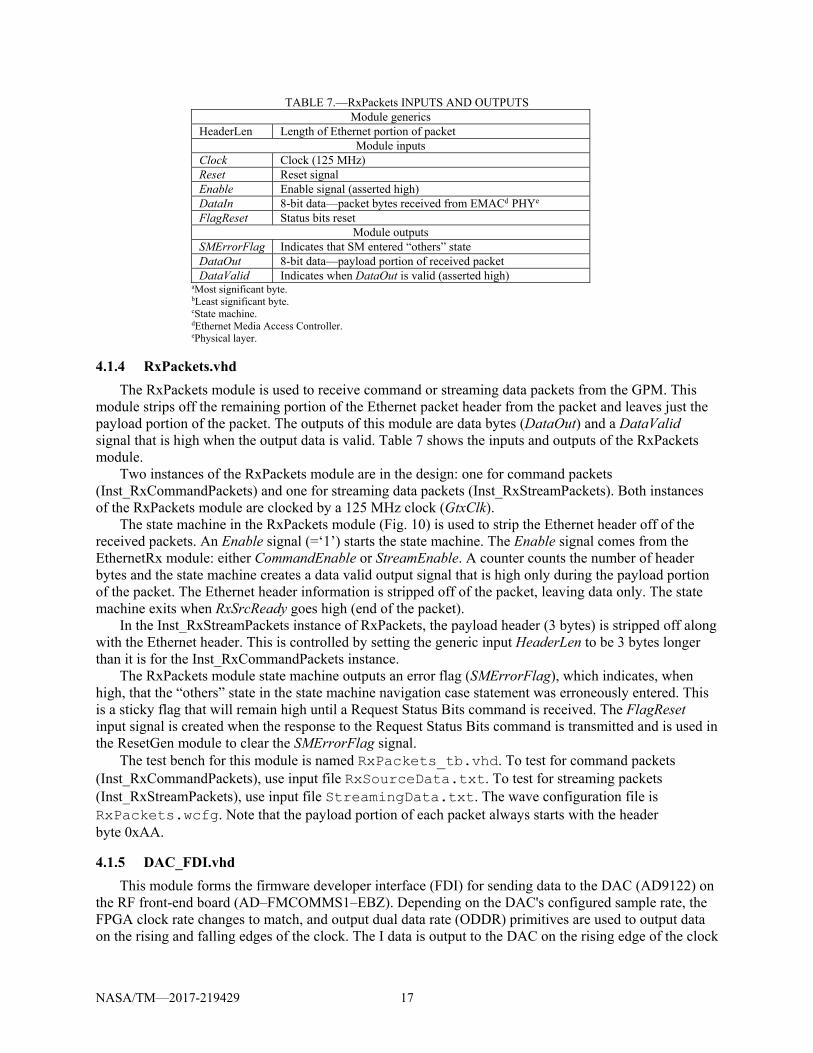
TABLE 7.—RxPackets INPUTS AND OUTPUTS Module generics
HeaderLen Length of Ethernet portion of packet Module inputs
Clock Clock (125 MHz) Reset Reset signal Enable Enable signal (asserted high) DataIn 8-bit data—packet bytes received from EMACd PHYe FlagReset Status bits reset
Module outputs SMErrorFlag Indicates that SM entered “others” state DataOut 8-bit data—payload portion of received packet DataValid Indicates when DataOut is valid (asserted high)
aMost significant byte. bLeast significant byte. cState machine. dEthernet Media Access Controller. ePhysical layer.
4.1.4 RxPackets.vhd
The RxPackets module is used to receive command or streaming data packets from the GPM. This module strips off the remaining portion of the Ethernet packet header from the packet and leaves just the payload portion of the packet. The outputs of this module are data bytes (DataOut) and a DataValid signal that is high when the output data is valid. Table 7 shows the inputs and outputs of the RxPackets module.
Two instances of the RxPackets module are in the design: one for command packets (Inst_RxCommandPackets) and one for streaming data packets (Inst_RxStreamPackets). Both instances of the RxPackets module are clocked by a 125 MHz clock (GtxClk).
The state machine in the RxPackets module (Fig. 10) is used to strip the Ethernet header off of the received packets. An Enable signal (=‘1’) starts the state machine. The Enable signal comes from the EthernetRx module: either CommandEnable or StreamEnable. A counter counts the number of header bytes and the state machine creates a data valid output signal that is high only during the payload portion of the packet. The Ethernet header information is stripped off of the packet, leaving data only. The state machine exits when RxSrcReady goes high (end of the packet).
In the Inst_RxStreamPackets instance of RxPackets, the payload header (3 bytes) is stripped off along with the Ethernet header. This is controlled by setting the generic input HeaderLen to be 3 bytes longer than it is for the Inst_RxCommandPackets instance.
The RxPackets module state machine outputs an error flag (SMErrorFlag), which indicates, when high, that the “others” state in the state machine navigation case statement was erroneously entered. This is a sticky flag that will remain high until a Request Status Bits command is received. The FlagReset input signal is created when the response to the Request Status Bits command is transmitted and is used in the ResetGen module to clear the SMErrorFlag signal.
The test bench for this module is named RxPackets_tb.vhd. To test for command packets (Inst_RxCommandPackets), use input file RxSourceData.txt. To test for streaming packets (Inst_RxStreamPackets), use input file StreamingData.txt. The wave configuration file is RxPackets.wcfg. Note that the payload portion of each packet always starts with the header byte 0xAA.
4.1.5 DAC_FDI.vhd
This module forms the firmware developer interface (FDI) for sending data to the DAC (AD9122) on the RF front-end board (AD–FMCOMMS1–EBZ). Depending on the DAC's configured sample rate, the FPGA clock rate changes to match, and output dual data rate (ODDR) primitives are used to output data on the rising and falling edges of the clock. The I data is output to the DAC on the rising edge of the clock

NASA/TM—2017-219429 18
and the Q data is output on the falling edge of the clock. Table 8 shows the inputs and outputs of the DAC_FDI module.
Figure 10.—RxPackets state machine.
TABLE 8.—DAC_FDI INPUTS AND OUTPUTS Module inputs
DacClkInP Differential clock input (P) DacClkInN Differential clock input (N) Clk200Mhz 200 MHz clock for IDELAY primitive Reset Asynchronous reset IncomingSamplesI Incoming Ia samples in two's complement IncomingSamplesQ Incoming Qb samples in two's complement
Module outputs ClkFromDAC Clock intended to drive incoming samples DacClkOutP Differential clock output (P) DacClkOutN Differential clock output (N) DacFrameOutP Differential frame output (P) DacFrameOutN Differential frame output (N) DacDataOutP Differential data output (P) DacDataOutN Differential data output (N)
aIn-phase. bQuadrature.

NASA/TM—2017-219429 19
TABLE 9.—ADC_FDI INPUTS AND OUTPUTS Module inputs
AdcClkInP Differential clock input (P) AdcClkInN Differential clock input (N) Clk200Mhz 200 MHz clock for IDELAY primitive Reset Asynchronous reset AdcOrInP Differential overrange indicator (P), not used AdcOrInN Differential overrange indicator (N), not used AdcDataInP Differential data input (P) AdcDataInN Differential data input (N)
Module outputs ClkFromADC Synchronous clock for outgoing samples OutgoingSamplesI Outgoing Ia samples in two’s complement OutgoingSamplesQ Outgoing Qb samples in two’s complement
aIn-phase. bQuadrature.
4.1.6 ADC_FDI.vhd
This module forms the FDI for getting data from the ADC (AD9643) on the RF front-end board (AD–FMCOMMS1–EBZ). Depending on the ADC's configured sample rate, the FPGA clock rate changes to match, and input dual data rate (IDDR) primitives are used to input data (I on rising edge and Q on falling edge) and output both I and Q on the same clock edge. Table 9 shows the inputs and outputs of the ADC_FDI module.
4.1.7 OutputDataMux.vhd
The OutputDataMux module is on the Rx side of the wrapper, and is used to multiplex the two types of Ethernet traffic transmitted by the FPGA to the GPM processor: command responses and streaming data. A state machine controls which type of packet has priority and when a packet (command response or streaming data) will be sent to the Ethernet port.
The OutputDataMux module is clocked by two primary clocks: a 125 MHz clock called GtxClk and an approximately 196.6 MHz clock called WFClock. A clock domain crossing occurs in the RxStreamingData (see Section 4.1.11) module and is handled using a FIFO (StreamingFifo).
A block diagram of the OutputDataMux module is shown in Figure 11. The block diagram shows a multiplexer, a controlling state machine, and two main modules: TxResponsePackets and RxStreamingData. TxResponsePackets, described in Section 4.1.8, packetizes and sends command responses. RxStreamingData, described in Section 4.1.11, packetizes and sends streaming data to the Linux PC over Ethernet.
The state machine (Fig. 12) controls which type of packet has control over the Ethernet Tx port. The state machine gives response packets priority over streaming data, but streaming data packets send four 557-byte packets each time they have control of the Ethernet Tx port. The state machine starts in the IDLE state where it waits until a command response packet is ready to be sent (RespReadReady = ‘1’) or a streaming packet is ready to be sent (SampReadReady = ‘1’). Either of these signals going high will transfer the state machine to another state, but only if the EthDestReady (destination ready) signal is low, which indicates that the EMAC is ready to receive packet data (Table 10). If both RespReadReady and SampReadReady are high at the same time, command response packets are given priority (i.e., transmitted first). This was done because response packets are short (60 bytes) and streaming packets are sent in groups of four, 557-byte packets.
If a command response packet is given control of the Ethernet Tx port, the state machine enters the READRESPONSE state where the ResponseReadReady signal is asserted to give control to the TxResponsePackets module (see Section 4.1.8). When the RspPacketDone output signal from the TxResponsePackets module goes high, the command response packet is done and the state machine returns to IDLE.

NASA/TM—2017-219429 20
Figure 11.—OutputDataMux module. MUX, multiplexer; WF, waveform.
Figure 12.—OutputDataMux state machine.

NASA/TM—2017-219429 21
TABLE 10.—OutputDataMux KEY SIGNALS RespReadReady Indicates that a response packet is ready to be sent to Ethernet port (from
TxResponsePackets) RspPacketDone High indicates a command response packet is finished (from TxResponsePackets) SampReadReady Indicates that streaming data is ready to be output (from RxStreamingData) StrPacketsDone High indicates four streaming data packets are finished (from RxStreamingData) ResponseReadReady OutputDataMux SMa output used to start SM in RxStreamingData; high when a
command response can be transmitted SampleReadReady OutputDataMux SM output used to start SM in RxStreamingData; high when a
streaming packets can be transmitted ResponseData Ethernet data bytes from TxResponsePackets ResponseSof Ethernet start-of-frame from TxResponsePackets ResponseEof Ethernet end-of-frame from TxResponsePackets ResponseSrcRdy Ethernet data source ready from TxResponsePackets StreamData Ethernet data bytes from RxStreamingData StreamSof Ethernet start-of-frame from RxStreamingData StreamEof Ethernet end-of-frame from RxStreamingData StreamSrcRdy Ethernet data source ready from RxStreamingData
aState machine. TABLE 11.—ERROR FLAGS AND SOURCE MODULES
Error flag Source module SMErrorFlag(6) RespFifoOutputSM.vhd SMErrorFlag(5) RespFifoInputSM.vhd SMErrorFlag(4) StrDataFifoOutputSM.vhd SMErrorFlag(3) StreamFifoOutputSM.vhd SMErrorFlag(2) CreatePacketSM.vhd SMErrorFlag(1) StreamFifoInputSM.vhd SMErrorFlag(0) OutputDataMux.vhd FifoFlags(5) RxStreamingData.vhd, StreamingDataFifo empty flag FifoFlags(4) RxStreamingData.vhd, StreamingDataFifo full flag FifoFlags(3) RxStreamingData.vhd, StreamingFifo empty flag FifoFlags(2) RxStreamingData.vhd, StreamingFifo full flag FifoFlags(1) TxResponsePackets.vhd, ResponseFifo full flag FifoFlags(0) TxResponsePackets.vhd, ResponseFifo empty flag
If a streaming data is given control of the Ethernet Tx port, the state machine enters the
READSAMPLE state where the SampleReadReady signal is asserted to give control to the RxStreamingData module (see Section 4.1.11). When the StrPacketsDone output signal from the RxStreamingData module goes high, four streaming data packets are done and the state machine returns to IDLE. The RxStreamingData module pauses briefly after a group of four streaming packets are transmitted to allow any command response packets to be sent if any are waiting.
The output multiplexer uses the ResponseReadReady and the SampleReadReady signals described in the previous two paragraphs to select where the Ethernet signals (EthDataOut, EthDataSof, EthDataEof, and EthDataSrcRdy) originate from, either from the TxResponsePacket or RxStreamingData module.
Error handling in OutputDataMux consists of three parts: (1) An error flag (SMErrorFlag), which indicates that the OutputDataMux state machine entered the
“others” state in the state machine navigation case statement. (2) A pass-through of error flags (SMErrorFlags) from lower level modules. (3) A pass-through of FIFO full and empty flags (FifoFlags) from lower level modules. The source module for each error flag is defined in Table 11. The FlagReset input signal is created when the response to the Request Status Bits command is
transmitted and is to clear the SMErrorFlags and FifoFlags signal. Table 12 shows the inputs and outputs for the OutputDataMux module.

NASA/TM—2017-219429 22
TABLE 12.—OutputDataMux INPUTS AND OUTPUTS Module generic
CmdResponseSize Sets size of a command response packet (120 bits for this implementation) Module inputs
Clock Ethernet clock (125 MHz) EthReset Primary reset (Ethernet clock domain) WFReset Waveform reset (waveform clock domain) WFClock Waveform clock WFClockEn Enable signal to allow for different waveform data rates CmdResponseReady Indicates that a command response can be sent CmdResponseIn Contents of response to command (the size of this vector is set with the generic
CmdResponseSize) StreamDataReady Stream enable stays high until streaming is stopped StreamDataIn 16-bit data samples from ADCa EthDestReady Ethernet transmit destination ready FlagReset Resets the error flags
Module outputs RespSending_n Low when a command response is being sent SMErrorFlags 7 bits, indicates that a SMb entered “others” state FifoFlags 6 bits, FIFOc full and empty flags for lower-level modules EthDataOut 8 bits, Ethernet packet data to be transmitted EthDataSof Ethernet transmit start-of-frame signal EthDataEof Ethernet transmit end-of-frame signal EthDataSrcRdy Ethernet transmit data source ready signal
aAnalog-to-digital converter. bState machine. cFirst in first out.
Figure 13.—Timing of OutpuDataMux Ethernet signals for a single packet.
Figure 14.—Timing of streaming data packet groups.
Figure 13 shows the relative timing of the Ethernet signals out of the OutputDataMux module for a
single packet. Figure 14 shows the timing of groups of streaming data packets at the output of the OutputDataMux
module. The time between packets is fixed, but the time between packet groups will vary depending on the selected sample rate.

NASA/TM—2017-219429 23
The test bench named OutputDataMux_tb.vhd tests this module. The test bench instantiates a SineWaveGen (see Section 4.2.9) to simulate streaming data and creates multiple command responses to test how streaming data packets and command responses can be interleaved. The wave configuration file is OutputDataMux.wcfg.
4.1.8 TxResponsePackets.vhd
The TxResponsePackets module controls creation of command response packets. The primary inputs to this module are the command response data (120 bits) and a control signal (TxReady) that indicates the command response data is valid. The size of the command response data (CmdResponse) is set using the CmdResponseSize generic, so that future implementations can use different command response sizes. Another important input is the OutputPktRdy signal, which is connected to the ResponseReadReady signal in OutputDataMux.vhd. This signal is high when the command response packet has control of the Ethernet Tx port and is used in TxResponsePackets.vhd to start the RespFifoOutputSM.vhd state machine.
Figure 15 contains a block diagram of the TxResponsePackets module. The input clock to the module is a 125 MHz clock. The command response data is written into the ResponseFifo eight bits at a time under control of the RespFifoInputSM.vhd (see Section 4.1.9) and is read out under the control of the state machine in RespFifoOutputSM.vhd (see Section 4.1.10). Packet headers are stored in the TxPacketROM and are written into the FIFO immediately before the command response payload packet data. A multiplexer (the MuxDataOut process) is used to select between packet headers from the TxPacketROM and command response data. The RespFifoInputSM controls the reading of the packet header out of the TxPacketROM (TxResponseHeader1.coe) and the multiplexer select signal. The ResponseFifo can contain multiple command response packets, if necessary.
RespFifoOutputSM.vhd controls the FIFO reads and creates the LocalLink signals to the Ethernet core. A high true output signal RespReadReady indicates to the OutputDataMux that a response packet is ready to be sent. This signal goes high when the FIFO contains at least one complete packet and is created from the prog_empty signal of the FIFO, which is a read-side signal that is set to go low when the threshold (set to 46) is reached.
Figure 15.—TxResponsePackets module. FIFO, first in first out; MUX, multiplexer; ROM, read-only memory.

NASA/TM—2017-219429 24
The format of a command response packet is shown in Table 13. The payload portion of these packets is constructed in the CommandDecoder module described in the CommandDecoder.vhd section. For this implementation, the payload portion of a command response packet consists of 15 bytes (=120 bits). Byte one is always 0xAA, as it is defined to be the payload header. Byte two is the identification (ID) of the command that was received (see Table 14). Byte three contains either 0xBB for an accepted command or 0x44 for a rejected command. Bytes 4 to 15 contain data that is defined for each packet ID in Table 14. The format of a response packet for a rejected command is shown in Table 15.
TABLE 13.—RESPONSE PACKET PAYLOAD STRUCTURE
Byte number
Description
1 Header byte (0xAA) 2 Response IDa 3 Accepted or rejected 4 Data (MSBb) 5 Data 6 Data 7 Data 8 Data 9 Data 10 Data 11 Data 12 Data 13 Data 14 Data 15 Data (LSBc)
aIdentification. bMost significant byte. cLeast significant byte.

NASA/TM—2017-219429 25
TABLE 14.—RESPONSE PACKET DEFINITION FOR EACH COMMAND Description Header
byte 1 Command IDa
byte 2 Accepted or rejected
byte 3
Byte 4 Bytes 5 to 11 Bytes 12 to 15
Null response 0xAA 0x00 0xBB 0x00 0x00 0x00 Reset response 0xAA 0x01 0xBB 0x00 0x00 0x00 Start waveform 0xAA 0x06 0xBB 0x00 0x00 0x00 Stop waveform 0xAA 0x07 0xBB 0x00 0x00 0x00 Start PRBSb generator 0xAA 0x08 0xBB 0x01 0x00 0x00 Enable BERTc 0xAA 0x09 0xBB 0x01 0x00 0x00
Test command 0xAA 0x0C 0xBB 0xXX (dip switch
value) 0x00 0x00
Stream Txd-side data 0xAA 0x0D 0xBB 0x01 0x00 0x00 Stream Rxe-side data 0xAA 0x0E 0xBB 0x01 0x00 0x00 Insert error in PRBS 0xAA 0x0F 0xBB 0x01 0x00 0x00 Stop PRBS generator 0xAA 0x10 0xBB 0x00 0x00 0x00 Disable BERT 0xAA 0x11 0xBB 0x00 0x00 0x00
Select data source 0xAA 0x13 0xBB
0x00 = sine wave 0x01 = PRBS
0x02 = streaming sine 0x03 = streaming
PRBS
0x00 0x00
Loopback 0xAA 0x14 0xBB 0x00 = No loopback
0x01 = Loopback 0x00 0x00
Stop streaming Rx-side data
0xAA 0x15 0xBB 0x00 0x00 0x00
Stop streaming Tx-side data
0xAA 0x16 0xBB 0x00 0x00 0x00
Request status bits 0xAA 0xF9 0xBB (Upper 56 bits)
0x00 (Lower 40 bits)
status bits
Tx StreamingFIFO level
0xAA 0xFA 0xBB
BYTE 4: 0x01 <= ¼ full 0x00 otherwise
BYTE 5: 0x01 >= ¾ full 0x00 otherwise
BYTE 6: 0x01 >= center 0x00 otherwise BYTES 7 to 11
0x00
0x00
Telemetry BERf data
0xAA 0xFB 0xBB Bits received Bit errors
Telemetry dip switch value
0xAA 0xFC 0xBB 0xXX (dip switch
value) 0x00 0x00
Telemetry (waveform running or stopped)
0xAA 0XFD 0xBB
0x08 = waveform running
0x00 = waveform stopped
0x00 0x00
aIdentification. bPseudorandom bit sequence. cBit error rate tester. dTransmit. eReceive. fBit error rate.

NASA/TM—2017-219429 26
TABLE 15.—FORMAT FOR RESPONSE TO REJECTED COMMAND Description Header
byte 1 Command IDa
byte 2 Rejected
byte 3 Byte 4 Bytes
5 to 15 Rejected command packet 0xAA Command ID of received
command 0x44 0x00 0x00
aIdentification.
TABLE 16.—TxResponsePackets INPUTS AND OUTPUTS
Module generic CmdResponseSize Sets size of command response packet (120 bits for this implementation)
Module inputs Clock Clock Reset Reset TxReady Indicates that a command response can be written into FIFOa. OutputPktRdy Ready to transmit response packet on Ethernet CmdResponse 120-bit command response packet FlagReset Resets error flags
Module outputs SMErrorFlags 2 bits, indicates that the SMb entered the “others” state FifoFlags 2 bits, FIFO full (bit 0) and empty (bit 1) flags RspPacketDone High indicates a command response packet is finished RespReadReady Indicates that a response packet is ready to be sent to the Ethernet port Sof_n Start-of-frame signal Eof_n Ethernet end-of-frame signal DataOut Ethernet data, 8 bits DataValid_n Ethernet data source ready signal
aFirst in first out. bState machine.
Error handling in TxResponsePackets consists of three parts: (1) A sticky error flag (SMErrorFlag), which indicates that the TxResponsePackets state machine
entered the “others” state in the state machine navigation case statement. (2) The SMErrorFlags from the submodules RespFifoInputSM and RespFifoOutputSM are passed
up to the next level (OutputDataMux) through the TxResponsePackets module. (3) The FIFO full and empty flags (FifoFlags) from the ResponseFifo are passed up to the next
level (OutputDataMux). Table 16 shows the inputs and outputs for the TxResponsePackets module.
There is no separate test bench for the TxResponsePackets module. Its functionality can be fully simulated and tested using the OutputDataMux test bench.
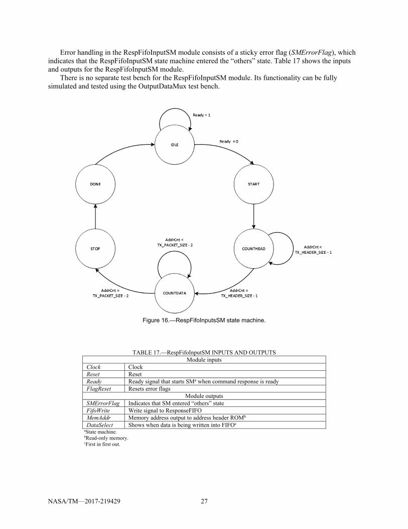
4.1.9 RespFifoInputSM.vhd
This module contains a state machine that controls the writing of command response packets into the ResponseFifo of the TxResponsePackets module. The state machine starts when the Ready input signal goes high. The Ready signal is connected to the TxReady signal in TxResponsePackets.vhd. When the Ready signal goes high, the FIFO write signal (FifoWrite) is raised to allow bytes to be written into the ResponseFifo and sets the DataSelect output signal low to select Ethernet packet headers at the input to the FIFO.
The Memory Address output signal (MemAddr, 6 bits) is used to address the TxPacketROM to write the packet Ethernet headers into the FIFO, and then the DataSelect output signal goes high to multiplex the command response to be written into the FIFO.
The state machine, shown in Figure 16, uses counters to count the number of header bytes and the number of command response bytes that are written.
The RespFifoInputSM module is clocked by a 125 MHz clock.
NASA/TM—2017-219429 27
Error handling in the RespFifoInputSM module consists of a sticky error flag (SMErrorFlag), which indicates that the RespFifoInputSM state machine entered the “others” state. Table 17 shows the inputs and outputs for the RespFifoInputSM module.
There is no separate test bench for the RespFifoInputSM module. Its functionality can be fully simulated and tested using the OutputDataMux test bench.
Figure 16.—RespFifoInputsSM state machine.
TABLE 17.—RespFifoInputSM INPUTS AND OUTPUTS Module inputs
Clock Clock Reset Reset Ready Ready signal that starts SMa when command response is ready FlagReset Resets error flags
Module outputs SMErrorFlag Indicates that SM entered “others” state FifoWrite Write signal to ResponseFIFO MemAddr Memory address output to address header ROMb DataSelect Shows when data is being written into FIFOc
aState machine. bRead-only memory. cFirst in first out.
NASA/TM—2017-219429 28
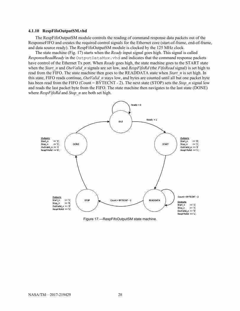
4.1.10 RespFifoOutputSM.vhd
The RespFifoOutputSM module controls the reading of command response data packets out of the ResponseFIFO and creates the required control signals for the Ethernet core (start-of-frame, end-of-frame, and data source ready). The RespFifoOutputSM module is clocked by the 125 MHz clock.
The state machine (Fig. 17) starts when the Ready input signal goes high. This signal is called ResponseReadReady in the OutputDataMux.vhd and indicates that the command response packets have control of the Ethernet Tx port. When Ready goes high, the state machine goes to the START state when the Start_n and OutValid_n signals are set low, and RespFifoRd (the FifoRead signal) is set high to read from the FIFO. The state machine then goes to the READDATA state when Start_n is set high. In this state, FIFO reads continue, OutValid_n stays low, and bytes are counted until all but one packet byte has been read from the FIFO (Count = BYTECNT - 2). The next state (STOP) sets the Stop_n signal low and reads the last packet byte from the FIFO. The state machine then navigates to the last state (DONE) where RespFifoRd and Stop_n are both set high.
Figure 17.—RespFifoOutputSM state machine.

NASA/TM—2017-219429 29
TABLE 18.—RespFifoOutputSM INPUTS AND OUTPUTS Module generic
BYTECNT Total number of bytes in command response Ethernet packet Module inputs
Clock Clock, 125 MHz Reset Reset Ready Starts SMa—low when a response packet is read to be sent FlagReset Resets error flags
Module outputs SMErrorFlag Indicates that SM entered “others” state RspPacketDone High indicates a command response packet is finished FifoRead Read signal to ResponseFIFO StartOfFrame Ethernet packet start-of-frame signal EndOfFrame Ethernet packet end-of-frame signal SourceReady Ethernet packet data source ready signal
aState machine.
Error handling in the RespFifoOutputSM module consists of a sticky error flag (SMErrorFlag),
which indicates that the RespFifoOutputSM state machine entered the “others” state in the state machine navigation case statement. Table 18 shows the inputs and outputs for the RespFifoOutputSM module.
There is no separate test bench for the RespFifoOutputSM module. Its functionality can be fully simulated and tested using the OutputDataMux test bench.
4.1.11 RxStreamingData.vhd
The RxStreamingData module controls the Rx-side streaming data functions of the test waveform. The block diagram for this module is shown in Figure 18. Inputs clocks to this module are a 125 MHz clock for the Ethernet functions and a 196.6 MHz clock for the waveform functions. There is a clock domain crossing that occurs in order to transmit the streaming data (running at 196.6 MHz) over the Ethernet (running at 125 MHz). In Figure 18, the waveform clock domain is shown in blue and the 125 MHz clock domain is shown in orange.
The RxStreamingData module contains two FIFOs that are used for clock domain crossing and the formation of complete packets: StreamingFifo and StreamingDataFifo. Data from the ADC’s I channel is sampled and stored at the waveform word clock rate into the StreamingFifo in 16-bit words. The data is read out of the StreamingFifo at a rate of 1/2 of the 125 MHz Ethernet clock rate (i.e., 62.5 MHz). This output is multiplexed with Ethernet packet headers (from Rx_Streaming_Data_ROM containing TxPacketDataSW8.coe) and written into the StreamingDataFifo in 8-bit bytes. The output of the StreamingDataFifo and associated control signals are sent to the Ethernet EMAC.
Three state machines control the reading and writing of the two FIFOs. The StreamFifoInputSM (see Section 4.1.12) controls the input to the StreamingFifo. The StreamFifoOutputSM (see Section 4.1.13) controls the reading of data from the StreamingFifo, the addressing of the Rx_Streaming_Data_ROM, and the writing of data into the StreamingDataFifo. The StrDataFifoOutputSM (see Section 4.1.15) controls the reading of data from the StreamingDataFifo.
Important inputs to this module are the Enable and OutputStrReady signals (Table 19). The Enable signal is high when a Rx-side streaming data command was correctly received. The Enable signal is synchronized to the waveform clock domain, so that the signal (EnableRegD) can be used to start the StreamFifoInputSM state machine. Another important input signal, OutputStrReady, comes from the OutputDataMux signal called SampleReadReady, which is asserted to give control of the Ethernet Tx port to the RxStreamingData module.
Two important outputs of the RxStreaming data module are StrPacketsDone and StreamReadReady (Table 19). StrPacketsDone indicates to the OutputDataMux that a set of four streaming packets have been sent. The StreamReadReady signal indicates that the StreamingDataFifo has at least 3000 bytes in it and is ready to be read. This signal is used in OutputDataMux (called SampReadReady) to start sending four streaming data packets to the Ethernet Tx port.

NASA/TM—2017-219429 30
Error handling in RxStreamingData consists of three parts: (1) A sticky error flag (SMErrorFlag), which indicates that the RxStreamingData state machine
entered the “others” state in the state machine navigation case statement. (2) The SMErrorFlags from the submodules StreamFIfoInputSM, StreamingFifoOutputSM,
CreatePacketSM, and StrDataFifoOputputSM are passed up to the next level (OutputDataMux) through the RxStreamingData module.
(3) The FIFO full and empty flags (FifoFlags) from the StreamingDataFifo and StreamingFifo are passed up to the next level (OutputDataMux).
Figure 18.—RxStreamingData module. FIFO, first in first out; MUX, multiplexer; ROM, read-only memory.
TABLE 19.—RxStreamingData INPUTS AND OUTPUTS
Module inputs Clock 125 MHz clock Reset Reset (Ethernet clock domain) ResetWF Waveform reset (waveform clock domain) WFClock Waveform clock WFClockEn Waveform clock enable Enable This enable signal starts streaming data OutputStrReady Ready to transmit four streaming packets on Ethernet DataIn 16 bits, data from ADCa FlagReset Resets the error flags
Module outputs SMErrorFlags 4 bits, indicates that the SMb entered “others” state FifoFlags 4 bits, FIFOc full and empty flags StrPacketsDone Indicates a set of four streaming packets are done StreamReadReady Indicates that data is ready to be output DataOut 8 bits, packet data for sample captured data packets to Ethernet DataSof Start-of-frame for sample packets DataEof End-of-frame for sample packets DataReady Source ready for sample Ethernet packets
aAnalog-to-digital converter. bState machine. cFirst in first out.

NASA/TM—2017-219429 31
There is no separate test bench for the RxStreamingData module. Its functionality can be fully simulated and tested using the OutputDataMux test bench.
4.1.12 StreamFifoInputSM.vhd
The StreamFifoInputSM module contains the state machine that controls the writing of streaming data into the StreamingFifo. This module is clocked by the waveform clock.
The StreamFifoInputSM state machine (Fig. 19) starts when Rx-side streaming command is received (i.e., the Enable input signal is high). The StreamingFifo is first reset (states RST1 and RST2) by the state machine before writes are started. This ensures that only good data is stored in the FIFO.
After the reset is issued to the StreamingFifo, the state machine navigates through four 1-clock-cycle wait states to ensure that the reset is done and the StreamingFifo is ready for data. Next, the WRITEDATA state is entered. In this state, the FifoWrite signal is set high to enable FIFO writes. Writes continue until the Enable signal goes low when a stop streaming command is received and processed.
Figure 19.—StreamFifoInputSM state machine.

NASA/TM—2017-219429 32
TABLE 20.—StreamFifoInputSM INPUTS AND OUTPUTS Module inputs
Clock Clock (waveform clock rate) ClockEn Clock enable to allow for rates other than waveform clock rate Reset Reset Enable Signal that enables start of SMa; high when a streaming command is received FlagReset Resets error flags
Module outputs SMErrorFlag SM error flag FifoRst Resets StreamingFifo before data is written into it FifoWrite Active high signal that controls when data is written into StreamingFifo
aState machine.
Error handling in StreamFifoInputSM consists of a sticky error flag (SMErrorFlag), which indicates
that the StreamFifoInputSM state machine entered the “others” state in the state machine navigation case statement. Table 20 shows the inputs and outputs for the StreamFifoInputSM module.
There is no separate test bench for the StreamFifoInputSM module. Its functionality can be fully simulated and tested using the OutputDataMux test bench.
4.1.13 StreamFifoOutputSM.vhd
The StreamFifoOutputSM module state machine controls the reading of data from the StreamingFifo, the formation of four streaming data packets, and the writing of the packet data into the StreamingDataFifo. This module is clocked by the Ethernet clock rate, which is 125 MHz.
The StreamingFifo is written in 16-bit words under the control of the previous module, StreamFifoInputSM (Fig. 19). The Enable input signal to StreamFifoOutputSM (Fig. 20) will be high if a valid Rx-side streaming command was received. Once Enable is high, the state machine waits for the StreamingFifo to partially fill with data. When the StreamingFifo contains 10,000 out of a possible 16,384 bytes, the prog_empty signal goes low. In the RxStreamingData module, this signal is inverted and called ProgAlmostFull, which is high when the StreamingFifo is ready to be read. The ProgAlmostFull signal is called AlmostFull in the StreamFifoOutputSM module. When AlmostFull goes high the first time, the state machine moves to the CREATEPKT1 state.
The CREATEPKT1 state transfers control to the CreatePacketSM state machine (see Section 4.1.14), which controls the formation of streaming packets and the writing of these packets into the StreamingDataFifo. When the CreatePacketSM module is done creating a packet, it raises the PacketDone signal and transfers the StreamFifoOutputSM state machine to the two 1-clock-cycle wait states. Next, the state machine goes to the CREATEPKT2 state to create the second packet, followed by two wait states. This process continues until the fourth packet is created in CREATEPKT4, followed by two wait states (STOP and DONE). The state machine then returns to the IDLE state. If the Enable signal is still high, the state machine will go to the WAITING state to wait for the AlmostFull signal (from the StreamingFifo) to go high again.
The streaming data is written into the StreamingFifo at the waveform word rate, which is much slower than the Ethernet clock rate. Data is read out of the StreamingFifo at one-half the Ethernet clock rate, which is 62.5 MSamples/sec. Because the data is read out faster than it is written into the FIFO, there will be time between each group of four streaming packets while the StreamingFifo fills with streaming data. The StreamingFifo will not underflow because only four packets of data (<2000 bytes) are read out at a time and no additional data is read out until the FIFO fills up to greater than 10,000 words. The StreamingFifo should not overflow, because the data is read out faster than it is written.
One important state machine output signal is called DataEn. The DataEn signal is used for the multiplexer select signal (called DataSel) in the RxStreamingPackets module. Table 21 shows the DataEn values and their associated functions.

NASA/TM—2017-219429 33
Figure 20.—StreamFifoOutputSM state machine.
TABLE 21.—SIGNAL DEFINITION
DataEn Description 0000 Ethernet header 0001 Data from StreamingFifo 0010 Data header for packet number 1 0011 Data header for packet number 2 0100 Data header for packet number 3 0101 Data header for packet number 4
Error handling in StreamFifoOutputSM consists of a sticky error flag (SMErrorFlag), which indicates
that the StreamFifoOutputSM state machine entered the “others” state in the state machine navigation case statement. The SMErrorFlag signal from the submodule CreatePacketSM is passed up to the next level (RxStreamingData) through the StreamFifoOutputSM module. Table 22 shows the inputs and outputs for the StreamFifoOutputSM module.
There are no separate test benches for the StreamFifoOutputSM module. Its functionality can be fully simulated and tested using the OutputDataMux test bench.
4.1.14 CreatePacketSM.vhd
This module works with the state machine in the StreamFifoOutputSM module to create a single packet of Rx streaming data. This module is clocked by the Ethernet clock, which is 125 MHz.
This state machine (Fig. 21) controls the reading of data from the StreamingFifo and multiplexing of data and headers into the StreamingDataFifo. In the COUNTHEAD state, the CreatePacketSM state machine starts an address counter (AddrCnt) to address the Rx_Streaming_Data_ROM, which contains

NASA/TM—2017-219429 34
TABLE 22.—StreamFifoOutputSM INPUTS AND OUTPUTS Module inputs
Clock 125 MHz clock Reset Reset signal Enable Signal to trigger SMa to start AlmostFull Almost full signal from StreamingFifo FlagReset Resets the error flags
Module outputs SMErrorFlags 2 bits, indicates that SM entered “others” state MemAddr 6 bits, address used for the ROMb containing packet header bytes DataSelect 4 bits, MUXc selects signals that indicate to select packet header, sample data, or data headers FifoRead Active high to read from StreamingFifo DataReady Indicates that StreamingDataFifo is full enough to start reads HalfClockEn 50 percent duty cycle of clock signal; used to multiplex 16-bit data from StreamingFifo into 8-
bit data into StreamingDataFifo FifoWrite Active high signal used to write to StreamingDataFifo
aState machine. bRead-only memory. cMultiplexer.
Figure 21.—CreatePacketSM state machine.
the Ethernet header for the streaming packets. A multiplexer controls which type of data is written into the StreamingDataFifo. Refer to the RxStreamingData block diagram in Figure 18 for clarification of how these blocks are interconnected.
First, the Ethernet header bytes (8 bits) are written into the StreamingDataFifo in the COUNTHEAD state. The AddrCnt signal is used to keep track of the number of bytes written into the StreamingDataFifo. Next, the state machine enters the INSDATAHEAD state, where the three payload header bytes are written into the StreamingDataFifo. The three payload header bytes are shown in Figure 22. The third byte, the streaming packet number, is a packet count inserted in the RxStreamingData module. This count is increased by one for each successive packet and can be used in testing to ensure no packets have been dropped.

NASA/TM—2017-219429 35
Figure 22.—Streaming packet payload header structure. ID, identification.
TABLE 23.—CreatePacketSM INPUTS AND OUTPUTS Module inputs
Clock 125 MHz Clock Reset Reset Start Start signal to start SMa DataSourceIn 4 bits, indicates which packet of four is being created FlagReset Resets error flags
Module outputs SMErrorFlag Indicates that SM entered “others” state ReadEn Read enable signal to StreamingFifo HalfClockEn Controls which byte of 16-bit data is written into StreamingDataFifo PktDone Packet done, passes control back to StreamingFifoOutputSM MemAddr 6 bits, address to get Ethernet header out of ROMb OutValid_n Low when data into StreamingDataFifo is valid DataSourceOut 4 bits, DataSelect vector to choose which type of data is written into
StreamingDataFifo (data, Ethernet header, or payload header) aState machine. bRead-only memory.
After the payload header is written into the StreamingDataFifo, reads from the StreamingFifo are
started. The output of the StreamingFifo is 16 bit and is read at a frequency of 62.5 MHz. The input to the StreamingDataFifo is 8 bits and is written at a frequency of 125 MHz. The rate difference allows for one 16-bit word to be read from the StreamingFifo in the time it takes to write two 8-bit bytes into the StreamingDataFifo. When writing streaming data into the StreamingDataFifo, the CreatePacketSM state machine alternates between two states, COUNTDATA and COUNTDATAb. In COUNTDATA, a signal called HalfClockEnable is set high. In COUNTDATAb, HalfClockEnable is set low. HalfClockEnable controls a multiplexer to select which byte of the 16-bit data out of the StreamingFifo is written into the StreamingDataFifo. The least significant byte (LSB) is written first and the most significant byte (MSB) is written second. When the AddrCnt value reaches the size of a streaming packet (TX_DATA_PACKET_SIZE-1), the state machine enters the last state, DONE, where the PktDone signal is set high and control is returned to the StreamFifoOutputSM state machine.
Error handling in CreatePacketSM consists of a sticky error flag (SMErrorFlag), which indicates that the CreatePacketSM state machine entered the “others” state in the state machine navigation case statement. Table 23 shows the inputs and outputs for the CreatePacketSM module.
There are no separate test benches for the CreatePacketSM module. Its functionality can be fully simulated and tested using the OutputDataMux test bench.
4.1.15 StrDataFifoOutputSM.vhd
The StrDataFifoOutputSM module controls the reads from the StreamingDataFifo, which contains packetized streaming data. The streaming data is read in groups of four packets at a time.
The state machine reads out a packet, creates signals required by the Ethernet core (end-of-frame, start-of-frame, and data source ready), and adds a short time delay between each packet. This module is clocked by the Ethernet clock, which is 125 MHz.

NASA/TM—2017-219429 36
Figure 23.—StrDataFifoOutputSM state machine.
The state machine (Fig. 23) reads a packet out of the StreamingDataFifo, waits for a short delay, and then repeats until four packets have been read. Then, it tests to see if streaming data has been disabled. If so, it stops and goes to IDLE. Otherwise, it reads out four more packets.
This paragraph describes how the state machine works. First, when an Rx-side streaming command is received, the StrEn input is set high. The state machine will exit the IDLE state and go to two states, RSTFIFO and RSTFIFO2, to reset the StreamingDataFifo to clear it before new data is written into it. Next, the state machine enters the WAIT4EN state to wait for the Enable input to go high and navigates to the WAIT4DATA state. When the StreamingDataFifo is full enough to be read, the Ready signal goes high and navigates to the START state. In the START state, StreamingDataFifo reads begin and the Start_n (start-of-frame) signal is set low. Next, the state machine goes to the READDATA state where the rest of the packet (except for the last byte) is read out of the FIFO and the Start_n signal is set high. Then, in the STOP state, the last packet byte is read and the Stop_n signal is set low. Next, the state machine enters the WAITING state, which waits for 25 clock cycles to put space between each packet. In the next state, DONE, the packet count is checked. If fewer than four packets have been read, the state machine returns to the START state to read out another packet. Otherwise, it will navigate to the FINISH state. If streaming data is still enabled (StrEn = 1), then the state machine will move to the WAIT4EN state to wait for Enable = 1.

NASA/TM—2017-219429 37
Error handling in StrDataFifoOutputSM consists of a sticky error flag (SMErrorFlag), which indicates that the StrDataFifoOutputSM state machine entered the “others” state in the state machine navigation case statement. Table 24 shows the inputs and outputs for the StrDataFifoOutputSM module.
There are no separate test benches for the StrDataFifoOutputSM module. Its functionality can be fully simulated and tested using the OutputDataMux test bench.
4.1.16 ClockEnables.vhd
The ClockEnables module uses generics to create three different clock enable signals. This module can be used by the waveform developer to generate the clock enable signals required for the waveform implementation. The wrapper contains two instances of the ClockEnables module: TxClockEnables for the Tx-side waveform and RxClockEnables for the Rx-side waveform. TxClockEnables is clocked by the DAC sample clock, and RxClockEnables is clocked by the ADC sample clock, both of which are approximately 196.6 MHz. Table 25 shows the inputs and outputs for the ClockEnables module.
The test bench for this module is ClockEnables_tb.vhd. This test bench set the EndCount values for the three clock enable generators in the ClockEnable module and allows the user to see the generated ClockEn signals. The wave configuration file is ClockEnables.wcfg.
TABLE 24.—StrDataFifoOutputSM INPUTS AND OUTPUTS
Module generics ByteCnt Size of streaming packets in bytes CountSize Counts number of bytes in a packet WaitCntSize Counts wait time between packets in a group PacketCntSize Counts number of data packets sent in a group
Module inputs Clock 125 MHz Clock Reset Reset StrEn Streaming enable signal from a streaming command Enable Ready to transmit four streaming packets from OutputDataMux Ready Active high signal that starts SMa; comes from the fill level of StreamingDataFifo;
is high when StreamingDataFifo ReadDataCnt >= 0xBB8 FlagReset Resets error flags
Module outputs SMErrorFlag Flag that indicates SM entered “others” state FifoRead FIFOb read signal StartOfFrame Start-of-frame; used for EMACc; low for first byte of packet EndOfFrame End-of-frame; used for EMAC; low for last byte of packet SourceReady Data source ready; used for EMAC; low during the packet data RstDataFifo Resets the StreamingDataFifo after data is read out StrPacketsDone Indicates a set of four streaming packets are done
aState machine. aFirst in first out. bEthernet Media Access Controller.
TABLE 25.—ClockEnables INPUTS AND OUTPUTS
Module generics EndCount1 Count value for ClockEn1 EndCount2 Count value for ClockEn2 EndCount3 Count value for ClockEn3
Module inputs Clock System clock Reset Active high reset
Module outputs ClockEn1 Output enable ClockEn2 Output enable2 ClockEn3 Output enable3

NASA/TM—2017-219429 38
4.2 STRS_Waveform.vhd
The STRS_Waveform module is the top module for the implementation of the test waveform. An STRS test waveform is required to exercise every interface in the FPGA wrapper to demonstrate its functionality. A waveform developer would remove this module and replace it with his or her custom waveform module.
This test waveform in the STRS_Waveform module performs the following functions:
Decodes received commands and implements the appropriate functionality. Generates sine and cosine waves for the I and Q inputs to the DAC. Strips headers off of streaming Tx-side data packets. Routes Tx-side streaming data to the BERT for checking to test working
Tx-side streaming. Routes Tx-side streaming data to the DAC or loopback to the Rx side for creating
Rx-side streaming data packets. Creates Rx-side streaming data packets from either PRBS data or received ADC data. The STRS_Waveform module has three input clocks: (1) Clk125 (125 MHz Ethernet clock) (2) Tx-side waveform clock (approx. 196.6 MHz) (3) Rx-side waveform clock (approx. 196.6 MHz) Four clock enable signals are used to control the clocking of the waveform functions: two for the Tx
side and two for the Rx side. Two of the clock enable signals, TxWFClockEn2 and RxWFClockEn2, are used for the vast majority of the waveform functions. The TxWFClockEn2 and RxWFClockEn2 signals are used for the 8-bit PRBS generator (PrbsTx23.vhd) and the 8-bit BERT (PrbsRx23.vhd) modules. Clock domain crossings occur in the following submodules—TxStreamData, CommandDecoder, and ClockDomainCrossing. See each submodule description for clock domain crossing details.
The Tx-side waveform block diagram, shown in Figure 24, contains CommandParse, TxStreamData, CommandDecoder, SineWaveGen, and TransmitSignal modules. The CommandParse module parses received commands and outputs the Command ID and Command Data from the received command. The CommandDecoder inputs the command ID and command data from CommandParse and creates the appropriate command action. TxStreamData receives streaming data packets from the processor and extracts the data from the packets. The SineWaveGen module generates sine waves for the I and Q DAC inputs on the RF front end-board. TransmitSignal creates PRBS data.
The Rx-side waveform block diagram, shown in Figure 25, contains the ReceiveSignal module and registers. The ReceiveSignal module contains a BERT and a multiplexer that selects between incoming data either from the ADC or a loopback data signal from the Tx side of the waveform.
Error flags and FIFO full and empty flags within the STRS_Waveform module and its submodules are combined with the incoming the StatusBits from the wrapper into one 40-bit StatusBitsR signal, which is sent to the CommandDecoder module to be transmitted in a response to a Status command. Table 26 shows the bit definition for all the status bits.

NASA/TM—2017-219429 39
Figure 24.—Tx-side waveform. Clk, clock.
Figure 25.—Rx-side waveform. PRBS, pseudorandom bit sequence; Tx, transmit.

NASA/TM—2017-219429 40
TABLE 26.—DEFINITION OF StatusBits (ERROR FLAGS) Bit Definition Description 0 Sync Lost BERTa lost synchronization 1 SyncLossCnt(0) Number of times a sync loss occurred 2 SyncLossCnt(1) 3 SyncLossCnt(2) 4 SyncLossCnt(3) 5 SyncLossCnt(4) 6 SyncLossCnt(5) 7 SyncLossCnt(6) 8 SyncLossCnt(7) 9 open 10 open 11 EthernetRx SM StuckFlag Indicates EthernetRx SMb is stuck 12 ResponsePktFifo_Full ResponsePktFifo overflow and underflow
indicators 13 StreamingFifo_Full StreamingFifo overflow and underflow
indicators 14 StreamingFifo_Empty 15 Streaming_Data_Fifo_Full StreamingDataFifo overflow and underflow
indicators 16 Streaming_Data_Fifo_Empty 17 StreamingDataFifo_Full StreamingDataFifo overflow and underflow
indicators 18 StreamingDataFifo_Empty 19 SMFailure_ResetGen Flags indicating that particular SM (indicated in
name of flag) erroneously entered “others” state 20 SMFailure_EthernetRx 21 SMFailure_RxCommandPackets 22 SMFailure_RxStreamingPackets 23 SMFailure_RespFifoOutputSM 24 SMFailure_StreamFifoInputSM 25 SMFailure_CreatePacketSM 26 SMFailure_StreamFifoOutputSM 27 SMFailure_StrDataFifoOutputSM 28 SMFailure_OutputDataMux 29 SMFailure_TxStreamData 30 SMFailure_CommandParse 31 SMFailure_PrbsRx23_Wrapper 32 SMFailure_BertSyncherSM 33 SMFailure_ReceiveSignal 34 SMFailure_TxStreamFifoWriteSM 35 SMFailure_RespFifoInputSM 36 SMFailure_PulseGenSM 37 SMFailure_StatusResetGenSM 38 TxSidePacketError(CmdParse) Indicates that received packet was shorter than
expected 39 EmacRxError Rxc error on EMACd IPe
aBit error rate tester. bState machine. eReceive. dEthernet Media Access Controller. eInternet Protocol.

NASA/TM—2017-219429 41
TABLE 27.—STRS_Waveform INPUTS AND OUTPUTS Module inputs
Clk125 125 MHz clock TxWFClock Tx-side waveform clock (approx. 196.6 MHz, DACa clock) TxWFClockEn1 Tx-side waveform clock enable (byte rate) TxWFClockEn2 Tx-side waveform clock enable (word rate) RxWFClock Rx-side waveform clock (approx. 196.6 MHz, ADCb clock) RxWFClockEn1 Rx-side waveform clock enable (byte rate) RxWFClockEn2 Rx-side waveform clock enable (word rate) SymbClockEn Symbol rate clock enable Reset Reset signal from the wrapper (power-on-reset and push button) DIP_SW 8 bits, dip switches onboard RxCmdDataIn 8 bits, received command data RxCmdDataSrcRdy Received command data valid signal StreamDataIn 8 bits, received streaming data StreamDataValid Received streaming data valid signal EmacRxError EMACc PHYd receive error StatusBitsIn 36 bits, status bits coming from wrapper RespSending_n Low while a command response is being sent AdcDataInI ADC Ie channel data AdcDataInQ ADC Qf channel data
Module outputs DacDataOutI DAC I channel data DacDataOutQ DAC Q channel data WFResetOut Waveform reset signal FlagResetOut Status bits reset signal CmdResponse 120-bit contents of response to a command TxSendReady Indicates that a command response can be sent StreamEnRx Stream enable, stays high until streaming is stopped RxParallelData 16 bits, data to be streamed LED 8 bits, outputs to board LEDsg
aDigital-to-analog converter. bAnalog-to-digital converter. cEthernet Media Access Controller. dPhysical layer. eIn-phase. fQuadrature. gLight-emitting diodes.
The STRS_Waveform module also contains two processes (CntBytes and RespSendStart), which
work together to create an active-low signal called TxSendReady that indicates a command response packet is ready to be sent.
Table 27 shows the inputs and outputs for the STRS_Waveform module. There is no separate test bench for the STRS_Waveform module.
4.2.1 ClockDomainCrossing.vhd
The ClockDomainCrossing module registers multiple signals with the appropriate clock to allow these signals to cross the clock domain. Most of the signals that need to cross the clock domain are created in the 125 MHz clock domain as the result of a received command. These signals must cross the clock domain to the waveform clock domain to control the appropriate functions. Therefore, most of the signals that cross the clock domain are passed into the ClockDomainCrossing module through the CmdRegister input signal vector that was created in the CommandDecoder module. The definition of the bits within the CmdRegister vector can be found in Section 4.2.5.

NASA/TM—2017-219429 42
TABLE 28.—ClockDomainCrossing INPUTS AND OUTPUTS Module inputs
Clk125 125 MHz clock TxWFClock Txa-side waveform clock TxWFClockEn Tx-side waveform clock enable RxWFClock Rxb-side waveform clock Reset Reset SoftReset Soft reset from reset command CmdRegister 16 bits, command register
Module outputs SoftResetOut Registered soft reset (125 MHz clock domain) WFResetOut Waveform reset (waveform clock domain) MainReset Main reset (125 MHz clock domain) SourceSelectR 2 bits, source select (waveform clock domain) PrbsEnableR PRBSc generator (waveform clock domain) BertEnableR Enable BERTd (waveform clock domain) ErrorInsertR Insert a single error (waveform clock domain) LoopbackCtrlR Loopback (waveform clock domain) StreamEnRx Enable Rx-side streaming (waveform clock domain) StartWFR Registered start waveform signal (waveform clock
domain) aTransmit. bReceive. cPseudorandom bit sequence. dBit error rate tester. eWaveform.
Other key signals are created from the Reset and SoftReset input signals. The Reset and SoftReset
signals are combined (OR’d) into a ComboReset signal. The ComboReset signal is then double registered in the 125 MHz clock domain to create the MainReset signal and double registered in the waveform clock domain to create the WFReset signal. Table 28 shows the inputs and outputs for the ClockDomainCrossing module.
There is no separate test bench for the ClockDomainCrossing module.
4.2.2 TxStreamData.vhd
The TxStreamData module is part of the STRS waveform and is used to receive streaming data packets from the processor. The purpose of this module is to cross the clock domain between the Ethernet packet byte rate (125 MHz) on the input to the waveform word clock rate on the output of the module. A FIFO (called StreamingDataFifo) is used to accomplish this purpose. Additionally, the FIFO will allow the “bursty” input data to be output in continuous words. The outputs of this module are 16-bit data words and a data valid signal that is high when the output data is valid.
A state machine, TxStreamFifoWriteSM, is used to control the writing of data into the FIFO. Received streaming Ethernet data is in 8-bit bytes and needs to be written into the FIFO in 16-bit words. The state machine combines two Ethernet bytes into one 16-bit word and writes it into the FIFO. See Section 4.2.3 for more information about the TxStreamFifoWriteSM module.
A block diagram of the TxStreamData module is shown in Figure 26. Using the StreamDataValid signal as the FIFO write enable signal, incoming data is written into the FIFO only during the payload portion of the streaming data. The StreamDataIn (8 bits) is written into FIFO using the 125 MHz clock rate.
A state machine (Fig. 27) controls the reading of data from the FIFO. The FIFO reads start when the prog_empty signal (a read-side signal currently set to 98,750, 16-bit words) indicates that the FIFO is full enough to start FIFO reads. The prog_empty signal is inverted to create a new signal called Threshold. FIFO reads continue unless the Enable input signal goes low from a received command that stops Tx-side streaming. To prevent FIFO underflows, reads will stop when the FIFO AlmostEmpty signal goes high and will restart again when if the Threshold signal goes high again.

NASA/TM—2017-219429 43
Figure 26.—TxStreamData. FIFO, first in first out.
Figure 27.—TxStreamData state machine.
To prevent potential FIFO overflows or underflows, and thus the interruption of continuous streaming data at the output of the TxStreamData module, three status signals are created.
(1) Fifo3QtrFull signal indicates that the FIFO is 3/4 full. (2) Fifo1QtrFull signal indicates that the FIFO is 1/4 full. (3) FifoCenter signal indicates when the FIFO level is in the middle (i.e., between 1/4 full and 3/4 full).
These three signals are outputs of the TxStreamData module and are routed in the STRS_Waveform module to the CommandDecoder module. The three status signals will be transmitted to the processor in a response to a TxStreamingFifoLevel command. The general purpose processor (GPP) uses the FIFO status signals with its packet transmission algorithm to control the rate at which it sends streaming data packets to the FPGA to avoid loss of data.

NASA/TM—2017-219429 44
TABLE 29.—TxStreamData INPUTS AND OUTPUTS Module inputs
EthClock Ethernet clock (125 MHz) WFClock Waveform clock Reset Reset Enable Txa-side streaming enable StreamDataIn 8 bits, streaming data with headers removed StreamDataValid High indicates StreamDataIn is valid FlagReset Resets the error flags
Module outputs SMErrorFlag Indicates that SMb entered “others” state FifoFlags 2 bits, FIFOc full (bit 0) and empty (bit 1) flags Fifo3QtrFull FIFO 3/4 full in Ethernet clock domain Fifo1QtrFull FIFO 1/4 full in Ethernet clock domain FifoCenter FIFO level is between 1/4 full and 3/4 full DataOut 16 bits, output data words DataOutValid High when DataOut is valid
aTransmit. bState machine. cFirst in first out.
Error handling in TxStreamData consists of two parts: (1) An error flag (SMErrorFlag), which indicates that the TxStreamData state machine entered the
“others” state in the state machine navigation case statement. (2) A pass-through of the FIFO full and empty flags (FifoFlags). Table 29 shows the inputs and outputs for the TxStreamData module. The test bench for this module is named TxStreamData_tb.vhd. It creates input signals by
reading streaming data and a StreamDataValid control signal from a file called StreamingDataNoHeader.txt. The wave configuration file is TxStreamData.wcfg.
4.2.3 TxStreamFifoWriteSM.vhd
The TxStreamFifoWriteSM module controls writing of Ethernet data (8 bits) into the StreamingDataFifo 16 bits at a time. Input Ethernet data is registered to create a 1-clock-cycle delay so that two bytes can be combined into one word. The state machine controls the registering of the two bytes together and creates a corresponding WriteEnable signal so that the 16-bit word can be written into the FIFO. The state machine diagram is shown in Figure 28.
Error handling in TxStreamFifoWriteSM consists of an error flag (SMErrorFlag), which indicates that the TxStreamFifoWriteSM state machine entered the “others” state in the state machine navigation case statement. Table 30 shows the inputs and outputs for the TxStreamFifoWriteSM module.
The test bench for this module is TxStreamFifoWriteSM_tb.vhd. It creates sample streaming input data in a “brute force” method, so the process writing words into the FIFO can be observed. The wave configuration file is TxStreamFifoWriteSM.wcfg.

NASA/TM—2017-219429 45
Figure 28.—TxStreamFifoWriteSM state machine.
TABLE 30.—TxStreamFifoWriteSM INPUTS AND OUTPUTS Module inputs
EthClock Ethernet clock (125 MHz) Reset Reset FlagReset Resets error flags StreamEnable Txa-side streaming enable DataValid Indicates with DataIn is valid DataIn Input data, 16 bits
Module outputs SMErrorFlag Indicates that SMb entered “others” state FifoReset FIFOc reset WriteEn FIFO write enable DataOut 16 bits, output data words
aTransmit. bState machine. cFirst in first out.

NASA/TM—2017-219429 46
4.2.4 CommandParse.vhd
This module parses the Command Packets (payload portion) to extract the command header, the command ID, and the command data. Inputs are the received data from RxPackets.vhd in 8-bit bytes with an active-high DataValid signal. The Ethernet headers are removed from the packet before it reaches the CommandParse module. The CommandParse is clocked by a 125 MHz clock.
A state machine (Fig. 29) implements the CommandParse module functions: extracting the Command ID and Command Data from the packet. The state machine starts when the DataValid signal goes high. The state machine navigates to the GETHEADER state, where the header (0xAA) is removed. Next, the state machine goes to the GETCMDID state, where the Command ID is extracted from the packet. Then, the state machine goes to the GETDATA state, where the data portion of the command is extracted.
If the DataValid signal goes low before the expected end of the command packet, the state machine navigates to the ERROR state to prevent bad commands from being parsed. During the ERROR state, an error flag (CmdError) is set high.
Key outputs of this module are the CommandID (8 bits), the CmdData (40 bits), and an active-high signal called OutReady that indicates when the CmdData and CommandID are valid.
Figure 29.—CommandParse state machine.

NASA/TM—2017-219429 47
TABLE 31.—CommandParse INPUTS AND OUTPUTS Module inputs
Clock 125 MHz clock Reset Reset DataValid Indicates an Ethernet command is being received RxData 8 bits, received data 8-bit parallel FlagReset Resets error flags
Module outputs SMErrorFlags 2 bits, indicates that SMa entered “others” state OutReady High indicates command data and command IDb are valid CmdIdOut 8 bits, command ID from received packet CmdData 40 bits, command data (payload) from received packet
aState machine. bIdentification.
Error handling for the CommandParse module consists of two parts: (1) An error flag (SMErrorFlag), which indicates that the CommandParse state machine entered the
“others” state in the state machine navigation case statement. (2) An error flag called CmdError that is high if the state machine enters the ERROR state. The flags are output from the module in the signal SMErrorFlags, a 2-bit signal. SMErrorFlag is
bit 0 and CmdError is bit 1. Table 31 shows the inputs and outputs for the CommandParse module. The test bench for this module is CommandParse_tb.vhd. It creates sample command data in a
“brute force” method. The wave configuration file is CommandParse.wcfg.
4.2.5 CommandDecoder.vhd
A block diagram of the CommandDecoder module is shown in Figure 30. This module receives the CommandID and the CommandData from the CommandParse module, and it decodes the command to determine and implement the desired action. The command structure is shown in Table 32, and a list of all the possible commands and their formats are shown in Table 33.
The CommandDecoder is clocked by a 125 MHz clock. There are two inputs signals to this module (BertBits and BertErrors) that cross the clock domain from the waveform clock domain to the 125 MHz domain. This is handled by double registering the BertBits and BertErrors signals with the 125 MHz clock when they enter the CommandDecoder module. There is another clock domain crossing in the CommandDecoder. The KnightRider submodule runs on the waveform clock rate. The output of the KnightRider module (KRLeds) is double registered with the 125 MHz clock crosses the clock domain to allow KRLeds to be combined with other signals before setting the onboard LEDs.
The primary process in the module is the ExecuteCmd process, which is a large case block that uses the CommandID signal to select the correct “when” block to execute. Each “when” block in the case block forms a 120-bit command response packet (ResponseO, see Table 14 for the format) and sets appropriate control signals based upon the CommandID and CommandData received.
In addition to the ResponseO signal, the following key signals are set in the case statement “when” blocks:
(1) SendReset, which set high when a Soft Reset command is received. (2) LedsOut, which sets the FPGA board LED bank. (3) StatusReset, which is set high when a Status command is received. (4) CommandReg, a 16-bit vector which is used to control functions within the waveform. The bits within the CommandReg signal are set according to the received command. Table 34 shows
the definition of the bits in the CommandReg signal.

NASA/TM—2017-219429 48
Figure 30.—CommandDecoder module. LEDs, light-emitting diodes; MUX, multiplexer.
TABLE 32.—COMMAND STRUCTURE Byte number Description
1 Header byte (0xAA) 2 Command IDa 3 Data (MSBb) 4 Data 5 Data 6 Data 7 Data (LSBc)
aIdentification. bMost significant byte. cLeast significant byte.

NASA/TM—2017-219429 49
TABLE 33.—COMMANDS Description Header
byte 1 Command IDa byte 2
Byte 3 Bytes 4 to 7
Null command—do nothing 0xAA 0x00 0x00 0x00
Reset 0xAA 0x01 0x00 0x00
Start waveform 0xAA 0x06 0x00 0x00
Stop waveform 0xAA 0x07 0x00 0x00
Start PRBSb generator 0xAA 0x08 0x00 0x00
Enable BERTc 0xAA 0x09 0x00 0x00
Test command 0xAA 0x0C 0xXX (LEDd value) 0x00
Stream forward data 0xAA 0x0D 0x00 0x00
Stream return data 0xAA 0x0E 0x00 0x00
Insert error in PRBS 0xAA 0x0F 0x00 0x00
Stop PRBS generator 0xAA 0x10 0x00 0x00
Disable BERT 0xAA 0x11 0x00 0x00
Select Txe data source 0xAA 0x13
0x00 = sine wave 0x01 = PRBS
0x02 = streaming sine 0x03 = streaming PRBS
0x00
Select Rxf data source 0xAA 0x14 0x00 = ADCg
0x01 = loopback 0x00
Stop Rx-side streaming data 0xAA 0x15 0x00 0x00
Stop Tx-side streaming data 0xAA 0x16 0x00 0x00
Start Rx-side PRBS generator 0xAA 0x17 0x00 0x00
Stop Rx-side PRBS generator 0xAA 0x18 0x00 0x00
Tx StreamingFifo level 0xAA 0xF9 0x00 0x00
Request status bits 0xAA 0xFA 0x00 0x00
Request telemetry (BERh data)
0xAA 0xFB 0x00 0x00
Request telemetry (dip switch value)
0xAA 0xFC 0x00 0x00
Request telemetry (waveform running or stopped)
0xAA 0XFD 0x00 0x00
aIdentification. bPseudorandom bit sequence. cBit error rate tester. dLight-emitting diode. eTransmit. fReceive. gAnalog-to-digital converter. hBit error rate.

NASA/TM—2017-219429 50
TABLE 34.—COMMAND REGISTER BIT DEFINITION Bit number Description Definition
1 Enable Rx-side PRBSa 1 = running, 0 = stopped 3 Waveform running 1 = running, 0 = stopped 5 Insert PRBS error 1 = insert error, 0 = no error 6 Enable Txb-side PRBS 1 = enabled, 0 = disabled 7 Enable BERTc 1 = enabled, 0 = disabled 8 and 9 Tx source select 00 = sine, 01 = PRBS, 10 = streaming sine,
11 = streaming PRBS 12 Stream enable Tx 1 = enabled, 0 = disabled 13 Stream enable Rxd 1 = enabled, 0 = disabled 14 and 15 Rx source select 00 = ADCe, 01 = loopback
aPseudorandom bit sequence. bTransmit. cBit error rate tester. dReceive. eAnalog-to-digital converter.
TABLE 35.—LedOut BIT DEFINITION
Bit number Definition 0 to 3 KnightRider flashing lights when waveform is running
4 EMACa receive error (from PHYb error signal) 5 to 7 Unused
aEthernet Media Access Controller. bPhysical layer.
A reset command creates a soft reset pulse to the waveform logic. Although a response command is
created by decoding this command, it will never be sent since the reset pulse clears signals that would cause a response command to be sent. This is understood and treated accordingly by the STRS code. When a reset command is received, the CommandDecoder module sets SendReset high. This signal is converted to a pulse (ResetOut) using the PulseGenSM module. This ResetOut signal resets the waveform logic, but not the wrapper.
The bank of LEDs on the FPGA board are used to provide a visual indication of some of the functions of the waveform and are set with the LedsOut signal. Table 35 shows the definition of the bits in the LedsOut signal. The KnightRider module creates flashing lights on the four least significant bits of the LED bank to show when the waveform is running.
The StatusReset signal is created when a Request Status Bits command is received. This signal is used to create the FlagResetOut signal that clears all the “sticky” status bits in the wrapper and the waveform. The FlagResetOut signal is created in the submodule StatusResetGenSM, a state machine that is started when StatusReset goes high.
The case statement that decodes all the commands contains command validation to make sure the received commands are valid and issued in the appropriate order. For example, a BER command will be rejected if the BERT is not running, and a TxConfigure command will be rejected if the waveform is currently running (so you cannot change the data rate while the waveform is running). The format of a rejected command is shown in Table 15. A rejected command response packet will also be sent if an unknown Command ID is received.
Input signals, BertBits and BertErrors, come from the ReceiveSignal module, which runs off of the Rx-side waveform clock. These signals cross clock domains in CommandDecoder and therefore are synchronized to the 125 MHz clock with a double register to transmit this information in a response packet as a result of a received BER Data command.
Error handling in the CommandDecoder module consists of registering and combining the error flags generated from the wrapper submodules, the waveform submodules, and from the CommandDecoder submodules (PuleGenSM and StatusResetGenSM) into a single 40-bit word called StatusBits. The StatusBits signal is sent to the processor in response to a Request Status Bits command. Table 36 shows the inputs and outputs for the CommandDecoder module.

NASA/TM—2017-219429 51
TABLE 36.—CommandDecoder INPUTS AND OUTPUTS Module inputs
Clock 125 MHz clock Reset Reset from FPGAa board CmdIdIn 8 bits, command IDb from CommandParse module CmdDataIn 40 bits, command data from CommandParse module InputValid High indicates command data and command ID from CommandParse are valid DipSwitches 8 bits, dip switch bank from the FPGA board WFClock Waveform clock WFClockEn Waveform clock enable BertBits 64 bits, total bits received from BERTc BertErrors 32 bits, total bits in error from BERT Fifo3QtrFull FIFOd 3/4 full in Ethernet clock domain Fifo1QtrFull FIFO 1/4 full in Ethernet clock domain FifoCenter FIFO level is near center EmacRxError EMACe PHYf receive error StatusBitsIn 40 bits, status bits coming from the waveform RespSending_n Low while a command response is being sent
Module outputs Leds 8 bits, LEDg bank on the FPGA board FlagResetOut Reset for status bits Response 120 bits, contents of the response to a command CmdRegOut 16 bits, command register, a register that enables or disables waveform functions ResetOut Reset caused by reset command Done Indicates end of a packet and that output data is ready
aField-programmable gate array. bIdentification. cBit error rate tester. dFirst in first out. eEthernet Media Access Controller. fPhysical layer. gLight-emitting diode.
The test bench for this module is named CommandDecoder_tb.vhd. The test bench sets the value
of CmdDataIn and then changes the CmdIdIn value so that the response can be observed. The wave configuration file is CommandDecoder.wcfg.
4.2.6 StatusResetSM.vhd
The StatusResetSM module (a submodule to CommandDecoder) creates the FlagResetOut signal in the CommandDecoder module that clears all the status bit flags in the waveform and the wrapper. The StatusResetSM is clocked by the 125 MHz clock.
The StatusResetSM state machine creates a signal (Output) that is 5 clock cycles wide (high) when the input signal Enable (StatusReset in CommandDecoder) goes high.
The state machine (diagram in Fig. 31) starts in the IDLE state with a power-on-reset or push button reset, causing a Reset signal to go high. When the Reset signal goes low (is de-asserted), the state machine goes through four wait states, each one cycle long. During states WAIT3 and WAIT4, a FlagReset signal is asserted. This FlagReset is only for startup purposes and is done to clear any error flags that become erroneously set during a reset. The state machine then navigates to a fifth wait state (WAIT5). In the CommandDecoder module, the Enable signal is connected to a StatusReset signal that is high when a Request Status command is received. The state machine will stay in WAIT5 until the Enable input signal goes high and then go to the WAIT4RESP state.

NASA/TM—2017-219429 52
Figure 31.—StatusResetSM state machine.
TABLE 37.—StatusResetSM INPUTS AND OUTPUTS Module inputs
Clock Clock signal Reset Reset (asserted low) Enable Starts SMa when it goes high RespSending_n Low while a command response is being sent
Module outputs SMErrorFlag Indicates that SM entered “others” state Output Output signal—a pulse that is high for five clock cycles
aState machine.
The input signal RespSending_n is low while a command response is being sent over the Ethernet port. When the RespSending_n signal goes low, the state machine navigates to the WAIT4SENT state. The state machine then waits for the RespSending_n signal to go high to navigate to the SET state, where the FlagReset signal is asserted. It will stay in this state until the counter reaches a count of four and then enters the RST state, where the FlagReset signal is de-asserted. When Enable = 0, the state machine will return to the WAIT4RESP state.
Error handling in StatusResetSM consists of a sticky error flag (SMErrorFlag), which indicates that the StatusResetSM state machine entered the “others” state in the state machine navigation case statement. Table 37 shows the inputs and outputs for the StatusResetSM module.
There is no separate test bench for the StatusResetSM module.

NASA/TM—2017-219429 53
4.2.7 PulseGenSM.vhd
The PulseGenSM module (a submodule to CommandDecoder) creates a signal (Output) that is high for five clock cycles when the input signal Enable goes high. This module is used by the CommandDecoder module to create a soft reset pulse when a reset command is received. The PulseGenSM is clocked by the 125 MHz clock.
The state machine (shown in Fig. 32) is very simple. When Enable goes high, the state machine goes to the SET state where Output is set high until Count = 4, when it goes to the RESET state. It will set the Output signal low in RESET and wait for Enable to go low to return to IDLE. Waiting for Enable to go low prevents multiple soft reset pulses from being issued.
Error handling in the PulseGen module consists of a sticky error flag (SMErrorFlag), which indicates that the PulseGen state machine entered the “others” state in the state machine navigation case statement. Table 38 shows the inputs and outputs for the PulseGen module.
There is no separate test bench for the PulseGen module.
Figure 32.—PulseGen state machine.
TABLE 38.—PulseGen INPUTS AND OUTPUTS Module inputs
Clock Clock signal Reset Reset (asserted low) Enable Starts SMa when it goes high FlagReset Resets error flags
Module outputs SMErrorFlag Indicates that SM entered “others” state Output Output signal—a pulse that is high for five clock cycles
aState machine.

NASA/TM—2017-219429 54
4.2.8 KnightRider.vhd
The KnightRider module (a submodule to CommandDecoder) is used to create a “KnightRider” effect on four LEDs to indicate that the waveform is running. This module was created by Tom Bizon for a previous project and was used for the iPAS STRS radio.
The KnightRider module is clocked by the Tx-side waveform clock. The KnightRider input Stop is connected to the inverted waveform running signal (not
CmdRegister(3)) in the CommandDecoder, so that the LEDs will turn off when the waveform is stopped. The SendTNSPkt input is connected to the Tx-side waveform rate (not CmdRegister(0)) in CommandDecoder. SendTNSPkt sets a divide ratio that affects the speed that the LEDs flash at. The Count_n input signal (a count enable) is connected and asserted (set to zero) when a down counter in CommandDecoder reaches all zeroes. The counter starts at 0xFFFF and counts down at the Tx-side waveform rate. This counter is used to slow down the LED KnightRider effect so that rate changes can be seen. Table 39 shows the inputs and outputs of the KnightRider module.
There is no separate test bench for the KnightRider module.
4.2.9 SineWaveGen.vhd
This module generates a 16-bit sine wave signal. The generated sine wave has 128 samples per cycle, clocked at a rate of 1.54 MHz, so it creates a sine wave with a frequency of 24 KHz. The SineWaveGen is clocked by the Tx-side waveform clock. This sine wave is used only when running the iPAS radio in loopback (bypassing the RF front end). The TransmitSignal module contains a separate two tone generator that creates a sine wave that can be used as an input to the I and Q DACs.
The sine is created using a look up table (LUT) called SINE_LUT1, which is defined in STRS_Radio_Pkg.vhd. The LUT contains the first 1/4 cycle of the sine wave. The CreateSine process uses the 1/4 wave to create a full sine wave signal called TwoToneOutput, which is reassigned to the output signal called SineData. The module is clocked by the Tx-side waveform clock. ClockEn is used as clock enable signal that will enable rates slower than input Clock signal.
The Enable input signal to this module is the waveform enable signal created when a Start Waveform command is received. The output of this module is the 16-bit SinData signal. Table 40 shows the inputs and outputs for the SineWaveGen module.
TABLE 39.—KnightRider INPUTS AND OUTPUTS
Module inputs Clk Clock Rst Reset Enable Enable (used to enable or disable the component, tied high) SendTNSPkt This signal sets rate of KnightRider effect; set SendTNSPkt = ‘1’ is for a slower effect or set
SendTNSPkt = ‘0’ for a faster effect Count_n Count enable signal Stop Stop (turns off all LEDsa)
Module outputs LedOut 4 bits, output to drive four LEDs
aLight-emitting diodes.
TABLE 40.—SineWaveGen INPUTS AND OUTPUTS
Module inputs Clock Clock ClockEn Clock enable Reset Reset signal synced with waveform clock Enable Enable signal that starts sine wave generator
Module outputs SinData 16 bits, sine wave data

NASA/TM—2017-219429 55
The test bench for this module is called SineWaveGen_tb.vhd. The test bench simply resets the module and then enables the sine wave generator so the output can be observed. See the test bench comments for how to test lower clock rates. The wave configuration file is SineWaveGen.wcfg.
4.2.10 TransmitSignal.vhd
The TransmitSignal module’s primary functions are to generate serial 223–1 PRBS data, insert errors into the PRBS data on command, modulate the PRBS data, and to multiplex multiple data sources onto either the DacData bus or LoopbackData bus. A block diagram of the TransmitSignal module is shown in Figure 33. The PrbsTx23Wrapper block creates 16-bit PRBS data. The ErrorInsert block inserts a single bit error into the PRBS data when an Insert Error Command is received. The TransmitSignal module also receives input data from an external sine wave generator and Tx-side streaming. The module also contains an internal sine wave generator that creates a 12 KHz sine wave, which is intended for the transmission of a tone through the RFM.
PRBS data, either from streaming data or generated by the PrbsTx23Wrapper module, can be sourced to the BPSK modulator. The modulator is enabled when either type PRBS data is selected (by a source select command) and when Loopback is not selected (LoopbackCtrl = ‘0’) with a Loopback command.
The PrbsTx23Wrapper module contains two data multiplexers: Inst_DacDataMux and Inst_LoopbackDataMux. The DacDataMux multiplexes data onto the DAC input I and Q buses when LoopbackCtrl = ‘0’, and the LoopbackDataMux multiplexes data onto the LoopbackData bus when LoopbackCtrl = ‘1’.
Data Selection is controlled by the source select bits (Table 41).
Figure 33.—TransmitSignal module.
TABLE 41.—TransmitSignal SOURCE SELECT BITS
Source select bit DacDataMux LoopbackDataMux 00 Sine wave Sine wave 01 Modulated PRBSa Internal PRBS 10 Modulated streaming data Streaming data 11 Modulated streaming data Streaming data
aPseudorandom bit sequence.

NASA/TM—2017-219429 56
The TransmitSignal module is clocked by the waveform clock. Clock enables are used to provide the required clock rates to different parts of the module. WFClockEn1 is a byte enable and is used to enable the PrbsTx23 module, which creates PRBS data in 8-bit bytes. WFClockEn2 is a word (16 bit) enable and is used for most of the clocking in the TransmitSignal module. SymbClockEn is the symbol clock enable and a serial data enable that is used in the BPSK modulator (BpskMod.vhd). See Sections 4.2.11, 4.2.12, and 4.2.15 for additional details. Table 42 shows the inputs and outputs for the TransmitSignal module.
The test bench for this module is called TransmitSignal_tb.vhd. The test bench creates clock and enable signals for the TransmitSignal module and starts the PRBS generator. See the test bench comments for how to change rates. DataSel can also be changed in the test bench to test other data sources. The wave configuration file is TransmitSignal.wcfg.
4.2.11 PrbsTx23_Wrapper.vhd
The PrbsTx23Wrapper module is a wrapper module for the PrbsTx23 module. The PrbsTx23 module creates 223–1 PRBS data in 8-bit bytes, but for this implementation, we need parallel PRBS data in 16-bit words. The PrbsTx23_Wrapper combines two 8-bit bytes into a single 16-bit word. The PrbsTx23 module runs from the waveform clock and ClockEn1 (byte clock enable) to create a PRBS sequence in 8-bit bytes. To create 16-bit PRBS words, the PrbsTx23_Wrapper module combines two bytes from PrbsTx23 and registers them with ClockEn2 (the word clock enable signal). Table 43 shows the inputs and outputs for the PrbsTx23_Wrapper module.
TABLE 42.—TransmitSignal INPUTS AND OUTPUTS Module inputs
WFClock Waveform clock WFClockEn1 Byte clock enable WFClockEn2 Word clock enable SymbClockEn Symbol clock enable Reset Reset WFRunning Waveform has been started from command ModulationOn Turn on modulator LoopbackCtrl ‘0’ = no loopback, ‘1’ = loopback DataSel 2 bits, MUXa select signals—00 = sine, 01 = PRBSb, 10 = streaming sine, 11 = streaming
PRBS SineData 16 bits, sine wave data StreamingData 16 bits, real-time streamed data from processor EnablePRBS Enable PRBS generator (active high) InsertError Insert one error in PRBS serial data (active high) NRZ_Control Binary encoding control—1 = NRZ-M, 0 = NRZ-L
Module outputs DacDataI Ic input to DACd, 16 bits DacDataQ Qe input to DAC, 16 bits LoopbackData Loopback data, 16 bits
aMultiplexer
bPseudorandom bit sequence. cIn-phase. dcDigital-to-analog converter. eQuadrature.
TABLE 43.—PrbsTx23_Wrapper INPUTS AND OUTPUTS Module inputs
Clock Waveform clock ClockEn1 Enable (once per byte) ClockEn2 Enable (once per word) Reset Reset Start Starts PRBSa generator
Module outputs DataOut 16 bits, output data DataValid High when DataOut is valid
aPseudorandom bit sequence.

NASA/TM—2017-219429 57
The test bench for this module is called PrbsTx23Wrapper_tb.vhd. The test bench set the RateControl signal and starts the PRBS generator. See the test bench comments for how to control rates. The wave configuration file is PrbsTx23Wrapper.wcfg.
4.2.12 PrbsTx23.vhd
The PrbsTx23 module creates a 223–1 length PRBS binary data sequence and outputs data in 8-bit bytes. This module was written by Linda Moore at NASA Glenn Research Center for the SCaN Testbed Experiment 6 project and was used for this implementation without changes.
This module is clocked by the waveform clock and uses the byte-clock enable for the Enable signal. Table 44 shows the inputs and outputs for the PrbsTx23 module.
Test bench is called PrbsTx23_tb.vhd. The test bench simply resets the module and then enables the PRBS generator so the output can be observed. The wave configuration file is PrbsTx23.wcfg.
4.2.13 error_insert.vhd
The error_insert module is used to create a single error in the 16-bit parallel PRBS data. The error_insert module flips a bit in a 16-bit data word (data_in) when the error_ins signal is raised from low to high. The output data_out contains the errored data. This module is intended to be used with a PRBS generator and BER checker to insert and test for proper PRBS and BER checker operation.
This module was originally written for the experiment front end processor created for the CoNNeCT project. It was modified slightly in this current implementation to change serial input and output data to a parallel 16-bit format.
This module is clocked by the waveform clock. A ClockEn input signal is used to enable slower clock rates. Table 45 shows the inputs and outputs for the error_insert module.
There is no separate test bench for the error_insert module.
TABLE 44.—PrbsTx23 INPUTS AND OUTPUTS Module inputs
Clk Clock Reset Reset Enable Enable
Module outputs ValidDo Valid data output Do 8 bits, data output
TABLE 45.—error_insert INPUTS AND OUTPUTS
Module inputs clk Clock ClockEn Clock enable data_in 16 bits, data in error_ins Error insert
Module outputs data_out 16 bits, data out
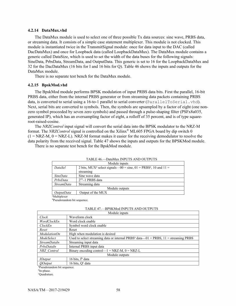
NASA/TM—2017-219429 58
4.2.14 DataMux.vhd
The DataMux module is used to select one of three possible Tx data sources: sine wave, PRBS data, or streaming data. It consists of a simple case statement multiplexer. This module is not clocked. This module is instantiated twice in the TransmitSignal module: once for data input to the DAC (called DacDataMux) and once for Loopback data (called LoopbackDataMux). The DataMux module contains a generic called DataSize, which is used to set the width of the data buses for the following signals: SineData, PrbsData, StreamData, and OutputData. This generic is set to 16 for the LoopbackDataMux and 32 for the DacDataMux (16 bits for I and 16 bits for Q). Table 46 shows the inputs and outputs for the DataMux module.
There is no separate test bench for the DataMux module.
4.2.15 BpskMod.vhd
The BpskMod module performs BPSK modulation of input PRBS data bits. First the parallel, 16-bit PRBS data, either from the internal PRBS generator or from streaming data packets containing PRBS data, is converted to serial using a 16-to-1 parallel to serial converter (ParallelToSerial.vhd). Next, serial bits are converted to symbols. Then, the symbols are upsampled by a factor of eight (one non-zero symbol proceeded by seven zero symbols) and passed through a pulse-shaping filter (PSFx8a035, generated IP), which has an oversampling factor of eight, a rolloff of 35 percent, and is of type square-root-raised-cosine.
The NRZControl input signal will convert the serial data into the BPSK modulator to the NRZ-M format. The NRZControl signal is controlled on the Xilinx® ML605 FPGA board by dip switch 0 (1 = NRZ-M, 0 = NRZ-L). NRZ-M format makes it easier for the receiving demodulator to resolve the data polarity from the received signal. Table 47 shows the inputs and outputs for the BPSKMod module.
There is no separate test bench for the BpskMod module.
TABLE 46.—DataMux INPUTS AND OUTPUTS Module inputs
DataSel 2 bits, MUXa select signals—00 = sine, 01 = PRBSa, 10 and 11 = streaming
SineData Sine wave data PrbsData 223–1 PRBS data StreamData Streaming data
Module outputs OutputData Output of the MUX
aMultiplexer
bPseudorandom bit sequence.
TABLE 47.—BPSKMod INPUTS AND OUTPUTS
Module inputs Clock Waveform clock WordClockEn Word clock enable ClockEn Symbol word clock enable Reset Reset ModulationOn High when modulation is desired ModeSelect Used to select streaming data or internal PRBSa data—01 = PRBS, 11 = streaming PRBS StreamDataIn Streaming input data PrbsDataIn Internal PRBS input data NRZ_Control Binary encoding control—1 = NRZ-M, 0 = NRZ-L
Module outputs IOutput 16 bits, Ib data QOutput 16 bits, Qc data
aPseudorandom bit sequence. bIn-phase. cQuadrature.

NASA/TM—2017-219429 59
4.2.16 ReceiveSignal.vhd
The ReceiveSignal module, shown in Figure 34, takes care of the received data entering the Rx side of the waveform. Incoming data will enter the Rx side from the either the ADC or the Loopback signal. Loopback data is routed directly to a 223–1 bit BERT (PrbsRx23Wrapper) and ADC data is double registered. The module contains a 223–1 PRBS generator to send PRBS data in streaming packets to the GPP independent of the Tx side of the radio.
ReceiveSignal module contains a very simple state machine (shown in Fig. 35) that controls the BERT. When the BERT is enabled (BertEn = ‘1’), the state machine creates a reset signal to the BERT to clear out previous bit and error counts, waits a couple of clock cycles, and then starts the BERT.
The DataInMux process is used to select either LoopbackIn data, AdcDataIn, or PRBS data to go the StreamingInput signal to be used for the Rx-side streaming data source. The RxSourceCtrl input signal selects LoopbackIn when “01”, AdcDataIn when “00”, and PRBS data when “10”.
The ReceiveSignal module is clocked by WFClock signal, which is approximately 200 MHz in the original waveform version. Clock enables are used to provide the required clock rates to different parts of the module. WFClockEn1 is a byte enable, and is used to enable the PrbsRx23 module, which performs BER checking on 8-bit PRBS data bytes. WFClockEn2 is a word (16 bit) enable, and is used for most of the clocking in the ReceiveSignal module. See Sections 4.2.11 and 4.2.12 for details.
Error handling in the ReceiveSignal module consists of passing the error flags from the PrbsRx23_Wrapper up to the STRS_Waveform module to be combined with other error flags into the StatusBits word. Table 48 shows the inputs and outputs for the ReceiveSignal module.
Test bench ReceiveSignal_tb.vhd tests the BERT portion of the module. It contains an instantiated PrbsTx23Wrapper to generate the data to test the ReceiveSignal module. The wave configuration file is ReceiveSignal.wcfg.
Figure 34.—ReceiveSignal module. BERT, bit error rate tester;
MUX, multiplexer; PRBS, pseudorandom bit sequence.

NASA/TM—2017-219429 60
Figure 35.—ReceiveSignal state machine.
TABLE 48.—ReceiveSignal INPUTS AND OUTPUTS Module inputs
WFClock Waveform data clock rate WFClockEn1 Waveform data clock enable WFClockEn2 Waveform data clock enable Reset Reset BertEn BERTa enable RxSourceCtrl 2 bits, Rxb-side data source control AdcDataIn 16 bits, ADCc data LoopbackIn 16 bits, loopback data DataReady High when AdcDataIn is valid FlagReset Resets the error flags
Module outputs SMErrorFlagOut 3 bits, indicates that SMd entered
“others” state DataOut 16 bits, parallel received data SyncLost BERT lost sync SyncLostCnt 8 bits, times synchronization was lost BertBits 64 bits, number of bits received BertErrors 32 bits, number of bit errors counted
aBit error rate tester. bReceive. cAnalog-to-digital converter. dState machine.

NASA/TM—2017-219429 61
4.2.17 PrbsRx23_Wrapper.vhd
The PrbsRx23_Wrapper module is a wrapper module for the PrbsRx23 module. The PrbsRx23 module is 8-bit BERT for a 223–1 length PRBS binary data sequence, but for this implementation, we need parallel PRBS data in 16-bit words. The PrbsRx23_Wrapper extracts two 8-bit bytes from a single 16-bit input data word. To accomplish this, the PrbsRx23 module is enabled at twice the rate of the PrbsRx23_Wrapper module.
This module is clocked by the waveform clock, which is approximately 200 MHz for the original delivered waveform. The 16-bit incoming PRBS data words are clocked by word clock enable, WFClockEn2. Since the BERT takes an 8-bit input word, it must be enabled at twice the rate of the 16-bit word rate, using the byte clock enable, WFClockEn1.
PrbsRx23_Wrapper module uses a very simple state machine (see Fig. 36) to control the order at which the 8-bit bytes (extracted from the 16-bit input data, DataIn) are presented to the PrbsRx23 module.
Error handling in the PrbsRx23_Wrapper module consists of three parts:
(1) A sticky error flag (SMErrorFlagO), which indicates that the PrbsRx23_Wrapper state machine entered the “others” state in the state machine navigation case statement.
(2) Passing up to the next level an error flag, SMErrorFlag, originally from the BERTSyncherSM module, which indicates that the state machine entered the “others” state.
(3) Passing up to the next level the BERTSyncherSM module SyncLost and SyncLossCnt signals.
Figure 36.—PrbsRx23_Wrapper state machine.

NASA/TM—2017-219429 62
TABLE 49.—PrbsRx23_Wrapper INPUTS AND OUTPUTS Module inputs
WFClock Waveform clock WFClockEn1 Byte rate clock enable WFClockEn2 Word rate clock enable Reset Reset Enable Enable signal to start BERTa DataIn 16 bits, input data FlagReset Resets error flags
Module outputs SMErrorFlags 2 bits, indicates that SMb entered “others” state Synched Indicates BERT is synced SyncLost BERT lost sync SyncLostCnt 8 bits, a count of number of times synchronization was lost Bits 64 bits, bits received Errors 32 bits, errors detected
aBit error rate tester. bState machine.
Table 49 shows the inputs and outputs for the PrbsRx23_Wrapper module. Test bench PrbsRx23Wrapper_tb.vhd tests the BERT portion of the module. It reads in 16-bit
PRBS data from a file. Two files are included in the test bench: Prbs23_16bitsWithZeroes.txt, which tests that the BERT will not synchronize to long strings of zeroes, and Prbs23_16bits.txt, which tests the BERT with straight PRBS data. The wave configuration file is PrbsRx23Wrapper.wcfg.
4.2.18 PrbsRx23.vhd
The PrbsRx23 module is 8-bit parallel-input BERT for a 223–1 PRBS sequence. It uses the incoming data to seed the internal PRBS generator. Once the PRBS generator is synced, the PRBS generator runs without the incoming data. The module contains a state machine in BertSyncherSM, which acquires synchronization and detects loss of synchronization. Once synchronized, incoming data is compared to the correct PRBS data to get count of the number of erroneous bits. If synchronization is lost, the BERT will reacquire, but the counts (errors and bits) will not reset and they start up where they left off.
The PrbsRx23 module contains two important processes: PRBS_Gen and CompareProcess. PRBS_Gen generates the PRBS sequence that is used to compare against the incoming data. At the beginning, the incoming data is used to seed the linear feedback shift register (LFSR). Once sync is achieved, the LFSR continues on its own, without incoming data. CompareProcess starts when the PRBS generator is synced to the incoming data. It exclusive ORs (XORs) the incoming data byte (DataIn) to the linear feedback shift register output (Value0) in two separate nibbles and creates an integer (CompareHigh and CompareLow) for each nibble, where each ‘1’ represents a bit error in the data.
The ErrorCounter process is responsible for counting the number of errors in each byte. This process uses a LUT to determine the number of high bits in the CompareHigh and CompareLow signals. The ADDER_LUT simply outputs a 4-bit vector representation of the number of high bits contained in its input signal, CompareHigh or CompareLow. These values are then added together with the running total of errors, as shown in the line of code below:
ErrorCnt <= ErrorCnt + ADDER_LUT(CompareHigh) + ADDER_LUT(CompareLow);
Because the 223–1 PRBS sequence is generated using a linear feedback shift register, it is subject to erroneously synchronizing to long sequences of zeroes. The PrbsRx23 module contains a process, ZeroCounter, which counts the number of consecutive bits that are zero. The ZeroCnt is used as an input the BERTSyncherSM module (see the BERTSyncherSM.vhd section), which will consider a ZeroCnt > 0x3F as a loss of synchronization, resulting in an attempt to resynchronize.

NASA/TM—2017-219429 63
TABLE 50.—PrbsRx23 INPUTS AND OUTPUTS Module inputs
Clock Clock Reset Reset ClockEn Clock enable Enable BERTa enable from BERT enable command DataIn 8 bits, received PRBSb data FlagReset Resets error flags
Module outputs SMErrorFlag SMc error flag Synched Indicates BERT is synced to DataIn SyncLost BERT lost sync SyncLostCnt 8 bits, a count of number of times synchronization was lost Bits 64 bits, number of bits received Errors 32 bits, number of errors counter
aBit error rate tester. bPseudorandom bit sequence. cState machine.
This module is clocked by the waveform clock and enabled by the byte clock enable, WFClockEn2. Error handling in the PrbsRx23 module consists of passing an error flag, SMErrorFlag, from the
BERTSyncherSM module, which indicates that the state machine entered the “others” state in the state machine navigation case statement, up to the next level. The PrbsRx23 module also passes a SyncLost signal and SyncLossCnt signal up to the next level to become part of the status bits along with the other error flags. Table 50 shows the inputs and outputs for the PrbsRx23 module.
Test bench PrbsRx23_tb.vhd tests this module. It reads in 8-bit PRBS data from a text file. Multiple text files are included to test with and without errors. These are defined in the test bench comments. The wave configuration file is PrbsRx23.wcfg.
4.2.19 BertSyncherSM.vhd
The BertSyncherSM module works with signals that come from the PrbsRx23 module, contains a state machine that controls synchronization of the BERT to the incoming data, and detects loss of synchronization. The state machine (diagram is shown in Fig. 37) starts when the BERT is enabled (Enable = 1) and navigates to the SYNCHING state after a one cycle wait state. In the SYNCHING state, the module input DataIn is compared to the module input Value0 (the LFSR output) for a window of 10 bytes (SYNC_BYTES). If there are no errors during that 10-byte window and there have not been 24 or more consecutive zeroes in the data, the BERT is considered synchronized and the state machine moves to the DATASYCNHED state. If 24 or more consecutive zeroes in the data are detected in the 10-byte window, the state machine will move to the IDLE state to start over.
In the DATASYNCHED state, the number of errors (ErrorCnt) in the received data is counted during a window of 32 data bytes. The number of consecutive zeroes in the incoming data is also counted. If there are 63 or more consecutive zeroes in the 32-byte window (256 bits), then the BERT had synchronized to all zeroes instead of the 223–1 PRBS sequence. This is considered a loss of synchronization and the state machine goes to the SYNC_LOST state.
When the 32-byte window is completed and there was no false lock to all zeroes, the state machine will go to the CHECK4ERRORS state. In CHECK4ERRORS, synchronization is lost if there are greater than 32 bit errors in the 32-byte window. The state machine will go to the SYNC_LOST state where the SyncLost signal in asserted and the SyncLossCnt is incremented, and then return to the IDLE state to attempt to resynchronize.
This module is clocked by the waveform clock and enabled by the word clock enable, WFClockEn2.

NASA/TM—2017-219429 64
Figure 37.—BERTSyncherSM state machine.
Error handling in the BertSyncherSM module consists of three parts: (1) A sticky error flag (SMErrorFlag), which indicates that the BertSyncherSM state machine
entered the “others” state in the state machine navigation case statement. (2) A “sticky” SyncLost signal, which indicates that the BERT lost synchronization with the
incoming PRBS data. (3) SyncLossCnt, which is an 8-bit signal that keeps track of the number of total losses of
synchronization.
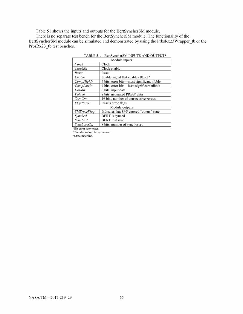
NASA/TM—2017-219429 65
Table 51 shows the inputs and outputs for the BertSyncherSM module. There is no separate test bench for the BertSyncherSM module. The functionality of the
BertSyncherSM module can be simulated and demonstrated by using the PrbsRx23Wrapper_tb or the PrbsRx23_tb test benches.
TABLE 51.—BertSyncherSM INPUTS AND OUTPUTS
Module inputs Clock Clock ClockEn Clock enable Reset Reset Enable Enable signal that enables BERTa CompHighIn 4 bits, error bits—most significant nibble CompLowIn 4 bits, error bits—least significant nibble DataIn 8 bits, input data Value0 8 bits, generated PRBSb data ZeroCnt 16 bits, number of consecutive zeroes FlagReset Resets error flags
Module outputs SMErrorFlag Indicates that SMc entered “others” state Synched BERT is synced SyncLost BERT lost sync SyncLossCnt 8 bits, number of sync losses
aBit error rate tester. bPseudorandom bit sequence. cState machine.

NASA/TM—2017-219429 66
4.3 STRS_Radio_Pkg
STRS_Radio_Pkg is a VHDL package that is used to share objects among many of the design modules in this implementation. This package contains a number of reusable constants and defines the Xilinx® ChipScope™ Pro Integrated CONtroller (ICON) and Integrated Logic Analyzer (ILA) components so they can be used in multiple modules (Table 52). The package also contains the LUT used in PrbsRx23.vhd to add up the number of errors in a received byte.
TABLE 52.—DEFINITION OF CONSTANTS IN STRS_Radio_Pkg Constant name Value Description Modules
PACKET_SIZE 60 Length of a command response packet
EthernetRx, TxResponsePackets, RespFifoInputSM, RespFifoOutputSM
DATA_PACKET_SIZE 557 Length of a streaming data packet
EthernetRx, CreatePacketSM, RxStreamingData, and as BYTECNT in StrDataFifoOutputSM
HEADER_SIZE 42 Length of a transmit header
RespFifoInputSM and CreatePacketSM
SOURCE_PORT_BYTE 33 Location of source port number in packet header
EthernetRx
REMAINING_HEADER_SIZE 26 Length of remainder of header in Txa-side packets after enable goes high
RxPackets
COMMAND_RESPONSE_SIZE 120 Length of a command response packet payload
OutputDataMux and TxResponsePackets
STREAM_PKT_BYTE1 0x8C Tx-side streaming UDPb packet source port address—MSBc
EthernetRx
STREAM_PKT_BYTE2 0xA0 Tx-side streaming UDP packet source port address—LSBd
EthernetRx
CMD_PKT_BYTE1 0x8C Command UDP packet source port address—MSB
EthernetRx
CMD_PKT_BYTE2 0x35 Command UDP packet source port address—LSB
EthernetRx
PACKET_BYTE_CNT 570 Number of bytes in an Rx-sidee streaming data packet
RxStreamingData
WAIT_CNT 500 Number of clock cycles between Rx-side streaming data packets
RxStreamingData
PACKET_NUM_CNT 4 Number of data packets sent in a group of packets
RxStreamingData
aTransmit. bUser Datagram Protocol. cMost significant bit. dLeast significant bit. eReceive-side.

NASA/TM—2017-219429 67
TABLE 53.—FIELD-PROGRAMMABLE GATE ARRAY (FPGA) RESOURCE UTILIZATION Resource name Usage (percentage) Usage (used/available)
Slice registers 2 percent 6,717/301,440 Slice LUTsa 4 percent 7,264/150,720
Fully used LUT–FF pairs 49 percent 4,314/9,211
Bonded IOBsb 17 percent 103/600 DSP48E1s 2 percent 22/768 Block RAMc/FIFOd 40 percent 169/416 BUFG/BUFGCTRLs 32 percent 14/32
aLookup tables. bInput/output blocks. cRandom-access memory. dFirst in first out.
4.4 Programmable Logic Device (PLD) Resource Usage
The amount of PLD resources utilized in the design is shown in Table 53.
5.0 Simulation and Testing
Much of the iPAS STRS radio FPGA design was thoroughly simulated using test benches and the Xilinx® ISE simulator (iSIM). Information about test benches is included with each module description in Section 4.0 of this document. Simulation was used during development to test and debug the VHDL code implementation. Further testing of the FPGA code occurred in the FPGA by using a C++ test program to emulate the functions of the GPM. Formal verification of the design was completed with full system testing.
6.0 Conclusions
The Space Telecommunications Radio System (STRS) was developed to reduce the cost and risk of using complex, configurable, and reprogrammable radio systems across multiple NASA missions. To promote the use of the STRS architecture for future NASA advanced exploration missions, NASA Glenn Research Center developed an STRS-compliant software defined radio (SDR) on a radio platform used by the Advanced Exploration System program at the NASA Johnson Space Center in their Integrated Power, Avionics, and Software (iPAS) laboratory. This platform, called the Reconfigurable, Intelligently-Adaptive Communication System (RIACS) platform, consists of easily obtainable commercial off-the-shelf hardware. The hardware description language (HDL) code developed for the field-programmable gate array (FPGA) portion of the platform consists of a wrapper and a test waveform. The wrapper implements each platform interface that is accessible to the FPGA for SDR waveform development. The test waveform is a placeholder for a full radio waveform, and it exercises and demonstrates each interface in the FPGA wrapper. A waveform developer can remove the test waveform and replace it with a new waveform to create a custom radio on the platform. The result of this development is a very low cost STRS-compliant platform that can be used for waveform developments for multiple applications.


NASA/TM—2017-219429 69
Appendix
The following abbreviations and acronyms are used within this document. ADC analog-to-digital converter API application programming interface BER bit error rate BERT bit error rate tester BPSK binary phase shift keying DAC digital-to-analog converter DSP digital signal processor EDK Embedded Development Kit EMAC Ethernet Media Access Controller FDI firmware developer interface FIFO first in first out FMC FPGA Mezzanine Card FPGA field-programmable gate array GPM general purpose module GPP general purpose processor GUI graphical user interface HAL hardware abstraction layer HDL hardware description language HID hardware interface description I in-phase ICON Integrated CONtroller ID identification IDDR input dual data rate IHL Internet header length IIC Inter-Integrated Circuit ILA Integrated Logic Analyzer IOB input/output block IP Internet Protocol iPAS Integrated Power, Avionics, and Software ISE Integrated Synthesis Environment iSIM ISE Simulator LED light-emitting diode LFSR linear feedback shift register LSB least significant bit/byte LUT lookup table MAC media access control MSB most significant bit/byte MUX multiplexer ODDR output dual data rate OE operating environment PC personal computer PHY physical layer PLD programmable logic device PLL phase-locked loop PRBS pseudorandom bit sequence Q quadrature-phase RAM random-access memory

NASA/TM—2017-219429 70
RIACS Reconfigurable, Intelligently-Adaptive Communication System RF radiofrequency RFM RF module ROM read-only memory Rx receive SCaN Space Communications and Networking SDK Software Development Kit SDR software defined radio SM state machine SPM signal processing module STRS Space Telecommunications Radio System SW switch Tx transmit UART universal asynchronous receiver/transmitter UDP User Datagram Protocol VGA variable-gain amplifier VHDL VHSIC Hardware Description Language WF waveform XOR exclusive or

NASA/TM—2017-219429 71
References
1. Shalkhauser, Mary Jo W.; and Roche, Rigoberto: Hardware Interface Description for the iPAS STRS Radio. NASA/TM—2017-219432, to be published, 2017.
2. Virtex-6 FPGA Embedded Tri-Mode Ethernet MAC Wrapper v1.4 Getting Started Guide. https://www.xilinx.com/support/documentation/ip_documentation/v6_emac_gsg545.pdf Accessed April 21, 2017