Embed Size (px)
Citation preview

ProgrammableProgrammable LogicLogic DesignDesign
Grzegorz BudzyGrzegorz Budzyńń
LLectureecture 1:1:IntroductionIntroduction

Plan
• Workplan for the semester
• Introduction
• PLA structures
• PLD structures
• CPLD structures

Introduction
• What is this course about
• What is the aim of this course

Course requirements
• Course consists of:
– Lecture – 2h/week
– Laboratory – 2h/week
• Course ends with an exam
• Course completion requires passing
laboratory class and the exam
• The exam will be held during examination
period

Workplan for the semster
• Lecture 1
– Basic definitions. PLD, PLA and CPLD structures
• Lecture 2
– Review of FPGA and ASIC structures
• Lecture 3
– FPGA - programming environment

Workplan for the semster
• Lecture 4
– Introduction to VHDL
• Lecture 5
– Introduction to VHDL – statements
• Lecture 6
– Combinational circuits

Workplan for the semster• Lecture 7
– Sequential circuits part 1
• Lecture 8
– Sequential circuits part 2
• Lecture 9
– FPGA clocking schemes
• Lecture 10
– Clock management technology

Workplan for the semster• Lecture 11
– Microcontroller cores in FPGA
• Lecture 12
– VHDL vs Verilog
• Lecture 13,14
– CPLD and FPGA market view
• Lecture 15
– Advanced hardware in FPGA structures

• Lecture 1
Classic logic vs programmble logic.
Basic definitions.
PLD, PLA and CPLD
Programmable logic vs processors

Classic logic vs programmble logic

Classic logic – AND gate

Classic logic– OR gate

Classic logic– XOR gate

Classic logic– XNOR gate

Classic logic– ICs

„Classic” design process
• Define problem
• Define logical equations
• Minimize equations with Karanugh table
• Build electronic circuit with logic gates (logic
ICs)

„New” design process
• Define problem
• Define proper algorithm
• Describe algorithm in a HDL (hardware
description language)
• Build electronic circuit with PLD device

Karanugh table

Basic definitions
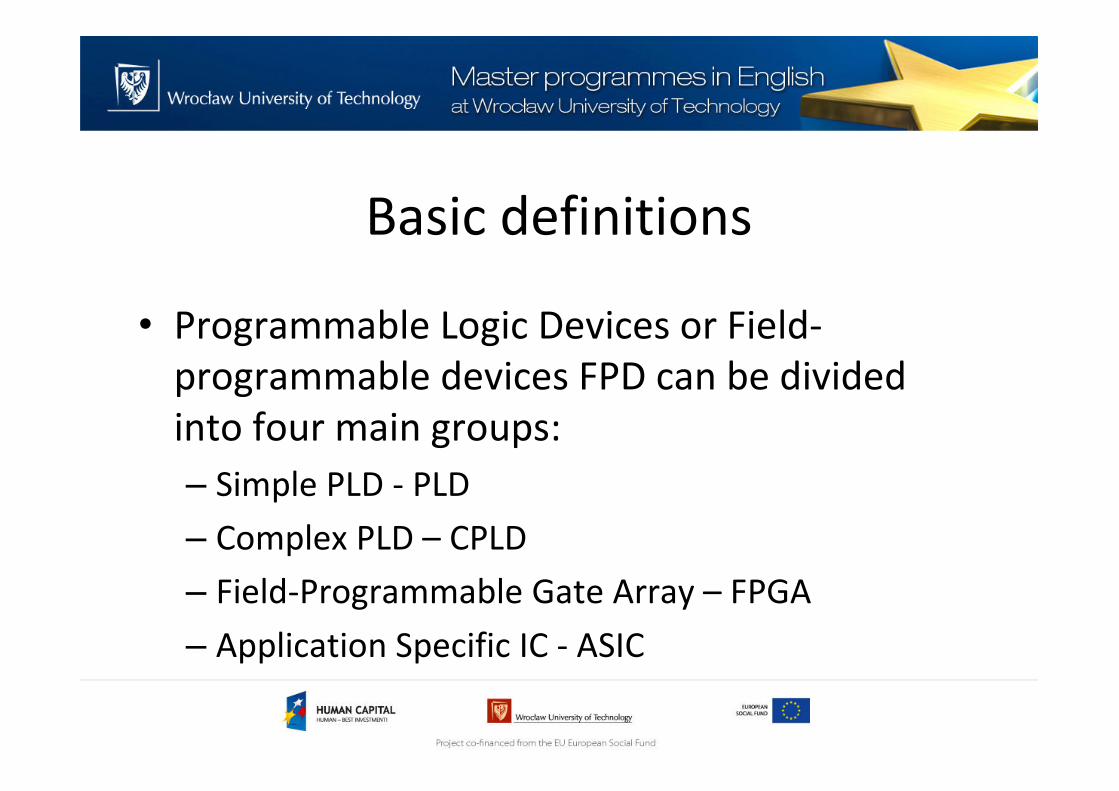
Basic definitions
• Programmable Logic Devices or Field-
programmable devices FPD can be divided
into four main groups:
– Simple PLD - PLD
– Complex PLD – CPLD
– Field-Programmable Gate Array – FPGA
– Application Specific IC - ASIC

Basic definitions

Basic definitions• The market for FPDs has grown dramatically
over the past time to the point where there isnow a wide assortment of devices to choose from
• The most compelling advantages of FPDs are:
– instant manufacturing turnaround
– low start-up costs
– low financial risk
– ease of design changes

SPLD - PLD
• PLD — a Programmable Logic Device (PLD) is a relatively small
FPD that has only a programmable AND-plane

SPLD - PAL
• PAL — a Programmable Array Logic (PAL) is a relatively small
FPD that has a programmable AND-plane followed by a fixed
OR-plane

PAL structure• PLA were expensive to produce
• That is why a simplified PAL structure was introduced
• PALs feature only a single level of programmability, consisting of a programmable “wired” AND plane that feeds fixed OR-gates
• PALs usually contain flip-flops connected to the OR-gate outputs so that sequential circuits can be realized

SPLD - PLA
• PLA — a Programmable Logic Array (PLA) is a relatively small
FPD that contains two levels of logic, an AND-plane and an OR-
plane, where both levels are programmable

PLA structure
• PLA consists of two levels of logic gates: a
programmable “wired” AND-plane followed
by a programmable “wired” OR-plane
• Any of its inputs (or their complements) can
be AND’ed together in the AND-plane
• Each AND-plane output can thus correspond
to any product term of the inputs

PLA structure
• Each OR plane output can be configured to
produce the logical sum of any of the AND-
plane outputs
• PLAs are well-suited for implementing logic
functions in sum-of-products form
• PLA are quite versatile, since both the AND
terms and OR terms can have many inputs

GAL structure
• GAL (Generic Logic Array) was an innovation
of the PAL and was invented by Lattice
Semiconductor
• Its primary benefit was that it was eraseable
and re-programmable making prototyping and
design changes easier for engineers

CPLD structure
• As technology has advanced, it has become possible to produce devices with higher capacity than PALs and PLAs
• The only feasible way to provide large capacity devices based on SPLD architectures is to integrate multiple SPLDs onto a single chip and provide interconnect to programmably connect the SPLD blocks together – that is how CPLD comes up

CPLD

CPLD structure• CPLD is between PAL and FPGA
• With PAL it has in common:
– It starts immediately (no ext ROM required)
– In some devices routing constrains most logic blocks to have input and output signals connected to external pins
• With FPGA it has in common:
– Large number of gates available
– Some provisions for logic more flexible than sum-of-product expressions

CPLD - Applications
• CPLDs are useful for a very wide assortment of applications, e.g.:
– implementing random glue logic
– prototyping small gate arrays
– resonably complex designs:
• graphics controller
• UART
• LAN controller
• Cache control

FPGA features
• FPGAs comprise an array of uncommitted
circuit elements, called logic blocks, and
interconnect resources
• FPGAs configuration is performed through
programming by the end user
• FPGAs have been responsible for a major shift
in the way digital circuits are designed

FPGA features
• The FPGA differs from the CPLD in that,
instead of solving the logic design by
interconnecting logic gates, it uses a look-up
table (LUT) method to resolve the particular
logic requirement.
• This allows PLD manufacturers to form a more
streamlined design, creating a much denser
and faster PLD

FPGA block diagram
Sourc
e: [1
]
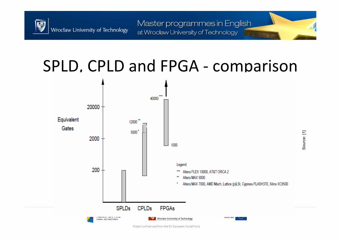
SPLD, CPLD and FPGA - comparison
Sourc
e: [1
]

SPLD, CPLD and FPGA - comparison
Sourc
e: [1
]

Programmable logic vs processors

Logic vs MicrocontrollerMicrocontroller:
– Easy to program, excellent for control and state machine applications
– Resource requirements remain constant with increasing complexity
– Excellent for lower-performance functions
– Executes sequentially
– Performance degrades with complexity increase
– Program memory requirements increase with complexity increase
– Slower response to simultaneous inputs

Logic vs MicrocontrollerFPGA:
– Significantly higher performance
– Excellent at parallel operations
– Sequential vs. parallel implementation tradeoffsoptimize performance or cost
– Fast response to multiple, simultaneous inputs
– Control and state machine applications more difficult to program
– Logic resources grow with complexity increase

Thank you for your attention

References
[1] Brown S., Rose J., „Architecture of FPGAs and CPLDs: A
Tutorial”
[2] Kelitz W., „Digital Electronics – a practical approach with
VHDL”
[3] http://www.ece.rice.edu/~kmram/elec326/Notes/notes-
326-set5.pdf
![Applied Wireless Electronics Grzegorz Budzy ń Lecture 3 ... · PDF fileApplied Wireless Electronics Grzegorz Budzy ... ZigBee – Frequency range Source: [2] ... Message Integrity](https://img.dokumen.tips/doc/110x75/5ab819af7f8b9ac1058c4907/applied-wireless-electronics-grzegorz-budzy-n-lecture-3-wireless-electronics.jpg)