Embed Size (px)
Citation preview

New Methodology for Spiral Inductor Design
Albert Yen
UMC

Outline
n Introductionn Inductor Library from Foundryn Customer Request on Inductorn EM Design Methodology for Inductorn Results and Comparisonn Other Application using EMDMn Conclusion
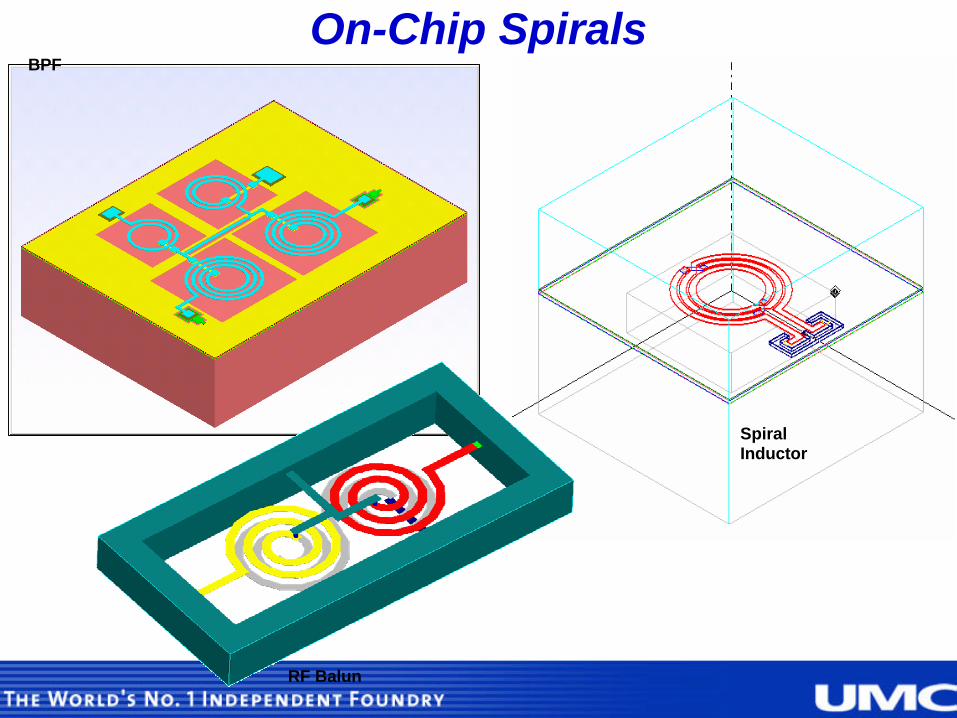
On-Chip Spirals
RF Balun
BPF
Spiral Inductor

Ideal Circular Inductor
D
D+W
+S
W
S
N=4.5GND
Diffusion Dummy Block
Metal 5 Metal 6
Port1 Port2D
D+W
+S
W
S
N=4.5GND
Diffusion Dummy Block
Metal 5 Metal 6
Port1 Port2
Geometrical Parameter
Diameter
Number of Turn
Width of Trace
Space between Trace

Inductor Equivalent Model
Ls
Cp
Port1 Port2
Rs
Cox1 Cox2
Rsub1 Rsub2Csub1 Csub2

Spiral in CMOSn Sheet resistance of metal layer can be used only for
calculating the DC resistance of the spiral.n Due to the skin effect, eddy current and “current
crowding”, the resistance of the spiral increases at high frequency.
n Copper metal and thick top-level metal to improve the maximum inductor Q.
n Multiple levels of metal strapped together to create a spiral with a lower dc resistance.
n PGS: pattern ground shield reduce the substrate lossn CMOS substrate losses still the limiting factor

Outline
n Introductionn Inductor Library from Foundryn Customer Request on Inductorn Inductor Design Methodology {EMDM}n Results and Comparisonn Other Application using EMDMn Conclusion

Foundry’s Inductor Model and Library
n Empirical formulan Direct measured inductor libraryn Scalable model inductor library

Empirical Formula
OD
davg
dtrace
Wavg
trace
dd
=ρ

Empirical Formula
n : number of turns.
µ : permeability of free space
davg: average diameter
: percentage of the inductor area that is filled by metal traces.
++
= 2
2
125.0178.0067.2
ln2
ρρρπ
µ avgdnL
ρ
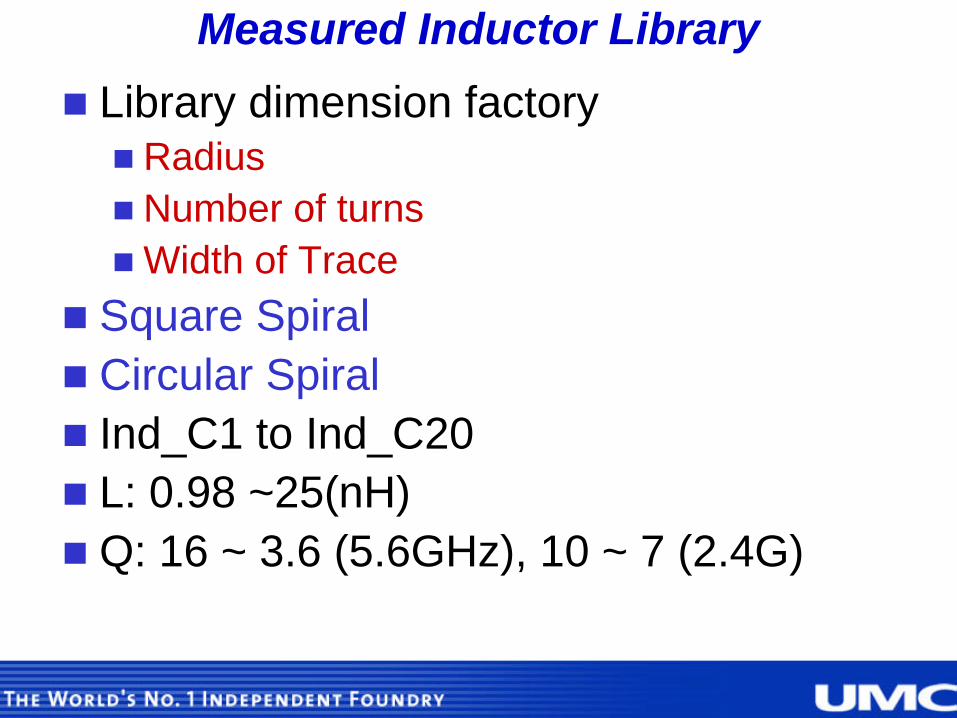
Measured Inductor Library
n Library dimension factorynRadiusnNumber of turnsnWidth of Trace
n Square Spiraln Circular Spiraln Ind_C1 to Ind_C20n L: 0.98 ~25(nH)n Q: 16 ~ 3.6 (5.6GHz), 10 ~ 7 (2.4G)

Scalable Inductance v.s. radius

Scalable Inductance v.s. turns

Outline
n Introductionn Inductor Library from Foundryn Customer Request on Inductorn Inductor Design Methodology {EMDM}n Results and Comparisonn Other Application using EMDMn Conclusion

Various Spiral
?

Differential Spiral
?

Balance Spiral

Stack Balance Spiral

More Inductor Lib?
n Shape: Square, Octagonal Inductor, Circular Inductor
n Single end or Balance Inductor
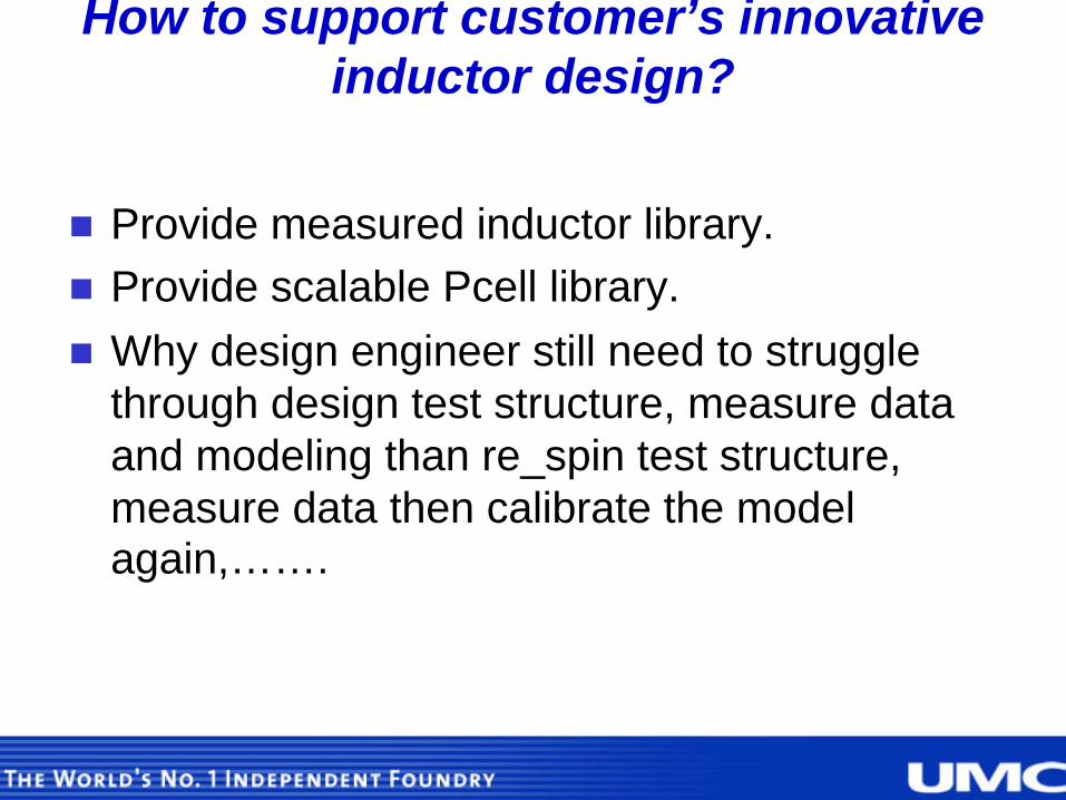
How to support customer’s innovative inductor design?
n Provide measured inductor library.n Provide scalable Pcell library.n Why design engineer still need to struggle
through design test structure, measure data and modeling than re_spin test structure, measure data then calibrate the model again,…….
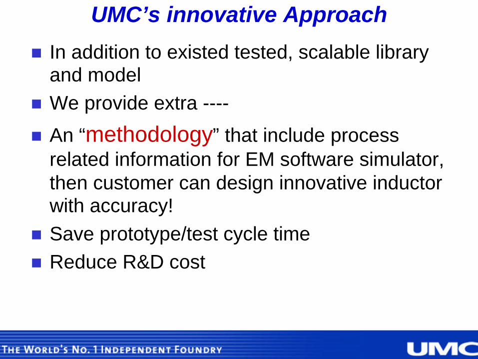
UMC’s innovative Approach
n In addition to existed tested, scalable library and model
n We provide extra ----
n An “methodology” that include process related information for EM software simulator, then customer can design innovative inductor with accuracy!
n Save prototype/test cycle timen Reduce R&D cost

Ansoft HFSS
n Current Version 9.0
n A true 3D Electromagnetic-Based Design Tool
n Widely used in Package, Wave guide and Antenna
n UMC is the first Foundry that provide the methodology for using 3D EM design tool to support RFIC design

UMC’s New Approach (1) - What is Our Purpose?
ØGeneral Inductor Design
With Si measurement data
3-D EM simulation data
+ RF SPICE model
3-D EM simulation interpolation for S parameter
3-D EM simulation extrapolation for S parameter Parameter 1
Param
eter 2
Inductor Pool
Parameters : Xo; W; S & N

Ø Special Inductor Design
Novel Inductor Design 3-D EM simulation S-Parameter Designer
Pattern shielding ground Transformer or stacked or others
UMC’s New Approach (2) - What is Our Purpose?

UMC’s New Approach (3)
Technology profile
SiO2 ε
Si
M1M22
M3
Testkey Layout
3-D EM Simulation Circuit SimulationS-Parameter
WaferFabrication
ICCAP
Model
ExtractionUMC Process
Work Flow
RF SPICEModel
Ansoft HFSSAnsoft HFSS
Ansoft Designer

UMC’s New Approach (4)- What is Technology File?
Silicon Thickness
M5 Thickness
SiO2 Thickness
M6 Thickness
Passivation Thickness
εrConductivity
εr
εr
Top Metal
Second Top Metal
εr
SiO2 Thickness
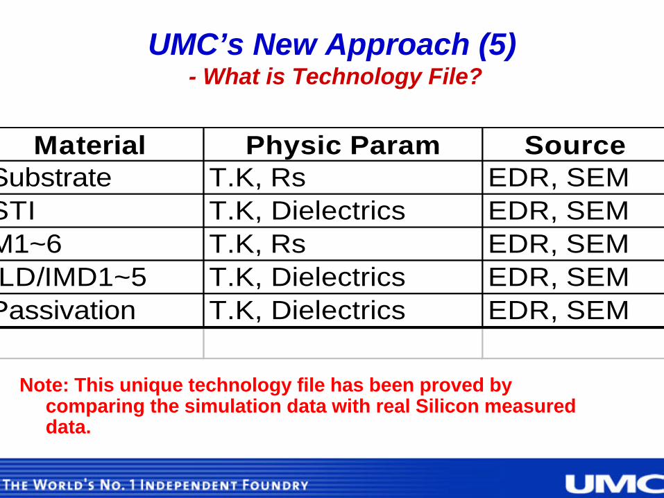
UMC’s New Approach (5)- What is Technology File?
Note: This unique technology file has been proved by comparing the simulation data with real Silicon measured data.
Material Physic Param SourceSubstrate T.K, Rs EDR, SEMSTI T.K, Dielectrics EDR, SEM M1~6 T.K, Rs EDR, SEM ILD/IMD1~5 T.K, Dielectrics EDR, SEMPassivation T.K, Dielectrics EDR, SEM

Ansoft HFSS: Spiral Inductor Macros

EMDM Inductor Design Flow
Only need to input design parameter:N TurnsW WidthS SpacingT Top Metal thicknessThen chose: Segments, Hextangle , Octangle, Circular

Operation Interface
n It is friendly to user that just only key in inductor’s parameter;Overall Dimension, Width, Spacing, Turns & Thickness

Current Status
n Success develop an unique technology file to represent UMC’s process used in Ansoft HFSS EM simulation.
n Process: 0.18um Logic 1P6M process with 20KA and 30kA Al top thick Metal.
n Valid Frequency Range: Simulation & Measurement sweep frequency: 0.6GHz~20.6GHz

Current Status
Ø For general Inductor design, both real Silicon measurement data and 3-D simulation data are used in the model extraction.
Ø Combining these two groups of raw data, we can extract RF SPICE model with higher accuracy.
ØThe technology file used in here can be faithfully represents Silicon process parameter.
Ø Based on the calibrated technology file, designers can implement novel idea, then obtain S-parameter for circuit simulation.

Outline
n Introductionn Inductor Library from Foundryn Customer Request on Inductorn Inductor Design Methodology {EMDM}n Results and Comparisonn Other Application using EMDMn Conclusion
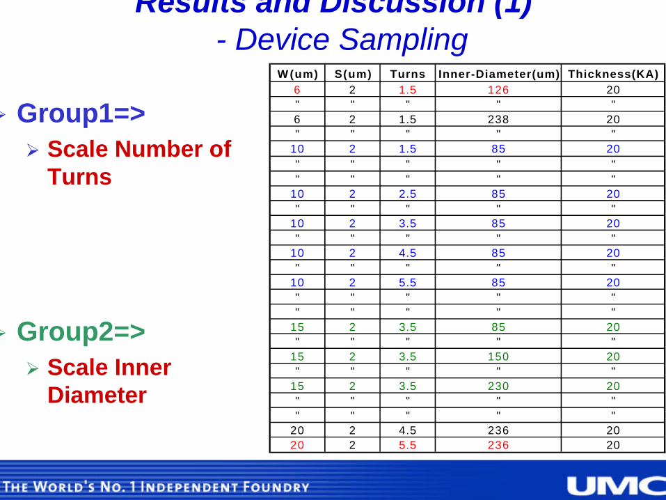
W (um) S(um) Turns Inner-Diameter(um) Thickness(KA)6 2 1.5 126 20" " " " "6 2 1.5 238 20" " " " "
10 2 1.5 85 20" " " " "" " " " "
10 2 2.5 85 20" " " " "
10 2 3.5 85 20" " " " "
10 2 4.5 85 20" " " " "
10 2 5.5 85 20" " " " "" " " " "
15 2 3.5 85 20" " " " "
15 2 3.5 150 20" " " " "
15 2 3.5 230 20" " " " "" " " " "
20 2 4.5 236 2020 2 5.5 236 20
Results and Discussion (1)- Device Sampling
Ø Group1=> Ø Scale Number of
Turns
Ø Group2=> Ø Scale Inner
Diameter

Results and Discussion (2)- Inductor Simulation Profile
Port2
Port1
Ø 3-D design environment, substrate effect can be included.
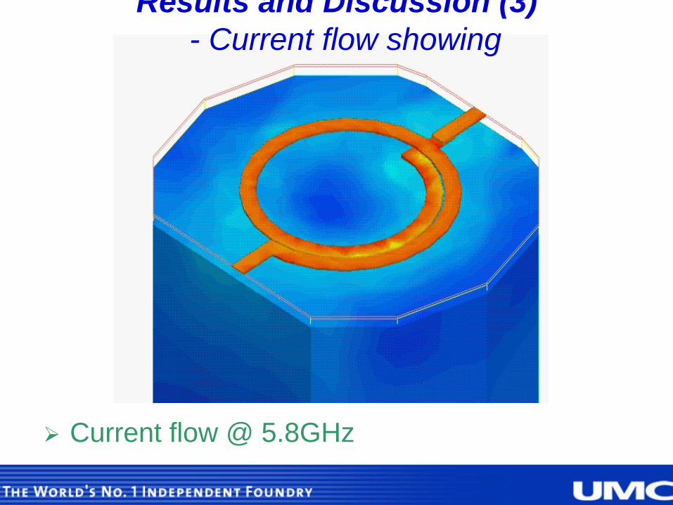
Results and Discussion (3)- Current flow showing
Ø Current flow @ 5.8GHz

Results and Discussion (4) - E&M field showing
Mag of Electric field @ 5.8GHz Mag of Magnetic field @ 5.8GHz

Results and Discussion (5) - E&M field showing
Vector of Electric field @ 5.8GHz
Vector of Magnetic field @ 5.8GHz

0.18-micro 1P6M Inductor N=5.5 comparison
-4
-2
0
2
4
6
8
10
0 1 10 100Frequency[GHz]
Qu
alit
y F
acto
r
0
2
4
6
8
10
12
14
Ind
uct
ance
[nH
]
N5.5_s_QN5.5_m_QN5.5_s_LN5.5_m_L
Results and Discussion (6)- L/Q simulation&measurement
comparison
Ø Width=10µm, Spacing=2µm, Di= 85µm, Turns=5.5, Al=20KA

0.18-micro 1P6M Inductor N=4.5 comparison
-4
-2
0
2
4
6
8
10
0 1 10 100Frequency[GHz]
Qu
alit
y F
acto
r
0
2
4
6
8
10
12
14
Ind
uct
ance
[nH
]
N4.5_s_Q
N4.5_m_Q
N4.5_s_L
N4.5_m_L
Ø Width=10µm, Spacing=2µm, Di= 85µm, Turns=4.5, Al=20KA
Results and Discussion (7)- L/Q comparison

0.18-micro 1P6M Inductor N=3.5 comparison
-2
0
2
4
6
8
10
12
14
0 1 10 100Frequency[GHz]
Qu
alit
y F
acto
r
0
1
2
3
4
5
6
7
8
Ind
uct
ance
[nH
]
N3.5_s_Q
N3.5_m_Q
N3.5_s_L
N3.5_m_L
Ø Width=10µm, Spacing=2µm, Di= 85µm, Turns=3.5, Al=20KA
Results and Discussion (8)- L/Q comparison

0.18-micro 1P6M Inductor N=2.5 comparison
0
2
4
6
8
10
12
14
16
0 1 10 100Frequency[GHz]
Qu
alit
y F
acto
r
0
1
2
3
4
5
6
7
8
Ind
uct
ance
[nH
]
N2.5_s_Q
N2.5_m_Q
N2.5_s_L
N2.5_m_L
Ø Width=10µm, Spacing=2µm, Di= 85µm, Turns=2.5, Al=20KA
Results and Discussion (9)- L/Q comparison

0.18-micro 1P6M Inductor N=1.5 comparison
0
3
6
9
12
15
18
21
24
0 1 10 100Frequency[GHz]
Qu
alit
y F
acto
r
0
1
2
3
4
5
6
7
8
Ind
uct
ance
[nH
]
N1.5_s_Q
N1.5_m_QN1.5_s_L
N1.5_m_L
Ø Width=10µm, Spacing=2µm, Di= 85µm, Turns=1.5, Al=20KA
Results and Discussion (10)- L/Q comparison

0.18-micro 1P6M Inductance/diff diametercomparison
-1
0
1
2
3
45
6
7
8
9
10
0 1 10 100Frequency[GHz]
Ind
uct
ance
[nH
]
D150_s_LD 85_s_LD150_m_LD 85_m_LD230_s_LD230_m_L
Results and Discussion (11) - Simulation & Measurement comparison
Ø Fixed width=15µm, spacing=2µm, Turns=2.5 & Al=20KA, variable Di: 85µm, 150µm and 230µm
Ø Good agreement with inductance.

0.18-micro 1P6M Inductor Case1 comparison
-4
-2
0
2
4
6
8
10
12
14
0 1 10 100Frequency[GHz]
Qua
lity
Fact
or
1
2
3
4
5
6
7
8
9
10
Indu
ctan
ce[n
H]
Q_simulation
Q_measurement
L_simulationL_measurement
Results and Discussion (12) - Inductance & Q-value Comparison - (Case1)
Ø Simulation: Qmax = 10.35 @ 4GHz, Fsr=14.2GHz.Ø Measurement: Qmax = 10.8 @ 3.8GHz, Fsr=14GHz.
W:15um, S:2um, D:202um, N:2p5, AL:30K

0.18-micro 1P6M Inductor Case2 comparison
-6
-4
-2
0
2
4
6
8
10
12
0 1 10 100Frequency[GHz]
Qua
lity
Fact
or
3
6
9
12
15
18
21
24
27
30
Indu
ctan
ce[n
H]
Q_simulationQ_measurement
L_simulationL_measurement
Ø Simulation: Qmax = 8.57 @ 1.4GHz, Fsr=6.2GHz.Ø Measurement: Qmax = 8.1 @ 1.4GHz, Fsr=6.4GHz.
Results and Discussion (13) - Inductance & Q-value Comparison (Case2)
- W: 6um, S:2um, D:210um, N:5p5, AL:30K

Results and Discussion (14) - Deep-trench pattern--case3
Ø Use Deep-trench to reduce substrate loss.Ø Deep-trench Side Cross Section.

Results and Discussion (15) - Deep-trench pattern--case3
0.18-micro 1P6M Inductor with Deeptrenchcomparison
-4
-2
0
2
4
6
8
10
12
14
16
0 1 10 100Frequency[GHz]
Qu
alit
y F
acto
r
0
1
2
3
4
5
6
7
8
9
10
Ind
uct
ance
[nH
]
DT_s_Q
DT_m_Q
DT_s_L
DT_m_L

Outline
n Introductionn Inductor Library from Foundryn Customer Request on Inductorn Inductor Design Methodology {EMDM}n Results and Comparisonn Other Application using EMDMn Conclusion

EMDM Flow
Ansoft HFSSwith Optimetrics
AnsoftLinks
Macros
DXF
ACIS
GDSII
Ansoft Designer
Virtuoso
Matrix ParametersS-, Y-, Z-
Results:Inductance
Quality FactorSelf-Resonance
etc
UMC Technology
File
PowerPlugin

AnsoftLink for Virtuoso
Easier than
Cut & Paste

Other Use of HFSS in IC design
n With UMC EMDM:n Model extraction on Interconnectionn Cross Talk analysis in RF or High Speed Digital ICn Capacitor: MIM, MOM (fringing)n Package Modeling for the IC Designn Internal Antenna Designn EM analysis RFIC with PCB

Outline
n Introductionn Inductor Library from Foundryn Customer Request on Inductorn Inductor Design Methodology {EMDM}n Results and Comparisonn Other Application using EMDMn Conclusion

Conclusion
n Customer’s success is always our first goaln The RF design support is enhanced by providing an
accurate, efficient methodology for inductor library development.
n EMDM can be extended to use in much general high frequency analysis base on the same unique tech file.
n Reduce develop cycle time and cost, customer can go into production much faster.
n UMC is always seeking a better, improved service for our customer

Inductor Top View
Please Fill Out the Survey Questionnaires