Embed Size (px)
Citation preview

This document is owned by Agilent Technologies, but is no longer kept current and may contain obsolete or
inaccurate references. We regret any inconvenience this may cause. For the latest information on Agilent’s
line of EEsof electronic design automation (EDA) products and services, please go to:
www.agilent.com/fi nd/eesof
Agilent EEsof EDA

Agilent EEsof RFIC SeminarSpring 2004
Accurate Modeling of SpiralInductors on Silicon FromWithin Cadence Virtuoso usingPlanar EM Simulation

Spiral Inductor Design on Si with RFDE Momentum2004
Page 2
Overview
Spiral Inductor Models Availability & LimitationsMomentum Technology OverviewKey Physical Effects Considered in MomentumRFDE Momentum Solution ProcessMomentum Application BenchmarkSummary
Spiral Inductor Design on Si with RFDE Momentum2004
Page 3
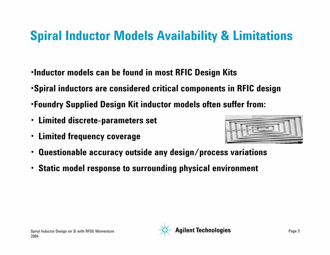
Spiral Inductor Models Availability & Limitations
•Inductor models can be found in most RFIC Design Kits•Spiral inductors are considered critical components in RFIC design•Foundry Supplied Design Kit inductor models often suffer from:• Limited discrete-parameters set• Limited frequency coverage• Questionable accuracy outside any design/process variations• Static model response to surrounding physical environment

Spiral Inductor Design on Si with RFDE Momentum2004
Page 4
Traditional Characterization MethodMeasurement-based Modeling ApproachFabricate a large number of discretely varying topologiesPositives: Good accuracy over predefined frequency range and
discrete parameters’ samplesNegatives: Need to fabricate test wafer(s): Very time consuming and
costly Limited discrete-parameter set hindering design options Static lumped-element models unresponsive to
component’s physical surroundings Need component modeling skills Any updates to existing models can be just as costly as
starting a new model
Spiral Inductor Design on Si with RFDE Momentum2004
Page 5
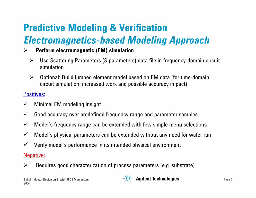
Predictive Modeling & VerificationElectromagnetics-based Modeling Approach Perform electromagnetic (EM) simulation
Use Scattering Parameters (S-parameters) data file in frequency-domain circuitsimulation
Optional: Build lumped element model based on EM data (for time-domaincircuit simulation; increased work and possible accuracy impact)
Positives: Minimal EM modeling insight Good accuracy over predefined frequency range and parameter samples Model’s frequency range can be extended with few simple menu selections Model’s physical parameters can be extended without any need for wafer run Verify model’s performance in its intended physical environmentNegative: Requires good characterization of process parameters (e.g. substrate)

Spiral Inductor Design on Si with RFDE Momentum2004
Page 6
Overview
Spiral Inductor Models Availability & LimitationsMomentum Technology OverviewKey Physical Effects Considered in MomentumRFDE Momentum Solution ProcessMomentum Application BenchmarkSummary

Spiral Inductor Design on Si with RFDE Momentum2004
Page 7
Physical Structure
Port 2
E(r)H(r)
Js(r)
ω
source
load
Port 1
sourceload
planar metallization
z
Layer [3] 333 ,, σµε h3
Air
Layer [2] 222 ,, σµε h2
Layer [1] 111 ,, σµε h1
Gnd
multilayered medium
RFDE MomentumElectromagnetic Modeling & Verification
[S]
S-parameters
Your “Virtual Network Analyzer”Your “Virtual Network Analyzer”
Spiral Inductor Design on Si with RFDE Momentum2004
Page 8
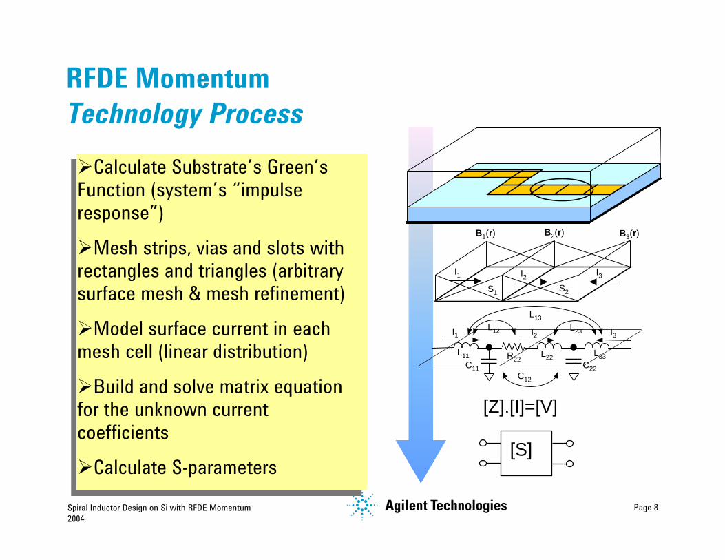
RFDE MomentumTechnology Process
B1(r) B2(r) B3(r)
I1 I2 I3S1 S2
[Z].[I]=[V]
I1 I2 I3
C11 C22C12
L11
L23
L22
L13L12
L33R22
[S]
Calculate Substrate’s Green’sFunction (system’s “impulseresponse”)Mesh strips, vias and slots withrectangles and triangles (arbitrarysurface mesh & mesh refinement)Model surface current in eachmesh cell (linear distribution)Build and solve matrix equationfor the unknown currentcoefficientsCalculate S-parameters
Calculate Substrate’s Green’sFunction (system’s “impulseresponse”)Mesh strips, vias and slots withrectangles and triangles (arbitrarysurface mesh & mesh refinement)Model surface current in eachmesh cell (linear distribution)Build and solve matrix equationfor the unknown currentcoefficientsCalculate S-parameters

Spiral Inductor Design on Si with RFDE Momentum2004
Page 9
Comparison of Models
• quasi-static inductance . . . . . . • quasi-static capacitance . . . . . • DC conductor loss (σ) . . . . . . . .• DC substrate loss (σ) . . . . . . . . • dielectric loss (tgδ) . . . . . . . . . . . . . . . . . . . . . . . . . . .• skin effect loss . . . . . . . . . . . . . . . . . . . . . . . . . . . . . . . .• substrate wave radiation . . . . . . . . . . . . . . . . . . . . . . . . . . . . . . . . . . . . . . . . . . .• space wave radiation . . . . . . . . . . . . . . . . . . . . . . . . . . . . . . . . . . . . . . . . . . . . . .
Spiral Inductors
S-parameters
RF
Spice model S-parameters
MW
DC Spice Momentum RF Momentum MW

Spiral Inductor Design on Si with RFDE Momentum2004
Page 10
Momentum Microwave & RF – ApplicationsAPPLICATIONS
RFIC (Silicon) RF Module (MCM, LTCC) Microwave - hybrid (Alumina) Microwave - MMIC (GaAs)
Initial design/optimization
Final design/optimization
High-Speed Digital (SI, BGA)RF Board (FR4, Duroid)RF Package (Plastic)
Planar Antennas
Momentum RF Momentum MW
frequency
physicalsize
200 GHzDC

Spiral Inductor Design on Si with RFDE Momentum2004
Page 11
Overview
Spiral Inductor Models Availability & LimitationsMomentum Technology OverviewKey Physical Effects Considered in MomentumRFDE Momentum Solution ProcessMomentum Application BenchmarkSummary

Spiral Inductor Design on Si with RFDE Momentum2004
Page 12
Substrate Coupling & Radiation
Resistive loss of metallizationResistivity of Si substrateCapacitive coupling effects to Si substrate
Silicon h = 500 µmεr = 11.9 σ = 7.41 S/m
W = 15 um
SiO2 h = 5 µm εr = 4
Copper, t = 4 µm
SiO2 h = 3 µm εr = 4
Passivationh = 4 µm εr = 3.6
Copper, t = 0.66 µm
σ=4.5107S/m
Ground

Spiral Inductor Design on Si with RFDE Momentum2004
Page 13
Current Return Path & Frequency Dependency
Impedance = R + jωLImpedance = R + jωL
frequencyDC 100 MHz 350 MHz 1.4 GHz
Current follows the path of “least resistance”impedance

Spiral Inductor Design on Si with RFDE Momentum2004
Page 14
Current Distribution & Skin Effects
Current distribution in cross section of thick conductor as function of frequency
Example: RFIC process copper, w=15µm, t=4µm
w
t
t < δsw < 2δs
t < δsw > 2δs
2δs > t > δsw > 2δs
edge effectsingle-sidedskin effect
frequencyDC
High
Low
Current Density100 MHz 350 MHz
w = 2δs t = δs
σ=4.5e7 S/m1 MHz 75 µm10MHz 23.7 µm100MHz 7.5 µm1 GHz 2.37 µm
Skin depth of copper
ωµσδ 2=s
t > 2δsw > 2δs
double-sidedskin effect
1.4 GHz
t = 2δs
OR
isolated conductorconductor withground planeuniform current
distribution

Spiral Inductor Design on Si with RFDE Momentum2004
Page 15
t = 2 um t = 4 um t = 8 um
t=2um
t=4um
t=8um
sheet conductorthick conductor
thick conductor
Influence of the thickness on the external inductance of the trace-Using edge mesh to include edge effect-Using Ohms/square resistance (no skin effect)-Using thick conductor model
port 1 port 2
length = 100 µm
L(ω)R(ω)
Silicon h = 500 µmεr = 11.9 σ = 6.67 S/m
W = 15 um
SiO2 h = 5 µm εr = 4
Copper, t = 2, 4, 8 µm
SiO2 h = 3 µm εr = 4
Passivationh = 4 µm εr = 3.6
Copper, t = 0.66 µm
σ=4.5107S/m
Increased thickness: -lower resistance -lower external inductance
Thick Conductors Effects

Spiral Inductor Design on Si with RFDE Momentum2004
Page 16
Thick Conductor Modeling IssuesEdge Effect & Skin EffectHow does Momentum address Edge Effect and Skin Effect?•The edge mesh concept takes the edge effect into account
•The surface impedance concept takes the skin effect into account
How does the inclusion of the edge effect and the skin effect influencethe resistance and inductance of a trace?
port 1 port 2
length
L(ω)R(ω)
⋅σ=
)wt(lengthRDCNote:
Silicon h = 500 µmεr = 11.9 σ = 7.41 S/m
W = 15 um
SiO2 h = 5 µm εr = 4
Copper, t = 4 µm
SiO2 h = 3 µm εr = 4
Passivationh = 4 µm εr = 3.6
Copper, t = 0.66 µm
σ=4.5107S/m
Spiral Inductor Design on Si with RFDE Momentum2004
Page 17
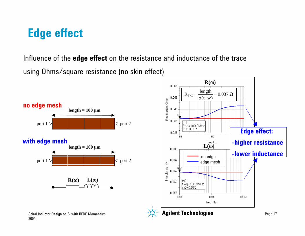
Influence of the edge effect on the resistance and inductance of the traceusing Ohms/square resistance (no skin effect)
no edge edge mesh
Ω=⋅σ
= 037.0)wt(
lengthR DC
Edge effect: -higher resistance -lower inductance
Edge effect
R(ω)
L(ω)
port 1 port 2
length = 100 µm
L(ω)R(ω)
port 1 port 2
length = 100 µmno edge mesh
with edge mesh

Spiral Inductor Design on Si with RFDE Momentum2004
Page 18
Silicon h = 500 µmεr = 11.9 σ = 7.41 S/m
W = 15 um
SiO2 h = 5 µm εr = 4
Copper, t = 4 µmSiO2 h = 3 µm εr = 4
Passivationh = 4 µm εr = 3.6
Copper, t = 0.66 µm
Influence of the skin effect on the resistance and inductance of a trace- using edge mesh to include edge effect- using surface current (sheet) model- using thick conductor expansion
port 1 port 2
length = 100 µm
L(ω)+ ∆L(ω)R(ω)
Skin effect: -higher HF resistance -higher internal inductance -lower external inductance
Skin effect: -higher HF resistance -higher internal inductance -lower external inductance
sheet model 1sheet model 2sheet model 3thick model
LHF
∆LDC
LDC∆LHF
RDC
RHF
single-sided skin effect
double-sided skin effect
single-sided skin effect
double-sided skin effect
no skin effect
t = δs t = 2δs
no skin effect
Skin Effects

Spiral Inductor Design on Si with RFDE Momentum2004
Page 19
Skin Effect – Discretization Problems
01
N
T
L
WH
Thick conductor is subdivided into Nlayers of thickness T/N and conductivity σ
Volume current is modeled with piecewiseconstant current filaments
How does a 3D volume meshing technology handles thick conductors?
N = 2N = 4N = 8N = 16N = 32N = 64
Need at least 3 subdivisionper skin depth forconvergence !!!
σ=4.5e7 S/m1 MHz 75 µm10MHz 23.7 µm100MHz 7.5 µm1 GHz 2.37 µm
Skin depth of copper
ωµσδ 2=s
Spiral Inductor Design on Si with RFDE Momentum2004
Page 20
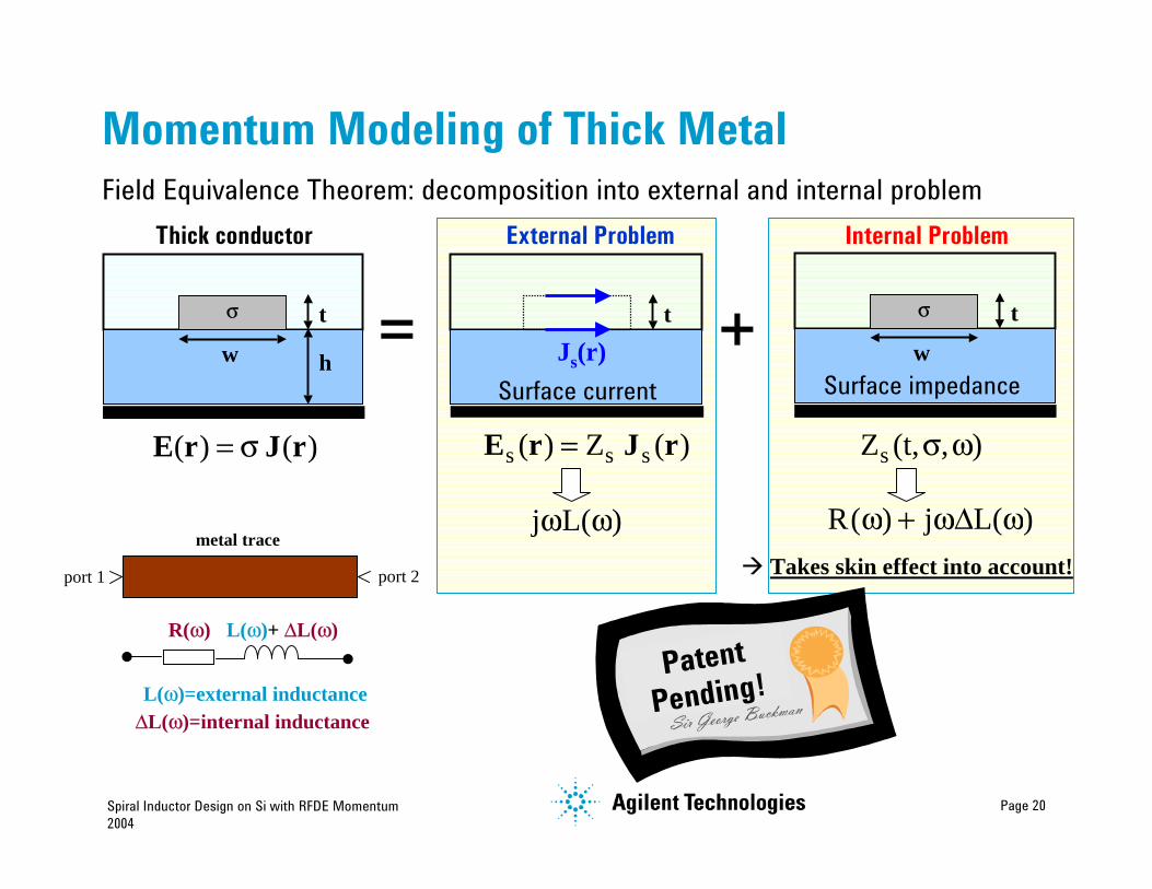
Momentum Modeling of Thick MetalField Equivalence Theorem: decomposition into external and internal problem
port 1 port 2
metal trace
L(ω)+ ∆L(ω)R(ω)
Thick conductor
w
t
h
σ
)( )( rJrE σ=
=
)( Z)( sss rJrE =
External Problem
t +Js(r)
Internal Problem
),(t,Zs ωσ
)L(j)(R ω∆ω+ω)L(j ωω
Surface current
L(ω)=external inductance∆L(ω)=internal inductance
Takes skin effect into account!
w
tσ
Surface impedance
PatentPending!

Spiral Inductor Design on Si with RFDE Momentum2004
Page 21
Thick Conductor Modeling
• Volume of thick conductor is divided into two equal sheet conductor layers, one atthe top surface and one at the bottom surface, with same conductivity and half of thethickness
• Additional via layer (perfect conducting) to short out differential mode• Actual distribution of top and bottom layer currents not enforced, but follows from
solution of EM equations, yielding improved model for resistance and inductance• Accuracy decreasing (horizontal currents on via layers missing) when w/t decreases
(w/t < 2) (this will be addressed in a future release)
)( ),,(Z)(
)( ),,(Z)(
2,s2t
s2,s
1,s2t
s1,s
rJrE
rJrE
ωσ=
ωσ=
External Problem
t +Js,1(r) wtσ
Internal Problem
),(t,Zs ωσSurface impedanceSurface current
Js,2(r)2-layers surface current
[1]
[2][3] σ, t/2
σ, t/2h2=t
h1
h3
3 substrate layers 2 strip layers + 1 via layer

Spiral Inductor Design on Si with RFDE Momentum2004
Page 22
Overview
Spiral Inductor Models Availability & LimitationsMomentum Technology OverviewKey Physical Effects Considered in MomentumRFDE Momentum Solution ProcessMomentum Application BenchmarkSummary
Spiral Inductor Design on Si with RFDE Momentum2004
Page 23
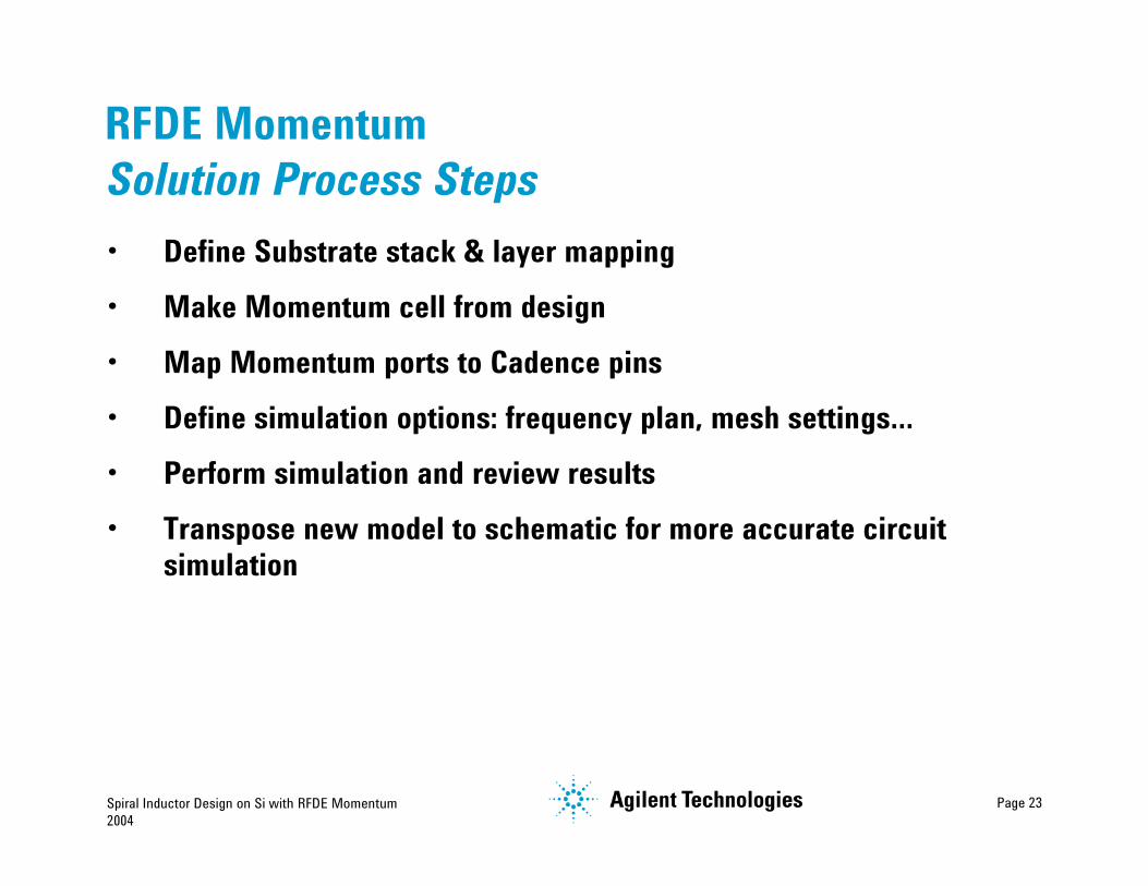
RFDE MomentumSolution Process Steps• Define Substrate stack & layer mapping• Make Momentum cell from design• Map Momentum ports to Cadence pins• Define simulation options: frequency plan, mesh settings…• Perform simulation and review results• Transpose new model to schematic for more accurate circuit
simulation
Spiral Inductor Design on Si with RFDE Momentum2004
Page 24
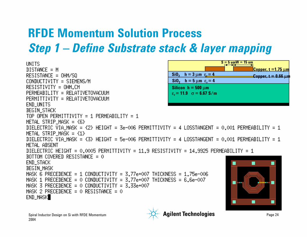
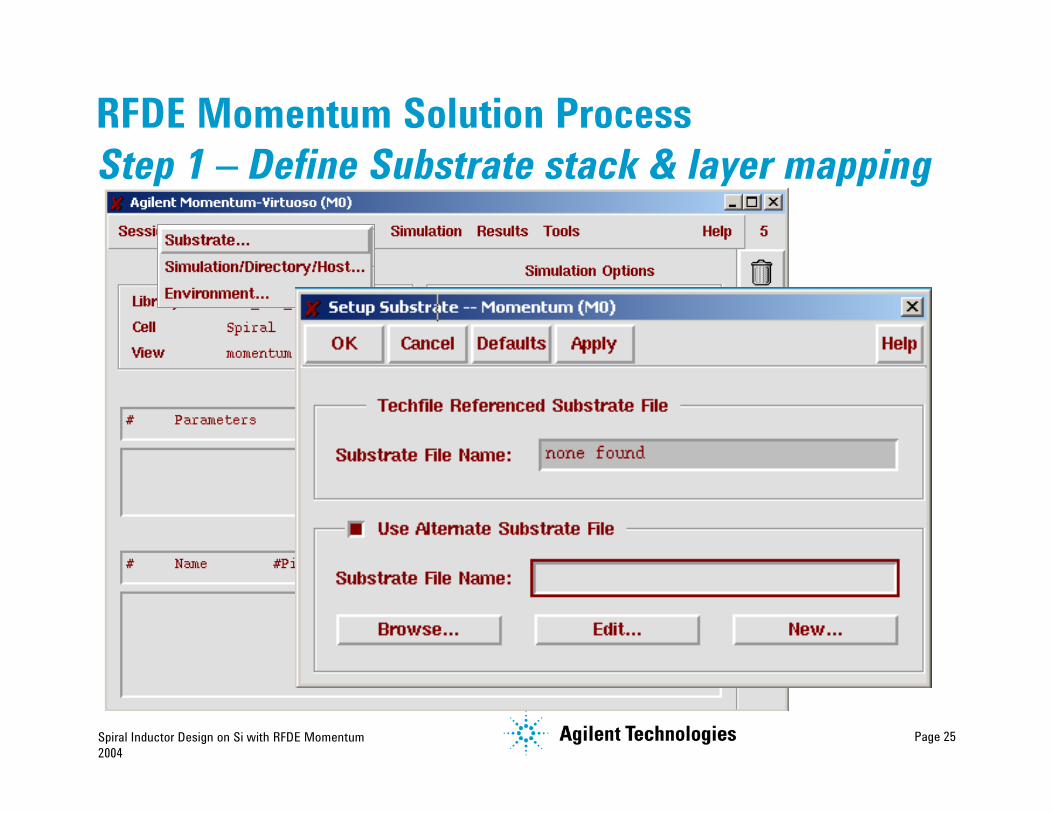
RFDE Momentum Solution ProcessStep 1 – Define Substrate stack & layer mapping
Silicon h = 500 µmεr = 11.9 σ = 6.67 S/m
W = 15 um
SiO2 h = 5 µm εr = 4
S = 5 um
Copper, t =1.75 µmSiO2 h = 3 µm εr = 4 Copper, t = 0.66 µm
Spiral Inductor Design on Si with RFDE Momentum2004
Page 25
RFDE Momentum Solution ProcessStep 1 – Define Substrate stack & layer mapping

Spiral Inductor Design on Si with RFDE Momentum2004
Page 26
RFDE Momentum Solution ProcessStep 1 – Define Substrate stack & layer mapping

Spiral Inductor Design on Si with RFDE Momentum2004
Page 27
RFDE Momentum Solution ProcessStep 2 – Make Momentum Cell

Spiral Inductor Design on Si with RFDE Momentum2004
Page 28
Momentum PortsMomentum Ports Cadence PinsCadence Pins
RFDE Momentum Solution ProcessStep 3 – Assign Ports to Cadence Pins

Spiral Inductor Design on Si with RFDE Momentum2004
Page 29
+ref -ref
port
RFDE Momentum Design FlowStep 3 – Assign Ports to Cadence Pins
Physical portsPhysical ports
Unphysical portsUnphysical portselectrically long distance
electrically short distance
electrically short distance

Spiral Inductor Design on Si with RFDE Momentum2004
Page 30
Frequency planMesh settingsMetallization properties…
RFDE Momentum Solution ProcessStep 4 – Define Simulation Options

Spiral Inductor Design on Si with RFDE Momentum2004
Page 31
RFDE Momentum Solution ProcessStep 5 – Perform EM Simulation & Review Results

Spiral Inductor Design on Si with RFDE Momentum2004
Page 32
RFDE Momentum Solution ProcessStep 5 – Perform EM Simulation & Review Results

Spiral Inductor Design on Si with RFDE Momentum2004
Page 33
RFDE Momentum Solution ProcessStep 5 – Perform EM Simulation & Review Results
Spiral Inductor Design on Si with RFDE Momentum2004
Page 34
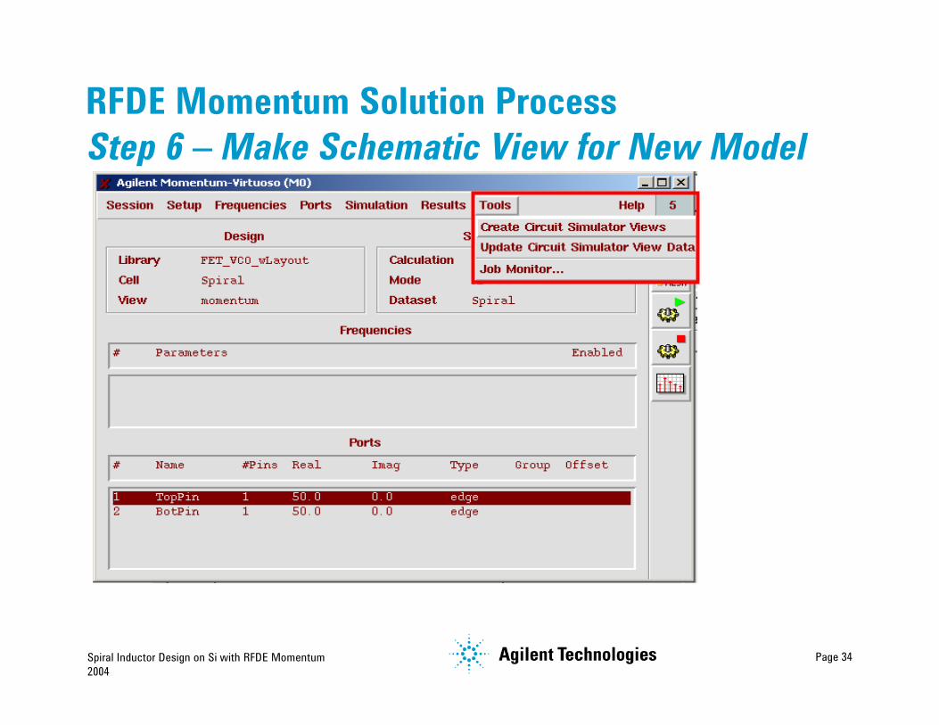
RFDE Momentum Solution ProcessStep 6 – Make Schematic View for New Model

Spiral Inductor Design on Si with RFDE Momentum2004
Page 35
RFDE Momentum Solution ProcessStep 6 – Transpose New EM Model to Schematic
Schematic Actions:1. Insert Momentum
components in Composer2. Set/Alter simulation control:
identical to case where noMomentum components areused
3. Run circuit simulation4. View/Analyze results
MomentumComponent
Momentum from Composer
Momentum from Composer
Can be used with Agilentcircuit simulator and CadenceSpectre (v5.0.33)
Can be used with Agilentcircuit simulator and CadenceSpectre (v5.0.33)

Spiral Inductor Design on Si with RFDE Momentum2004
Page 36
Overview
Spiral Inductor Models Availability & LimitationsMomentum Technology OverviewKey Physical Effects Considered in MomentumRFDE Momentum Solution ProcessMomentum Application BenchmarkSummary

Spiral Inductor Design on Si with RFDE Momentum2004
Page 37
Momentum – Application Benchmark“Momentum validated against results forstandard parts… This leads to a substantialimprovement in phase noise of a 4GHz testoscillator” Dr. M P Wilson
Source: “Modeling of integrated VCOresonators using Momentum” Dr. M PWilson, Tality UK.
Source: “Modeling of integrated VCOresonators using Momentum” Dr. M PWilson, Tality UK.

Spiral Inductor Design on Si with RFDE Momentum2004
Page 38
Momentum – Application Benchmark
2.5 Turn Octagonal Spiral Inductor
“Three test inductors were compared with measuredresults. All three inductor examples show good agreementwith measured results, showing that we could producereliable Momentum models for the particular processused.” Dr. M P Wilson.
“Three test inductors were compared with measuredresults. All three inductor examples show good agreementwith measured results, showing that we could producereliable Momentum models for the particular processused.” Dr. M P Wilson.

Spiral Inductor Design on Si with RFDE Momentum2004
Page 39
Momentum – Application Benchmark
“It can be seen that the Balun circuit improves phasenoise by means of an increase in the effective Q of theresonator. This clearly shows the benefit of the custommodeling facility given by Momentum.”Dr. M P Wilson
“It can be seen that the Balun circuit improves phasenoise by means of an increase in the effective Q of theresonator. This clearly shows the benefit of the custommodeling facility given by Momentum.”Dr. M P Wilson

Spiral Inductor Design on Si with RFDE Momentum2004
Page 40
Overview
Spiral Inductor Models Availability & LimitationsMomentum Technology OverviewKey Physical Effects Considered in MomentumRFDE Momentum Solution ProcessMomentum Application BenchmarkSummary

Spiral Inductor Design on Si with RFDE Momentum2004
Page 41
Summary
• Spiral inductors are critical RFIC design components• Foundries’ supplied models may limit design options• Electromagnetic-based modeling approach has many advantages• Method-of-Moments EM technique is best suited for modeling spirals• Momentum industry track record• RFDE Momentum solution process is a simple few steps process• RFDE Momentum is fully integrated with Cadence Virtuoso• RFDE Momentum added accuracy greatly enhances first-pass design
success

Spiral Inductor Design on Si with RFDE Momentum2004
Page 42
Appendix
• Momentum Substrate Stack Definition• Modeling Metal Losses

Spiral Inductor Design on Si with RFDE Momentum2004
Page 43
Momentum Substrate Definition
Momentum uses a text file for the description of the substratedefinition, which includes:
• Layers stack definition• Dielectric layers physical properties• Metal layers physical properties

Spiral Inductor Design on Si with RFDE Momentum2004
Page 44
1. Layers Stack Definition

Spiral Inductor Design on Si with RFDE Momentum2004
Page 45
2. Dielectric Layers’ Physical Properties
Spiral Inductor Design on Si with RFDE Momentum2004
Page 46
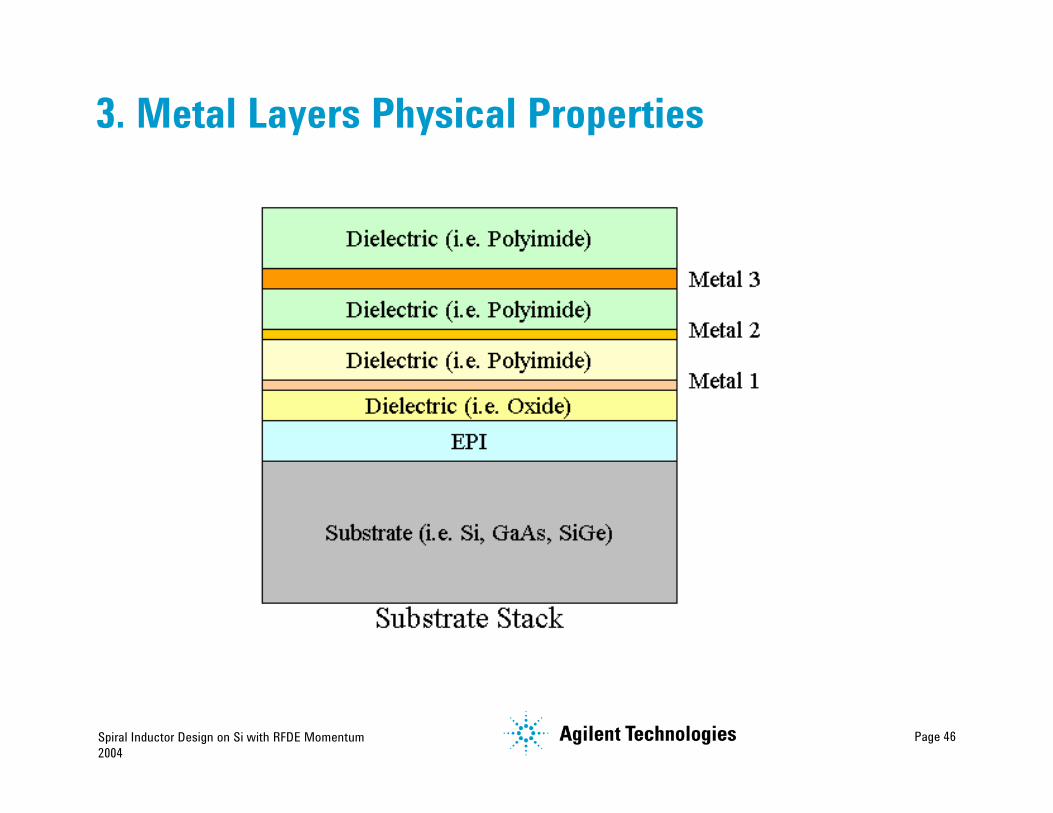
3. Metal Layers Physical Properties
Spiral Inductor Design on Si with RFDE Momentum2004
Page 47
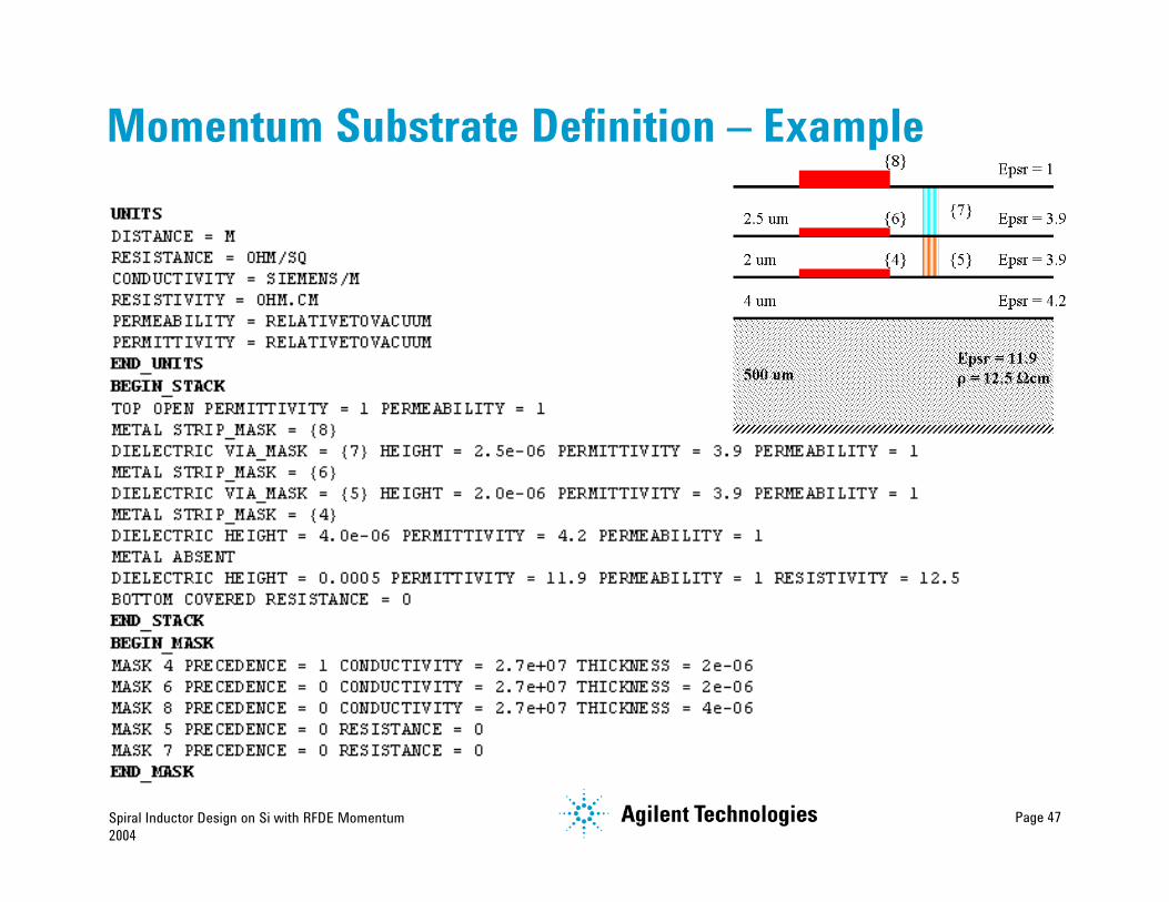
Momentum Substrate Definition – Example

Spiral Inductor Design on Si with RFDE Momentum2004
Page 48
Modeling Metal LossesDefault Model: Sheet Conductor Model
)( Z)( sss rJrE =
external problem
t +Js(r) w
tσ
internal problem
),(t,Zs ωσSurface impedanceSurface current
• Surface impedance based on 1-dimensional field approximation (only variation in z-direction), valid for good conductors (σ > ωε) with a high width/thickness ratio(typically w/t > 5)
• Models a uniform current distribution over entire cross section at low frequencies,yielding the correct DC resistance value
• Models a concentrated current distribution over skin depth δs at high frequencies, overestimates HF resistance (depending on closeness of return current in ground plane)
• Models the external inductance for zero thickness with higher internal inductance (skineffect), hence over estimates inductance

Spiral Inductor Design on Si with RFDE Momentum2004
Page 49
Modeling Metal LossesSurface Currents – Sheet Conductors
• Volume of thick conductor is modeled as an infinitely thin conductor layer• Surface current flows in one sheet conductor layer• External inductance L(ω) is independent of conductor thickness (t)
σt
thick conductor
J(r)
1-layer surface current
Js(r)un
strip (σ, t)
)( Z)( sss rJrE =
)L(j ωω

Spiral Inductor Design on Si with RFDE Momentum2004
Page 50
Modeling Metal LossesSurface Currents – Thick Conductors
•Volume of thick conductor is divided into two equal conductor layers, one at thetop surface and one at the bottom surface, with same conductivity and half of theconductor thickness
•Additional via layer (perfect conducting) included to short out differential mode•Actual distribution of top and bottom layer currents not enforced, but follows fromsolution of EM equations
•External inductance L(ω) is dependent on conductor thickness•As conductor thickness (t) increases: mutual inductance decreases externalinductance decreases; also, high frequency resistance decreases
σt
thick conductor
J(r)
2-layers surface current
un
via (perfect conducting)strip (σ, t/2)
strip (σ, t/2)Js,2(r)
Js,1(r)
t

Spiral Inductor Design on Si with RFDE Momentum2004
Page 51
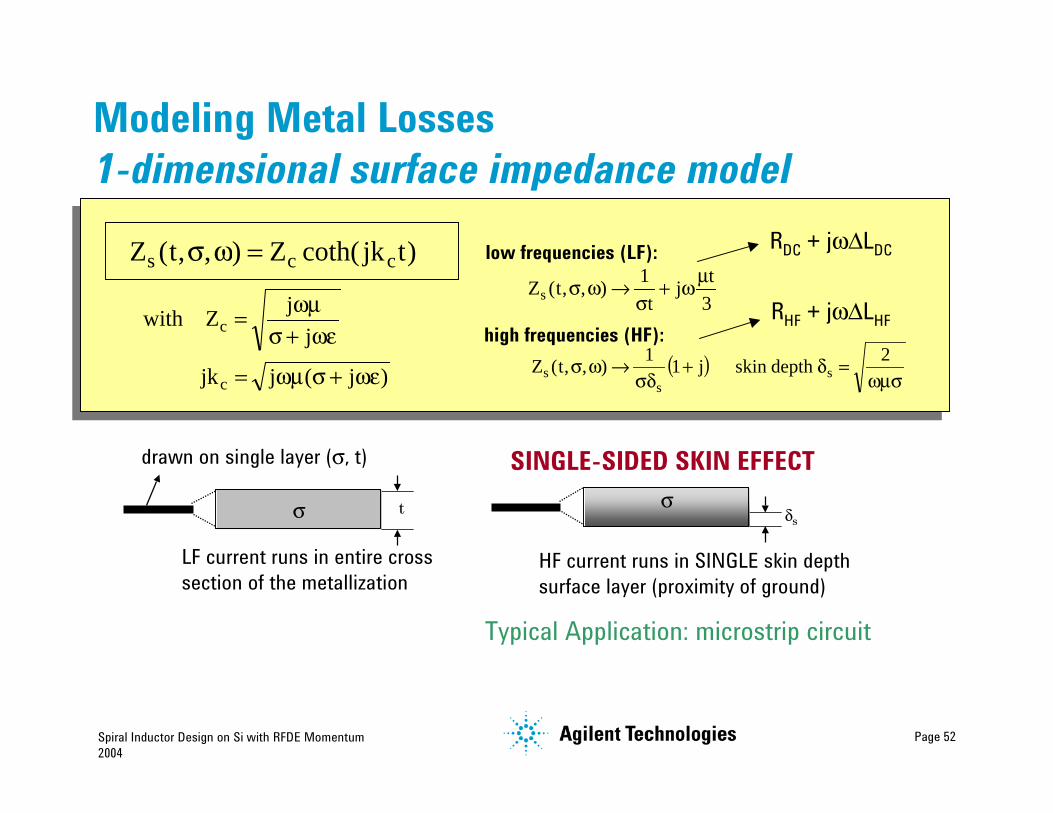
Modeling Metal Losses1-dimensional surface impedance model
• Distribution of the current inside the conductor is based on 1-dimensional fieldapproximation (only variation in z-direction), valid for good conductors (σ > ωε)with a high width/thickness ratio (typically w/t > 5)
• Yields analytic model for the surface impedance Zs(t,σ,ω)• Resistance R(ω) and interior inductance ∆L(ω) are dependent on: conductor
thickness, conductivity, and frequency (skin effect)
σt
thick conductor
J(r) )tjkcoth(Z),,t(Z ccs =ωσ
)j(jjk
jj Zwith
c
c
ωε+σωµ=
ωε+σωµ=
)( Z)( sss rJrE =
Spiral Inductor Design on Si with RFDE Momentum2004
Page 52
)tjkcoth(Z),,t(Z ccs =ωσ
3tj
t1),,t(Zs
µω+σ
→ωσ
low frequencies (LF):
high frequencies (HF):( )
ωµσ=δ+
σδ→ωσ 2depth skin j11),,t(Z s
ss
LF current runs in entire crosssection of the metallization
drawn on single layer (σ, t)
HF current runs in SINGLE skin depthsurface layer (proximity of ground)
δsσσ t
)j(jjk
jj Zwith
c
c
ωε+σωµ=
ωε+σωµ=
RDC + jω∆LDC
RHF + jω∆LHF
Modeling Metal Losses1-dimensional surface impedance model
SINGLE-SIDED SKIN EFFECT
Typical Application: microstrip circuit

www.agilent.com/fi nd/emailupdatesGet the latest information on the products and applications you select.
www.agilent.com/fi nd/agilentdirectQuickly choose and use your test equipment solutions with confi dence.
Agilent Email Updates
Agilent Direct
www.agilent.comFor more information on Agilent Technologies’ products, applications or services, please contact your local Agilent office. The complete list is available at:www.agilent.com/fi nd/contactus
AmericasCanada (877) 894-4414 Latin America 305 269 7500United States (800) 829-4444
Asia Pacifi cAustralia 1 800 629 485China 800 810 0189Hong Kong 800 938 693India 1 800 112 929Japan 0120 (421) 345Korea 080 769 0800Malaysia 1 800 888 848Singapore 1 800 375 8100Taiwan 0800 047 866Thailand 1 800 226 008
Europe & Middle EastAustria 0820 87 44 11Belgium 32 (0) 2 404 93 40 Denmark 45 70 13 15 15Finland 358 (0) 10 855 2100France 0825 010 700* *0.125 €/minuteGermany 01805 24 6333** **0.14 €/minuteIreland 1890 924 204Israel 972-3-9288-504/544Italy 39 02 92 60 8484Netherlands 31 (0) 20 547 2111Spain 34 (91) 631 3300Sweden 0200-88 22 55Switzerland 0800 80 53 53United Kingdom 44 (0) 118 9276201Other European Countries: www.agilent.com/fi nd/contactusRevised: March 27, 2008
Product specifi cations and descriptions in this document subject to change without notice.
© Agilent Technologies, Inc. 2008
For more information about Agilent EEsof EDA, visit:
www.agilent.com/fi nd/eesof