Embed Size (px)
Citation preview

Progress In Electromagnetics Research C, Vol. 79, 159–173, 2017
Design of RF Sensor for Simultaneous Detection of ComplexPermeability and Permittivity of Unknown Sample
Pratik Porwal1, *, Azeemuddin Syed1,Prabhakar Bhimalapuram2, and Tapan Kumar Sau2
Abstract—In this paper, a novel microwave planar resonant sensor is designed and developed forsimultaneous detection of permittivity and permeability of an unknown sample using a nondestructivetechnique. It takes advantage of two-pole filter topology where the interdigitated capacitor (IDC) andspiral inductor are used for placement of a sample with significant relative permittivity and permeabilityvalues. The developed sensor model has the potential for differentiating permittivity and permeabilitybased on the odd mode and even mode resonant frequencies. It operates in the ISM (industrial,scientific and medical) frequency band of 2.2–2.8 GHz. The sensor is designed using the full waveelectromagnetic solver, HFSS 13.0, and an empirical model is developed for the accurate calculationof complex permittivity and permeability of an unknown sample in terms of shifts in the resonantfrequencies and transmission coefficients (S21) under loaded condition. The designed resonant sensorof size 44×24 mm2 is fabricated on a 1.6 mm FR4 substrate and tested, and corresponding numericalmodel is experimentally verified for various samples (e.g., magnetite, soft cobalt steel (SAE 1018), ferritecore, rubber, plastic and wood). Experimentally, it is found that complex permeability and permittivitymeasurement is possible with an average error of 2%.
1. INTRODUCTION
The field of sensing and characterization of an unknown sample is an imperative area of biology, solidstate physics, material science and electronics engineering. The traditional chemical methods used forsensing are cumbersome (several reaction steps), time consuming, destructive and requires large volumeof testing sample [1–3]. As a result in recent years, cell scale analysis using electrochemical, optical,piezoelectric, thermal, or mechanical principles which falls under electronics, optics, and informaticscategories becomes influential tools in the clinical diagnostic field [4]. All these tools allow rapid,sensitive, real time measurements, and these techniques are label-free [5]. Therefore, the nondestructivesensing using RF and microwave frequency is an effective technique.
There are different RF sensing techniques available, which are categorized under the nonresonantand resonant methods [6]. The nonresonant methods are normally used for wide-band characterizationof samples with moderate accurate results [7]. Therefore, the resonant methods are preferred overnonresonant methods for obtaining accurate results over a narrow band of operation. Among theresonant methods, the sensing and characterization of a sample can be performed either usingrectangular waveguide cavity resonator [8], H-slot cavity resonator [9] or with the help of planar resonantsensors [10]. Since cavity resonator technique requires bulky and costly metallic cavity, the planarresonant sensors are preferred because of advantages such as low cost, easy fabrication and integrationwith other microwave circuits [11]. Designs of the planar resonant sensor are mostly based on various
Received 4 September 2017, Accepted 31 October 2017, Scheduled 13 November 2017* Corresponding author: Pratik Porwal ([email protected]).1 Center of VLSI and Embedded System Technology (CVEST), IIIT, Hyderabad-500032, India. 2 Center for Computational NaturalSciences and Bioinformatics (CCNSB), IIIT, Hyderabad-500032, India.

160 Porwal et al.
resonant structures such as split ring resonators (SRR) [12–15], complementary split ring resonators(CSRR) [16], substrate integrated waveguide (SIW) [17, 18], slotline based RF sensor [19], steppedimpedance resonator (SIR) [20], series resonators [21], fractal capacitors [22], spiral inductors [23] andinterdigitated capacitor (IDC) [24]. Among these different resonant structures, the fractal capacitors,spiral inductors, IDC are easy to get fabricated on microstrip line and provide a reasonably high amountof sensitivity. On the contrary, in the case of the SRR and CSRR structures, the resonant structure iscoupled to the microstrip line either electrically or magnetically depending upon the orientation of theresonator with the microstrip line [25], thus reducing their sensitivity.
RF resonant sensors find variety of applications in estimating the permittivity of different polarand non-polar organic chemical solvents, detection of adulteration in oils and permeability of magneticparticles present in a sample, haemoglobin in blood [26], etc. However, two different resonantsensors [27, 28] are required to sense permittivity and permeability independently. This makes thesystem complicated and increases its cost and size.
In this paper, a planar resonant RF sensor based on a combination of spiral inductor and IDCstructure is proposed for simultaneous detection of permittivity and permeability of an unknown sample.The proposed structure is etched on the main microstrip line for getting the maximum sensitivity, andthe basic design is carried out using the HFSS 13.0. The design specifications of each individual structureand corresponding frequency response of both even and odd quasi Tranverse Electromagnetic (TEM)mode are derived for the proposed design. The numerical data obtained from the finite integrationtechnique based approach are used to develop an empirical model of the proposed sensor. The developednumerical model is used to calculate the real part and tangent loss of the permittivity and permeabilityof a sample on the basis of shift in odd and even mode resonant frequencies and transmission coefficients.This proposed sensor of size 44 mm × 24 mm is fabricated on a 1.6 mm thick FR-4 substrate operatingin the frequency range of 2.2–2.8 GHz. The resonant frequency and magnitude of the transmissioncoefficient of the magnetic and dielectric samples are measured using the vector network analyzer (VNA)and analysed in detail. The measurement of various standard samples (i.e., magnetite, soft cobalt steel,ferrite core, rubber, plastic and wood) using proposed sensor ensures that the error in calculation ofcomplex permittivity and permeability is around 2%.
2. PROPOSED DESIGN OF RF RESONANT SENSOR
The proposed RF resonant sensor is designed using two spiral inductors and IDC as shown in Fig. 1(a).The spiral inductors are connected in series with IDC, whereas both spiral inductors are also in seriesthrough underpass as shown in Fig. 1(b) and Fig. 1(c). For testing procedures, the unknown sample isplaced at the spacing between two inductors and IDC fingers such that it covers the most sensitive areaof the sensor. The basic series RLC circuit model of the proposed sensor is as shown in Fig. 1(d).
The series resonant branches of LIDC Cg model the two halves of the IDC, where Cg presents thecapacitive effect between the metallic halves through ground plane, and Lg models the inductive pathsof IDC structure. Here, Cm stands for the mutual capacitive effect between the IDC fingers. Spiralinductor is in series with IDC, and the corresponding inductance is denoted by LInd. These coupledinductors and capacitor interact with each other through electrical and magnetic couplings.
2.1. Design Specifications
Spiral inductor and IDC are the chief constituents of the proposed design, and each element is discussedas follows.
2.1.1. IDC Structure
The structure of IDC is shown in Fig. 2. The coplanar geometry can be transformed into a parallelplate geometry using conformal transformation technique [29]. The capacitance of IDC (CIDC) can nowbe calculated as
Cm = nx(C1 + C2) pF, (1)

Progress In Electromagnetics Research C, Vol. 79, 2017 161
(a) (b)
(c) (d)
Figure 1. (a) 3D view and (b) metal layer view of proposed biosensor design using two spiral inductorand Interdigitated capacitor (c) layout of the ground plane (d) electrical circuit model of proposedsensor.
x Length of finger 10 mma Width of finger 1 mmd Spacing between fingers 0.75 mmn No of fingers 6h Height of a substrate 1.6 mm
εsub Dielectric constant of a substrate 3.9ε′r Dielectric constant of a test sample —
(a) (b)
Figure 2. (a) Top view and (b) cross sectional view of IDC structure.
where x is the length of IDC finger, n the total number of fingers, and C1 and C2 are the line capacitanceof coplanar strip with air and dielectric substrate, respectively. C1 and C2 are given as [29]
C1 = 4ε0ε′r
K(k′1)
K(k1)pF/cm, (2)
C2 = 2ε0(εsub − 1)K(k′
2)K(k2)
pF/cm, (3)

162 Porwal et al.
k1 =(
1 +2a
2d + a
)⎛⎜⎝√√√√ 1
1 +2ad
⎞⎟⎠ , (4)
k′1 =
√1 − k2
1 , (5)
k′2 =
sinh(πa
4h
)sinh
( π
2h
(a
2+ d)) ×
√√√√√√√sinh2
(π
2h
(3a2
+ d
))− sinh2
( π
2h
(a
2+ d))
sinh2
(π
2h
(3a2
+ d
))− sinh2
(πa
4h
) , (6)
k2 =√
1 − k′22 , (7)
K(k)K(k′)
=2π
ln
(2
√1 + k
1 − k
). (8)
Here, K(k) is a complete elliptical integral of the first kind.
2.1.2. Inductor Design
Dout outer dimension of spiral 10 mmw Line Width 1 mms Spacing between lines 1 mmN No of turns 2
Figure 3. Design of two spiral inductor connected through underpass.
The structure of two spiral inductors is as shown in Fig. 3. Both spiral inductors are in series andconnected through underpass. For such a symmetrical structure, the total length (ltot) of the inductoris given by [30]
ltot = 4N (Dout − w − (N − 1)(w + s)) , (9)where, N is the number of turns, Dout the outer diameter of spiral, w the metal width, and s the spacingbetween segments. The total inductance of an inductor consists of the inductor self-inductance (Lself )and of the remaining part, which comes from the total negative (M− ) and total positive (M+) mutualinductances that include all negative and positive interactions among all segments of inductor. Theself-inductance of the square inductor can be expressed as [30]
Lself = 2 × 10⁻⁷ × ltot × ln(
ltot
w+ 1.193 + 0.2235
w
ltot
)H. (10)
The expressions for mutual inductances are simple and easy to understand resulting from the symmetryproperties of the square geometry. The total negative mutual inductance can be expressed as [31]
M− = 0.47 × μ
2π× N × ltot H. (11)
The third constitutive element of the total inductance is the total positive mutual inductance. Theaverage distance (d+) for the constituting factor of positive mutual inductance can be calculated by
d+ =(w + s)(N + 1)
3(12)

Progress In Electromagnetics Research C, Vol. 79, 2017 163
The total positive mutual inductance is [32]
M+ =μ
2π× ltot × (N − 1) ×
⎛⎝ln
(√1 + p2 + p
)−⎛⎝√
1 +(
1p
)2
+1p
⎞⎠⎞⎠ H, (13)
wherep =
ltot
4Nd+(14)
Thus, the total inductance (Ltot) of the spiral inductor is given as
Ltot = Lself + M+ − M− H. (15)
2.2. E-Field and H-Field Analysis
The sensor design takes advantage of two-pole filter topology, and IDC allows electromagnetic energytransfer from one port to the other. The electric field is strong and homogeneous between fingers ofthe IDC, whereas magnetic field is strong and homogeneous across the inductor as shown in Fig. 4.The electric field between fingers is 2.677 × 10³ V/m and near inductor is 4.321 × 10² V/m. Since veryweak electric field is experienced near the surface of the inductor as compared to IDC, the area betweenfingers is the most sensitive region for detection of permittivity. On the contrary, magnetic field acrossthe inductors is 2.93 A/m and is minimum at IDC area. Therefore, the gap between inner diameters oftwo inductors is the most sensitive region for detection of permeability of a sample.
(a) (b)
Figure 4. (a) Electric field distribution and (b) magnetic field distribution at the surface of proposedsensor.
2.3. Frequency Response of Proposed Sensor
Figure 2 illustrates the cross section of a pair of coupled microstrip lines (IDC strucure) underconsideration in this section, where these microstrip lines of width a are in the edge-coupled configurationwith a separation d. Therefore, this structure supports two quasi-TEM modes, i.e., the even modeand odd mode. Frequency response of the sensor is same as that of the dual-bandstop RF filter. Ithas two resonant frequencies, which are separated from each other as shown in Fig. 5. These tworesonant frequencies are due to propagation of odd mode and even mode [33]. These two TEM modesof wave propagation can be characterized by the even mode characteristic impedance Ze and odd modecharacteristic impedance Zo. Ze is defined as the characteristic impedance between one line and theground when equal and in phase voltages are impressed on the two lines, and Zo is defined as thecharacteristic impedance between one line and the ground when equal but opposite phase voltages areimpressed. The propagation constants and phase constant for these modes are given by [34]
γo,e = [(Y0 ± Ym)(Z0 ∓ Zm)]1/2 , (16)

164 Porwal et al.
2.2 2.3 2.4 2.5 2.6 2.7 2.8
Frequency(GHz)
-80
-70
-60
-50
-40
-30
-20
-10
0
S21
(dB
)
HFSS SimulationLumped circuit simulationMeasured
Figure 5. Simulated and measured frequency response of proposed sensor.
(a) (b) (c) (d)
Figure 6. (a) Electric and magnetic field distributions at even mode. (b) Electric and magnetic fielddistributions at odd mode. (c) Even-mode circuit model of IDC. (d) Odd-mode circuit model of IDC.
where, Y0 and Ym are the self and mutual admittances, and Z0 and Zm are the self and mutualimpedances. The propagation constant is a complex quantity, and it is given by [35],
γo,e = αo,e + jβo,e, (17)
where, αo,e is the attenuation constant and βo,e the phase constant
βo,e = ω (L0C0 − LmCm ± (LmC0 − L0Cm))1/2 rad/m. (18)
The impedances of odd mode and even mode are given by [36]
Ze =ω
βe(L0 − Lm)Ω, (19)
Zo =βo
ω
(1
C0 + Cm
)Ω. (20)
The impedance lines are characterized by inductance per unit length L0 and capacitance per unit lengthC0. Lm is the mutual inductance, Cm the mutual capacitance, and ω the operating frequency.
Electric and magnetic field distributions in design at odd mode and even mode are as shown inFigs. 6(a) and 6(b). The even mode only depends on the magnetic coupling, and the resonant frequency(fe) is more sensitive to the inductors, whereas the odd mode mainly relies on the electric coupling andits frequency (fo) changes as a function of the interdigitated capacitance value. It can be inferred from

Progress In Electromagnetics Research C, Vol. 79, 2017 165
Fig. 2 (equivalent circuit) that the particle can exhibit the even and odd-mode resonances with theequivalent circuits demonstrated in Figs. 6(c) and 6(d), respectively. In the even mode, the two halvesof the resonator have the same voltage distribution. Thus, and no current will pass through Cm, and itwill be open-circuited. Conversely, in the odd mode, there will be a virtual ground across the electricwall, and CM is broken into two equal parts of 2Cm. Based on Fig. 2, Fig. 7(c), Fig. 7(d) and the abovediscussion, the even- and odd-mode resonance frequencies can be defined as
fe =1
2π√
((LIDC + LInd))Cg
Hz, (21)
fo =1
2π√
((LIDC + LInd))(Cg + 2Cm)Hz. (22)
3. SIMULATION RESULTS AND NUMERICAL MODELING
In this section, we discuss frequency response of the designed sensor before and after addition of asample with different permeabilities and permittivities at different positions on sensors.
3.1. Addition of Sample with Significant Relative Permeability
After modeling the sensor, the magnetic samples (mangetite, SAE 1018, Ferrite core) havingpermeability between 1–20 are added in the sensor, and corresponding shifts in the resonant frequencyare observed for each permeability value as compared to the unloaded case of the sensor as shown inFig. 7. Moreover, the magnitude of even-mode frequency shift is directly proportional to the permeabilityvalue of the sample. Table 1 gives details of the frequency shifts for permeability values of test samples.After observation of different shifts in resonant frequency for variation in relative permeability, theempirical formula derived using Equations (1)–(15) and (21) for determining the real part of permeability
2.3 2.4 2.5 2.6 2.7 2.8
Frequency(GHz)
-70
-60
-50
-40
-30
-20
-10
0
S21
(dB
)
Unloaded SensorMagnetite ( µ '
r = 1.6)
SAE 1018 ( µ 'r = 4.976)
Ferrite (F22) ( µ 'r = 19)
2.5 2.55 2.6 2.65 2.7 2.75 2.8
Frequency(GHz)
-70
-60
-50
-40
-30
-20
-10
0
S21
(dB
)
Unloaded SensorMagnetite ( µ '
r = 1.6)
SAE 1018 ( µ 'r = 4.976)
Ferrite (F22) ( µ 'r = 19)
Figure 7. Frequency response of the sensor before and after addition of sample with differentpermeability value.
Table 1. Even mode resonant frequency shifts after addition of different permeability.
Test Relative Even mode resonantsample permeability frequency Shift
Magnetite 1.6 4.5 MHzSAE 1018 4.976 24 MHz
Ferrite core (F22) 19 45 MHz

166 Porwal et al.
is given by,
μ′r =
11.16
(30.7648
(2.969 − 0.040487 × Δf)2− 2.0685
)(23)
where, μ′r is the relative permeability of the unknown sample and Δf the frequency shift (MHz).
Similarly, the tangent loss is varied from 0.001 to 0.1, and the shifts in transmission coefficients areobserved as shown in Fig. 8. The empirical formula derived using Equations (1)–(15), (21) and processexplained in [37] to calculate tangent loss of a unknown material is given by,
tan δ =1
0.71764 μ′r
log
(S21 + 53.1244 + 0.137 × 100.153µ′
r
| − 8.3142 + 0.7364 μ′r|
)(24)
where, S21 is transmission coefficient (dB).
2.655 2.66 2.665 2.67 2.675
Frequency(GHz)
-55
-50
-45
-40
-35
-30
S21
(d
B)
tan = 0tan = 0.02tan = 0.04tan = 0.06tan = 0.08tan = 0.1
Figure 8. Variation of S21 (dB) magnitude of sensor with loss tangent value ranging from 0 to 0.1 forμr = 6.
Due to higher magnetic field, spacing between inner diameters of the inductor is an effective positionfor addition of a sample with significant permeability. Addition of a sample with permeability changesmagnetic coupling and causes a shift in even-mode resonant frequency only. Addition of a sample withsignificant relative permeability between IDC fingers results in no change in frequency response due toweak magnetic field.
3.2. Addition of Sample with Significant Relative Permittivity
The dielectric samples (rubber, plastic, white marble, magnetite and ferrite) are added, and thecorresponding resonant frequency shifts are observed for each relative permittivity value comparedto the unloaded case of the sensor as shown in Fig. 9. Moreover, the magnitude of odd-mode frequencyshift is proportional to the permittivity value of the sample. Table 2 gives details of the frequencyshift for various test samples. After observation of different frequency shifts in resonant frequencyfor variation in permittivity, the empirical formula derived by using Eqs. (1)–(15), (22) and processexplained in [37] for determining the real part of permittivity of an unknown sample is given by,
ε′r =1
0.7712
(10(1.5725−2 log(2.36006−0.02015×Δf)) − 4.984
)(25)
where, ε′r is the relative permittivity of the unknown sample and Δf the frequency shift (MHz).Tangent loss is varied from 0.001 to 0.1, and the corresponding shift in transmission coefficient is
observed as shown in Fig. 10. The empirical formula for determining the tangent loss of permittivity is
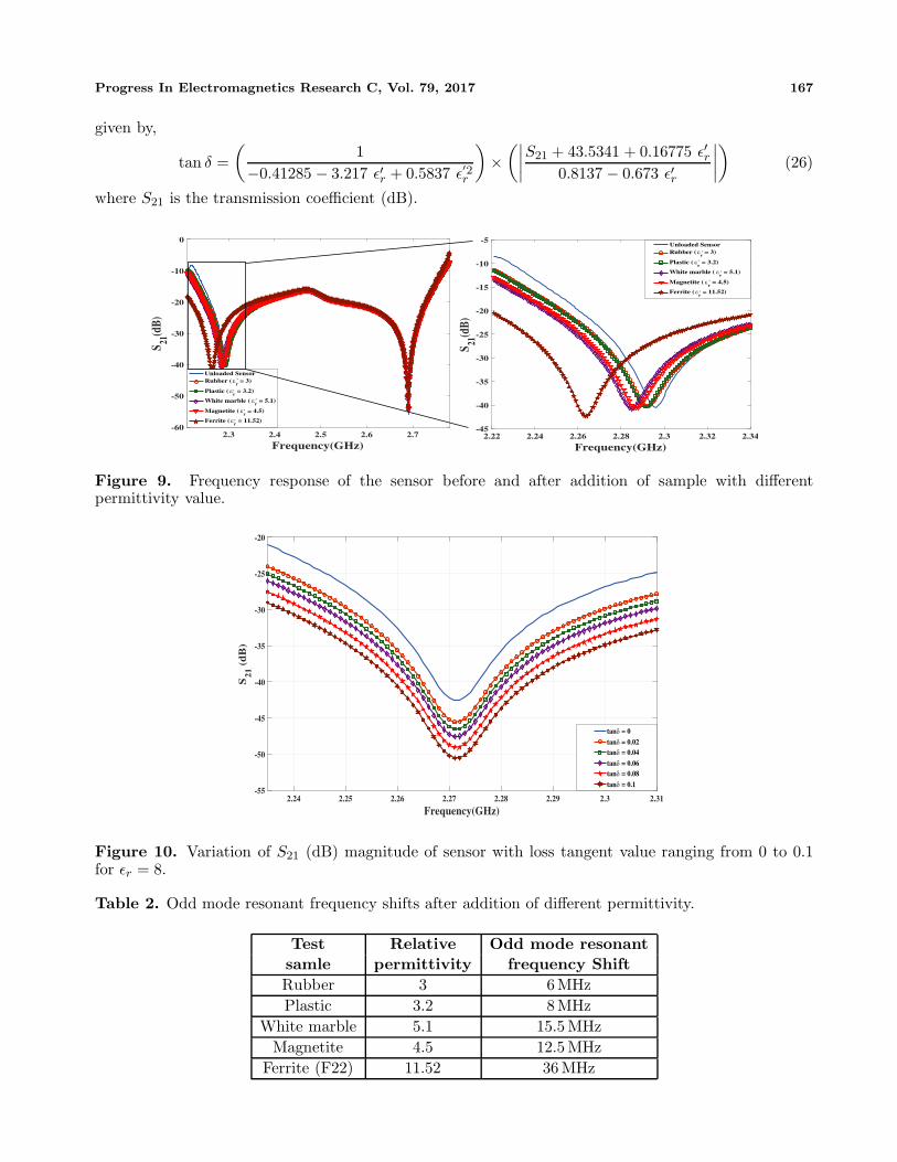
Progress In Electromagnetics Research C, Vol. 79, 2017 167
given by,
tan δ =(
1−0.41285 − 3.217 ε′r + 0.5837 ε′2r
)×(∣∣∣∣S21 + 43.5341 + 0.16775 ε′r
0.8137 − 0.673 ε′r
∣∣∣∣)
(26)
where S21 is the transmission coefficient (dB).
2.3 2.4 2.5 2.6 2.7
Frequency(GHz)
-60
-50
-40
-30
-20
-10
0
S 21(d
B)
Unloaded SensorRubber (ε
r = 3)
Plastic (ε r = 3.2)
White marble ( ε r = 5.1)
Magnetite (ε r = 4.5)
Ferrite (ε r = 11.52)
2.22 2.24 2.26 2.28 2.3 2.32 2.34
Frequency(GHz)
-45
-40
-35
-30
-25
-20
-15
-10
-5
S 21(d
B)
Unloaded SensorRubber (ε
r = 3)
Plastic (ε r = 3.2)
White marble ( ε r = 5.1)
Magnetite (ε r = 4.5)
Ferrite (ε r = 11.52)
'
'
'
'
'
'
'
'
'
'
'
Figure 9. Frequency response of the sensor before and after addition of sample with differentpermittivity value.
2.24 2.25 2.26 2.27 2.28 2.29 2.3 2.31
Frequency(GHz)
-55
-50
-45
-40
-35
-30
-25
-20
S21
(d
B)
tanδ = 0
tanδ = 0.02tanδ = 0.04
tanδ = 0.06tanδ = 0.08
tanδ = 0.1
Figure 10. Variation of S21 (dB) magnitude of sensor with loss tangent value ranging from 0 to 0.1for εr = 8.
Table 2. Odd mode resonant frequency shifts after addition of different permittivity.
Test Relative Odd mode resonantsamle permittivity frequency ShiftRubber 3 6MHzPlastic 3.2 8MHz
White marble 5.1 15.5 MHzMagnetite 4.5 12.5 MHz
Ferrite (F22) 11.52 36 MHz

168 Porwal et al.
The gap between IDC fingers is an effective position for addition of a sample with significantpermittivity due to higher electric field. Addition of a sample with significant permittivity changes IDCcapacitance and causes a shift in odd-mode resonant frequency only. Due to weak electric field, nosignificant change in the frequency response is observed after the addition of a sample with significantrelative permittivity between the inductor spacing.
4. MEASUREMENT AND RESULTS
The sensor is fabricated using a standard photolithography technique on a commercially available 1.6 mmFR-4 substrate with a conductive copper film coating of 35 µm. Geometric pattern from a photo-maskwith the help of light-sensitive chemical photoresist is developed on the substrate, and the exposurepattern is engraved into the desired conductive film pattern. A pair of 50 Ω SMA connectors is thenmounted on the fabricated sensor through the mechanical welding for the measurement of reflectionand transmission data. The fabricated sensor (front and back view) and measurement setup are shownin Figs. 11(a), 11(b) and 11(c), respectively. The fabricated planar sensor length is 44 mm, and itswidth is 24 mm. The sensor is connected with the vector network analyzer (VNA) through coaxial SMAconnectors. All the measurements are performed using the Agilent N2293A Network Analyzer. Theinput power taken is 0 dBm, and number of sweep points is taken as 10001.
(a) (b) (c)
Figure 11. (a) Top view of fabricated sensor. (b) Bottom view of fabricated sensor. (c) Experimentalsetup.
After experimental setup, various material samples are added in the spacing between inductorsand IDC fingers. Samples are placed in the specified area (gap between two inductors) to avoid directcontact with inductor metal layer. This placement position helps to find accurate results withoutany short connection. Shifts in the resonant frequency and S21 (dB) magnitude are measured usingVNA as shown in Figs. 12 and 13. The measured resonant frequency and the transmission coefficientfor each specimen are then fitted into the developed numerical model, and the corresponding relativepermeability, relative permittivity and loss tangents are calculated using Eqs. (23), (24), (25) and (26),respectively, and shown in Tables 3 and 4. The measured results are also compared with standard
Table 3. Measured complex permeability using proposed sensor.
Resonant
frequency
(GHz)
S21
(dB)
Reference
value
[38–41]
Measured data Percentage error
MUT ↓ μ′r tan δ μ′
r tan δ %μ′r % tan δ
Magnetite (Fe3O4) 2.692 −45.154 1.6 0.0268 1.6395 0.02753 2.468 2.72388
Soft cobalt steel
(SAE 1018)2.672 −48.3357 4.976 0.01039 4.924 0.01085 1.045 4.427
Ferrite core (F22) 2.651 −45.451 19 — 18.9999 0.0531 0.00052 —–
Progress In Electromagnetics Research C, Vol. 79, 2017 169
available data, and the error percentage is calculated. From Tables 3 and 4, the results of complexpermittivity and permeability measurement using the proposed sensor are analogous with the standardvalues available in the literature [38–43].
Measurements of the real part and tangent loss of permeability and permittivity are possible with
Table 4. Measured complex permittivity using proposed sensor.
Resonant
frequency
(GHz)
S21
(dB)
Reference
value
[38–43]
Measured data Percentage error
MUT ↓ ε′r tan δ ε′
r tan δ %ε′r % tan δ
Rubber 2.298 −43.64 3.00 0.1639 3.1 0.157 3.333 4.209
Plastic 2.296 −46.0537 3.2 0.445 3.233 0.456 1.045 2.4719
White marble 2.289 −39.44 5.1 —– 4.985 0.0095 2.342 ——
Magnetite 2.292 −44.03 4.5 —— 4.32 0.031675 4.00 ——
Ferrite (F22) 2.2685 −38.87 11.52 —– 11.411 0.0235 0.946 ——
2.5 2.55 2.6 2.65 2.7 2.75 2.8 2.85 2.9Frequency(GHz)
-55
-50
-45
-40
-35
-30
S21(d
B)
Unloaded sensorMagnetite(Fe
3O
4)
Soft cobalt steel(SAE 1018)Ferrite core (F22)
Figure 12. Measured Even mode frequencyresponse for various magnetic samples.
2.2 2.25 2.3 2.35 2.4Frequency(GHz)
-50
-45
-40
-35
-30
-25
-20
-15S 21
(dB
)Unloaded SensorRubberPlasticWhite marbleMagnetiteFerrite (F22)
Figure 13. Measured odd mode frequency responsefor various dielectric samples.
2.1 2.2 2.3 2.4 2.5 2.6 2.7 2.8 2.9
Frequency(GHz)
-55
-50
-45
-40
-35
-30
-25
-20
-15
-10
S21(d
B)
Unloaded sensor
Magnetite(Fe3O
4)
(a)
2.1 2.2 2.3 2.4 2.5 2.6 2.7 2.8 2.9Frequency(GHz)
-55
-50
-45
-40
-35
-30
-25
-20
-15
-10
S2
1(d
B)
Unloaded sensor
Ferrite core (F22)
(b)
Figure 14. Frequency response of sensor after placement of (a) magnetite (b) ferrite (F22) betweenIDC fingers and inductor at the same time.

170 Porwal et al.
typical error between the range of 2%–5%. The error is obtained due to slight mismatch betweensimulated and fabricated designs.
After testing of sensor, a ferrite sample is added at both positions simultaneously. (i.e., spacingbetween inductor and IDC fingers). As ferrite composite posses magnetic and dielectric properties,significant shifts in both even mode and odd mode resonant frequencies are observed. Due to differentpermeability and permittivity values of ferrite, shifts in the resonant frequencies are different. Similarly,magnetite also exhibits magnetic and dielectric properties, and the corresponding permeability,permittivity and corresponding losses are measured. From Figs. 14(a) and 14(b), it is ensured thatthe proposed sensor allows real time, simultaneous and label-free measurement of permeability andpermittivity of unknown sample.
5. TEST SAMPLE SIZE AND THICKNESS ANALYSIS
The consideration of the size and thickness of the test sample between sensitive part of the sensor is quiteimportant for accurate measurement of the complex permeability and permittivity. 32 mm2 and 80 mm2
are the maximum effective area for placement of magnetic and dielectric test samples, respectively. Thesize of the magnetic test sample is varied from 2 mm2 to 32 mm2, and the corresponding shifts inresonant frequency and transmission coefficients are observed as shown in Fig. 15(a). Maximum shiftand minimum transmission coefficient are observed for sample size of 32 mm2. If sample size is furtherincreased, then no change in frequency or transmission coefficient is observed. Similarly, thickness isvaried from 0.03 mm to 2 mm, and no significant change in frequency and transmission coefficient is
0 5 10 15 20 25 30
Size of test sample (mm2)
0
10
20
30
40
50
60
Fre
qu
ency
sh
ift
( f)
(MH
z)
-55
-54.5
-54
-53.5
-53
-52.5
-52
-51.5
-51
-50.5
-50
S21
(dB
)
f for µr - 19
f for µr - 5
S21
for µr - 19
S21
for µr - 5
(a)
2.6 2.62 2.64 2.66 2.68 2.7 2.72Frequency(GHz)
-50
-45
-40
-35
-30
-25
-20
-15
-10
S21
(d
B)
Thickness 0.03 mmThickness 0.1 mmThickness 0.5 mmThickness 1 mmThickness 1.5 mm
(b)
0 10 20 30 40 50 60 70 80
Size of test sample (mm2)
0
5
10
15
20
25
30
35
40
45
50
Fre
qu
ency
sh
ift
( f
) (M
Hz)
-45.5
-45
-44.5
-44
-43.5
-43
-42.5
-42
-41.5
-41
-40.5
S21
(dB
)
f for r - 11.52
f for r - 8
S21
for r - 11.52
S21
for r - 8
(c)
2.2 2.22 2.24 2.26 2.28 2.3 2.32 2.34 2.36 2.38
Frequency(GHz)
-45
-40
-35
-30
-25
-20
-15
-10
S2
1 (
dB
)
Thickness 0.03 mmThickness 0.1 mmThickness 0.5 mmThickness 1 mmThickness 1.5 mm
(d)
Figure 15. Response of the sensor for (a) size variation of magnetic test sample (b) thickness variationof magnetic test sample (c) size variation of dielectric test sample (d) thickness variation of dielectrictest sample.
Progress In Electromagnetics Research C, Vol. 79, 2017 171
observed as shown in Fig. 15(b). From Figs. 15(c) and 15(d), it can be seen that variation in samplesize of dielectric sample causes change in resonant frequencies and transmission coefficient, whereasthickness does not significantly affect frequency response of the sensor. Therefore, it is suggested thatfor accurate measurement results, sample size should cover effective area of the sensor.
Based on the data presented in Fig. 15, a numerical model is derived here using the curve fittingtechnique for the real permeability and permittivity in term of the resonant frequency, and the samplesize is given by,
μ′r =
11.16
(30.7648
(1.66629 − 0.022937Δf)2( 3√
Smz)− 2.0685
)(27)
ε′r =1
0.086222√
Sez
(10(1.5725−2 log(2.36006−0.02015×Δf)) − 4.984
)(28)
where, Smz and Sez are size of magnetic and dielectric sample in (mm2), respectively.
6. CONCLUSION
In this paper, an appealing spiral inductor and IDC based planar resonant sensor have been designedand developed for simultaneous detection of permittivity and permeability of a sample with a single stepmeasurement. The proposed sensor of size 44 × 24 mm2 and fabricated on a 1.6 mm FR-4 substrateoperates in the frequency band ranging from 2.2 to 2.8 GHz. The developed sensor model has anadvantage of differentiating permittivity and permeability based on the odd- and even-mode resonantfrequencies. A numerical model has been developed for determining the relative permittivity, relativepermeability and corresponding loss factor of the unknown sample. The measurement using variousstandard samples using the proposed sensor ensures that typical error is 3%. The proposed method is anideal technique for microwave sensing and characterization of the sample commonly used in microwaveplanar circuits, as it is nondestructive and an economical method to measure the permittivity andpermeability.
REFERENCES
1. Turi, E., Thermal Characterization of Polymeric Materials, Elsevier, 2012.2. Petcharoen, K and A. Sirivat, “Synthesis and characterization of magnetite nanoparticles via the
chemical co-precipitation method,” Materials Science and Engineering: B, Vol. 177, No. 5, 421–427,2012.
3. Ghosh Chaudhuri, R. and S. Paria, “Core/shell nanoparticles: Classes, properties, synthesismechanisms, characterization, and applications,” Chemical Reviews, Vol. 112, No. 4, 2373–2433,2011.
4. Kim, J., A. Babajanyan, A. Hovsepyan, K. Lee, and B. Friedman, “Microwave dielectric resonatorbiosensor for aqueous glucose solution,” Review of Scientific Instruments, Vol. 79, No. 8, 086107,2008.
5. Kim, Y.-I., Y. Park, and H. K. Baik, “Development of LC resonator for label-free biomoleculedetection,” Sensors and Actuators A: Physical, Vol. 143, No. 2, 279–285, 2008.
6. Chitty, G. W., R. H. Morrison, Jr., E. O. Olsen, J. G. Panagou, and P. M. Zavracky, “Resonantsensor and method of making same,” US Patent 4,764,244, August 16, 1988.
7. Akhter, Z. and M. J. Akhtar, “Free-space time domain position insensitive technique forsimultaneous measurement of complex permittivity and thickness of lossy dielectric samples,” IEEETransactions on Instrumentation and Measurement, Vol. 65, No. 10, 2394–2405, 2016.
8. Zinal, S. and G. Boeck, “Complex permittivity measurements using TE/sub 11p/modes in circularcylindrical cavities,” IEEE Transactions on Microwave Theory and Techniques, Vol. 53, No. 6,1870–1874, 2005.
9. Ganguly, P., D. E. Senior, A. Chakrabarti, and P. V. Parimi, “Sensitive transmit receive architecturefor body wearable RF plethysmography sensor,” 2016 Asia-Pacific Microwave Conference (APMC),1–4, 2016.
172 Porwal et al.
10. Zelenchuk, D. and V. Fusco, “Dielectric characterisation of PCB materials using substrateintegrated waveguide resonators,” 2010 European IEEE Microwave Conference (EuMC), 1583–1586, 2010.
11. Mikolaj, A. and A. F. Jacob, “Substrate integrated resonant near-field sensor for materialcharacterization,” 2010 IEEE MTT-S International Microwave Symposium Digest (MTT), 628–631, 2010.
12. Lee, H.-J., J.-H. Lee, H.-S. Moon, I.-S. Jang, J.-S. Choi, J.-G. Yook, and H.-I. Jung, “A planarsplit-ring resonator-based microwave biosensor for label-free detection of biomolecules, Sensors andActuators B: Chemical, Vol. 169, 26–31, 2012.
13. Withayachumnankul, W., K. Jaruwongrungsee, C. Fumeaux, and D. Abbott, “Metamaterial-inspired multichannel thin-film sensor, IEEE Sensors Journal, Vol. 12, No. 5, 1455–1458, 2012.
14. Horestani, A. K., C. Fumeaux, S. F. Al-Sarawi, and D. Abbott, “Displacement sensor based ondiamond-shaped tapered split ring resonator,” IEEE Sensors Journal, Vol. 13, No. 4, 1153–1160,2013.
15. Shafi, K. M., A. K. Jha, and M. J. Akhtar, “Improved planar resonant RF sensor for retrieval ofpermittivity and permeability of materials,” IEEE Sensors Journal, Vol. 17, No. 17, 5479–5486,2017.
16. Ebrahimi, A., W. Withayachumnankul, S. Al-Sarawi, and D. Abbott, “High-sensitivitymetamaterial-inspired sensor for microfluidic dielectric characterization,” IEEE Sensors Journal,Vol. 14, No. 5, 1345–1351, 2014.
17. Chen, C.-M., J. Xu, and Y. Yao, “SIW resonator humidity sensor based on layered blackphosphorus,” Electronics Letters, Vol. 53, No. 4, 249–251, 2017.
18. Varshney, P. K., N. K. Tiwari, and M. J. Akhtar, “SIW cavity based compact RF sensor for testingof dielectrics and composites,” 2016 IEEE MTT-S International Microwave and RF Conference(IMaRC), 1–4, 2016.
19. Cui, Y., A. K. Kenworthy, M. Edidin, R. Divan, D. Rosenmann, and P. Wang, “Analyzing singlegiant unilamellar vesicles with a slotline-based RF nanometer sensor,” IEEE Transactions onMicrowave Theory and Techniques, Vol. 64, No. 4, 1339–1347, 2016.
20. Amin, E. M. and N. C. Karmakar, “A passive RF sensor for detecting simultaneous partial dischargesignals using time-frequency analysis,” IEEE Sensors Journal, Vol. 16, No. 8, 2339–2348, 2016.
21. Hettak, K., N. Dib, A.-F. Sheta, and S. Toutain, “A class of novel uniplanar series resonatorsand their implementation in original applications,” IEEE Transactions on Microwave Theory andTechniques, Vol. 46, No. 9, 1270–1276, 1998.
22. Samavati, H., A. Hajimiri, A. R. Shahani, G. N. Nasserbakht, and T. H. Lee, “Fractal capacitors,”IEEE Journal of Solid-State Circuits, Vol. 33, No. 12, 2035–2041, 1998.
23. Yue, C. P., C. Ryu, J. Lau, T. H. Lee, and S. S. Wong, “A physical model for planar spiral inductorson silicon, International Electron Devices Meeting, 1996, IEDM’96, 155–158, 1996.
24. Chretiennot, T., D. Dubuc, and K. Grenier, “A microwave and microfluidic planar resonatorfor efficient and accurate complex permittivity characterization of aqueous solutions,” IEEETransactions on Microwave Theory and Techniques, Vol. 61, No. 2, 972–978, 2013.
25. Bojanic, R., V. Milosevic, B. Jokanovic, F. Medina-Mena, and F. Mesa, “Enhanced modelling ofsplit-ring resonators couplings in printed circuits,” IEEE Transactions on Microwave Theory andTechniques, Vol. 62, No. 8, 1605–1615, 2014.
26. Facer, G., D. Notterman, and L. Sohn, “Dielectric spectroscopy for bioanalysis: From 40 Hz to26.5 GHz in a microfabricated wave guide,” Applied Physics Letters, Vol. 78, No. 7, 996–998, 2001.
27. Altunyurt, N., M. Swaminathan, P. M. Raj, and V. Nair, “Antenna miniaturization using magneto-dielectric substrates,” 59th Electronic Components and Technology Conference, 2009, ECTC 2009,801–808, 2009.
28. Han, K., M. Swaminathan, P. M. Raj, H. Sharma, K. Murali, R. Tummala, and V. Nair, “Extractionof electrical properties of nanomagnetic materials through meander-shaped inductor and inverted-Fantenna structures,” 2012 IEEE 62nd Electronic Components and Technology Conference (ECTC),
Progress In Electromagnetics Research C, Vol. 79, 2017 173
1808–1813, 2012.29. Kim, J. W., “Development of interdigitated capacitor sensors for direct and wireless measurements
of the dielectric properties of liquids,” https://repositories.lib.utexas.edu/handle/2152/10565, 2008.30. Hong, J.-S. G. and M. J. Lancaster, Microstrip Filters for RF/Microwave Applications, Vol. 167,
John Wiley & Sons, 2004.31. Jenei, S., B. K. Nauwelaers, and S. Decoutere, “Physics-based closed-form inductance expression
for compact modeling of integrated spiral inductors,” IEEE Journal of Solid-State Circuits, Vol. 37,No. 1, 77–80, 2002.
32. Asgaran, S., “New accurate physics-based closed-form expressions for compact modeling and designof on-chip spiral inductors,” The 14th International Conference on IEEE Microelectronics, 2002-ICM, 247–250, 2002.
33. Fooks, E. H. and R. A. Zakarevicius, Microwave Engineering Using Microstrip Circuits, Prentice-Hall, Inc., 1990.
34. Smith, D. and D. Schurig, “Electromagnetic wave propagation in media with indefinite permittivityand permeability tensors,” Physical Review Letters, Vol. 90, No. 7, 077405, 2003.
35. Ishimaru, A., Wave Propagation and Scattering in Random Media, Vol. 2, 1978.36. Garg, R., I. Bahl, and M. Bozzi, Microstrip Lines and Slotlines, Artech House, 2013.37. Baker-Jarvis, J., E. J. Vanzura, and W. A. Kissick, “Improved technique for determining complex
permittivity with the transmission/reflection method,” IEEE Transactions on Microwave Theoryand Techniques, Vol. 38, No. 8, 1096–1103, 1990.
38. Cuenca, J. A., K. Bugler, S. Taylor, D. Morgan, P. Williams, J. Bauer, and A. Porch, “Study of themagnetite to maghemite transition using microwave permittivity and permeability measurements,”Journal of Physics: Condensed Matter, Vol. 28, No. 10, 106002, 2016.
39. Tokpanov, Y., V. Lebedev, and W. Pellico, “Measurements of magnetic permeability of soft steelat high frequencies,” Proceedings of IPAC-2012, New Orleans, Louisiana, USA, 2012.
40. Van Dam, R. L., J. M. Hendrickx, N. J. Cassidy, R. E. North, M. Dogan, and B. Borchers, “Effectsof magnetite on high-frequency ground-penetrating radar,” Geophysics, Vol. 78, No. 5, H1–H11,2013.
41. Kaye, G. W. C. and T. H. Laby, Tables of Physical and Chemical Constants: And SomeMathematical Functions, Longmans, Green and Company, 1921.
42. Bapna, P. and S. Joshi, “Measurement of dielectric properties of various marble stones of Mewarregion of Rajasthan at X-band microwave frequencies,” International Journal of Engineering andInnovative Technology (IJEIT), Vol. 2, 180–186, 2013.
43. Dielectric Constant, Strength, & Loss Tangent, 2006.


![High Gain Slotted Waveguide Antenna Based on Beam Focusing ...jpier.org/PIERC/pierc79/10.17020705.pdf · 116 Abdelrehim and Ghafouri-Shiraz can be designed [12,13]. It is well know](https://img.dokumen.tips/doc/110x75/5e1289a00e06fc52b6565fe8/high-gain-slotted-waveguide-antenna-based-on-beam-focusing-jpierorgpiercpierc7910.jpg)