Embed Size (px)
Citation preview
Novel low temperature pulsed d.c. magnetron sputtering of single phase βIn2S3 buffer layers for CIGS solar cell
applicationKarthikeyan, Sreejith, Hill, AE and Pilkington, RD
Title Novel low temperature pulsed d.c. magnetron sputtering of single phase βIn2S3 buffer layers for CIGS solar cell application
Authors Karthikeyan, Sreejith, Hill, AE and Pilkington, RD
Type Conference or Workshop Item
URL This version is available at: http://usir.salford.ac.uk/19231/
Published Date 2011
USIR is a digital collection of the research output of the University of Salford. Where copyright permits, full text material held in the repository is made freely available online and can be read, downloaded and copied for noncommercial private study or research purposes. Please check the manuscript for any further copyright restrictions.
For more information, including our policy and submission procedure, pleasecontact the Repository Team at: [email protected].
Novel low temperature pulsed d c magnetron sputteringNovel low temperature pulsed d.c. magnetron sputtering of single phase β-In2S3 buffer layers for CIGS solar cell
application
Sreejith Karthikeyan, Arthur Hill and Richard PilkingtonMaterials and Physics Research Centre
University of Salford, UK
Introduction
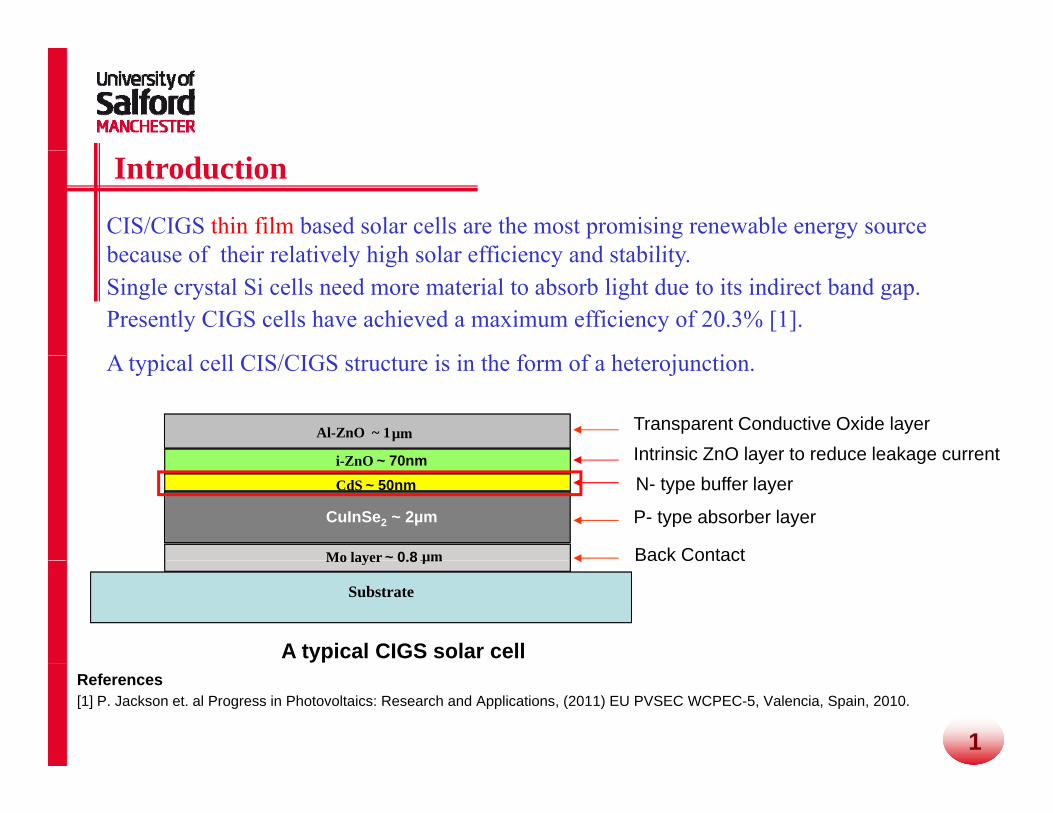
CIS/CIGS thin film based solar cells are the most promising renewable energy source because of their relatively high solar efficiency and stabilitybecause of their relatively high solar efficiency and stability. Single crystal Si cells need more material to absorb light due to its indirect band gap.Presently CIGS cells have achieved a maximum efficiency of 20.3% [1].
A i l ll CIS/CIGS i i h f f h j iA typical cell CIS/CIGS structure is in the form of a heterojunction.
i Z O 70nm
ZnO ~ 1?m
i Z O 70nm
Al-ZnO ~ 1µmIntrinsic ZnO layer to reduce leakage currentTransparent Conductive Oxide layer
Mo layer ~ 0.8? m
CuInSe2 ~ 1.0? m
CdS ~ 50nmi-ZnO ~ 70nm
Mo layer ~ 0.8
CdS ~ 50nmi-ZnO ~ 70nm
µm
CuInSe2 ~ 2µm
N- type buffer layerIntrinsic ZnO layer to reduce leakage current
P- type absorber layer
Back Contact
Substrate
Mo layer 0.8? m
Substrate
Mo layer 0.8 µm
A typical CIGS solar cell
Back Contact
1
References[1] P. Jackson et. al Progress in Photovoltaics: Research and Applications, (2011) EU PVSEC WCPEC-5, Valencia, Spain, 2010.
Introduction
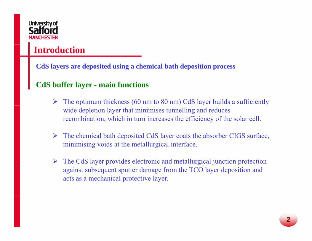
CdS layers are deposited using a chemical bath deposition process
CdS buffer layer - main functions
The optimum thickness (60 nm to 80 nm) CdS layer builds a sufficiently p ( ) y ywide depletion layer that minimises tunnelling and reduces recombination, which in turn increases the efficiency of the solar cell.
The chemical bath deposited CdS layer coats the absorber CIGS surfaceThe chemical bath deposited CdS layer coats the absorber CIGS surface, minimising voids at the metallurgical interface.
The CdS layer provides electronic and metallurgical junction protection against subsequent sputter damage from the TCO layer deposition and acts as a mechanical protective layer.
2
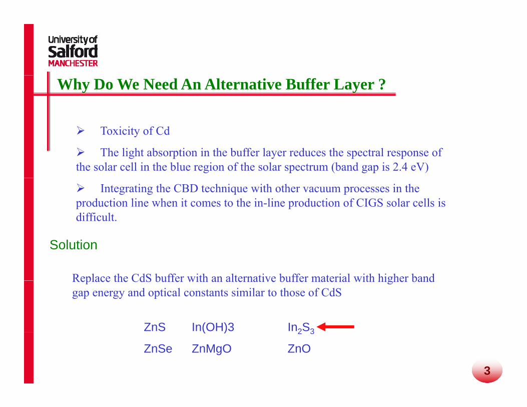
Why Do We Need An Alternative Buffer Layer ?
i i f CdToxicity of Cd
The light absorption in the buffer layer reduces the spectral response of the solar cell in the blue region of the solar spectrum (band gap is 2.4 eV)
Integrating the CBD technique with other vacuum processes in the production line when it comes to the in-line production of CIGS solar cells is difficult.
Solution
Replace the CdS buffer with an alternative buffer material with higher bandReplace the CdS buffer with an alternative buffer material with higher band gap energy and optical constants similar to those of CdS
ZnS In(OH)3 In2S3
3
( ) 2 3
ZnSe ZnMgO ZnO

Pulsed D.C. Magnetron Sputtering System
0 5 10 15 20 25 30 35 40 45 50 550
100
T (μs)
Pulse off
Substrate (Anode)K-type
Thermocouple
Substrate (Anode)K-type
Thermocouple
0 5 10 15 20 25 30 35 40 45 50 55
-300
-200
-100
Vol
tage
(V)
ArgonS/S* Cover
Camera
MFC100
sccm
p
ArgonS/S* Cover
Camera
MFC100
sccm
p
-500
-400
Pulse on
Ideal pulsed d.c signal for 100kHz
N NSCu -Target HolderMagnetsWater Channel
PTFE InsulatorS/S* Base
WindowN NS
Cu -Target HolderMagnetsWater Channel
PTFE InsulatorS/S* Base
Window
Water cooling
Turbo &Rotary pump
Substrate Heater
+
Ni-CrNi-Al
Water cooling
Turbo &Rotary pump
Substrate Heater
+
Ni-CrNi-Al
AE Pinnacle Plus Power Supply
Rotary pump+ -AE Pinnacle Plus
Power Supply
Rotary pump+ -
4ReferenceS. Karthikeyan et al, Vacuum, 2010, 85; pp.634-638.
In2S3 powder target
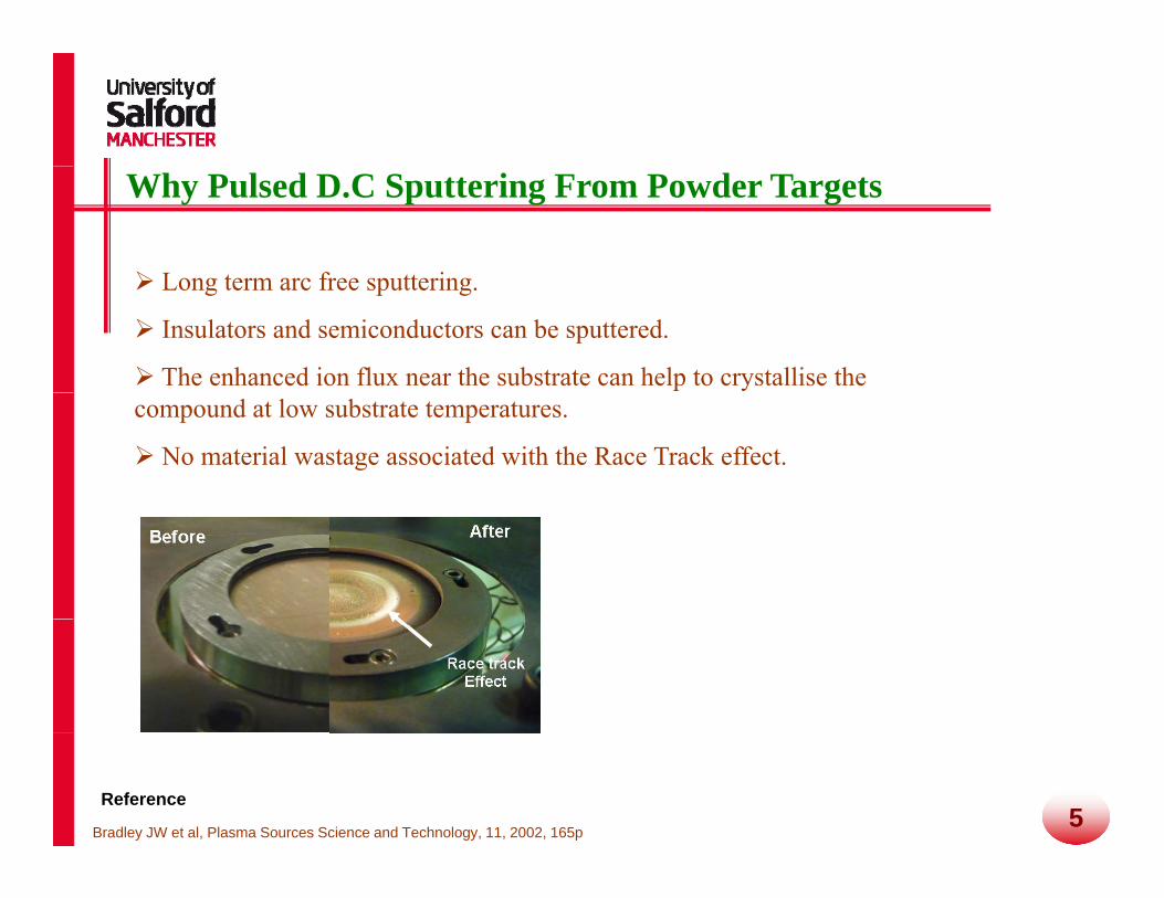
Why Pulsed D.C Sputtering From Powder Targets
Long term arc free sputteringLong term arc free sputtering.
Insulators and semiconductors can be sputtered.
The enhanced ion flux near the substrate can help to crystallise the compound at low substrate temperatures.
No material wastage associated with the Race Track effect.
Bradley JW et al, Plasma Sources Science and Technology, 11, 2002, 165p
Reference5
Materials Deposited
1 Molybdenum (back contact) [1]1. Molybdenum (back contact) [1]
2. Copper indium diselenide (absorber layer)[2]
3. Indium sulphide (buffer layer)
4. Indium oxide (Transparent Conductive Oxide layer)[3]
6
[1] S. Karthikeyan et al, Thin Solid Films, 2011, 250, pp.266-271.[2] S.Karthikeyan et al, Thin Solid Films, 2011, 519; pp.3107 -3112
[3] S.Karthikeyan et al,The effect of oxygen on the properties of pulsed d.c magnetron sputtered In2O3 films. in: 1st CSE
Postgraduate Conference 2010, University of Salford, United Kingdom.
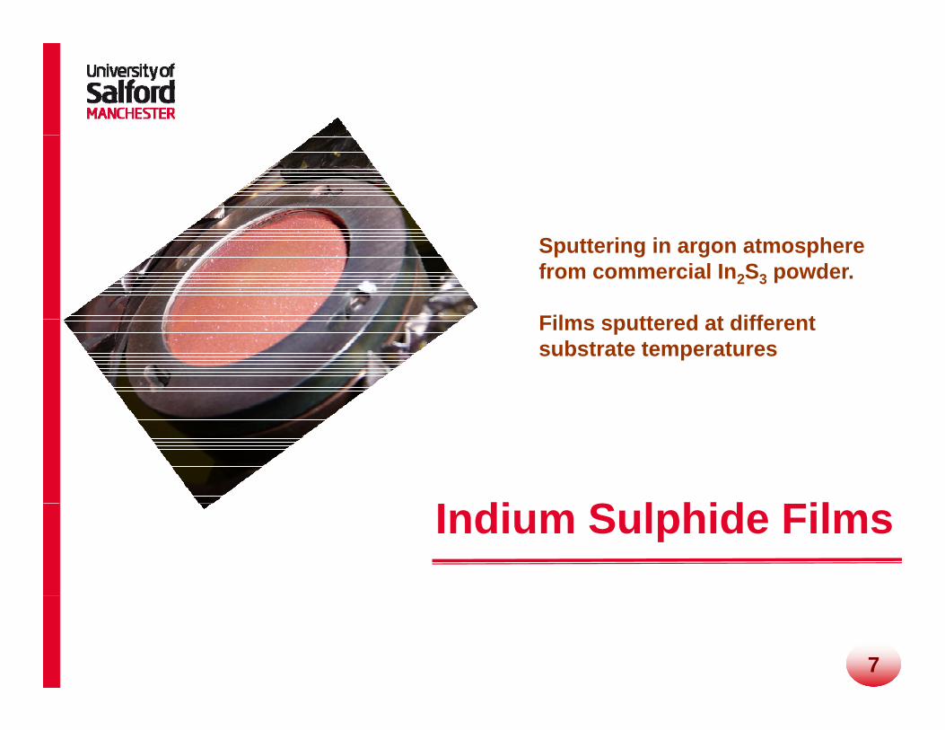
Sputtering in argon atmosphere from commercial In2S3 powder.
Films sputtered at differentFilms sputtered at different substrate temperatures
I di S l hid FilIndium Sulphide Films
7
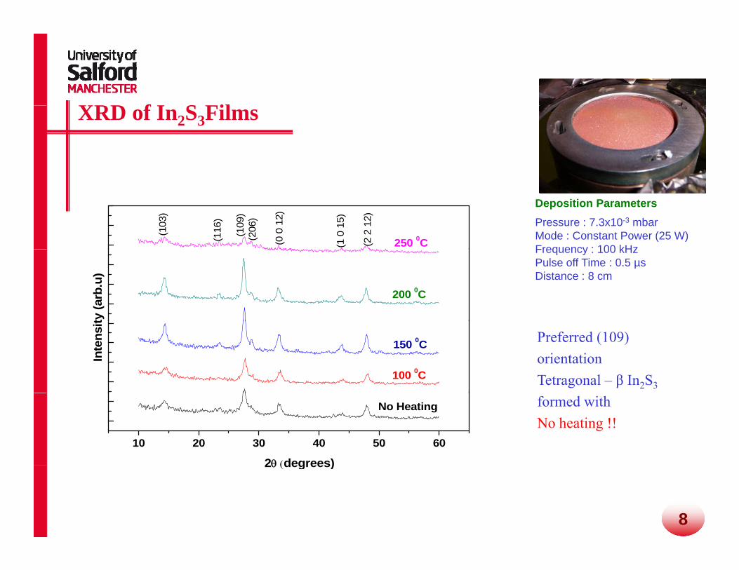
XRD f I S FilXRD of In2S3Films
Deposition ParametersPressure : 7.3x10⁻³ mbarMode : Constant Power (25 W)Frequency : 100 kHz(2
2 1
2)
(1 0
15)
(0 0
12)
(206
)(1
09)
250 0C
(103
)
(116
)
Frequency : 100 kHzPulse off Time : 0.5 µsDistance : 8 cm
200 0C
ty (a
rb.u
)
150 0C
100 0C
Inte
nsit
Preferred (109) orientationTetragonal – β In2S3
10 20 30 40 50 60
2θ (degrees)
No Heating formed withNo heating !!
2θ (degrees)
8
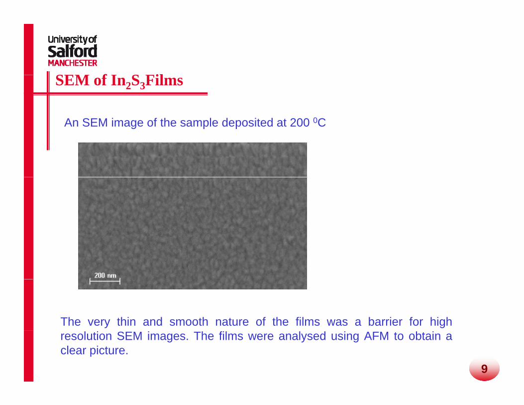
SEM f I S FilSEM of In2S3Films
An SEM image of the sample deposited at 200 0CAn SEM image of the sample deposited at 200 C
The very thin and smooth nature of the films was a barrier for highresolution SEM images. The films were analysed using AFM to obtain aclear picture.
9
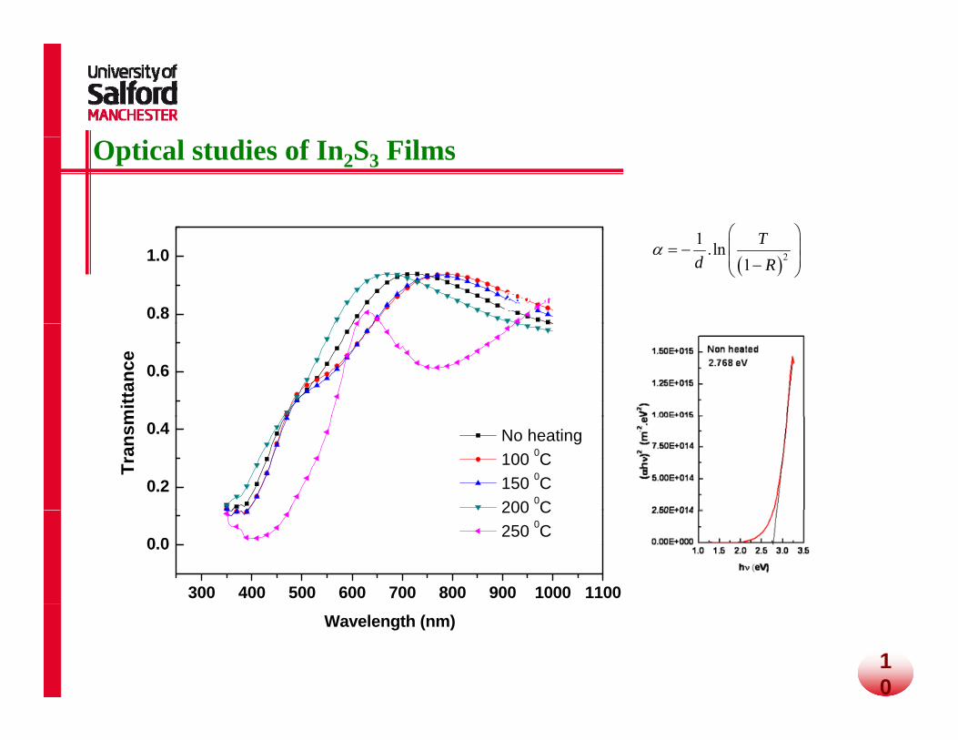
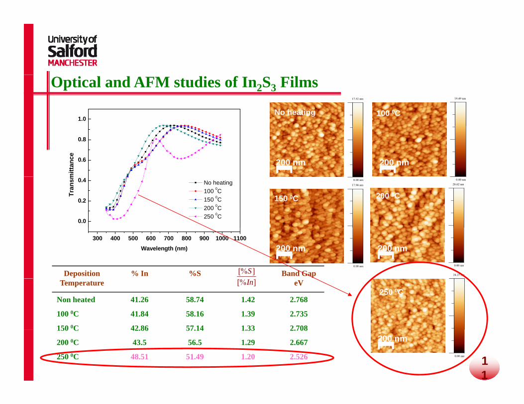
Optical studies of In2S3 Films
No heating 100 0C
⎛ ⎞
0.8
1.0
200 nm 200 nm
( )21 .ln
1T
d Rα
⎛ ⎞⎜ ⎟= −⎜ ⎟−⎝ ⎠
0.6
mitt
ance 150 0C
0.2
0.4
Tran
sm No heating 100 0C 150 0C200 0C
300 400 500 600 700 800 900 1000 1100
0.0
200 C 250 0C
Wavelength (nm)
10
200 nm
1.0
Optical and AFM studies of In2S3 Films17.52 nm
No heating
19.49 nm
100 0C
0.6
0.8
mitt
ance
200nm 200nm200 nm 200 nm
0.0
0.2
0.4
Tran
sm No heating 100 0C 150 0C 200 0C 250 0C
0.00 nm 0.00 nm
17.94 nm 28.62 nm
150 0C 200 0C
300 400 500 600 700 800 900 1000 1100Wavelength (nm)
Deposition % In %S Band Gap[% ]S0.00 nm
200nm
0.00 nm
200nm
24.27 nm
200 nm 200 nm
Temperature eV
Non heated 41.26 58.74 1.42 2.768
100 0C 41.84 58.16 1.39 2.735
150 0C 42.86 57.14 1.33 2.708
[% ]In250 0C
150 C 42.86 57.14 1.33 2.708
200 0C 43.5 56.5 1.29 2.667
250 0C 48.51 51.49 1.20 2.526 0.00 nm
200nm
11
200 nm
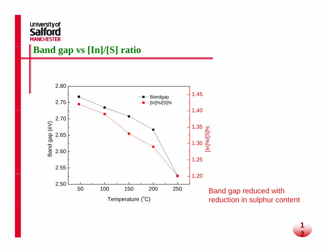
B d [I ]/[S] iBand gap vs [In]/[S] ratio
1 40
1.452.75
2.80
Bandgap [In]%/[S]%
1 30
1.35
1.40
2.65
2.70
gap
(eV)
%/[S
]%
1 20
1.25
1.30
2.55
2.60Band
g
[In]%
1.20
50 100 150 200 2502.50
Temperature (oC)Band gap reduced with reduction in sulphur content
12
Conclusions
The possibilities of pulsed d c magnetron sputtering for the deposition of In S andThe possibilities of pulsed d.c magnetron sputtering for the deposition of In2S3 andfilms from powdered targets were studied.
The XRD analysis revealed that the films are in single phase.
The room temperature sputtered In2S3 films showed a maximum band gap about 2.768 eV which is higher compared to reported single crystal value.
The higher band gap reduces the absorption in the blue region of the solar spectrum d i h l ll ffi iand can increase the solar cell efficiency.
The band gap of the In2S3 thin films reduced with sputtering temperature possibly due to the reduction in sulphur content.
A single process for all the layer can cut down the overall cost of production of the solar cell and use of an In2S3 buffer layer can produce Cd free solar cells
13

Acknowledgments
Prof . A. E. Hill , Materials and Physics Research Centre , University of Salford
Dr. R. D. Pilkington, Materials and Physics Research Centre , University of Salford
Dr. H. Yates, Materials and Physics Research Centre , University of Salford
Mr. G. Parr, Salford Analytical Services, University of Salford.
Ms. M. Hardacre, Salford Analytical Services, University of Salford.
Mr. J. Smith, Physics Technician , University of Salford.
Mr. M. Clegg, Physics Technician , University of Salford.
Finally , thanks to everybody who has indirectly helped to bring this work to fruition.
Thanks for your attention


![Annealing Temperature Effect on Properties of Chemically ... · thin films , such as vacuum evaporation [9,10], magnetron sputtering [11], molecular beam Epitaxy [12], pulsed laser](https://img.dokumen.tips/doc/110x75/6061d5e01f829d0789738fa2/annealing-temperature-effect-on-properties-of-chemically-thin-films-such-as.jpg)