Embed Size (px)
Citation preview

High power pulsed magnetron sputtering: A method to increase deposition ratePriya Raman, Ivan A. Shchelkanov, Jake McLain, and David N Ruzic Citation: Journal of Vacuum Science & Technology A 33, 031304 (2015); doi: 10.1116/1.4916108 View online: http://dx.doi.org/10.1116/1.4916108 View Table of Contents: http://scitation.aip.org/content/avs/journal/jvsta/33/3?ver=pdfcov Published by the AVS: Science & Technology of Materials, Interfaces, and Processing Articles you may be interested in Method to control deposition rate instabilities—High power impulse magnetron sputtering deposition of TiO2 J. Vac. Sci. Technol. A 33, 021514 (2015); 10.1116/1.4905737 Modified high power impulse magnetron sputtering process for increased deposition rate of titanium J. Vac. Sci. Technol. A 31, 060604 (2013); 10.1116/1.4819296 Effects of the magnetic field strength on the modulated pulsed power magnetron sputtering of metallic films J. Vac. Sci. Technol. A 29, 061301 (2011); 10.1116/1.3645612 On the deposition rate in a high power pulsed magnetron sputtering discharge Appl. Phys. Lett. 89, 154104 (2006); 10.1063/1.2362575 High-rate deposition of MgO by reactive ac pulsed magnetron sputtering in the transition mode J. Vac. Sci. Technol. A 24, 106 (2006); 10.1116/1.2138717
Redistribution subject to AVS license or copyright; see http://scitation.aip.org/termsconditions. Download to IP: 128.174.163.241 On: Tue, 31 Mar 2015 15:36:42
High power pulsed magnetron sputtering: A method to increasedeposition rate
Priya Ramana)
Center for Plasma Material Interactions, University of Illinois, Urbana, Illinois 61801
Ivan A. ShchelkanovCenter for Plasma Material Interactions, University of Illinois, Urbana, Illinois 61801 and National NuclearResearch University MEPhI (Moscow Engineering Physics Institute), Moscow 115409, Russia
Jake McLain and David N RuzicCenter for Plasma Material Interactions, University of Illinois, Urbana, Illinois 61801
(Received 10 October 2014; accepted 12 March 2015; published 25 March 2015)
High power pulsed magnetron sputtering (HPPMS) is a state-of-the-art physical vapor deposition
technique with several industrial applications. One of the main disadvantages of this process is its
low deposition rate. In this work, the authors report a new magnetic field configuration, which
produces deposition rates twice that of conventional magnetron’s dipole magnetic field
configuration. Three different magnet pack configurations are discussed in this paper, and an
optimized magnet pack configuration for HPPMS that leads to a higher deposition rate and nearly
full-face target erosion is presented. The discussed magnetic field produced by a specially designed
magnet assembly is of the same size as the conventional magnet assembly and requires no external
fields. Comparison of deposition rates with different power supplies and the electron trapping
efficiency in complex magnetic field arrangements are discussed. VC 2015 American Vacuum Society.
[http://dx.doi.org/10.1116/1.4916108]
I. INTRODUCTION
Physical vapor deposition (PVD) techniques dominate the
thin film coating industry and the need for high quality coat-
ings is continuing to increase. Magnetron sputtering is one
of the most widely used PVD techniques. The magnetic field
configuration above the target allows one to obtain a higher
and stable discharge current at lower pressures than in a
normal glow discharge. The cylindrical symmetry of the
conventional planar magnetron gives rise to an arch shaped
magnetic field configuration above the target surface. In this
paper, the arch shaped magnetic field configuration will be
referred to as “conventional” design. This design was devel-
oped 30 years ago and the direct current (DC) charges in it
have been studied since then.1 Ionized PVD (iPVD) is a class
of PVD technique in which >50% of the deposition flux
may be ionized.2 Since ion energy and direction is easy to
control, iPVD techniques are used in a wide variety of appli-
cations like the formation of diffusion barriers and seed
layers on the side and bottom of high aspect ratio trenches
and vias in the microelectronics industry, enhancing
substrate pretreatment to improve adhesion of hard coatings,
depositing wear and corrosion resistant coatings, etc.3
High power pulsed magnetron sputtering (HPPMS) is a
type of iPVD technique where short high-peak-power (up to
3 kW/cm2) pulses are applied to the magnetron sputter target
at low duty cycles (0.5%–10%). HPPMS discharges can be
operated in the conventional magnet pack. This results in
plasma electron densities as high as 1019 m�3 above the
target surface during the short high-power pulses.4,5 These
high electron densities near the target enhance ionization of
sputtered materials.6 The now-ionized sputtered material is
accelerated back to the target resulting in an increase in the
sputtering rate by having the discharge go into a self-
sputtering mode.7 Some sputtered ions escape and provide
superior deposited film quality on the substrate. Electron
trapping efficiency and magnetic field influence on the
plasma potential distribution will be discussed later in the
paper. The films that are grown using HPPMS technique are
denser, smoother, and have better adhesion to the substrate
than the films deposited by direct current magnetron sputter-
ing (dcMS).8
Mozgrin et al.,9 first reported on a high power pulsed
magnetron discharge with pulse deposition rates no less than
80 lm/min at a distance of 120 mm from the cathode with 2
kJ pulse energy. Following this, a highly cited publication
by Kouznetsov et al.,6 reported that the deposition rate of
HPPMS was 80% lower than dcMS with high frequency low
energy pulses. Since then, deposition rates for different tar-
get materials were compared in dcMS and high power
impulse magnetron sputtering (HiPIMS) discharges for the
same average power by Samuelsson et al.10 The HiPIMS
deposition rates were consistently lower for all the target
materials. In the case of aluminum targets, the deposition
rate in HiPIMS was only 50% of dcMS rate.
Within the last decade, the scientific community came to
a conclusion that there are several reasons for the lower dep-
osition rates in HPPMS. The major one being metal ion
“return effect.” In HPPMS discharges, large fraction of sput-
tered atoms is ionized due to the dense plasma in front of the
target. Some of these newly formed ions return to the target
contributing to current increase and cause self-sputtering.11
The sputtered material is ionized close to the target, and the
negative potential applied on the target can extend far intoa)Electronic mail: [email protected]
031304-1 J. Vac. Sci. Technol. A 33(3), May/Jun 2015 0734-2101/2015/33(3)/031304/10/$30.00 VC 2015 American Vacuum Society 031304-1
Redistribution subject to AVS license or copyright; see http://scitation.aip.org/termsconditions. Download to IP: 128.174.163.241 On: Tue, 31 Mar 2015 15:36:42
the plasma as an extended presheath. In some unbalanced
magnetron cases, 10%–20% of the total applied voltage
drops in the magnetic presheath, which can extend to 40 mm
from the target.12 Hence, many of the metal ions will be
attracted back to the target surface by the cathode poten-
tial.13 Some of other reasons are yield effect,14 ion species
effect,11 magnetic unbalancing and guiding effect,15 and an
effect in which large fraction of ions of the sputtered
material are transported sideways.16 All named effects are
interconnected in HPPMS discharges and have a strong cor-
relation with the plasma parameters. Individual contribution
of the effect is hard to quantify and it depends on the mag-
netic field configuration on the target surface, HPPMS
pulsing power supply regime, geometry, etc. For example,
Mishra et al.17 reported that with a reduction of magnetic
field by 33% at the target surface, the deposition rate of
titanium increased by a factor of 6. To summarize, once the
HPPMS discharge gets to a state with a high fraction of ion-
ized sputtered material, the electric field distribution inside
the plasma prevents ions from escaping the plasma region.
The plasma electric potential during the discharge controls
the movement of ions, this means the electric potential distri-
bution in plasma during the discharge has to be controlled or
at least modified to increase the ion flow away from this
trap. There are publications18 that describe the relationship
between magnetic field topology and electric potential distri-
bution inside the plasma. Several attempts to investigate the
influence of magnetic field on HPPMS parameters were
done previously and can be summarized as follows: in case
of reduced magnetic field strength the ion flux toward the
substrate is increased due to the reduction in the metal ions
return effect in front of the target.19–21
A forerunner to the work presented here increased the
deposition rate by producing a magnetic field, which would
allow ions to leave the ionization region and move toward
the substrate without being recycled. This idea was tested
using a “spiral” magnet pack designed by Yu et al.22 This
work was continued by shrinking of the 14 in. design to fit
into Kurt J. Lesker’s 4 in. TORUS magnetron sputter source.
It will be shown in this work that simple scaling will not
work, and that further physics existed, and alternative design
rules have to be implemented in case of smaller magnetron
sputter guns.
II. EXPERIMENTAL SETUP
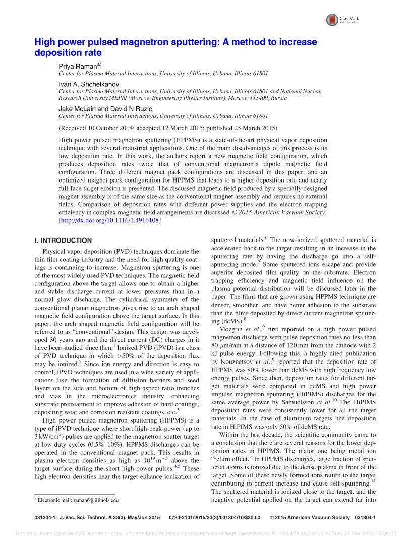
Sputtering high-purity atomic deposition experiment
(SHADE)23 is a dual magnetron setup for depositing thin
films under an ultrahigh vacuum environment. The SHADE
chamber [Fig. 1(a)] is equipped with a load lock for sample
transfer and a rotatable substrate holder for increasing the
uniformity of deposition, the substrate holder can be biased
if necessary. A pair of Kurt J. Lesker’s 4 in. TORUS magne-
tron sputter sources was installed in the SHADE chamber for
this work. In this manner, two different magnetic configura-
tions can literally be tested side-by-side keeping all other
FIG. 1. (Color online) (a) Schematic diagram of the SHADE chamber. (b) Schematic of the 4 in. silicon substrate location with respect to the target. (c)
Location of the uniformity test on the 4 in. silicon substrate.
031304-2 Raman et al.: High power pulsed magnetron sputtering 031304-2
J. Vac. Sci. Technol. A, Vol. 33, No. 3, May/Jun 2015
Redistribution subject to AVS license or copyright; see http://scitation.aip.org/termsconditions. Download to IP: 128.174.163.241 On: Tue, 31 Mar 2015 15:36:42
parameters identical. A number of different power supplies
were used in this work. An advanced energy pinnacle plus
was used for DC and pulsed DC sputtering, for HPPMS, a
Huttinger TruPlasma Highpulse 4002 was used (and will be
referred to as HiPIMS for high power impulse magnetron
sputtering), and a Zpulser Zpulser Cyprium VI was used
(and will be referred to as MPP for modulated pulse power
sputtering). The stainless steel vacuum chamber is pumped
by oil free vacuum pumps to a base pressure of
1� 10�7 Torr. Gas flow into the chamber is controlled by
mass flow controllers.
For in-situ measurements of deposited film thickness, the
SHADE chamber was equipped with an Inficon DLAE47
quartz crystal microbalance (QCM). The location of the
QCM is as shown in Figs. 1(b) and 1(c). It was positioned
equidistant between the two magnetrons. To increase the
accuracy of the QCM, two QCMs (one for control and the
other one for actual measurements) were used simultane-
ously at the same location. Control QCM is masked with a
stainless steel shim stock to subtract the noise from thermal
drift.
To verify the QCM deposition rate measurement accuracy
during HPPMS discharge operation, a half masked test wafer
was placed in the actual QCM location. The deposited film
thickness on the test wafer was measured using a DEKTAK
3030 surface profilometer and it was compared to the QCM
thickness readings. The QCM measurement difference
between the two techniques was found to be less than 2%.
Aluminum targets were used in all the experiments. For the
“e” magnet pack, which is described later in the paper, a
graded-thickness aluminum target was used. The outer rim
of the graded aluminum target was 0.125 in. thick and the
inner portion was 0.09 in. thick. This design was chosen to
sustain a stable HPPMS discharge with the premanufactured
magnet set. Slightly stronger magnets in the inner e portion
of the epsilon pack would eliminate the need to use a graded
target.
III. MAGNET PACK DESIGN AND SIMULATION
In this work, a one-to-one scale 3D model was built in
COMSOL Multiphysics finite element analysis software to
simulate the magnetic field pattern and electron trajectories
above target surface. The “magnetic and electric field”
module of COMSOL Multiphysics was used to calculate the
magnetic flux densities and B//¼ (ffiffiffiffiffiffiffiffiffiffiffiffiffiffiffiffiB2
x þ B2y
q), XY plane is
parallel to the target surface) for any given magnet pack
arrangement. The distribution of B// above target allows to
predict the racetrack region.19 Charged particle tracing
(CPT) module was used to simulate the electron trajectories
above the target surface. Average electron temperatures in
HiPIMS discharges are in the order of 0.3–0.4 eV at 20
mTorr.24 In the CPT module, electrons are injected into the
race-track on the target surface with energy of 0.1 eV, which
is in the range of the average electron energy. This module
takes into account electron to electron interaction and parti-
cle to field interaction. Total number of particles in a single
run is 1000. In every simulation, electrons are released at
time step zero and the CPT module resolves particle position
at every 0.1 ns. This model for particle tracing is a simplistic
way to visualize single particle trajectories and is not
intended to directly describe physical phenomena in HPPMS
discharge. Scattering and the Hall current are ignored.
However, it allows reconstructing a general behavior of elec-
trons in the trap.
A. Conventional magnet pack
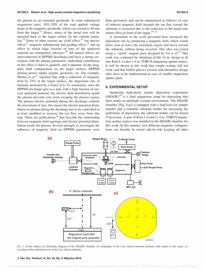
A commercially available 4 in. magnetron sputter gun is
equipped with a concentric magnet assembly, which gives
rise to a circular race track on the target surface. Figure 2(a)
shows the shape and magnitude of B// field on the XY plane
of the target surface. X and Y axes represent the physical
dimension in inches of the target. Figure 2(b) shows the
streamline plot of magnetic field lines in XZ plane, Bx and
Bz (magnetic field component along x and z directions) of
the conventional magnet pack.
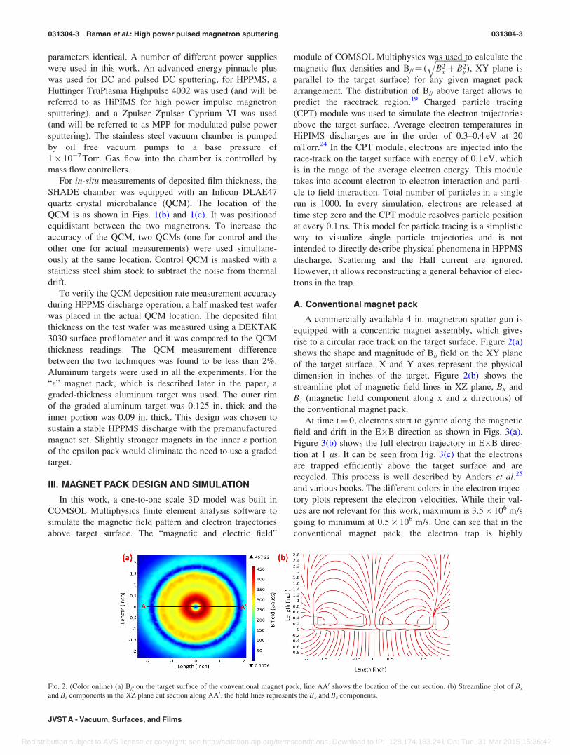
At time t¼ 0, electrons start to gyrate along the magnetic
field and drift in the E�B direction as shown in Figs. 3(a).
Figure 3(b) shows the full electron trajectory in E�B direc-
tion at 1 ls. It can be seen from Fig. 3(c) that the electrons
are trapped efficiently above the target surface and are
recycled. This process is well described by Anders et al.25
and various books. The different colors in the electron trajec-
tory plots represent the electron velocities. While their val-
ues are not relevant for this work, maximum is 3.5� 106 m/s
going to minimum at 0.5� 106 m/s. One can see that in the
conventional magnet pack, the electron trap is highly
FIG. 2. (Color online) (a) B// on the target surface of the conventional magnet pack, line AA0 shows the location of the cut section. (b) Streamline plot of Bx
and Bz components in the XZ plane cut section along AA0, the field lines represents the Bx and Bz components.
031304-3 Raman et al.: High power pulsed magnetron sputtering 031304-3
JVST A - Vacuum, Surfaces, and Films
Redistribution subject to AVS license or copyright; see http://scitation.aip.org/termsconditions. Download to IP: 128.174.163.241 On: Tue, 31 Mar 2015 15:36:42
efficient, which in turn makes the HPPMS ion recycling pro-
cess also very efficient.
B. Spiral magnet pack
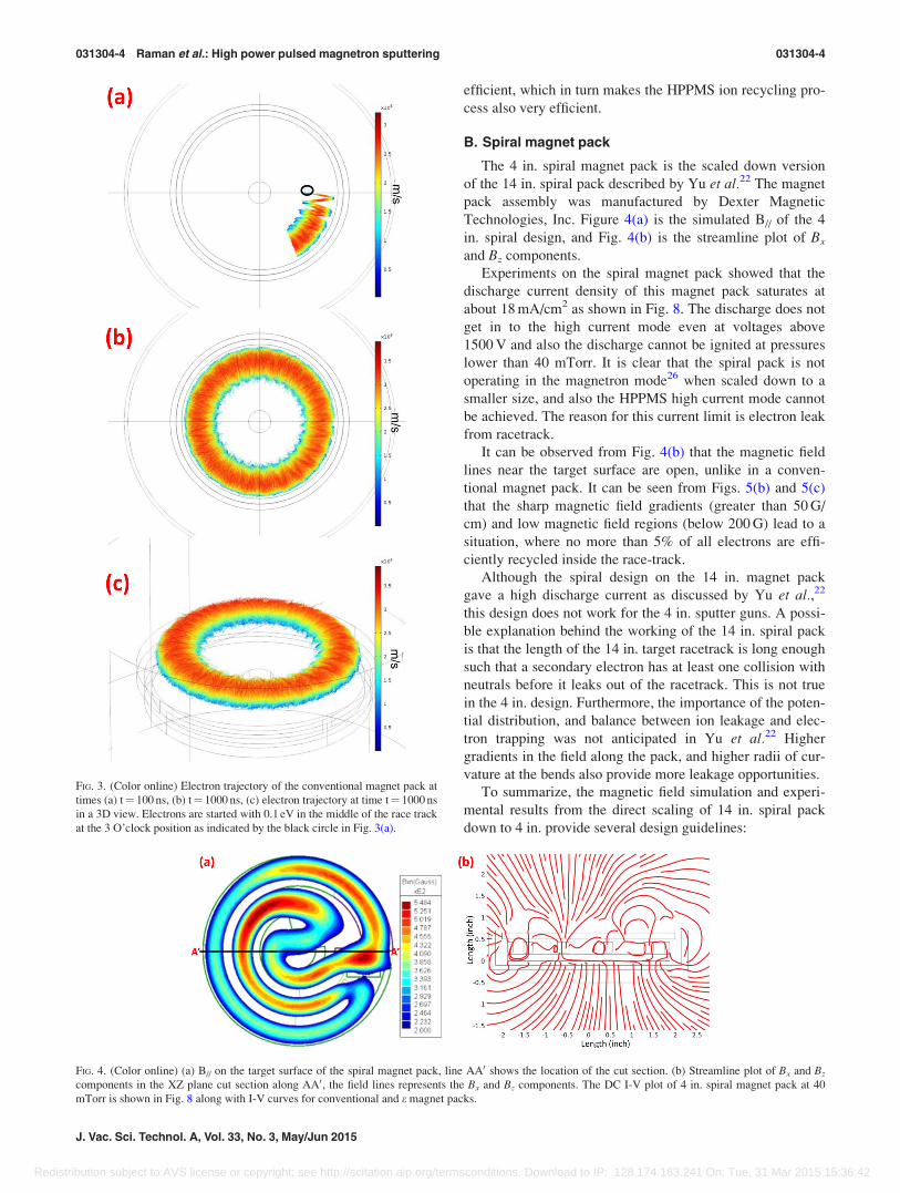
The 4 in. spiral magnet pack is the scaled down version
of the 14 in. spiral pack described by Yu et al.22 The magnet
pack assembly was manufactured by Dexter Magnetic
Technologies, Inc. Figure 4(a) is the simulated B// of the 4
in. spiral design, and Fig. 4(b) is the streamline plot of Bx
and Bz components.
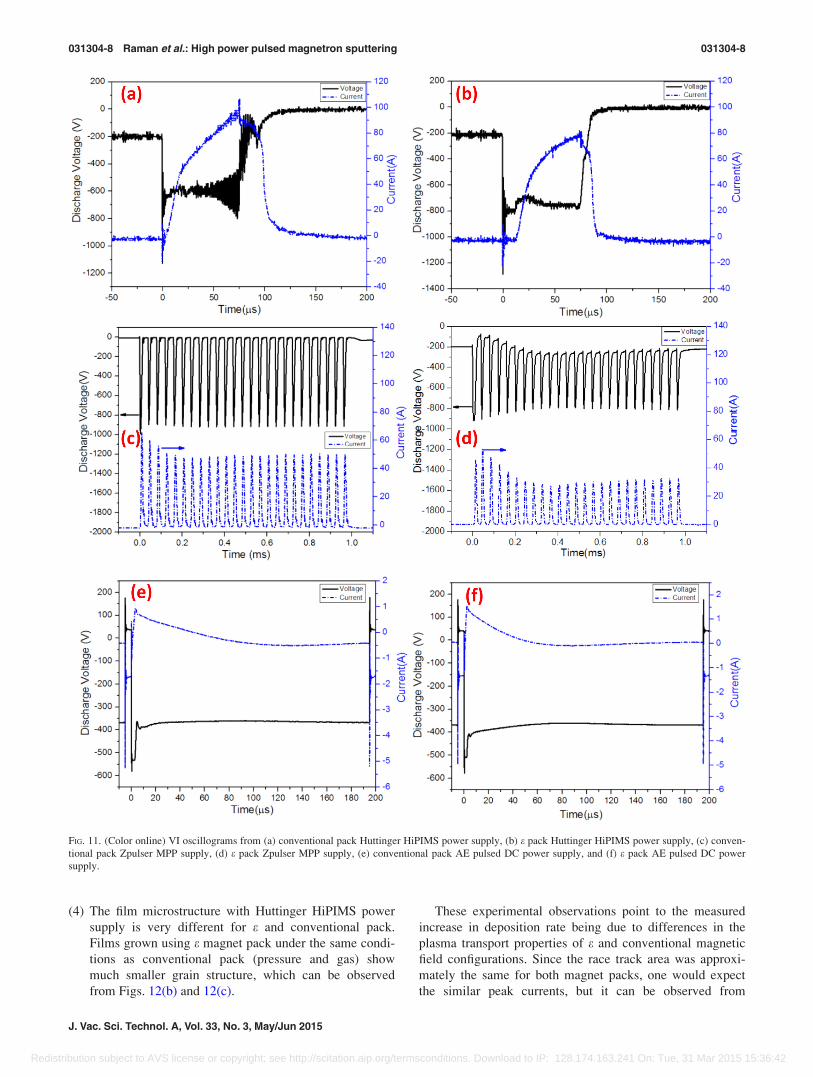
Experiments on the spiral magnet pack showed that the
discharge current density of this magnet pack saturates at
about 18 mA/cm2 as shown in Fig. 8. The discharge does not
get in to the high current mode even at voltages above
1500 V and also the discharge cannot be ignited at pressures
lower than 40 mTorr. It is clear that the spiral pack is not
operating in the magnetron mode26 when scaled down to a
smaller size, and also the HPPMS high current mode cannot
be achieved. The reason for this current limit is electron leak
from racetrack.
It can be observed from Fig. 4(b) that the magnetic field
lines near the target surface are open, unlike in a conven-
tional magnet pack. It can be seen from Figs. 5(b) and 5(c)
that the sharp magnetic field gradients (greater than 50 G/
cm) and low magnetic field regions (below 200 G) lead to a
situation, where no more than 5% of all electrons are effi-
ciently recycled inside the race-track.
Although the spiral design on the 14 in. magnet pack
gave a high discharge current as discussed by Yu et al.,22
this design does not work for the 4 in. sputter guns. A possi-
ble explanation behind the working of the 14 in. spiral pack
is that the length of the 14 in. target racetrack is long enough
such that a secondary electron has at least one collision with
neutrals before it leaks out of the racetrack. This is not true
in the 4 in. design. Furthermore, the importance of the poten-
tial distribution, and balance between ion leakage and elec-
tron trapping was not anticipated in Yu et al.22 Higher
gradients in the field along the pack, and higher radii of cur-
vature at the bends also provide more leakage opportunities.
To summarize, the magnetic field simulation and experi-
mental results from the direct scaling of 14 in. spiral pack
down to 4 in. provide several design guidelines:
FIG. 3. (Color online) Electron trajectory of the conventional magnet pack at
times (a) t¼ 100 ns, (b) t¼ 1000 ns, (c) electron trajectory at time t¼ 1000 ns
in a 3D view. Electrons are started with 0.1 eV in the middle of the race track
at the 3 O’clock position as indicated by the black circle in Fig. 3(a).
FIG. 4. (Color online) (a) B// on the target surface of the spiral magnet pack, line AA0 shows the location of the cut section. (b) Streamline plot of Bx and Bz
components in the XZ plane cut section along AA0, the field lines represents the Bx and Bz components. The DC I-V plot of 4 in. spiral magnet pack at 40
mTorr is shown in Fig. 8 along with I-V curves for conventional and e magnet packs.
031304-4 Raman et al.: High power pulsed magnetron sputtering 031304-4
J. Vac. Sci. Technol. A, Vol. 33, No. 3, May/Jun 2015
Redistribution subject to AVS license or copyright; see http://scitation.aip.org/termsconditions. Download to IP: 128.174.163.241 On: Tue, 31 Mar 2015 15:36:42
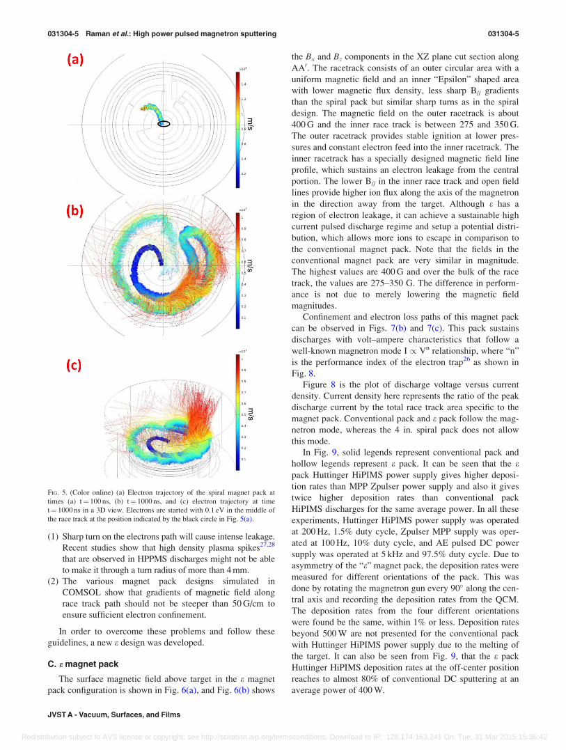
(1) Sharp turn on the electrons path will cause intense leakage.
Recent studies show that high density plasma spikes27,28
that are observed in HPPMS discharges might not be able
to make it through a turn radius of more than 4 mm.
(2) The various magnet pack designs simulated in
COMSOL show that gradients of magnetic field along
race track path should not be steeper than 50 G/cm to
ensure sufficient electron confinement.
In order to overcome these problems and follow these
guidelines, a new e design was developed.
C. e magnet pack
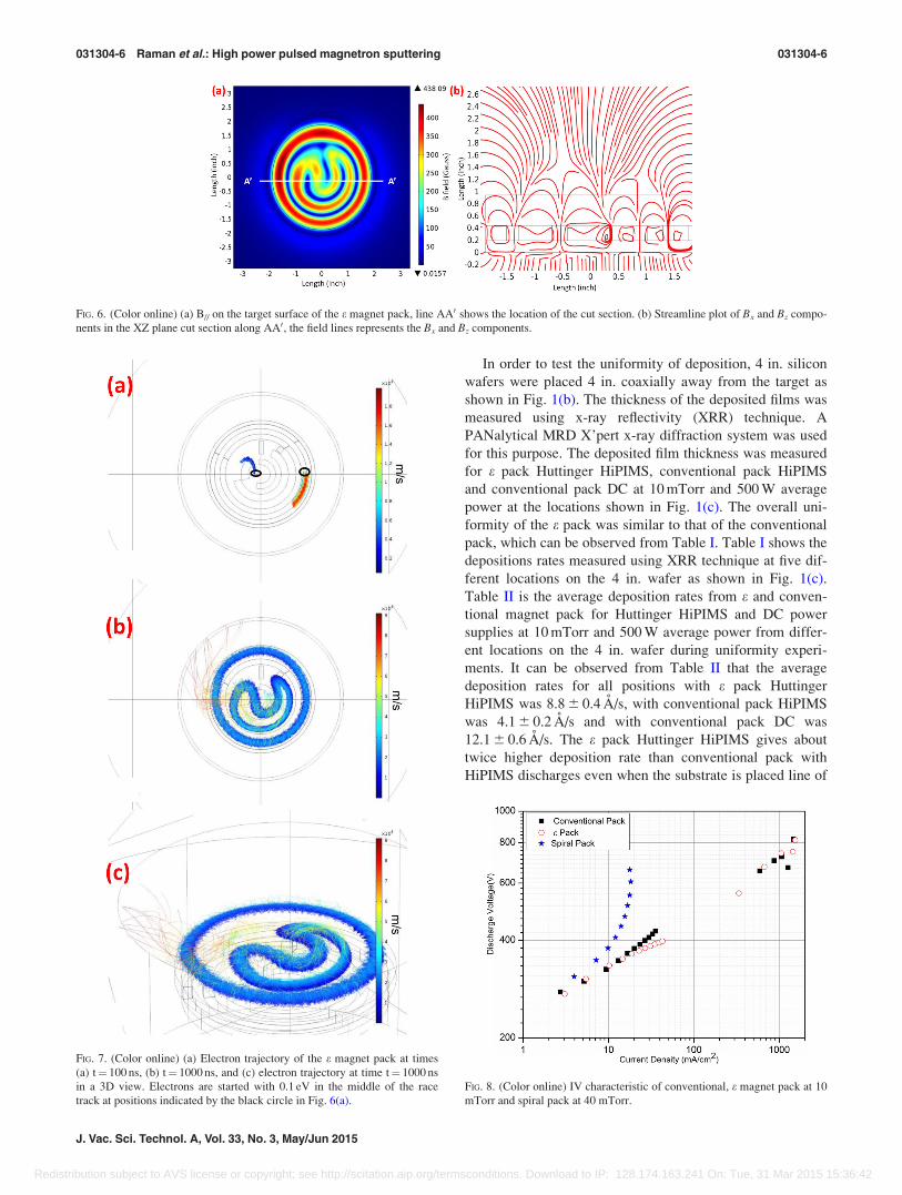
The surface magnetic field above target in the e magnet
pack configuration is shown in Fig. 6(a), and Fig. 6(b) shows
the Bx and Bz components in the XZ plane cut section along
AA0. The racetrack consists of an outer circular area with a
uniform magnetic field and an inner “Epsilon” shaped area
with lower magnetic flux density, less sharp B// gradients
than the spiral pack but similar sharp turns as in the spiral
design. The magnetic field on the outer racetrack is about
400 G and the inner race track is between 275 and 350 G.
The outer racetrack provides stable ignition at lower pres-
sures and constant electron feed into the inner racetrack. The
inner racetrack has a specially designed magnetic field line
profile, which sustains an electron leakage from the central
portion. The lower B// in the inner race track and open field
lines provide higher ion flux along the axis of the magnetron
in the direction away from the target. Although e has a
region of electron leakage, it can achieve a sustainable high
current pulsed discharge regime and setup a potential distri-
bution, which allows more ions to escape in comparison to
the conventional magnet pack. Note that the fields in the
conventional magnet pack are very similar in magnitude.
The highest values are 400 G and over the bulk of the race
track, the values are 275–350 G. The difference in perform-
ance is not due to merely lowering the magnetic field
magnitudes.
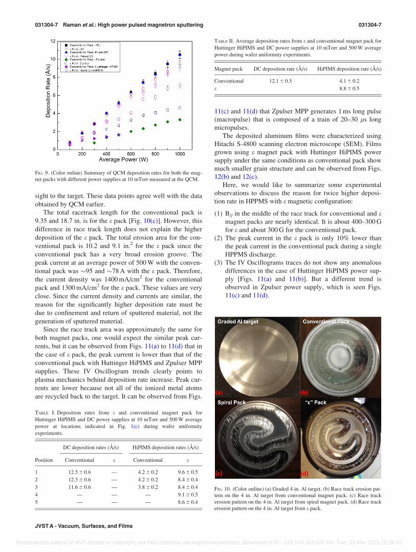
Confinement and electron loss paths of this magnet pack
can be observed in Figs. 7(b) and 7(c). This pack sustains
discharges with volt–ampere characteristics that follow a
well-known magnetron mode I / Vn relationship, where “n”
is the performance index of the electron trap26 as shown in
Fig. 8.
Figure 8 is the plot of discharge voltage versus current
density. Current density here represents the ratio of the peak
discharge current by the total race track area specific to the
magnet pack. Conventional pack and e pack follow the mag-
netron mode, whereas the 4 in. spiral pack does not allow
this mode.
In Fig. 9, solid legends represent conventional pack and
hollow legends represent e pack. It can be seen that the epack Huttinger HiPIMS power supply gives higher deposi-
tion rates than MPP Zpulser power supply and also it gives
twice higher deposition rates than conventional pack
HiPIMS discharges for the same average power. In all these
experiments, Huttinger HiPIMS power supply was operated
at 200 Hz, 1.5% duty cycle, Zpulser MPP supply was oper-
ated at 100 Hz, 10% duty cycle, and AE pulsed DC power
supply was operated at 5 kHz and 97.5% duty cycle. Due to
asymmetry of the “e” magnet pack, the deposition rates were
measured for different orientations of the pack. This was
done by rotating the magnetron gun every 90� along the cen-
tral axis and recording the deposition rates from the QCM.
The deposition rates from the four different orientations
were found be the same, within 1% or less. Deposition rates
beyond 500 W are not presented for the conventional pack
with Huttinger HiPIMS power supply due to the melting of
the target. It can also be seen from Fig. 9, that the e pack
Huttinger HiPIMS deposition rates at the off-center position
reaches to almost 80% of conventional DC sputtering at an
average power of 400 W.
FIG. 5. (Color online) (a) Electron trajectory of the spiral magnet pack at
times (a) t¼ 100 ns, (b) t¼ 1000 ns, and (c) electron trajectory at time
t¼ 1000 ns in a 3D view. Electrons are started with 0.1 eV in the middle of
the race track at the position indicated by the black circle in Fig. 5(a).
031304-5 Raman et al.: High power pulsed magnetron sputtering 031304-5
JVST A - Vacuum, Surfaces, and Films
Redistribution subject to AVS license or copyright; see http://scitation.aip.org/termsconditions. Download to IP: 128.174.163.241 On: Tue, 31 Mar 2015 15:36:42
In order to test the uniformity of deposition, 4 in. silicon
wafers were placed 4 in. coaxially away from the target as
shown in Fig. 1(b). The thickness of the deposited films was
measured using x-ray reflectivity (XRR) technique. A
PANalytical MRD X’pert x-ray diffraction system was used
for this purpose. The deposited film thickness was measured
for e pack Huttinger HiPIMS, conventional pack HiPIMS
and conventional pack DC at 10 mTorr and 500 W average
power at the locations shown in Fig. 1(c). The overall uni-
formity of the e pack was similar to that of the conventional
pack, which can be observed from Table I. Table I shows the
depositions rates measured using XRR technique at five dif-
ferent locations on the 4 in. wafer as shown in Fig. 1(c).
Table II is the average deposition rates from e and conven-
tional magnet pack for Huttinger HiPIMS and DC power
supplies at 10 mTorr and 500 W average power from differ-
ent locations on the 4 in. wafer during uniformity experi-
ments. It can be observed from Table II that the average
deposition rates for all positions with e pack Huttinger
HiPIMS was 8.8 6 0.4 A/s, with conventional pack HiPIMS
was 4.1 6 0.2 A/s and with conventional pack DC was
12.1 6 0.6 A/s. The e pack Huttinger HiPIMS gives about
twice higher deposition rate than conventional pack with
HiPIMS discharges even when the substrate is placed line of
FIG. 6. (Color online) (a) B// on the target surface of the e magnet pack, line AA0 shows the location of the cut section. (b) Streamline plot of Bx and Bz compo-
nents in the XZ plane cut section along AA0, the field lines represents the Bx and Bz components.
FIG. 7. (Color online) (a) Electron trajectory of the e magnet pack at times
(a) t¼ 100 ns, (b) t¼ 1000 ns, and (c) electron trajectory at time t¼ 1000 ns
in a 3D view. Electrons are started with 0.1 eV in the middle of the race
track at positions indicated by the black circle in Fig. 6(a).
FIG. 8. (Color online) IV characteristic of conventional, e magnet pack at 10
mTorr and spiral pack at 40 mTorr.
031304-6 Raman et al.: High power pulsed magnetron sputtering 031304-6
J. Vac. Sci. Technol. A, Vol. 33, No. 3, May/Jun 2015
Redistribution subject to AVS license or copyright; see http://scitation.aip.org/termsconditions. Download to IP: 128.174.163.241 On: Tue, 31 Mar 2015 15:36:42
sight to the target. These data points agree well with the data
obtained by QCM earlier.
The total racetrack length for the conventional pack is
9.35 and 18.7 in. is for the e pack [Fig. 10(c)]. However, this
difference in race track length does not explain the higher
deposition of the e pack. The total erosion area for the con-
ventional pack is 10.2 and 9.1 in.2 for the e pack since the
conventional pack has a very broad erosion groove. The
peak current at an average power of 500 W with the conven-
tional pack was �95 and �78 A with the e pack. Therefore,
the current density was 1400 mA/cm2 for the conventional
pack and 1300 mA/cm2 for the e pack. These values are very
close. Since the current density and currents are similar, the
reason for the significantly higher deposition rate must be
due to confinement and return of sputtered material, not the
generation of sputtered material.
Since the race track area was approximately the same for
both magnet packs, one would expect the similar peak cur-
rents, but it can be observed from Figs. 11(a) to 11(d) that in
the case of e pack, the peak current is lower than that of the
conventional pack with Huttinger HiPIMS and Zpulser MPP
supplies. These IV Oscillogram trends clearly points to
plasma mechanics behind deposition rate increase. Peak cur-
rents are lower because not all of the ionized metal atoms
are recycled back to the target. It can be observed from Figs.
11(c) and 11(d) that Zpulser MPP generates 1 ms long pulse
(macropulse) that is composed of a train of 20–30 ls long
micropulses.
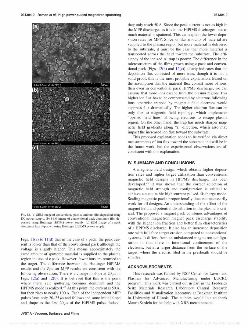
The deposited aluminum films were characterized using
Hitachi S-4800 scanning electron microscope (SEM). Films
grown using e magnet pack with Huttinger HiPIMS power
supply under the same conditions as conventional pack show
much smaller grain structure and can be observed from Figs.
12(b) and 12(c).
Here, we would like to summarize some experimental
observations to discuss the reason for twice higher deposi-
tion rate in HPPMS with e magnetic configuration:
(1) B// in the middle of the race track for conventional and emagnet packs are nearly identical. It is about 400–300 G
for e and about 300 G for the conventional pack.
(2) The peak current in the e pack is only 10% lower than
the peak current in the conventional pack during a single
HPPMS discharge.
(3) The IV Oscillograms traces do not show any anomalous
differences in the case of Huttinger HiPIMS power sup-
ply [Figs. 11(a) and 11(b)]. But a different trend is
observed in Zpulser power supply, which is seen Figs.
11(c) and 11(d).
FIG. 9. (Color online) Summary of QCM deposition rates for both the mag-
net packs with different power supplies at 10 mTorr measured at the QCM.
TABLE I. Deposition rates from e and conventional magnet pack for
Huttinger HiPIMS and DC power supplies at 10 mTorr and 500 W average
power at locations indicated in Fig. 1(c) during wafer uniformity
experiments.
Position
DC deposition rates (A/s) HiPIMS deposition rates (A/s)
Conventional e Conventional e
1 12.5 6 0.6 — 4.2 6 0.2 9.6 6 0.5
2 12.3 6 0.6 — 4.2 6 0.2 8.4 6 0.4
3 11.6 6 0.6 — 3.8 6 0.2 8.4 6 0.4
4 — — — 9.1 6 0.5
5 — — — 8.6 6 0.4
TABLE II. Average deposition rates from e and conventional magnet pack for
Huttinger HiPIMS and DC power supplies at 10 mTorr and 500 W average
power during wafer uniformity experiments.
Magnet pack DC deposition rate (A/s) HiPIMS deposition rate (A/s)
Conventional 12.1 6 0.5 4.1 6 0.2
e 8.8 6 0.5
FIG. 10. (Color online) (a) Graded 4 in. Al target. (b) Race track erosion pat-
tern on the 4 in. Al target from conventional magnet pack. (c) Race track
erosion pattern on the 4 in. Al target from spiral magnet pack. (d) Race track
erosion pattern on the 4 in. Al target from e pack.
031304-7 Raman et al.: High power pulsed magnetron sputtering 031304-7
JVST A - Vacuum, Surfaces, and Films
Redistribution subject to AVS license or copyright; see http://scitation.aip.org/termsconditions. Download to IP: 128.174.163.241 On: Tue, 31 Mar 2015 15:36:42
(4) The film microstructure with Huttinger HiPIMS power
supply is very different for e and conventional pack.
Films grown using e magnet pack under the same condi-
tions as conventional pack (pressure and gas) show
much smaller grain structure, which can be observed
from Figs. 12(b) and 12(c).
These experimental observations point to the measured
increase in deposition rate being due to differences in the
plasma transport properties of e and conventional magnetic
field configurations. Since the race track area was approxi-
mately the same for both magnet packs, one would expect
the similar peak currents, but it can be observed from
FIG. 11. (Color online) VI oscillograms from (a) conventional pack Huttinger HiPIMS power supply, (b) e pack Huttinger HiPIMS power supply, (c) conven-
tional pack Zpulser MPP supply, (d) e pack Zpulser MPP supply, (e) conventional pack AE pulsed DC power supply, and (f) e pack AE pulsed DC power
supply.
031304-8 Raman et al.: High power pulsed magnetron sputtering 031304-8
J. Vac. Sci. Technol. A, Vol. 33, No. 3, May/Jun 2015
Redistribution subject to AVS license or copyright; see http://scitation.aip.org/termsconditions. Download to IP: 128.174.163.241 On: Tue, 31 Mar 2015 15:36:42
Figs. 11(a) to 11(d) that in the case of e pack, the peak cur-
rent is lower than that of the conventional pack although the
voltage is slightly higher. This means approximately the
same amount of sputtered material is supplied to the plasma
region in case of e pack. However, fewer ions are returned to
the target. The difference between the Huttinger HiPIMS
results and the Zpulser MPP results are consistent with the
following observation. There is a change in slope at 20 ls in
Figs. 12(a) and 12(b). It is believed that this is the point
where metal self sputtering becomes dominant and the
HPPMS mode is realized.29 At this point, the current is 50 A,
but then rises to nearly 100 A. Each of the independent MPP
pulses lasts only 20–25 ls and follows the same initial slope
and shape as the first 20 ls of the HiPIMS pulse. Indeed,
they only reach 50 A. Since the peak current is not as high in
the MPP discharges as it is in the HiPIMS discharges, not as
much material is sputtered. This can explain the lower depo-
sition rates for MPP. Since similar amounts of material are
supplied to the plasma region but more material is delivered
to the substrate, it must be the case that more material is
transported across the field toward the substrate. The effi-
ciency of the ionized Al trap is poorer. The difference in the
microstructure of the films grown using e pack and conven-
tional pack [Figs. 12(b) and 12(c)] clearly indicates that the
deposition flux consisted of more ions, though it is not a
solid proof, this is the most probable explanation. Based on
the assumption that the material flux consist more of ions,
then even in conventional pack HPPMS discharge, we can
assume that more ions escape from the plasma region. This
higher ion flux has to be compensated by electrons following
ions otherwise trapped by magnetic field electrons would
suppress flux dramatically. The higher electron flux can be
only due to magnetic field topology, which implements
“opened field lines” allowing electrons to escape plasma
region. On the other hand, the trap has much sharper mag-
netic field gradients along “z” direction, which also may
impact the increased ion flux toward the substrate.
This proposed explanation needs to be verified via direct
measurements of ion flux toward the substrate and will be in
the future work, but the experimental observations are all
consistent with this explanation.
IV. SUMMARY AND CONCLUSIONS
A magnetic field design, which obtains higher deposi-
tion rates and higher target utilization than conventional
magnetic field designs in HPPMS discharge, has been
developed.30 It was shown that the correct selection of
magnetic field strength and configuration is critical to
achieve a sustainable high-current pulsed-discharge mode.
Scaling magnetic packs proportionally does not necessarily
work for all designs. An understanding of the effect of the
magnet field and potential distribution in the plasma is crit-
ical. The proposed e magnet pack combines advantages of
conventional magnetron magnet pack discharge stability
with the higher ion fraction and better film characteristics
of a HPPMS discharge. It also has an increased deposition
rate with full-face target erosion compared to conventional
systems. It differs from an unbalanced magnetron configu-
ration in that there is intentional confinement of the
electrons, but at a larger distance from the surface of the
target, where the electric filed in the presheath should be
smaller.
ACKNOWLEDGMENTS
This research was funded by NSF Center for Lasers and
Plasmas for Advanced Manufacturing under I/UCRC
program. This work was carried out in part in the Frederick
Seitz Materials Research Laboratory Central Research
Facilities and Visualization laboratory at Beckman Institute
in University of Illinois. The authors would like to thank
Mauro Sardela for his help with XRR measurements.
FIG. 12. (a) SEM image of conventional pack aluminum film deposited using
DC power supply. (b) SEM image of conventional pack aluminum film de-
posited using Huttinger HiPIMS power supply. (c) SEM Image of e pack
aluminum film deposited using Huttinger HiPIMS power supply.
031304-9 Raman et al.: High power pulsed magnetron sputtering 031304-9
JVST A - Vacuum, Surfaces, and Films
Redistribution subject to AVS license or copyright; see http://scitation.aip.org/termsconditions. Download to IP: 128.174.163.241 On: Tue, 31 Mar 2015 15:36:42

1P. Kelly and R. Arnell, Vacuum 56, 159 (2000).2J. A. Hopwood, Thin Films 27, 1 (2000).3U. Helmersson, M. Lattemann, J. Bohlmark, A. P. Ehiasarian, and J. T.
Gudmundsson, Thin Solid Films 513, 1 (2006).4J. Alami, J. T. Gudmundsson, J. Bohlmark, J. Birch, and U. Helmersson,
Plasma Sources Sci. Technol. 14, 525 (2005).5J. Alami, S. Bolz, and K. Sarakinos, J. Alloys Compd. 483, 530 (2009).6V. Kouznetsov, K. Mac�ak, J. M. Schneider, U. Helmersson, and I. Petrov,
Surf. Coat. Technol. 122, 290 (1999).7A. Anders, Appl. Phys. Lett. 92, 201501 (2008).8J. Alami, K. Sarakinos, G. Mark, and M. Wuttig, Appl. Phys. Lett. 89,
154104 (2006).9D. Mozgrin, I. Fetisov, and G. Khodachenko, Plasma Phys. Rep. 21, 400 (1995).
10M. Samuelsson, D. Lundin, J. Jensen, M. A. Raadu, J. T. Gudmundsson,
and U. Helmersson, Surf. Coat. Technol. 205, 591 (2010).11A. Anders, J. Vac. Sci. Technol., A 28, 783 (2010).12A. Rauch, R. J. Mendelsberg, J. M. Sanders, and A. Anders, J. Appl. Phys.
111, 083302 (2012).13D. Christie, J. Vac. Sci. Technol. A 23, 330 (2005).14J. Emmerlich, S. Mr�az, R. Snyders, K. Jiang, and J. M. Schneider,
Vacuum 82, 867 (2008).15J. Bohlmark, M. €Ostbye, M. Lattemann, H. Ljungcrantz, T. Rosell, and U.
Helmersson, Thin Solid Films 515, 1928 (2006).16D. Lundin, P. Larsson, E. Wallin, M. Lattemann, N. Brenning, and U.
Helmersson, Plasma Sources Sci. Technol. 17, 035021 (2008).17A. Mishra, P. Kelly, and J. Bradley, Plasma Sources Sci. Technol. 19,
045014 (2010).
18B. Liebig and J. Bradley, Plasma Sources Sci. Technol. 22, 045020
(2013).19A. P. Ehiasarian, Proceedings of the 52nd Annual Conference Society of
Vacuum Coaters, Santa Clara, CA (2009).20L. Meng, H. Yu, M. M. Szott, J. T. McLain, and D. N. Ruzic, J. Appl.
Phys. 115, 223301 (2014).21J. �Capek, M. H�ala, O. Zabeida, J. E. Klemberg-Sapieha, and L. Martinu,
J. Phys. D: Appl. Phys. 46, 205205 (2013).22H. Yu, L. Meng, M. M. Szott, J. T. McLain, T. S. Cho, and D. N. Ruzic,
Plasma Sources Sci. Technol. 22, 045012 (2013).23E. Ritz, Y. L. Wu, J. Hong, D. Andruczyk, T. S. Cho, and D. N. Ruzic,
Surf. Coat. Technol. 251, 64 (2014).24J. T. Gudmundsson, P. Sigurjonsson, P. Larsson, D. Lundin, and U.
Helmersson, J. Appl. Phys. 105, 123302 (2009).25A. Anders, J. Andersson, D. Horwat, and A. Ehiasarian, The Ninth
International Symposium on Sputtering and Plasma Processes (ISSP)(2007).
26J. A. Thornton, J. Vac. Sci. Technol. 15, 171 (1978).27A. Anders, P. Ni, and A. Rauch, J. Appl. Phys. 111, 053304 (2012).28N. Brenning, D. Lundin, T. Minea, C. Costin, and C. Vitelaru, J. Phys. D:
Appl. Phys. 46, 084005 (2013).29L. Meng, “Comparison of high power impulse magnetron sputtering
and modulated pulsed power sputtering for interconnect metalli-
zation,” Ph.D. dissertation (University of Illinois at Urbana-
Champaign, 2013).30D. N. Ruzic, P. Raman, and I. Shchelkanov, U.S. patent, provisional patent
application, 62/076,931 (7 November 2014).
031304-10 Raman et al.: High power pulsed magnetron sputtering 031304-10
J. Vac. Sci. Technol. A, Vol. 33, No. 3, May/Jun 2015
Redistribution subject to AVS license or copyright; see http://scitation.aip.org/termsconditions. Download to IP: 128.174.163.241 On: Tue, 31 Mar 2015 15:36:42


![[PPT]Home-Made DC Magnetron Sputtering System - …faculty.kfupm.edu.sa/.../research_files/magnetron.ppt · Web viewHome-Made DC Magnetron Sputtering System Chamber and Gas supply](https://img.dokumen.tips/doc/110x75/5aa9b1b37f8b9a90188d2f45/ppthome-made-dc-magnetron-sputtering-system-viewhome-made-dc-magnetron-sputtering.jpg)