Embed Size (px)
Citation preview

CHARACTERIZATION OF MAGNETRON SPUTTERED COATINGS BY PULSED EDDY CURRENT TECHNIQUES
Chris Mulligan1, Changqing Lee2, and Yaron Danon2
1 Benet Laboratories, US Army, AMSRD-AAR-AEW-T (B), Watervliet Arsenal, NY 12189 2 Department of Mechanical, Aerospace and Nuclear Engineering, Rensselaer Polytechnic Institute, Troy, NY 12180
ABSTRACT. A method that uses induced pulsed eddy currents for characterization of thick magnetron sputtered Nb coatings on steel is presented in this paper. The objectives of this work are to develop a system for rapid quantitative nondestructive inspection of coatings as well as to determine the correlation between coating properties, such as density and purity, and eddy current measured resistivity of coatings. A two-probe differential system having higher sensitivity and less noise than a one-probe system with 2-D scanning ability was developed.
INTRODUCTION
The eddy current method has been successfully applied to non-destructively measure
electrical resistivity and thickness of thin coatings on metallic materials [1][2] as well for detection of cracking and corrosion in airplane structures and defects in metals [3]-[5]. Recently, we reported an application for Ta coating surface inspection by using pulsed eddy current methods showing both the theoretical and instrumental perspectives [6][7]. Refractory metal coatings such as Ta and Nb are of particular interest for large caliber gun bores.
The eddy current method is based on the induction of magnetic fields in a sample. These magnetic fields created by a coil will induce currents in the metal, which can be detected by a probe above the metal surface [8]. In the work described here we use a two-probe differential system to induce the magnetic field and detect the eddy currents. The net effect of this process is to measure the change of the probe’s impedance when it is coupled to the metallic surface under testing.
Resistivity measurement is of particular interest for coatings due to its relationship with factors affecting film properties. For instance, the resistivity of coatings is very sensitive to changes in density and morphology. In fact, porous zone 1 deposited coatings can have resistivities an order of magnitude or greater than the respective bulk values for a given material [9]. In addition, resistivity is sensitive to interstitial impurities such as H, O, C, and N. Electrical resistivity measurements via four-point probe have been very effective for research in process control in fabrication of micro-electronic circuits [10].
1721

THEORY The theory of eddy current testing can be derived from Maxwell’s equations. The
analytical solution for an air coil positioned above a one-layer coated substrate was given by Cheng et al [11]. The expression of the coil’s impedance Z(�) given by [11] is applicable for a single excitation frequency. For the purpose of rapid scanning and data acquisition a different technique using pulsed eddy current was applied. The pulsed eddy current technique, which uses a step function voltage to excite the probe has the advantage of using a step function voltage that contains a continuum of frequencies; as a result, the electromagnetic response to several different frequencies can be measured with just a single pulse. Since the skin depth of penetration is dependent on the frequency of excitation, information from a range of depths can be obtained simultaneously. For example Tai et al. [2] showed that pulsed eddy current could be used to simultaneously determine the resistivity and thickness of coatings on non-magnetic substrates. However for the work presented here, we chose to simplify the procedure and measured the thickness of the tantalum coating with the magnetic induction method. Another advantage of applying pulsed eddy currents for the purpose of repetitive scanning is that the low duty cycle of the pulses puts less average power through the small probe coils, which allows for operation at high instantaneous current during the pulse itself. For the pulsed eddy current technique, the coil is excited by a square pulse of duration tp during which a constant voltage, V0 is applied to the coil. This is illustrated in Figure 1.
In order to apply the theory developed for the impedance calculations of a coil excited by a pulse, we can first apply Fourier transformation to obtain all of the components of the pulse. After that, we can get the response of the coil from all the components. These components are added and the response of a pulse is obtained. The detailed process is given as follows.
First, a Fourier transformation of the pulse (see Figure 1) is used.
� � � �� ���
���
���� �
�
N
nnnnn
p tbtaT
tVtV
10 sincos
2)( �� (1)
Where the Fourier coefficients an and bn are given by;
�
�
nt
a pnn
)sin(�
�
�
nt
b pnn
)cos(1�� (2)
The angular frequency and frequency are given by ωn=nπ/T and fn=ωn/(2π) respectively. To calculate the voltage on the coil, consider the circuit in Figure 2. Applying
FIGURE 1. Square excitation pulse with width, tp, height, V0, repeating every 2T.
1722

FIGURE 2. Experimental setup for a one-coil system for a one-layer coated sample.
the relation I=V(t)/Z(�) and using Equation (1), the voltage that is read by the A/D board is given by,
� � � �
���
�
���
����
�
� � ��� �
�
N
n n
nnnnnn
T
pL Mag
tbtaTRt
RVtV1
0 )()(sin)(cos
2)(
�
������ (3)
Where Z(�) is the impedance of the coil for each frequency, RT is the total resistance in the circuit, including the load resistance RL, the coil resistance RC, and the output resistance of the pulse generator R0. In this case the complex impedance of the coil and the real resistance of the other components were represented in polar coordinates with magnitude (Mag) and phase (�):
� � � �� �22 )(Re)(Im)( tnnn RZZMag ��� ��� , � �� � ��
�
����
�
�� �
tn
nn RZ
Z)(Re
)(Imtan)( 1
�
��� (4)
To achieve high sensitivity, two measurements are done. One over the sample coatings is labeled S and another over the reference substrate is labeled R. The difference is given by,
)()()( tVtVtV RS ��� (5)
The advantage of this method is that allows to differentiate a small signal ∆V(t) that is embedded in the large signal from the coil response VS (t). After obtaining data from measurements, we can convert the voltage measurements to resistivity based on a set of calibration curves [7]. PROCEDURE
A differential system with two coils was developed and used in these experiments. The differential system was driven by a Tabor-8024 waveform /function generator, and the signal is amplified by a wide band differential amplifier that was designed by the authors for this purpose. The gain of the amplifier is changeable and a factor of 5 is applied in the experiment. The output of the amplifier was connected to a 14-bit A/D card (CompuScope 14100) from Gage Applied.
In order to map the resistivity of a sample, an eddy current scanner was designed and constructed. For the dual-probe differential system, one sample was positioned on a computer controlled XY table and another sample was positioned below the reference probe. The two coils are stationary and the sample being scanned is moving under the
1723

scanning probe. This arrangement allows the system to scan the resistivity of the sample relative to the resistivity of the magnetic gun steel when it is used as the reference sample. In order to reduce inaccuracies from small differences between the two differential channels, a measurement of the system’s response when the two probes are placed over the stainless steel 4340 was done first. This measurement is treated as background and was subtracted from the signal obtained from each pulse. The typical height of the probe above the surface h1=0.5mm. This liftoff value was kept constant during all the measurements in order to rule out the liftoff effect. In our practical experiments, the liftoff variation was kept small enough to be negligible.
Depositions of niobium were completed on 4340 steel substrates via magnetron sputtering. The stainless steel deposition chamber consists of a plasma-cleaning station and a 2 inch diameter standard water-cooled magnetron gun. Background pressures were measured via an Inficon residual gas analyzer.
Preparation of the substrates prior to installation into the system included polishing to 2 – 3 �inch RMS surface finish. Directly prior to magnetron sputtering of each niobium coating, the substrates were plasma cleaned in-situ in Ar at a rate of ~170 Å/min for 30 minutes to ensure good bonding a pristine surface and a strong bond.
The parameters of each deposition are given in Table 1. To determine the sensitivity of resistivity measurement to coating density, niobium
depositions were completed at different sputtering pressures. The effects of sputtering pressure on coating density are related to atomic shadowing and increased sputtered particle collisions in the gas phase and are relatively well understood [12][13]. Depositions at 10, 30, and 40 millitorr were completed. The current was held constant with each run.
To evaluate the sensitivity of eddy current resistivity measurement to impurity content, two niobium depositions were completed at 10 millitorr Ar sputtering pressure with the introduction of a controlled leak through a bleed valve on the vacuum system. These samples were compared to the standard sample deposited at 10 millitorr. The partial pressure of the background gas in relation to the sputtering gas was monitored using an Inficon Residual Gas Analyzer (RGA). The first deposition was completed with a background gas partial pressure of 10% total (or 1.0 millitorr) and the second deposition was completed with a background gas partial pressure of 5% (or 0.5 millitorr). A background
TABLE 1. Test sample identification and magnetron sputtering deposition parameters.
Series Sample Pressure
(millitorr) Sputtering Gas
Impurity Levels (% Process Gas)*
Coating Thickness (�m)
Nb-A1 10 Ar 10% 40.9 Impurity Level Nb-A2 10 Ar 5% 16.4
Nb-1 10 Ar 1.5% 49.5
Nb-2 30 Ar 1.5% 62.0
Sputtering Pressure
Nb-3 40 Ar 1.5% 38.1
* As measured with an Inficon Residual Gas Analyzer.
1724

gas pressure of any higher value would lead to the risk of poisoning the target and would not be a realistic representation of the level of background impurities that may be present during an actual deposition. RESULTS
For the niobium samples, an accurate thickness measurement was completed using a
magnetic induction coating thickness gauge from DeFelsko. The measurement does not depend on the resistivity of the coating. The measurements were completed on a grid overlaid on the 35 mm x 25 mm sample. A total of 9 points were measured. The thickness at an arbitrary point is obtained by linear interpolation between measured points as shown in Figure 3. This method is sufficiently accurate when the changes in thickness are small and vary smoothly, which is typical for the samples analyzed in this work.
Figure 3(a) illustrates the thickness map along the surface of the niobium coating that is generated from the linear interpolation of points measured via magnetic induction. Figure 3(b) shows a resistivity map of a niobium sample that was obtained using the scanning system and was corrected for coating thickness. For the correction, the thickness map and a theoretical model were utilized as discussed elsewhere [7].
Three specimens (Nb-1, 2, and 3) were deposited to test the correlation of resistivity and coating density. For these three Niobium specimens, the thickness as measured by magnetic induction and the resistivity as measured by eddy current along the surface are relatively uniform. This was expected due to the fact that pure niobium does not form any secondary metastable phases of differing resistivities.
Surface images and heightmaps were taken of each specimen prior to subjecting to eddy current measurement. Composite images were produced for clearer description. These are given in Figure 4 with the optical image on the left and the associated heightmap given on the right. The surface structures correlate well with the measured changes in resistivity. As illustrated, the change in surface structure is not as drastic as one increases
2 4 6 8 10 12 14 16 18 20 22
2
4
6
8
10
12 (�m)
43.043.443.944.344.845.245.646.146.546.947.447.848.348.749.149.650.0
X Axis (mm)
Y A
xis
(mm
)
2 4 6 8 10 12 14 16 18 20 22
2
4
6
8
10
12 (��-cm)
X Axis(mm)
Y A
xis(
mm
)
14.014.114.214.314.414.614.714.814.915.015.115.215.315.515.615.715.8
FIGURE 3. (a) Thickness map for the niobium sample interpolated from points measured using a magnetic induction thickness gauge (Sample Nb-1). (b) Resistivity map as measured via eddy current for the niobium sample (Nb-1). The measured data were corrected for variations in the coating thickness.
49.6 43.9
14.2
46.1 46.5
15.6
14.8
(a) (b)
1725
RMS 5.0 RMS 9.9 RMS 27.8
10 mT 30 mT 40mT FIGURE 4. Composite images combining optical (left) and topographic heightmap (right) images as measured by laser scanning confocal microscopy. The sputtering pressure and surface finish are given for each image. Note the increase in surface roughness with increasing sputtering pressure (RMS surface finish given in a.u.).
pressure to 30 millitorr as opposed to 40 millitorr. Inset in the images are the relative RMS surface roughnesses given in arbitrary units (a.u.) as measured by laser scanning confocal microscopy.
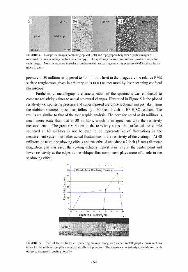
Furthermore, metallographic characterization of the specimens was conducted to compare resistivity values to actual structural changes. Illustrated in Figure 5 is the plot of resistivity vs. sputtering pressure and superimposed are cross-sectional images taken from the niobium sputtered specimens following a 90 second etch in HF-H2SO4 etchant. The results are similar to that of the topographic analysis. The porosity noted at 40 millitorr is much more acute than that at 30 millitorr, which is in agreement with the resistivity measurements. The greater variation in the resistivity across the surface of the sample sputtered at 40 millitorr is not believed to be representative of fluctuations in the measurement system but rather actual fluctuations in the resistivity of the coating. At 40 millitorr the atomic shadowing effects are exacerbated and since a 2 inch (51mm) diameter magnetron gun was used, the coating exhibits highest resistivity at the center point and lower resistivity at the edges as the oblique flux component plays more of a role in the shadowing effect.
0 5 10 15 20 25 30 35 40 450
5
10
15
20
25
30
35
40
Resistivity vs. Sputtering Pressure
Res
istiv
ity (�
�-c
m)
Sputtering Pressure (mT)
FIGURE 5. Chart of the resitivity vs. sputtering pressure along with etched metallographic cross sections taken for the niobium samples sputtered at different pressures. The changes in resistivity correlate well with observed changes in coating porosity.
(a) (b) (c)
optical heightmap
coating
substrate
1726

0 2 4 6 8 10 120
10
20
30
40
50
60
70
80
90
100
Res
istiv
ity (�
�-c
m)
Gas Impurities (% Process Gas)
Resistivity vs. Impurity Level
FIGURE 6. Chart of resistivity vs. impurity level for niobium samples deposited at varying background gas impurity levels.
TABLE 2. Average thickness and resistivity, the errors represent one standard deviation.
Sample Average Thickness (�m) Average Resistivity (��-cm)
Nb-A1 40.8� 0.7 86.9� 3.1 Nb-A2 15.9� 0.5 37.0� 1.5
Nb-1 47� 1.5 14.7� 0.5 Nb-2 58� 4 17.5� 0.7 Nb-3 35� 4 32.3� 5.8
Two specimens (Nb-A1 and Nb-A2) were deposited to test the correlation of
resistivity and coating impurity levels. As stated in the procedure, impurity level was regulated using a controlled leak and an Inficon residual gas analyzer. The results of the scans are given below in Figure 6. Overall, the resistivity scans indicate a fairly uniform value across the samples. There is a much more visible correlation between resistivity and background gas pressure than there is for the case of sputtering pressure. As expected, there is an increase in resistivity of the coatings as background gas pressure is increased. For a residual impurity level of 5% process gas, there is greater than a factor of two increase in resistivity. For 10% process gas impurity levels, there is approximately a factor of six increase. This indicates that the eddy current decay method of resistivity measurement is extremely sensitive to coating contamination levels.
SUMMARY AND CONCLUSIONS
Table 2 gives a summary of resistivity measurements acquired for the Nb samples.
1727

A dual-probe resistivity scanner based on eddy currents was designed used to determine the resistivity of niobium coatings. The results obtained from the limited sample set are in good agreement with other published measurements with other approaches. The pulsed eddy current method was used to develop a technique that allows for fast data acquisition rates with up to 105 samples per second. This fast scanning capability makes this method useful for coating diagnostics during the manufacturing process as well as in the field.
In support of the robust and reliable method developed, several correlations were made between the resistivity measurements and the coating properties. The relationship between resistivity and impurity level is quite dramatic and is easily differentiated utilizing eddy current. The resistivity of the coatings vs. sputtering pressure (e.g. density) was differentiable as measured with eddy current and the results correlated well with density changes as measured qualitatively via surface and metallographic imaging.
REFERENCES 1. Moulder, J. C., Uzal, E, and Rose, J. H., Rev. Sci. Instrum. 63 (6), 3455-3465 (1992). 2. Tai, C. C., Rose, J. H., and Moulder, J. C., Rev. Sci. Instrum. 67 (11), 3965-3972(1996). 3. Lebrun, B., Jayet, Y., Baboux, J., NDT & E International 30 (3), 163-170 (1997). 4. Clauzon, T., Thollon, F. and Nicolas, A., IEEE transactions on Magnetics, 35(3),
1873-1876 (1999). 5. Giguere, S., Lepine, B., Dubbis, J. M., Res Nondestr, 13, 119-129 (2001). 6. Danon, Y. and Lee, C., “Characterization of Ta Thin Coating Using Eddy Current
Method”, Proceedings of the ASNT spring conference, Orlando, Forida, 2003, pp. 40-41.
7. Danon, Y., Lee, C., Mulligan, C., and Vigilante, G., IEEE transaction on Magnetics 40 (4), 1826-1832, 2004.
8. Blitz, J., Electrical and Magnetic Methods of Non-Destructive Testing, Chapman & Hall, Second edition, 1997.
9. Thornton, J.A., Journal of Vacuum Science and Technology A 4 (6), 3059-3065 (1986). 10. Catania, P., Roy, R. A., and Cuomo, J. J., J. Appl. Phys. 74 (2), 1008-1014 (1993). 11. Cheng, C. C., Dodd, C. V., and Deeds, W. E., International journal of nondestructive
testing, 3, 109-130 (1971). 12. Thornton, J. A., Annual Review in Material Science, 7, 239-260 (1977). 13. Műller, K. H., J. Appl. Phys., 62, 1796-1799 (1987).
1728


![Phase stability of AlYB14 sputtered thin filmshenkelmanlab.org/pubs/kolpin09_355006.pdf · AlxYyB14 samples were synthesized by magnetron sputtering within a combinatorial setup [12]](https://img.dokumen.tips/doc/110x75/5e4bb86a8d90841bf1702312/phase-stability-of-alyb14-sputtered-thin-alxyyb14-samples-were-synthesized-by-magnetron.jpg)

![On the Deposition Rate of Magnetron Sputtered Thin … · On the Deposition Rate of Magnetron Sputtered Thin Films at ... in reference [20], it was ... generically employed to avoid](https://img.dokumen.tips/doc/110x75/5b5fcd617f8b9a7f038b9566/on-the-deposition-rate-of-magnetron-sputtered-thin-on-the-deposition-rate-of.jpg)