Embed Size (px)
Citation preview

Nonideal Conductor Models
吳瑞北
Rm. 340, Department of Electrical Engineering
E-mail: [email protected]
url: cc.ee.ntu.edu.tw/~rbwu
S. H. Hall et al., High-Speed Digital Designs, Chap.5 1
R. B. Wu
What will You Learn
• How to model lossy tx-lines?
• How to deal with tx-line loss due to finite
conductivity of metal?
• How to calculate dc and skin-effect loss?
• How to deal with tx-line loss due to
conductor surface roughness?
• How to model surface roughness loss?
2

R. B. Wu
Tx-Line Losses
• Conductor Losses
– DC losses in the conductor
– Frequency dependent conductor losses
• Lossy TEM Theory & Computations
• Surface Roughness
3

R. B. Wu
Nonideal Effects
• Driving forces by IC
– Higher speeds, with higher frequency content
– Smaller form factors, with shrinking dimensions
• High-speed impacts on design
– Some high-speed characteristics largely ignored in
designs of the past becomes critical in modern times.
– Deal with technically difficult issues
– Contend with a greater number of variables
4

R. B. Wu
Transmission Line Losses (cont’d)
• Three categories of losses
– Metal losses: normal metals not infinitely conductive
– Scattering losses: surface of metal not perfectly smooth
– Dielectric losses: Dipoles oscillating with applied time
varying field takes energy
• Effects of losses
– Degrade amplitude, severe problems for long buses
– Degrade edge rates, significant timing push-outs
– Degrade waveform, severe ISI due to dispersive loss
– Ultimately a primary speed limiter of current technology
5

R. B. Wu
Incorporate Losses Into Circuit Model
• A series resistor, R, to account for conductor
losses in both power and ground planes.
• A shunt resistor, G, to account for dielectric losses
L ∆z R ∆z
C ∆z G ∆z
6
∆z

Conductor Losses
7

R. B. Wu
DC Resistive Losses
w
t
Reference Plane
Current flows through
entire cross section of signal
conductor and ground plane
cross-section
DCRA wt
Low freq. current spreads out as much as possible.
DC losses dominated by cross sectional area & inverse of conductivity of signal conductor
DC loss by ground plane is negligible.
DC losses of FR4 are very negligible 8

R. B. Wu
Typical DC Losses
• As dimensions shrinking, losses are often a first-order effect
which degrades SI and deserves rigorous analysis.
• DC losses are of particular concern in small geometry
conductors, very long lines, and multiload buses.
W
L
tR
1dc
Ω/m 23.0
mm5.1 ,05.0
line PCBFor
mS 1058 :Ex. 6
Cu
R
Wt
Ω/mm 3.2
m515
line ICFor
R
., Wt
9

R. B. Wu
AC Resistive Losses
High-freq. current migrates towards periphery, “skin effect”.
Current flows in a smaller area than DC case. As such, the resistance will increase over DC
Outer (Ground)
conductor
Inner (signal)
conductor
Areas of high
current density
Coaxial Cable Cross Section at High Frequency
10
R. B. Wu
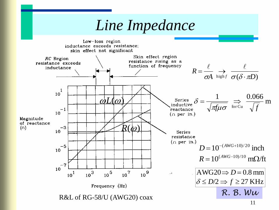
Line Impedance
)( high DAR
f
m 066.01
Cu for ff
R&L of RG-58/U (AWG20) coax
/ftm 10
inch 10 10/)10(
20/)10(
AWG
AWG
R
D
KHz 27/2
mm 8.0 AWG20
fD
D
11
( )L
( )R

R. B. Wu
Propagation Constant
f :region
effect Skin flat :region
loss-Low
f
:region RC
12
( )
j
R j L j C

R. B. Wu
Wave in Conductive Media
0y z
x 0
Conductor
(, , ) air
22
2
Propagation in x direciton:
0; =d
E jdx
good conductor
Maxwell equations:
i
E j H
H J E j E E
2
; E j H j E
E E E
2
Wave eq.:
0; j E
13

R. B. Wu
Plane Wave Field
Electric filed :
( ) x x j x
s s
E
E x E e E e e
Propagation constant :
12
j j
1 1 1Skin depth: x
xe e
f
Magnetic filed :
ˆ1 1ˆ ( )
xsE E e
H
xH x E E x E
j j Z
EWave impedance Z
H
j j
x
E
H
14

R. B. Wu
Skin Depth In Copper
0
1
2
3
4
5
6
7
8
9
10
0.E+00 1.E+09 2.E+09 3.E+09 4.E+09 5.E+09 6.E+09
Frequency, Hz
Skin
Dep
th,
mic
ron
s
Skin Effect
When field impinges upon conductor, field will penetrate conductor and be attenuated
Remember signal travels between conductors
Field amplitude decreases exponentially into a skin depth of conductor, defined as the penetration depth at a freq. where amplitude is attenuated 63% (e-1) of initial value
1
f
X Am
pli
tud
e
Penetration into conductor
Electromagnetic
Wave
15

R. B. Wu
Skin Effect – Spatial View
Fields induce currents flowing in the metal
Total area of current flow can be approximated to be in one skin depth because total area below exponential curve can be equated to area of a square
Skin Depths
0
0.1
0.2
0.3
0.4
0.5
0.6
0.7
0.8
0.9
1
0 1 2 3 4 5 6
Cu
rren
t
(1 ) /
0( , ) ( ) j zJ y z J y e
Area w
w
t
16

R. B. Wu
Calculation of Skin-Effect Resistance
Skin Depths
0
0.1
0.2
0.3
0.4
0.5
0.6
0.7
0.8
0.9
1
0 1 2 3 4 5 6
Cu
rre
nt
(1 ) /
0
(1 ) /
0 0
0 0 0
( , ) ( )
( ) ( )1
j z
w w
j z
J y z J y e
I J y dy e dz J y dyj
Area w
w
t
2 2
0 0 0 0Assume uniform current: ( ) ACJ y J R w J wJw
2 2 22 /
0 0
0 0 0 0 0
2 22
2 2
0 0 0
0 0 0
( , ) ( ) ( )2 2 4
( ) ( ) ( )2 4
w w w
z
d
w w w
AC ACd AC
P dy J y z dz J y dy e dz J y dy
R RP I J y dy R J y dy J y dy
17

R. B. Wu
Microstrip R due to Signal Conductor
Assumptions on current flow: confined to on skin depth; while return path neglected
concentrated in lower portion of conductor due to local fields
current_flow
AC
f fR
A w w w
w t E-fields
18

R. B. Wu
Resistance will stay at approximately the DC value until skin
depth is less than conductor thickness, then it will vary with
f
Example of frequency dependent resistance
0
5
10
15
20
25
30
35
40
0.E+00 1.E+09 2.E+09 3.E+09 4.E+09 5.E+09 6.E+09
Frequency, Hz
Resis
tan
ce,
Oh
ms
Microstrip Freq-Dependent R Estimates
R tot R DC R AC Frequency
R R0 Rs f
Tline parameter terms
R0 ~ resistance/unit length Rs ~ resistance/sqrt(freq)/unit length
19
Unphysical, since not
an analytic function

R. B. Wu
Microstrip R due to Return Path
Return current in reference plane also contributes
2
1( )
1 ( / )
OII y
h y h
w
t
Effective width estimated for area of return current flow.
h
y
2
02
0
( )2
ground
effective
R I y dyA hI
(Current Density in plane)
20

R. B. Wu
Total Microstrip AC Resistance
Total resistance is approximately sum of signal and ground path resistance
1 1/m
2total
FR
w h
groundsignaltotalAC RRR _
This is an excellent “back of the envelope” formula for microstrip AC resistance
21

R. B. Wu
Empirical Formula – Microstrip (by Collins)
Derived using conformal mapping techniques
Being not exact, it should only be used for estimates
2
2
0.94 0.132 0.0062 for 0.5 10
1 for 0.5
1 1 4 1ln
1 1for 0.1 10
5.8 0.03( )
signal
ground
w w w
h h h
w
h
w fR LR
t w
LR
f wR
w h h w h h
22

R. B. Wu
In stripline, fields are referenced to two planes. Total current distributes in both planes, and in both upper and lower portions of signal conductor
2 ) / ( 1
1 ) (
h y y I
For example: in symmetrical stripline, area in which current travels increases by 2 and R decreases by 2.
This inspires the parallel microstrip model
Stripline Losses
23

R. B. Wu
where the resistances are calculated from the microstrip formulae at appropriate heights.
( 1_ ) ( 2 _ )
_
( 1_ ) ( 2 _ )
h micro h micro
ac strip
h micro h micro
R RR
R R
w t
h1
h2
Calculating Stripline Losses
24
R. B. Wu
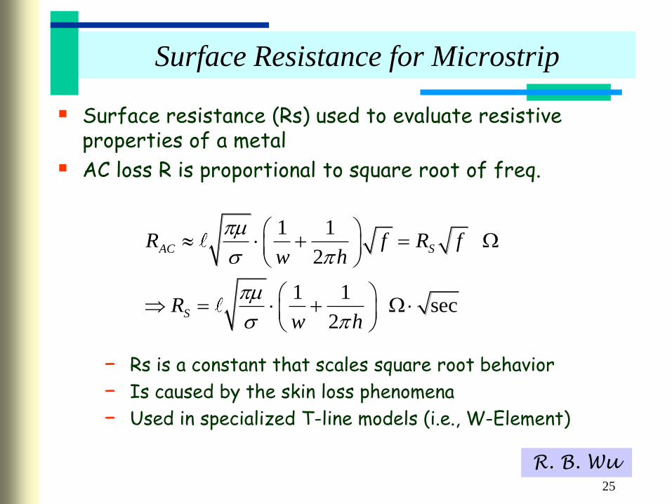
Surface Resistance for Microstrip
Surface resistance (Rs) used to evaluate resistive properties of a metal
AC loss R is proportional to square root of freq.
1 1
2
1 1sec
2
AC S
S
R f R fw h
Rw h
− Rs is a constant that scales square root behavior
− Is caused by the skin loss phenomena
− Used in specialized T-line models (i.e., W-Element)
25

Lossy TEM Theory &
Computations
26
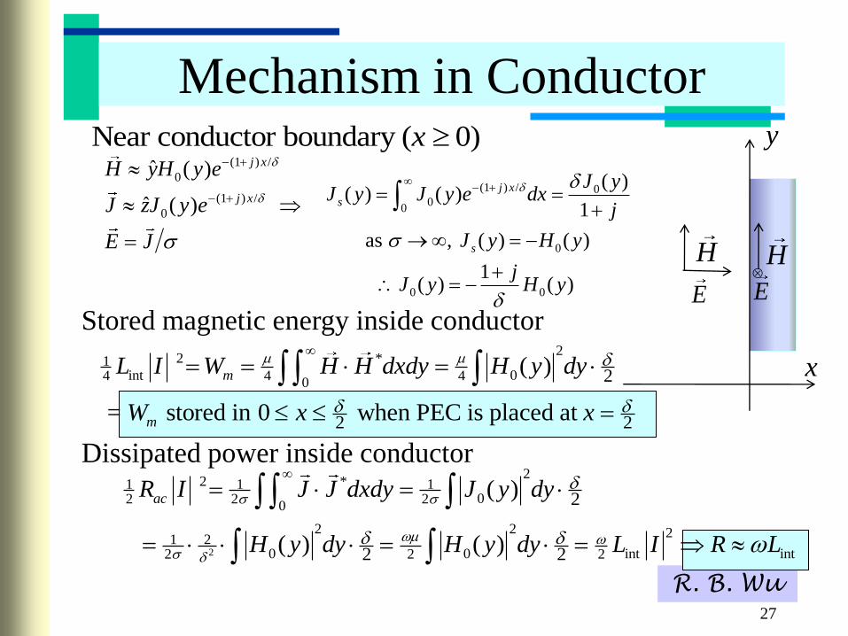
R. B. Wu
22 *1
int 04 4 40 2
2 2
( )
= stored in 0 when PEC is placed at
m
m
L I W H H dxdy H y dy
W x x
Mechanism in Conductor
x
y Near conductor boundary ( 0)x (1 ) /
0
(1 ) /
0
ˆ ( )
ˆ ( )
j x
j x
H yH y e
J zJ y e
E J
(1 ) / 00
0
0
0 0
( )( ) ( )
1
as , ( ) ( )
1( ) ( )
j x
s
s
J yJ y J y e dx
j
J y H y
jJ y H y
Stored magnetic energy inside conductor
Dissipated power inside conductor
2
22 *1 1 1
02 2 20
2 2 21 2
0 0 int int2 2 2
2
2 2
( )
( ) ( )
acR I J J dxdy J y dy
H y dy H y dy L I R L
H
27
H
E E

R. B. Wu
h2+δ
w-δ
t-δ
h1+δ
δ/2
δ/2
h2
w
t
h1
Incremental Inductance Rule (Wheeler, 1942)
• At high frequencies, say, < 0.1t, current crowds
to conductor surface within a skin depth of .
n
LLfLLL
n
L(f)RR
extext
s
2)(
2
int
28

R. B. Wu
2
1
( , )
0 0 0
ˆ
jkz
z z t z
t t z
x y e
E j A jk A
H H A z
Lossy-TEM Modal Field Theory
Ref. R. B. Wu and J. C. Yang, “Boundary integral equation formulation of skin effect problems in
multiconductor transmission lines,” IEEE Trans. Magn., vol. 25, pp. 3013-3016, July 1989.
z
Total current:
1 E
j n
zI E dA
ds
1 ˆ;
;
zH A A zA
E j A
Free space: TEM ( )z tE E
Conductor: TM/LE ( )j 2
1 1
0
0 const. in (x,y)
ˆ ˆ
t z z
t t
z z
t t z t zj
H J E E j E
E
E j A d dz
H A z E z
B.C. at : (tang. H continuous)m
mz z
z z
j A E d dz
A Ej
n n
R.C.: const. at zA
gnd
1
Parameters:
( )
m
M
mn mn n
n
d dz d dz
R j L I
29

R. B. Wu
Applications to Parallel Plates
• Solution of PDE’s:
• Matching B.C.’s:
• I-V relation:
x
y
h
w
1d dz V
2d dz V
2 0z zA j A b y
2 ( /2)0 y h
z z zE j E E a e
21
21
hz z
hz z
j A E d dz b a V Va
j A n E n b a
/2
/22
1 1
1
wz z
hw
E dE w wI ds dx a V
j n j dy j j
1 22 ( )d dz d dz V R j L I
2 22 2 (1 ) 2 (1 ) 2 2h hV j hR j L j
I w w w w w
int ext int
2; ;
RR L L L L
w
30

R. B. Wu
Parallel Plates (low-freq. limit)
• Solution of PDE’s:
• Matching B.C.’s:
• I-V relation:
x
y
h
w
1d dz V
2d dz V
2for : h
zy j A b y
2 2 2for 0 at h h h
zy d dE dy y d
2
2
cosh
sinh cosh sinh
h
h
b a d V Va
b a d d d
22 2
1 sinh
cosh sinh
z z z
hh h
y d y
E w dE dE w dI ds V
j n j dy dy j d d
2 2
tanh
V hR j L j
I w d w
2 213
intlow freq.
limit
2 2(1 ) 2 2
tanh 3
d dR j L j
w d wd wd w
d 2
cosh hzE a d y
Validate Lint by solving static magnetic field and finding stored energy? 31
tanhdc ac
j dR j L
j d
R. B. Wu
Validation of Low-Freq. Inductance
x
y
h
w
d
Hx
2 2ˆ( , ) for h h
IJ x y z y d
wd
in conductorˆ ( );
0 in free space
Iwdx
x z
H J
dHH xH y J
dy
2( - ) in conductor
in free space
hIwd
x Iw
d yH
2
2 2 32 2
2 2 20
12 2
2 2 2 3 2
h d
m x
I wh I wdW dx H dy LI
w w d
int
2
3ext
h dL L L
w w
Current flow
Magnetic field
Stored magnetic energy
32

R. B. Wu
Proximity Effect
X (cm) X (cm)
Rem: Proximity effect causes a slight increase in attenuation
( 4.7mm)
33

R. B. Wu
20.2
1
z
y
x
1 V
Example - Lossy Tx-Line
Current
distribution
unit: mm
34

R. B. Wu
Current Distribution vs. Frequency
35

R. B. Wu
Three-conductor Example
2,4,8
2,4,8
Inte
rnal
induct
ance
36

Surface Roughness
37
R. B. Wu
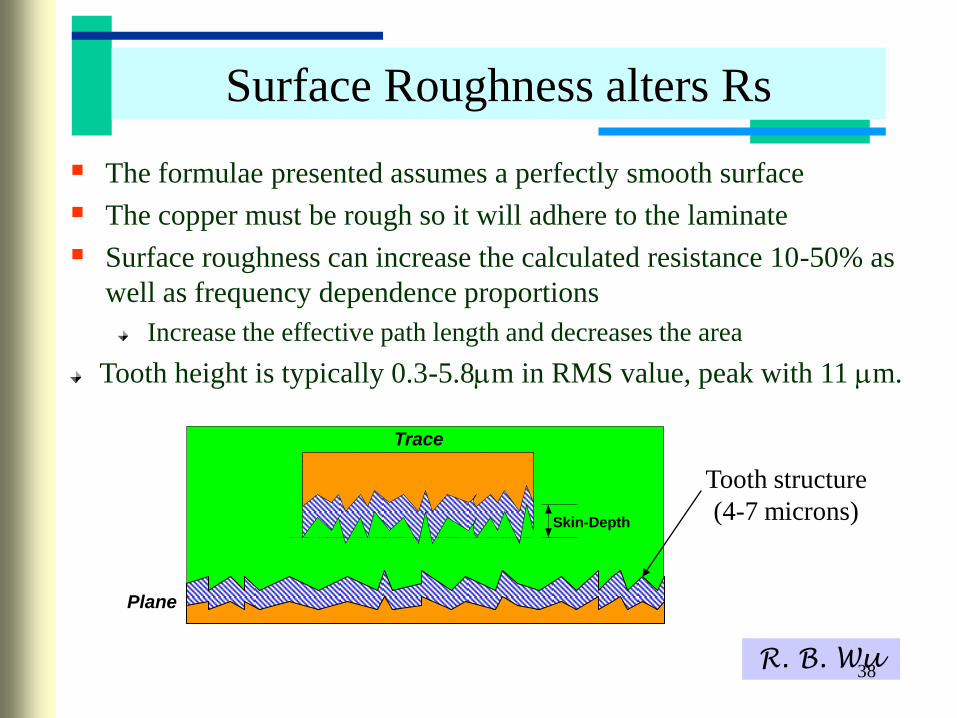
The formulae presented assumes a perfectly smooth surface
The copper must be rough so it will adhere to the laminate
Surface roughness can increase the calculated resistance 10-50% as
well as frequency dependence proportions
Increase the effective path length and decreases the area
Tooth height is typically 0.3-5.8m in RMS value, peak with 11 m.
Skin-Depth
Plane
Trace
Tooth structure
(4-7 microns)
Surface Roughness alters Rs
38

R. B. Wu
Frequency Dependence
• Surface roughness is not a significant factor until skin depth
approaches the tooth size (typically 100 MHz – 300 MHz)
• At high freq., loss becomes unpredictable from regular geometric
object because of heavy dependence on a random tooth structure.
– No longer varies with the root of freq. – something else
• Measurement
221
1
2
1
( )20log ;
( )
: received power
: injected power
P fS
P f
P
P
39

R. B. Wu
do not equal
PCB PerformancePCB Performance
PCB ModelingPCB Modeling
2 right turns a right and a left.
PCB X-sectionPOOL Stackup
FiberglassBundles
Tooth
Structure
Measurements indicate that the surface roughness may cause the AC resistance to deviate from f0.5
Example of Surface Roughness
40

R. B. Wu
hRMS
Hammerstad Model [1980]
Hammerstad coeff.:2
121 tan 1.4 1 2RMS
H
hK
Skin-effect R & L
if ( )
if
( )if
2 ( )
( )if
2
H sH
dc
H
H ext
H t
t
K R f tR f
R t
R ft
fL f L
R ft
f
;ac H sR K R f
1.2 mRMSh
5.8 mRMSh
measurement
Hammerstad
41

R. B. Wu
Surface Profile Measurement
• Hammerstad model
breaks down in case
of very rough copper
foil. Other models
needed.
42

R. B. Wu
Hemispherical Model
• The rough surface is characterized
as random protrusions.
• Assume a TEM incident on the
hemisphere at a grazing angle.
• Calculate total cross section tot of
a sphere, then divide it by two
gives power loss of hemisphere.
• Power loss absorbed by flat
conducting plane is also
considered.
1 1tot2 2 base
tile tile4
1 ;
( , )
hemi
tot
AK
A A
f kr r
43
R. B. Wu
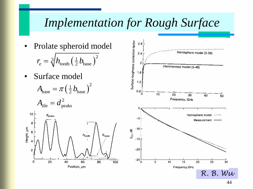
Implementation for Rough Surface
• Prolate spheroid model
• Surface model
2
13tooth base2er h b
2
1base base2
2
tile peaks
A b
A d
44

R. B. Wu
Huray Model [2009]
• N is determined s.t. total surface
area equals that of the
hemispheroid constructed before.
Fig. 5-23 1
tot21Huary
tile4
1 ;
N
nKA
1 2
base tooth
2
base
tooth
sin 1;
2 1
2
lat
b hA
b
h
lat
2; sphere radius, e.g., 0.8 m
4
AN a
a
45

R. B. Wu
Results & Comparisons
• Huray model predicts I.L.
with error < 1.5dB up to
30GHz.
• Hammerstad model saturates
at 2, not enough loss for
rough copper. It should be
used only for hRMS < 2m
• Hemisphere model over-
predicts loss at middle freq.
and slightly under-predicts at
high freq.
Fig. 5-26
46

R. B. Wu
Did You Learn
• How to incorporate loss into tx-line model?
• How conductor loss will affect propagation constant
and attenuation of tx-lines?
• How to calculate dc and skin-effect resistance for
microstrip and striplines?
• How to describe change in em-field of tx-line due to
conductor finite conductivity?
• How to model tx-line resistance due to conductor
surface roughness?
• Can you distinguish Hammerstad and Huray model?
47

R. B. Wu
Further Reading -1
• W. T. Weeks, L. L. Wu, M. F. McAllister, and A. Singh, “Resistive
and inductive skin effect in rectangular conductors,” IBM J. Res.
Develop., vol. 23, pp. 652-660, Nov. 1979.
• R. B. Wu and J. C. Yang, “Boundary integral equation formulation of
skin effect problems in multiconductor transmission lines,” IEEE
Trans. Magn., vol. 25, pp.3013-3016, July 1989.
• A. J. Gruodis and C. S. Chang, “Coupled lossy transmission line
characterization and simulation,” IBM J. Res. Develop., vol. 25, pp.
25-41, Jan. 1981.
• R. Ding, L. Tsang, and H. Braunisch, “Random rough surface effects
in interconnects studied by small perturbation theory in waveguide
model,” Proc. IEEE EPEPS, 2011, pp. 161–164.
• R. Ding, L. Tsang, and H. Braunisch, "Wave propagation in a
randomly rough parallel plate waveguide," IEEE T-MTT, May 2009.
48

R. B. Wu
Further Reading -2
• X. C. Guo, et al., "An analysis of conductor surface roughness effects
on signal propagation for stripline interconnects,“ T-EMC, pp. 707-
714, Jun. 2014.
• B. Curran, et al., "On the modeling, characterization, and analysis of
the current distribution in PCB transmission lines with surface
finishes,“ T-MTT, pp. 2511-2518, Aug. 2016.
• M. Y. Koledintseva, et al., "Method of effective roughness dielectric in
a PCB: measurement and full-wave simulation verification,“ T-EMC,
pp. 807-814, Aug. 2015.
• F. Bertazzi, et al., "Modeling the conductor losses of thick multi-
conductor coplanar waveguides and striplines: A conformal mapping
approach," T-MTT, pp. 1217-1227, April 2016.
• A. V. Rakov, et al., "Quantification of conductor surface roughness
profiles in printed circuit boards," T-EMC, pp. 264-273, Apr. 2015.
49