Embed Size (px)
Citation preview
NATIONAL RADIO ASTRONOMY OBSERVATORY
CHARLOTTESVILLE, VIRGINIA
ELECTRONICS DIVISION INTERNAL REPORT NO. 286
DESIGN AND PERFORMANCE OF CRYOGENICALLY-COOLABLE,
ULTRA LOW-NOISE, L-BAND AMPLIFIER
J. D. GALLEGO AND M. W. POSPIESZALSKI
MARCH 1990
NUMBER OF COPIES: 150

DESIGN AND PERFORMANCE OF CRYOGENICALLY-COOLABLE, ULTRA LOW-NOISE, L-BAND AMPLIFIER
J. D. Gallego and M. W. Pospieszalski
Table of Contents
1. Introduction 1
2. General Design Considerations 2
2.1 Model of Signal and Noise Properties of FHR02X M0DFET 2
2.2 Amplifier Design Trade-Offs 4
3. Characterization of Passive Circuits 8
3.1 Microstrip on Duroid Substrate at Room and Cryogenic Temperatures 8
3.2 Characterization of Lumped Elements 11
4. Noise Temperature Measurement of Cryogenically-Coolable Amplifiers . 11
4.1 Noise Measurement System 11
4.2 Accuracy Considerations 15
5. 1.2-1.8 GHz, Three-Stage Amplifier with Optimal Noise Performance at Cryogenic Temperatures 15
5.1 Electrical Design 15
5.2 Realization 18
5.3 Comparison Between Measured and Predicted Results 21
6. Discussion and Conclusions 25
References 26

DESIGN AND PERFORMANCE OF CRYOGENICALLY-COOLABLE, ULTRA LOW-NOISE, L-BAND AMPLIFIER
J. D. Gallego and M. W. Pospieszalski
1. Introduction
This report presents the design and performance of a cryogenically- coolable, 1.2-1.8 GHz amplifier. This design supersedes the very successful and widely copied previous NRAO design for the same frequency band [1], [2]. It differs, however, from the previous design in several important aspects, both in the design approach and realization. Recent advances in the understanding of noise properties of cryogenic FET's [6], [7] allowed for the computer-aided design [4], [6] of a nearly "optimal" amplifier from the point of view of the following criteria:
• lowest possible average noise temperature across the band of interest.
• high gain (> 35 dB) with as small gain variation as possible.
• low input and output reflection coefficients.
• unconditional stability at any physical temperature in the range 4 K < Te < 300 K.
This design was implemented in hybrid MIC technology. Commercially- available HEMT chips from Fujitsu (FHR02X) and Mitsubishi (MGFC4404) were used. Matching and coupling networks were realized in microstrip form. Only one tunable element, a coil, was allowed in the design.
Very careful characterization of distributed and lumped components used in the design and also Monte Carlo analysis of measurement errors [19] allowed for a meaningful comparison of measured results with those predicted from the wideband noise model of a MODFET [6], [7]. The measured performance of amplifiers, both at room and cryogenic temperatures, is within the measurement error from those predicted by the amplifier model.
Section 2 of this paper contains a discussion of the signal and noise properties of FHR02X MODFET's and amplifier design trade-offs. Section 3 is devoted to characterization of passive circuits used in amplifier realization. Measurement setup and its accuracy are discussed in Section 4. A detailed description of the design and realization of the amplifier, as well as the comparison between measured and predicted results, is presented in Section 5. Finally, a discussion of the results and brief conclusions are offered in Section 6.
2. General Design Considerations
2.1 Model of Signal and Noise Properties of FHR02X MODFET
The model for the FHR02 device, both in packaged and chip form, was developed in precisely the same way as described in previous papers [6], [7] for other devices. A single frequency noise parameters measurement and small signal equivalent circuit, as shown in Figure 1, were used to determine the equivalent temperatures of intrinsic gate resistance and drain conductance, Tg and Td [6], [7], A comparison between model prediction and measured results for the FHR02FH (packaged) device at 8.5 GHz is summarized in Table I. The best-fit values of Tg and T^ at room temperature (297 K and 1783 K, respectively) and at a temperature of 12.5 K (16.3 K and 523 K, respectively) were used to predict the noise performance in the frequency range of interest. The results for the FHR02X device are shown in Table II for ambient temperatures of 297 K and 12.5 K.
.004
G o-
J2
.42 -nnr*-
r .026 71
.16:
^NAA-
H4 4.5 > Tg
9„e~JWZvn Td >197
-A/V^
.047
L CHIP .5
gM= 52.4 nS
Z_2_2 ps ,
.072
.42
.16
-o I
:.08
"^\^ @ 12.5 K @ 297 K
Td 523 1783
Tg 16.3 297
Fig. 1. Equivalent circuit of FHR02FH (packaged version) and FHR02X (chip version). Chip elements are enclosed by the dotted line. Values are Q, nH and pF.

TABLE I. Noise Parameters of FHR02FH MODFET at 8.5 GHz
MEAS. COND.
COMMENTS T . mm
K
R opt
Q
X opt
Q
gn
mS
T g K
Td
K
Ta-297 K
Vds«2 V
Ids-10 mA
Measured 51.0 10.7 26.3 5.7 - -
Model Best Fit 48.5 11.4 27.7 6.9 297 1783
Ta-12.5 K
Vds-2 V
Ids-5 mA
Measured 7.3 5.3 26.3 1.70 - -
Table II. Noise Parameters of FHR02X MODFET at Ta - 297 K and T. - 12.5 K
Noise Parameters (T - 12.5 K)
Freq. Tmin Ropt Xopt gn
1.00 .71 195 740 .0062 1.20 .86 162 615 .0089 1.40 1.00 139 526 .0121 1.60 1.15 122 459 .0157 1.80 1.30 108 407 .0199 2.00 1.45 97 365 .0246
Noif se Parameters < [T - 291 1 K)
Freq. Tmin Ropt Xopt gn
1.00 5.6 458 769 .0212 1.20 6.8 382 640 .0305 1.40 7.9 327 547 .0415 1.60 9.1 286 478 .0542 1.80 10.2 255 423 .0686
The circuit shown in Figure 1 is for the packaged version FHR02FH, and only the elements enclosed by dotted lines represent the chip. When a chip model is used, the inductance of the bonding wires should be included, but not the additional elements associated with the package. The exact value of the bonding wire inductances is not critical for L-band modeling. For the noise parameter data of Table II, values of .4 nH in gate and drain and .08 nH in source were used.
All the dissipative elements in the equivalent circuit in Figure 1 generate pure white noise. The noise generated in the parasitic resistances of gate, drain and source is determined by the ambient temperature, while the noise generated in the intrinsic gate and drain resistors is determined by their equivalent temperatures, Tg and Td, respectively. Noise in both resistors is completely uncorrelated. The equivalent circuit in Figure 1 does not represent 1/f or G-R noise, which contribution in cryogenic L-band amplifiers has been suggested in the past [1]. Nevertheless, this model allows the prediction of amplifier performance within experimental error of measured values.
It should be stressed that the equivalent circuit of Fig. 1 was developed from wideband S-parameter data for FHR02 MODFET, in both the packaged version (1-16 GHz) and chip version (1-26 GHz), for the bias of Vds - 2 V and Ids - 10 mA [20] . The validity of this model is also assumed for a cryogenic device for the bias of Vds - 2 V, Ids - 5 mA. Although this assumption was never directly confirmed by cryogenic measurements of the S-parameter data, it is justified by the observation that values of g,,^ and rds, the only two elements of equivalent circuit strongly dependent on temperature, are for Ids - 5 mA and Ta - 12.5 K about the same, as they are for Ids - 10 mA at Ta - 297 K, according to dc measurements.
2.2 Amplifier Design Trade-Offs
The circuit model of Figure 1 can be used to calculate noise and S-parameters of the FHR02X transistor in L-band. The results for ambient temperature of 12.5 K for L-band are shown in Table III and Figure 2. The loci of values of both S^ and ropfc are very close to the edge of the Smith chart, underscoring the fact that, for L-band frequencies, the direct measurement of noise parameters might not necessarily yield more accurate results than those predicted from the model. The noise temperature of an amplifier for some generator impedance Zg - Rg + j Xg can be expressed in terms of the parameters of Table III as:
T - T . + T -^- [(R - R J2 + (X - X J2] (1) n mm o R g opt g opt J '
where T0 is the standard temperature (290 K). The stability factor K is defined as:

K 11 22 Sll S22 ' S12 S21 S12 S21
(2)
For an unconditionally stable device, K > 1. For K < 1, the transistor is prone to oscillations for certain values of generator and load impedance if special precautions are not taken. The addition of any lossless input or output matching network does not change the value of the stability factor and other means, like lossless feedback or dissipative loading, should be employed.
.5 ..••" •-, 2
2 /.
0
Ropt
£ 10 .2 I '12:::::
■■...■■■^S2^
■;V$*MH
- . 2\ .'■:■?'-5 51 1
S- •'-2
-1
Fig. 2. Smith chart plot of Sllt S22 and ropt for FHR02X transistor at ambient temperature Ta - 12.5 K.
Table III. Signal and Noise Parameters of FHR02X in L-Band at Ta = 12.5 K. The Units for Noise Parameters are K, 0, and mS.
11 12 21 1 22 K FREQ MAG ANG MAG ANG MAG AN6 MAG ANG FACT 1.000 .9960 -9.6 .0133 84.9 4.0654 171.0 .6035 -4.1 .08 1,Z00 .9943 -11.5 .0159 83.9 4.0637 169.2 .6025 -4.9 .09 1.400 .9923 -13.5 .0186 82.9 4.0616 167.4 .6013 -5,7 .11 1.600 .9899 -15.4 .0212 81.9 4.0592 165.6 .5999 -6.6 .12
1.800 .987Z -17.3 .0238 80.9 4.0565 163.8 .5984 -7.4 .14
NOISE PERFORMANCE PARAMETERS IXIMUM- GAIN WAS REQUESTED, WHICH DEPENDS ON: [SI
FREO e<dB> In Twin Ropt XQPt 5n Es &> 1.000 24.86 21,02 .71 195.22 740.43 .01 50.00 0.00
1.200 24.07 21.00 .86 162.71 615.94 .01 50.00 0.00
1.400 23.40 20.96 1.00 139.50 526.85 .01 50.00 0.00 1.600 22.82 * 20.93 1.15 122.10 459.89 .02 50.00 0.00 1.800 22.31 20.89 1.30 108.56 407.67 .02 50.00 0.00
For instance, S-parame-ters in Table III show that the transistor loaded with 50 ft is stable, but tiie generator impedance required to obtain power match at the input (approximately 14 + j 340 ft in the middle of the band) differs notably from "the impedance needed to obtain minimum noise. The addition of a small source inductance improves the stability in the band and increases the real part of the input impedance, making it easier to obtain simultaneously low noise and low input reflection. The drawbacks are that some gain is lost and the stability deteriorates at frequencies above the L-band. A combination of inductive feedback in the source and wideband resistive loading in the drain was found to be a good combination for unconditional stability in and out of the band. For example, if the value of the loading resistor is 50 ft and the series source inductor is 0.5 nH, good input and output match is obtained when the transistor is matched for minimum noise. A small increase in noise is expected, due to the thermal noise added by the resistor, as well as some reduction in gain. This noise increase is only about 0.25 K for a single-stage amplifier. The noise parameters and S-parameters for the transistor with feedback and resistive loading are shown in Table IV and Figure 3. The effect of these modifications is well illustrated by data in Figures 2 and 3; for the MODFET with feedback and loading, S22 is much closer to the center of a Smith chart and S^* and ropt are quite similar.
5 ..■■•-
2 ..•:
:0 :.2 i.5 '"■I i*2: : : Mr"": .V.V."
-.2V"" \ v" v. / ""'-S?-5
-.3 ••... ■••: "'".-••"-2
-1
Fig. 3. Smith chart plot of S^, S^ and ropt for FHR02X at Ta - 12.5 K with source feedback and resistive loading. Note the proximity of ropt
and Sj^*.
Table IV. Signal and Noise Parameters of FHR02X with .5 nH Inductance in Series with Source and 50 ft Resistor Loading at the Output at Ta - 12.5 K.
I S3 PflRflHETERS IN tlflGNITUOE AND PHASE
11 12 21 22 K FREQ MAG ANG MAG ANG MAG ANG MAG ANG FACT 1.000 .9776 -8.5 .0075 89.7 2.2128 160.0 .1128-156.9 1.25 1.200 .9689 -10.1 .0091 90.8 2.1850 157.5 .1093 -162.7 1.48 1.400 .9589 -11.6 .0107 91.7 2.1560 154.8 .1068 -167.3 1.70 1.600 .9479 -13.1 .0123 92.5 2.1253 152.1 .1050 -171.1 1.89 1.800 .9361 -14.5 .0140 93.1 2.0930 149.4 .1035-174.3 2.08 2.000 .9236 -15.9 .0157 93.6 2.0592 146.8 .1022 -177.0 2.24
NOISE PERFORMANCE PARAMETERS MAXI11UM-GAIN WAS REQUESTED, WHICH DEPENDS ON: [SI
FREQ G(dB) In Tmin Root Xopt Gn Rs Xs 1.000 21.64 22.87 .79 189.69 739.00 .01 50.00 0.00 1.Z00 19.69 22.82 .97 159.25 614.05 .01 50.00 0.00 1.400 18.18 22.76 1.16 137.70 524.53 .01 50.00 0.00 1.600 16.93 22.69 1.35 121.70 457.14 .02 50.00 0.00 1.800 15.85 22.60 1.55 109.39 404.51 .02 50.00 0.00 2,000 14.90 22.51 1.76 99.66 36Z.21 .03 50.00 0.00
3. Characterization of Passive Circuits
3.1 Microstrip on Duroid Substrate at Room and Cryogenic Temperatures
The role of the input matching network is to transform 50 ft impedance to the values as close as possible to the optimal source impedances over the 1.2 GHz-1.8 GHz frequency band with as little loss as possible. It also provides gate bias and plays an additional role in assuring out-of-band stability of the amplifier. These functions necessitate the use of high characteristic impedance lines which losses could greatly affect the amplifier performance. The choice of the substrate is, therefore, determined by a compromise between losses, circuit size and etching tolerances. As a result, Duroid 6010.5, .050"-thick substrate [9] was chosen for the amplifier realization. The substrate was tested for changes in dielectric constant and losses at cryogenic temperatures using a microstrip A/2 resonator with small capacitive coupling to input and output lines (Figure 4). Theoretical information on microstrip gap capacitance can be found in [11]. Typical resonance curves at room and cryogenic temperatures are shown in Figure 5. A decrease in the resonant frequency and an increase in resonator Q are observed upon cooling.
Using the HP8510 network analyzer and a data acquisition software [12], S-parameters of resonator were taken at several temperatures and the elements of the equivalent circuit shown in Figure 1 were optimized to fit the measured ^xl values. The value of the dielectric constant of the substrate can be deduced from the value of the effective dielectric constant obtained with the optimization and the microstrip model [10]. Results of these computations are shown in Figure 6. Notice that the value obtained for losses at the room temperature (L - 0.038 dB/in) is twice the theoretical value for copper lines on this substrate [10], [13], [14]. This discrepancy can be most likely explained by the influence of the surface roughness and also of the gold-plating, which was comparable in thickness to skin-depth.
Z0= 50 Dhn
L = X/2 e 1.5 GHz
C C o f- o o o
Fig. 4. Resonator used to test dielectric constant and loss at cryogenic temperatures. Line impedance in 50 ft and gap capacitance C - .035 pF.
8
t~ '5/'
vO
I I
MARk'ER 1. 46
S21 log MAG REF -50.0 dB X 10.0 dB/ V -22.561 dB
Ghz
• —
... ..^
■-
1
START 1.000000000 GHz STOP 2.000000000 GHz
(A)
S21 log MAG REF -50.0 dB ^ 10.0 dB/ V -13.566 dB T ... , . ..
START 1.000000000 GHz STOP 2.000000000 GHz
(B)
Fig. 5. Resonance curves of Duroid microstrip resonator at different ambient temperatures A) Ta - 297 K; B) Ta - 12.5 K.
X u c n \ m ■D
040
030
020 -
010
000
. *.
LINE LOSSES
i i i i i i i i i i i i
*.•••
\ ■ ■ ■ ' i ■
..•*"
■ * * ■ ■ * ■ * ■ * ■ * * ■ • ■ ■ * ■ • ■ ■ * ■ ■ ■ ■
0 50 100 150 200 250 300
Temp CK3
(A)
DIELECTRIC CONSTRNT
12.0
11.5
w 11.0 Ld
• ■»--...*
10.5
10.0
\ f I » I I I ' ' 1 I I I I I I I I I I I I I I I I I I
'"•*.
*-..
•.*
1 ■ ■ ■ ' ' • ' ■ ■ ' ' ■ ' ' ' • ■ ■ ' ' ■ ■ ■ ■
Fig. 6.
(B)
0 50 100 150 200 250 300
Temp CK]
A) Losses for the 50 ft line on Duroid 6010.5 substrate vs. ambient temperature. B) Effective dielectric constant of Duroid 6010.5 vs. ambient temperature.
10
3.2 Characterization of Lumped Elements
Coil: Computer modeling of a number of possible topologies of an input network satisfying a condition of low noise over the 1.2 to 1.8 GHz band led to the conclusion that a coil of about 50 nH, as close to an ideal as possible, should be placed in series with the input transistor gate. Any distributed realization of this series inductance caused the deterioration of noise performance over the bandwidth of interest.
A very small diameter (.040") coil was designed according to the general design rules given in [17]. The diameter was chosen to keep the self-resonance frequency sufficiently high (> 2 GHz) , yet to maintain as high a Q-factor as possible. Tests were performed on coils inserted between 50 ft microstrip lines to check for the absences of resonances in the 1-2 GHz band.
The Q-factor of a coil is expected to increase upon cooling. Tests performed on a coil model, 10 times the size of a real coil, at a frequency 10 times smaller, revealed an increase of the Q-factor by about 2 upon cooling from 297 K to 77 K.
Capacitors: Capacitors used in the amplifier design were used only as d.c. block and bypass elements. Whenever loss was considered to be of critical importance, ATC (American Technical Ceramics, [21]) #100A capacitors were used. In less critical applications, ATC //111 capacitors were employed. All capacitors were modeled as series R-L-C networks in order to include losses and self-resonance effects. Appropriate data were taken from manufacturer's catalog [21]. Losses are believed to decrease at cryogenic temperatures, but this effect was not included in modeling due to the lack of data and its relatively small Influence on amplifier performance.
4. Noise Temperature Measurement of Cryogenically-Coolable Amplifiers
4.1 Noise Measurement System
Conventional noise measurement techniques used for room temperature, low-noise amplifiers are not adequate for cryogenic amplifiers. For example, the noise figure of the amplifier described in this paper is 0.045 dB (3 K), and a typical accuracy of modern commercial noise figure meters using diode noise sources is not better than 0.1 dB [15].
by: The accuracy of noise temperature determination may be improved
• improving the accuracy with which the equivalent temperatures of "cold" and "hot" loads are known,
• decreasing the "cold" load equivalent temperature,
11
• increasing the "hot" load equivalent temperature but keeping it well within the linear range of the receiver and detector,
• reducing the change of impedance between "hot" and "cold" loads,
• and reducing the noise temperature of a receiver and the contribution of a receiver to an overall system noise temperature.
In our measurement system, the first four conditions were satisfied by using a combination of room temperature diode noise source and a cooled, 20 dB attenuator. This method of measurement, known as "cold attenuator method," has been used at NRAO since the late 1970's [22]. The "hot" and "cold" temperatures of this "composite" noise source were about 110 K and 15.5 K, respectively. The attenuator temperature was monitored by a cryogenic sensor with typical accuracy of ± 0.5 K. The ENR of the noise source with attenuator was calibrated at room temperature by comparing it with 77 K and 297 K standard loads. The change in attenuation of a stainless-steel lines and 20 dB pad upon cooling was measured and the calibration was corrected for this effect. The 20 dB pad (Narda 4779) was remarkably good at cryogenic temperature (Figure 8 and Table V). For room temperature measurements, the same diode noise source (HP-346B, Hewlett- Packard) with the 15 dB attenuator was used. "Hot" and "cold" temperatures were about 635 K and 297 K, respectively.
897 K
HP-346-B NOISE SOURCE
FROM APPLE X — COMPUTER #
ENR.-1S.2 dB
60 K
12.5 K
NARDA 477»-80
VWW
COLD ATT. (SO <ffl>
D.U.T
NRAO RECEIVER
tn TO ■*» APPLE X
COMPUTER
Tn < 500 K IRL > 80 dB
Fig. 7. A schematic of a noise measurement setup at cryogenic temperatures
12

INPUT LINE
m T3
a: en >
i- H
030
020 -
010 -
.000 0.5
i i i ■i i i i i
-* •-
* ■ *
(A)
1.0 1.5
Freq. (MHz)
2.0 2.5
070
060
INPUT LINE + 20 dB RTT.
m .050
.040
CE >
.030
•
CE
.020
000
I I I I I I I I
0.5
/
1.0 1.5
Freq. (MHz)
2.0
(B)
2.5
Fig. 8. A) Change in attenuation upon cooling of stainless-steel, coaxial dewar transition line vs. frequency. B) Change in attenuation upon cooling of dewar transition line and 20 dB attenuator vs. frequency.
13

Table V. Change in Attenuation Upon Cooling of Dewar Transition Line and Dewar Transition Line 20 dB Attenuator Cascade vs. Frequency.
VARIATION IN LOSSES FOR OEUAR LINES AND Z® dB ATTENUATOR **♦(USING TRANSDUCER 6AIN)«*» ♦•*( PORTS 1 & Z CHANGED >»** Lt. Ltc : LINE LOSSES i T»3TO & 15 K Lat, Late : ATTENUATION « T-300 & 15 K
File: DABLEI Header: COOPER LINE 1 A T-300 K
File: LINES1 Header: LINES1 A T-300 K
File: LINES1C Header: LINES1 A T-15 K
File: CABLEZ Header: COOPER LINE Z fl T-300 K
File: LINESZ Header: LINESZ A T-300 K
File: LINESZC Header: LINESZ A T-15 K
Fmin« .5 Fnaxa Z.5 Step- .05
FREQ Lt (dB) Ltc <dB> Var (dB) ■ Lat (db) Latc(dB) Var (dB)
.500 .056 .043 .01Z ■ 19.877 13.874 .003
.550 .058 .046 .012 « 13.883 19.878 .005
.600 .063 .048 .014 > 19.890 19.888 .002
.650 .064 .05Z .013 ■ 19.895 13.895 .001
.700 .069 .055 .013 ■ i 19.908 13.303 .005
.750 .070 .056 .015 ■ > 19.913 19.906 .006
.800 .077 .061 .015 ■ » 19.9Z1 13.313 .008
.850 .078 .063 .015 ■ i 19.9Z8 13.311 .018
.300 .080 .064 .016 • • 19.933 19.915 .018
.350 .081 .066 .016 ■ • 19.944 19.930 .014
U000 .083 .063 .014 • < 19.959 19.94Z .016
1.050 .086 .070 .017 i » 19.974 19.348 .026
1.100 .088 .073 .015 < ■ 19.983 13.955 .0Z9
1.150 .091 .076 .016 i • 19.988 13.358 .030
I.Z00 .035 .077 .018 ' > 19.936 13.360 .036
1.Z50 .096 .078 .018 • i 13.336 13.355 .041
1.300 .036 .081 .015 • i Z0.013 13.367 .047
1.350 .100 .085 .015 • • 20.019 13.37Z .047
1.400 .104 .086 .013 « • Z0.0Z7 19.978 .048
1.450 .103 .085 .019 • • 20.033 13.384 .055
1.500 .106 .087 .013 • i Z0.04Z 19.986 .056
1.550 .103 .083 .0Z0 i • Z0.048 19.393 .054
1.B00 .113 .034 .019 ' • Z0.053 13.997 .056
1.650 .116 .037 .019 « • Z0.059 19.997 .06Z
1.700 .1Z0 .104 .016 « ■ Z0.067 Z0.00Z .065
1.750 .1Z4 .10Z .0Z1 ■ • Z0.064 Z0.002 .063
1.800 .1Z4 .104 .0Z0 ■ • Z0.074 Z0.016 .058
1.850 .1Z5 .104 .0Z1 « ■ Z0.080 Z0.030 .050
1.300 .123 .10Z .0Z1 ■ Z0.089 Z0.043 .047
1.350 .1Z4 .103 .0Z1 ■ 20.090 20.05Z .038
Z.000 .130 .107 .0Z3 ■ Z0.079 20.055 .0Z4
Z.050 .133 .110 .0ZZ • Z0.08Z Z0.053 .0Z9
2.100 .133 .116 .0Z4 ■ 20.074 Z0.043 .031
Z.150 .14Z .117 .0Z5 ■ Z0.07G Z0.041 .035
Z.200 .141 .116 .0Z5 ■ Z0.069 Z0.041 .0Z8
Z.Z50 .14Z .119 .0Z4 ■ Z0.073 20.045 .0Z8
Z.300 .137 .114 .0Z3 ■ Z0.078 20.055 .0ZZ
Z.350 .143 .117 .026 ■ Z0.073 Z0.05S .017
Z.400 .146 .1Z0 .0Z6 ■ Z0.077 20.056 .021 Z.4B0 . 14G .118 .028 ■ 20.071 20.055 .017
14

4.2 Accuracy Considerations
A Monte Carlo method was developed for an estimation of the accuracy of the noise measurement systems [19]. The results for the system described in Section 4.1 are shown in Figure 9. The dependence of the total error (at 3 a) of noise temperature measurement is presented in Figure 9(a) as a function of amplifier gain and in Figure 9(b) as a function of amplifier noise temperature. For the amplifier with the gain of 30 dB or more and noise temperature about 3 K, the total error is about ± .9 K. This accuracy is almost independent of the input return loss of a device under test, even for highly reflective devices (IRL ~ 0 dB) . The limits of accuracy in this system are determined by the accuracy with which the attenuator cold temperature is known (± .5 K) and the accuracy of the ENR calibration of the noise source-cold attenuator combination.
The repeatability of the measurement system is better than .1 K. This makes the system ideal for optimization of amplifier noise and comparison between different devices.
Some of the noise temperature measurements were done in a liquid He dewar at the amplifier ambient temperature of 4.2 K [23]. The measurement setup is schematically shown in Figure 10. Two different loads, at 4.2 K and 18 K, were used as "cold" and "hot" loads, respectively. The 4.2 K temperature was well known (LHe boiling point) and the 18 K was measured with accuracy better than 0.5 K (Figure 7). The MC modeling of the accuracy of this system revealed it to be strongly dependent on the amplifier IRL. The estimated error as a function of the input reflection of an amplifier with Tn - 3 K is shown in Figure 11. The return loss of both "hot" and "cold" cryogenic loads is assumed to be 20 dB.
The cryogenic measurement setup of Figure 10 is more accurate than that of Figure 8 only for the amplifiers with very low input reflection coefficients.
5. 1.2-1.8 GHz, Three-Stage Amplifier with Optimal Noise Performance at Cryogenic Temperatures
5.1 Electrical Design
A three-stage amplifier was designed in accordance with the general design comments presented in Section 2. Only the input matching network was optimized for minimum noise as the gain of the first stage was sufficiently high (- 12 dB) . The interstage networks were designed for flat and highest possible gain. Without sacrifice of performance, the second and third stages were made identical. The source inductance in each of the stages is about .5 nH (compare Section 2.2). The schematic of the amplifier is shown in Figure 12. The values of the components are given in Appendix I.
15

ERROR (0 3 SIGMR)
Q: o a: u
T3
20
15
10
0
T—i—i r. | i i i i | i i i i | i t i i | i i i
3.0
2 5
m V I_J 2 .0
a: o a: 1 .5 Q: u -p 1 0 D
"D
' I ' ' ■ ' I
' + + +• 1 • ■ ■ • ' ■ ■ ■ • ' ■ ■ ' * '
•+ + I .... I
ERROR (0 3 SIGMA)
0 5 10 15 20 25 30 35 40
Gain CdB]
0.0
1- f-J-yr- T-l", V f ■I I ,1 1 i r -pi-1- ■ ■ 1 ' ■ ■1 T ,-! T ■i-r-p
■
+ ■ - ...•'"
• ....+••" .. ■•*"
•" + ■
" ..-•*"" , .+••••• ••" + : - +....• "*" - fc"
.
■
■
0 5 10 15 20 25 30 35 40
T dut CK]
(A)
(B)
Fig. 9. Accuracy of noise temperature as a function of (a) amplifier gain and (b) amplifier noise temperature.
16

297 K
77 K
4.2 K
HEATO
RECEIVER
TO — POWER
METER
Fig. 10. Noise temperature measuring system for the ambient temperature of 4.2 K.
01 O a: a: u +> D
ERROR (0 3 SIGMR)
5.0
4.0 -
3.0
2.0
1.0
0.0
j i i j i i i i i i i i i i i i i i i i i i i i i i i ' i i
•+•• •—•+...
» ■ ■ i
-+ + + 1 ■ « ■ • * • • • ■ * • ■ * ■ * * * ■ ■ ' » * ■ * *
0 5 10 15 20 25 30 35 40
D.U.T. IRL CdBI
Fig. 11. Accuracy of 4.2 K measurement system as a function of an amplifier input return loss. The amplifier noise of 3 K and the input return loss of 20 dB for both "hot" (16 K) and "cold" cryogenic loads are assumed.
17
The design of a prototype version did not take into account the presence of parasitic capacitance Cp (Figure 12). As a result, the prototype amplifier exhibited a "hump" in the noise characteristic of around .6 K in the middle of the band. The value of capacitance Cp - .2 pF was found to explain this effect. This capacitance represents the fringe effects associated with the end of the coil. In order to compensate for this effect, the characteristic impedance of the transmission line T1 was changed from 76 Q in the prototype version to 65 0 in the final version of the amplifier. Similarly, the inductance of Lj was changed from about 50 nH to 25 nH for the same reason.
The gate bias network is designed to introduce the smallest possible losses in the band and yet provide stability in the amplifier at frequencies below 1 GHz. It uses a short-circuited tuning stub as the capacitors C8 through Cg are self-resonant in the band center. The drain bias circuit uses a 50 Q loading resistor, which presence is required to assure the unconditional stability of the amplifier in and out of band.
5.2 Realization
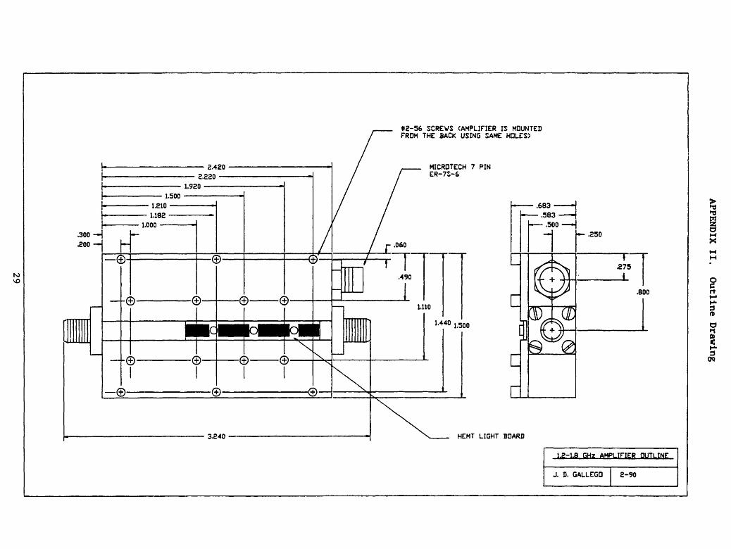
The photograph of the assembled amplifier with the cover plate removed is shown in Figure 13 and a detail of the first stage is shown in Figure 14. The milled brass chassis is electroplated with 350 pinches of "soft" gold to facilitate the bonding of MODFET chips and to protect against corrosion. Substrates are soldered to the chassis with SN62 solder. The silver-based epoxy was also used for this purpose, but the strength of the bond was insufficient for cryogenic cooling. The coil is made of #36 enameled wire, wound on an .040"-diameter drill. It is soldered to the microstrip line and to the small pad using the gap-welder (Figure 14). The input substrate has a slot cut under the coil to relieve the stress produced by substrate shrinking at cryogenic temperatures. In the absence of this slot, "the cooling of the amplifier quite often caused the gate bond wires of the first stage to break.
FET and capacitor chips Are attached with silver-based conductive epoxy (Epotek H20E, Epoxy Technology, Inc.) cured at 120oC. The source inductance in the first stage is realized with two .0007"-diameter bonding wires, .060" long at each side of the chip. The source inductance in subsequent stages is realized with four bond wires of the same length (two each side).
The cavity accommodating microstrip substrates is of sufficiently large dimensions to allow for propagation of the waveguide modes. Two sheets of the microwave absorber (MF-124, Emerson & Cumings) are attached to the walls of the cavity with Armstrong A-12 epoxy to prevent the possibility of oscillation caused by the input-output coupling via waveguide modes.
18

vo
Z (ohm) L (inches) AIR
T2 see text 1.996
76 2.007
76 1.444 76 1.406
T5 76 1.444
Fig. 12. Schematic of three-stage, L-band amplifier.
Fig. 13. A photograph of the 1.2-1.8 GHz amplifier with the cover plate removed.
Fig. 14. An expanded view of the first stage showing MODFET chip, input gate coil and drain loading and bias resistors.
20
The amplifier was designed for Fujitsu FHX04X/FHR02X MODFET chips. Experiments revealed the MGFC4404 chips from Mitsubishi can be substituted for Fujitsu chips without any deterioration in noise performance and actually some improvement in both gain and input return loss. Table VI presents the optimal bias for room at cryogenic temperature^ for FHR02X and MGFC4404 MODFET's.
TABLE VI. Optimum Bias
FHR02X MGFC4404
297 K 12.5 K 297 K 12.5 K
Vd (V) 3 3 3 3
The components list is given in Appendix I.
5.3 Comparison Between Measured and Predicted Results
The measured and modeled data for amplifier ambient temperatures of 297 K, 12.5 K and 4.2 K are shown in Figures 15, 16 and 17, respectively. At T^ - 4.2 K noise measurement system of Figure 10 was used {23]. Very close agreement between the measured and predicted noise performance is observed. The measured performance reflects the state-of- the-art, both at room and cryogenic temperatures, although the amplifier was specifically designed for cryogenic applications. The difference between measured amplifier noise temperature and the minimum noise temperature of the intrinsic device can be totally explained by the "mismatch" necessary for wideband design and contribution of input circuit losses, i.e., microstrip, coil, capacitors and bias circuit (compare Section 3). The model data for the ambient temperature of 4.2 K were computed under the assumption that all resistive losses are at this temperature and that the gate equivalent temperature assumes the same value (Tg — 4.2 K), while drain equivalent temperature remains unchanged from that at Ta — 12.5 K (Td — 523 K) . A change in noise temperature of about .8 K upon cooling from 12.5 K to 4.2 K is both measured and predicted. A typical dependence of the noise temperature of the amplifier versus ambient in 12.5 K-300 K temperature range is shown in Figure 18.
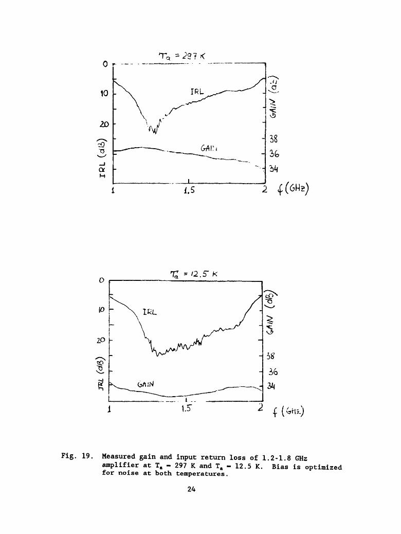
An example of measured gain and input return loss is shown in Figure 19. The values of input return loss are sufficiently large for the amplifier to be used in a front-end without an input isolator. Output return loss is also large (> 15 dB). All characteristics show good agreement with model predictions.
21
200
150 -
c
100
50
0
-i r
Tn MEASURED
Tn MODEL MERS. Gain
Tamb=297 K
1 ^,--,,J,,^-i-r: i
40
30
20
m T5
rd
10
0 1.0 1.5 F CGHzD 2.0
Fig. 15. Measured and predicted characteristics of 1.2-1.8 GHz amplifier at Ta - 297 K (S/N L-2, MGFC4404 MODFET's).
20
15
10 -
0
-i r
\
Tn MERSURED
Tn MODEL MERS. Gain
Tamb=12.5 K
i-~--+~-™P"'' ■ «
40
30
20
10
0
m
fd
1.0 1.5 F CGHz] 2.0
Fig. 16. Measured and predicted characteristics of 1.2-1.8 GHz amplifier at Ta - 12.5 K (S/N L-2, MGFC4404 MODFET's).
22
10
5 -
0
1 i r-
T« MTQCI lorn
—i i 1 1
i ri i iuruui\i_jj /
.\ _ Tn MODEL / - A
A • A
/ / .'
"A Tannb = = 4 .2 K A" "
/ . -r/ •
_ \
T T
/
r ./■■'
r/
•v' ■ • ■
S A. ..•■/
L -
1.0 1.5 F CGHz] 2.0
Fig. 17. Measured and predicted noise of 1.2-1.8 GHz amplifier at Ta - 4.2 K (S/N L-2, MGFC4404 MODFET's)
^L
N0I5E TEMP. vs. RMBIENT TEMP.
50
40
30
20
10
0
i—i i i i | i i i—i—| i i i i | i i i
v
A
,* ..*
A /+ /+
+ V A' A ,-'+
+>' +--'
.-■F ;K >'
>'"
.--+
J i ■ ■ ■ ' * ■ * * I ■ ■ ■ i I
0 50 100 150 200 250 300
Tamb [K]
Fig. 18. Cooling curve of a typical L-band HEMT amplifier (S/N L-l, FHR02X's, room temperature optimal bias).
23
T^ -221 <
$ (6H2)
O r
$L
nz * as K
'Ky^1
hfwH
15
*
\3>
5^
2^
2 { (^)
Fig. 19. Measured gain and input return loss of 1.2-1.8 GHz amplifier at Ta - 297 K and T. - 12.5 K. Bias is optimized for noise at both temperatures.
24
6. Discussion and Conclusions
This report covered the design, modeling and realization of the cryogenically-coolable, L-band amplifier. The use of computer-aided design techniques and wideband noise model of a MODFET yielded an amplifier with nearly "optimal," within other design constraints, noise bandwidth performance. The amplifier also exhibited excellent gain flatness, stability and low input and output reflections.
The agreement between the measured and predicted noise temperature of the amplifier is excellent. The typical measured and predicted noise temperature in the band center at Ta - 12.5 K is about 2.8 K. Out of that, about 1.2 K is attributed to the device itself and an additional .5 K is contributed by the stabilization resistor in the drain and the subsequent stages. The remaining balance of 1.1 K is attributable to the losses in the input circuit and noise "mismatch" necessary for wideband design. It is, therefore, not necessary to invoke the presence of trap related 1/f noise and/or G-R noise to explain the measured performance of the amplifier in L-band which validates the assumption of the wideband noise model of a FET [6], [7]. If, in fact, these noise sources are present, their influence is considerably smaller than the error in measurement and the error in estimation of losses in the amplifier input circuit.
It is possible to foresee slight improvement (< 1 K) in amplifier noise temperature with the use of superconducting input matching circuits and employing more sophisticated stabilization and bias circuit contributing less noise to the overall amplifier performance.
ACKNOWLEDGEMENTS
The contributions of Ron Harris and William Lakatosh to the development of amplifier manufacturing procedures are gratefully acknowledged. Dylon Dillon expertly manufactured the mechanical parts. Dr. S-K. Pan performed noise temperature measurement at ambient temperature of 4.2 K. J. D. Gallego gratefully acknowledges the financial support provided by the Centro Astronomico de Yebes, Institute Geografico Nacional, Guadalajara, Spain.
25
REFERENCES
[I] S. Weinreb, D. Fenstermacher, and R. Harris, "Ultra Low-Noise, 1.2- 1.7 GHz, Cooled GaAs FET Amplifiers," Electronics Division Internal Report No. 220, National Radio Astronomy Observatory, Charlottesville, VA, September 1981. (Also in IEEE Trans, on MTT, vol. MTT-30, pp. 849-853, June 1982.)
[2] Chanlong Xu, "Low-Noise, 1.25 GHz, Cooled, HEMT Amplifier," Electronics Division Technical Note No. 151, National Radio Astronomy Observatory, Charlottesville, VA, April 1989.
[3] Model LTE 1141, Passive Microwave Technology, Canoga Park, CA 91304.
[4] D. L. Fenstermacher, "A Computer-Aided Analysis Routine Including Optimization for Microwave Circuits and Their Noise," Electronics Division Internal Report No. 117, National Radio Astronomy Observatory, Charlottesville, VA, July 1981.
[5] J. Granlund, "FARANT on the HP 9816 Computer," Electronics Division Internal Report No. 250, National Radio Astronomy Observatory, Charlottesville, VA, July 1984.
[6] M. W. Pospieszalski, "Modeling of Noise Parameters of FET's and MODFET's and Their Frequency Dependence," IEEE Trans, on MTT, vol. MTT-37, pp. 1340-1350, Sept. 1989.
[7] M. W. Pospieszalski, "A New Approach to Modeling of Noise Parameters of FET's and MODFET's and Their Frequency and Temperature Dependence," National Radio Astronomy Observatory Electronics Division Internal Report No. 279, Charlottesville, VA, July 1988.
[8] Alain Cappy, "Noise Modeling and Measurement Techniques," IEEE Trans, on MTT, vol. MTT-36, pp. 1-10, January 1988.
[9] RT/Duroid 6010.5 ceramic polytetrafluoroethylene composite, 1 oz. Cu both sides, 0.050" thick, Rogers Corp., Microwave Materials Div., Box 3000, Chandler, AZ 85244.
[10] J. D. Woermbke, "Soft Substrates Conquer Hard Designs," Microwaves, vol. 21, 1, pp. 89-98, January 1982.
[II] K. C. Gupta, Computer-Aided Design of Microwave Circuits, Artech House, 1981, pp. 183-193.
[12] J. D. Gallego, "HP 8510 Network Analyzer Data Acquisition by FARANT," Electronics Division Technical Note No. 157, National Radio Astronomy Observatory, Charlottesville, VA, December 1989.
26
[13] R. A. Pucel, D. J. Masse, C. P. Hartwig, "Losses in Microstrip," IEEE Trans, on MTT, vol. MTT-16, no. 6, pp. 342-350, June 1968.
[14] E. J. Denlinger, "Losses of Microstrip Lines," IEEE Trans, on MTT, vol. MTT-28, no. 6, pp. 513-522, June 1980.
[15] "Noise Figure Measurement Accuracy," Hewlett-Packard Application Note 57-2.
[16] M. W. Pospieszalski, J. D. Gallego, and W. J. Lakatosh, "Broadband, Low-Noise, Cryogenically-Coolable Amplifiers in 1 to 40 GHz Range," in the Proc. 1990 MTT-S Int. Microwave Symp., pp. 1253-1256, Dallas, TX, May 1990.
[17] P. L. D. Abrie, The Design of Impedance Matching Networks for Radio Frequency and Microwave Amplifiers, Artech House, Inc., 1985. Chapter III.
[18] American Technical Ceramics Corp.
[19] J. D. Gallego and M. W. Pospieszalski, "Accuracy of Noise Temperature Measurement of Cryogenic Amplifiers," Electronics Division Internal Report No. 285, National Radio Astronomy Observatory, Charlottesville, VA, March 1990.
[20] FHR02FH, FHR02X data sheets, Fujitsu, 1988.
[21] American Technical Ceramics data sheets, 1988.
[22] S. Weinreb, A. R. Kerr, private communication.
[23] S.-K. Pan, A. R. Kerr, M. J. Feldman, A. W. Kleinsasser, J. W. Stasiak, R. L. Sandstrom, and W. J. Gallagher, "An 85-116 GHz SIS Receiver Using Inductively Shunted Edge-Junctions," IEEE Trans, on MTT, vol. MTT-37, pp. 580-592, March 1989.
27
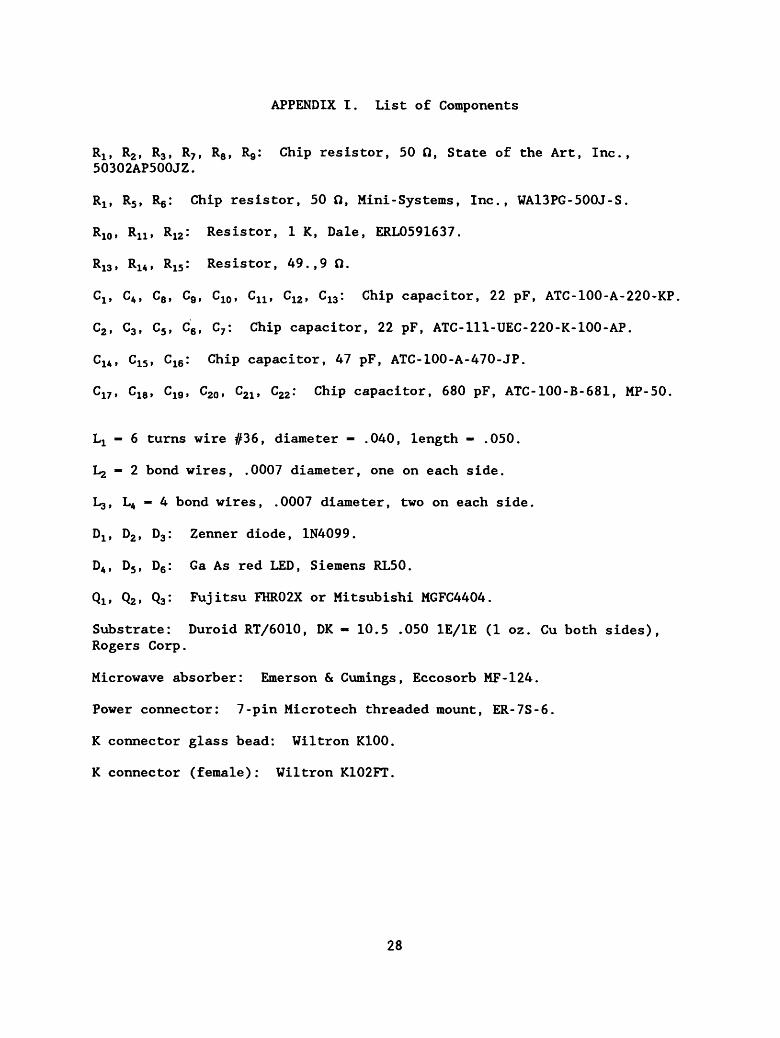
APPENDIX I. List of Components
Rlf R2, R3, R7, Rs, Rgi Chip resistor, 50 0, State of the Art, Inc., 50302AP500JZ.
Rlf R5, Re: Chip resistor, 50 0, Mini-Systems, Inc., WA13PG-500J-S.
R10, Rn, R^: Resistor, 1 K, Dale, ERL0591637.
Ri3» Ru» Ri5: Resistor, 49.,9 0.
C^ C4, C8, C9, C10, CU, C12, C13: Chip capacitor, 22 pF, ATC-100-A-220-KP,
C2, C3, C5, C6, C7: Chip capacitor, 22 pF, ATC-111-UEC-220-K-100-AP.
ci4» ci5» ci6: Chip capacitor, 47 pF, ATC-100-A-470-JP.
ci7» C18, C^, C20, C21, C22: Chip capacitor, 680 pF, ATC-100-B-681, MP-50.
Li - 6 turns wire #36, diameter - .040, length - .050.
L2 — 2 bond wires, .0007 diameter, one on each side.
L3, L4 - 4 bond wires, .0007 diameter, two on each side.
Di. D2, D3: Zenner diode, 1N4099.
DA, D5, D6: Ga As red LED, Siemens RL50.
Qi. Q2» Q3: Fujitsu FHR02X or Mitsubishi MGFC4404.
Substrate: Duroid RT/6010, DK - 10.5 .050 IE/IE (1 oz. Cu both sides), Rogers Corp.
Microwave absorber: Emerson & Cumings, Eccosorb MF-124.
Power connector: 7-pin Microtech threaded mount, ER-7S-6.
K connector glass bead: Wiltron K100.
K connector (female): Wiltron K102FT.
28
2.420 2.220
1.920 1.500
■ 1.210 1.182
1.000 .300 — £00 — H
—©-
—©•
—©•
—©-
-©■
■©■
■©■
-©—©■
-© ©■
■©•
#2-56 SCREWS (AMPLIFIER IS MOUNTED FROM THE BACK USING SAME HOLES)
MICROTECH 7 PIN ER-7S-6
i—i—r
.490
1.110
3.240
1.440 1.500
c
I
.683 — - .583 - — .500
— .250
^ V
S 0
T" .275
.800
HEMT LIGHT BOARD
l.g-1.8 GHz AMPLIFIER OUTLINE
J. D. GALLEGO 2-90