Embed Size (px)
Citation preview
THE INTERNATIONAL TECHNOLOGY ROADMAP FOR SEMICONDUCTORS: 2011
INTERNATIONAL
TECHNOLOGY ROADMAP
FOR
SEMICONDUCTORS
2011 EDITION
MICRO-ELECTRO-MECHANICAL SYSTEMS
(MEMS)
THE ITRS IS DEVISED AND INTENDED FOR TECHNOLOGY ASSESSMENT ONLY AND IS WITHOUT REGARD TO ANY
COMMERCIAL CONSIDERATIONS PERTAINING TO INDIVIDUAL PRODUCTS OR EQUIPMENT.
THE INTERNATIONAL TECHNOLOGY ROADMAP FOR SEMICONDUCTORS: 2011
TABLE OF CONTENTS
MEMS ................................................................................................................................... 1
1 Scope ........................................................................................................................................ 1 1.1 Accelerometers ...................................................................................................................................... 4 1.2 Gyroscopes ............................................................................................................................................ 5 1.3 Microphones ........................................................................................................................................... 6 1.4 RF MEMS ............................................................................................................................................... 8
2 Difficult Challenges .................................................................................................................... 9 2.1 Accelerometers ...................................................................................................................................... 9 2.2 Gyroscopes .......................................................................................................................................... 10 2.3 Microphones ......................................................................................................................................... 10 2.4 RF MEMS ............................................................................................................................................. 10
3 Technology Requirements ........................................................................................................11 3.1 Accelerometers .................................................................................................................................... 12 3.2 Gyroscopes .......................................................................................................................................... 12 3.3 Microphones ......................................................................................................................................... 12 3.4 RF MEMS ............................................................................................................................................. 13
4 Potential Solutions ....................................................................................................................13 4.1 Design and Simulation ......................................................................................................................... 14 4.2 Packaging and Integration ................................................................................................................... 14 4.3 Test ...................................................................................................................................................... 15
5 Cross-Cut Issues ......................................................................................................................16 5.1 Assembly And Packaging .................................................................................................................... 16 5.2 Test ...................................................................................................................................................... 16 5.3 RF and Analog Mixed Signal ............................................................................................................... 16
6 Emerging MEMS for Mobile Applications ..................................................................................16 6.1 Optical Filters ....................................................................................................................................... 16 6.2 Picoprojector ........................................................................................................................................ 17 6.3 Electronic Nose .................................................................................................................................... 18 6.4 Microspeakers ...................................................................................................................................... 21 6.5 Ultrasound Devices .............................................................................................................................. 22
7 Conclusions ..............................................................................................................................23
8 References ...............................................................................................................................25
THE INTERNATIONAL TECHNOLOGY ROADMAP FOR SEMICONDUCTORS: 2011
LIST OF FIGURES
Figure MEMS1 The combined need for digital and non-digital functionalities in an integrated system is translated as a dual trend in the International Technology Roadmap for Semiconductors: miniaturization of the digital functions (“More Moore”) and functional diversification (“More-than-Moore”).8 .................................................................................... 2
Figure MEMS2 Path of increasing integration beginning with mainframe computers to minicomputers, PCs, desktop internet, and to mobile internet devices such as smartphones and tablet computers. ................................................. 3
Figure MEMS3 Unit shipments for motion sensors in handsets and tablets are forecasted to reach 1¾ billion by 2015. ......................................................... 4
Figure MEMS4 The MEMS accelerometer, introduced in the iPhone by Apple, enabled the functionality of automatic screen rotation. .................................. 5
Figure MEMS5 3-axis gyroscopes ......................................................................................... 6
Figure MEMS6 CMOS MEMS Microphone Die and Packaged Microphones ......................... 7
Figure MEMS7 The Si Time SiT9104 provides six single-ended clock outputs, two from each PLL, which can operate at up to 220 MHz. Each PLL and associated pair of clock outputs can be driven by independent voltage supplies (1.8, 2.5, 2.8 or 3.3 V), and each output pair on the differential output SiT9103 can be configured to one of three signaling levels, LVPECL, LVDS or CML. ................................................................................ 8
Figure MEMS8 A MEMS Narrow Band Tunable Filter.16 ...................................................... 17
Figure MEMS9 TI’s prototype USB picoprojector nHD Pico with 20 lumens, 640 x 360 resolution, a contrast ratio greater than 1,000:1, a true RGB LED wide color gamut and reliance on a low-power Pico DPP2601 2607 ASIC processor. ................................................................. 18
Figure MEMS10 (a) Schematic cross-section of a capacitive micromachined ultrasound transducer (cMUT), (b) SEM detail of four dual thickness cMUT cells from a 2D array of acoustic pixels, and (c) COMSOL simulation of the first eienmode of a dual thickness cMUT cell. .................. 22
LIST OF TABLES
Table MEMS1 MEMS Accelerometer Technology Requirements (LINK) ............................ 12
Table MEMS2 MEMS Gyroscope Technology Requirements (LINK) .................................. 12
Table MEMS3 MEMS Microphone Technology Requirements (LINK) ................................ 13
Table MEMS4 RF MEMS Resonator Technology Requirements (LINK) ............................. 13
Table MEMS5 RF MEMS Galvanic Switch Technology Requirements (LINK) .................... 13
Table MEMS6 RF MEMS Varactors Technology Requirements (LINK) .............................. 13
Table MEMS7 Sensing Technologies Suitable for Electronic Nose Devices ....................... 20

MEMS 1
THE INTERNATIONAL TECHNOLOGY ROADMAP FOR SEMICONDUCTORS: 2011
MEMS “It is not enough that you should understand about applied science in order that your work may increase man's blessings.
Concern for the man himself and his fate must always form the chief interest of all technical endeavors; concern for the
great unsolved problems of the organization of labor and the distribution of goods in order that the creations of our mind
shall be a blessing and not a curse to mankind. Never forget this in the midst of your diagrams and equations.”
− Albert Einstein (1879 - 1955)
1 SCOPE
The ITRS MEMS Technology Working Group (TWG) was established is 2011 and tasked to develop a new chapter for
the ITRS Roadmap. The motivation for this endeavor can be traced back to the MEMS Industry Group’s (MIG) 2010
METRIC Workshop on MEMS Fabrication Challenges, held in San Jose, CA, in March 2010. An important outcome
from this workshop was the recognition that device testing, which can typically consume 20% to as much as 70% of the
manufacturing cost, was a growing area of concern for the industry. MIG’s members decided to assess the current
practices and needs for device testing, and to organize a workshop on the subject in the following year.
This outcome fueled the establishment of an iNEMI MEMS TWG in the summer of 2010, which delivered its report to
iNEMI in November 2010. This report was published as the MEMS/Sensors Chapter in the 2011 iNEMI Roadmap [1]. As
iNEMI and ITRS have developed a partnership, a proposal for forming an ITRS MEMS TWG was presented to the
International Roadmapping Committee (IRC) at the ITRS’ Winter Meeting on December 1, 2010, in Tsukuba, Japan, and
was approved as a pilot effort. The ITRS MEMS TWG presented a progress report at the ITRS Spring Meeting on April
11, 2011, in Potsdam, Germany, and was approved to become a formal committee that would produce a MEMS Chapter
in the upcoming 2011 ITRS Report.
This report incorporates information from the iNEMI report with a focus on Mobile Internet Devices (such as smart
phones and table computers), and adds the well-known Technology Requirements Tables, which are a main characteristic
of ITRS technology roadmapping.
Micro-Electro-Mechanical Systems (MEMS) are devices that are fabricated using techniques similar to those used for
integrated circuits (ICs). They are composed of micrometer-sized mechanical structures (suspended bridges, cantilevers,
membranes, fluid channels, etc.) and often integrated with analog and digital circuitry. MEMS can act as sensors,
receiving information from their environment, or as actuators, responding to a decision from the control system to change
the environment.
MEMS are often said to have been inspired more than 50 years ago with the famous lecture of Richard Feynman in 1959
entitled “There’s plenty of room at the bottom” [2], where the “bottom” is referred to as exploring the reduction of length
scale to enable new functions. However, manufacturing firms like Kulite (1958) had already been focusing on developing
new sensor technologies based on MEMS that preceded Feynman’s seminal talk. The miniaturization of
electromechanical devices composed of suspended membranes and movable structures appeared in the 60’s [3] and further
developed in the 70’s and based on the “bulk” micromachining method, which released the elements by etching away the
silicon substrate material. The surface micromachining method as we know it today was first demonstrated by Howe and
Muller in the early 80’s and relied on polysilicon as the structural material [4].
MEMS technology is perceived as a child or ancillary innovation of semiconductor electronics, much as how information
technology is an ancillary innovation. But unlike semiconductor electronics, MEMS are not driven by a small set of
applications, such as microprocessors and memories, but by literally hundreds if not thousands of unique devices and
applications. The diversity of MEMS applications, manufacturing techniques, materials, and a lack of a unit cell such as
the CMOS transistor, have resulted in MEMS technologies as being thought of as a job shop rather than like a high-
volume semiconductor factory. Although there has been much earlier work in roadmapping MEMS technologies [5], the
historical lack of cohesiveness in the industry has made it a challenge for obtaining industry-wide consensus on
crosscutting needs.
Similar to discrete sensor technologies, Micro-Electro-Mechanical Systems (MEMS) have an extremely diverse
application set, ranging from physical to optical, chemical, and biological, as well as a diversity of materials and methods
used to manufacture them. A first impression of MEMS would undoubtedly start with the theme of miniaturization for
2 MEMS
THE INTERNATIONAL TECHNOLOGY ROADMAP FOR SEMICONDUCTORS: 2011
realizing ever-smaller sensors and actuators. However, where they truly stand apart is in the integration of functionalities:
combining sensing and actuation with information processing, signal conditioning, built-in test, and communications.
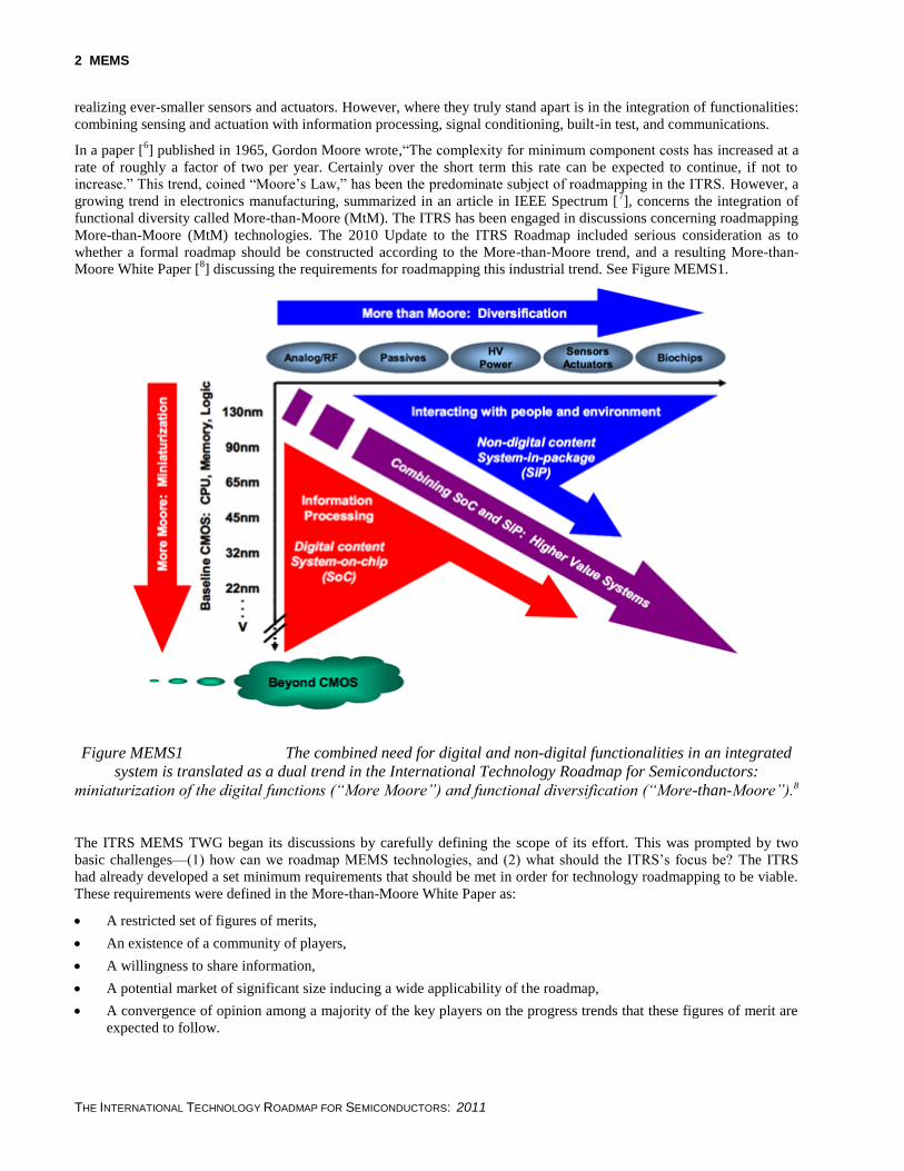
In a paper [6] published in 1965, Gordon Moore wrote,“The complexity for minimum component costs has increased at a
rate of roughly a factor of two per year. Certainly over the short term this rate can be expected to continue, if not to
increase.” This trend, coined “Moore’s Law,” has been the predominate subject of roadmapping in the ITRS. However, a
growing trend in electronics manufacturing, summarized in an article in IEEE Spectrum [7], concerns the integration of
functional diversity called More-than-Moore (MtM). The ITRS has been engaged in discussions concerning roadmapping
More-than-Moore (MtM) technologies. The 2010 Update to the ITRS Roadmap included serious consideration as to
whether a formal roadmap should be constructed according to the More-than-Moore trend, and a resulting More-than-
Moore White Paper [8] discussing the requirements for roadmapping this industrial trend. See Figure MEMS1.
Figure MEMS1 The combined need for digital and non-digital functionalities in an integrated
system is translated as a dual trend in the International Technology Roadmap for Semiconductors:
miniaturization of the digital functions (“More Moore”) and functional diversification (“More-than-Moore”).8
The ITRS MEMS TWG began its discussions by carefully defining the scope of its effort. This was prompted by two
basic challenges—(1) how can we roadmap MEMS technologies, and (2) what should the ITRS’s focus be? The ITRS
had already developed a set minimum requirements that should be met in order for technology roadmapping to be viable.
These requirements were defined in the More-than-Moore White Paper as:
A restricted set of figures of merits,
An existence of a community of players,
A willingness to share information,
A potential market of significant size inducing a wide applicability of the roadmap,
A convergence of opinion among a majority of the key players on the progress trends that these figures of merit are
expected to follow.
MEMS 3
THE INTERNATIONAL TECHNOLOGY ROADMAP FOR SEMICONDUCTORS: 2011
Many of these requirements were already ripening in the MEMS industry. The MEMS Industry Group represented an
existence of a community of players with a willingness to share information to address a common need: the rising cost of
device testing and a decision to hold a workshop on this topic to solve this problem. There was also a market of
significant size: MEMS device manufacturing was forecasted to grow rapidly in consumer electronics-related
applications. iSuppli had forecasted growth of almost 30% compounded annually [9] in smart phones and tablet
computers. Lastly, there was a demonstrated potential to reach a convergence of opinion by the recent success of the
MEMS Chapter in the 2011 iNMEI Report.
The second challenge, what should be the ITRS’s focus for MEMS roadmapping, was critical for facilitating an industrial
consensus to meet the final requirement for a convergence of opinion on a restricted set of figures of merit, e.g., the
technology requirements tables. MEMS technologies are quite diverse, ranging from microheating elements, surgical
tools, and microfluidic devices, as well as the better-known applications of inkjet printer cartridges, acceleration sensors,
and digital light projectors. In contrast to this diversity, the ITRS is perceived to have a very specific focus: roadmapping
the technological growth of the microprocessor and memory. Though there had been much thought within the ITRS on
the evolution of Moore’s Law to include functional diversity and MtM Roadmapping, there were still many questions
within the ITRS membership concerning how this would be accomplished for a technology as diverse as MEMS. Thus, it
was very important that a correct alignment developed to quell concerns about the diversity of MEMS both within the
ITRS and also with potentially new MEMS industrial members.
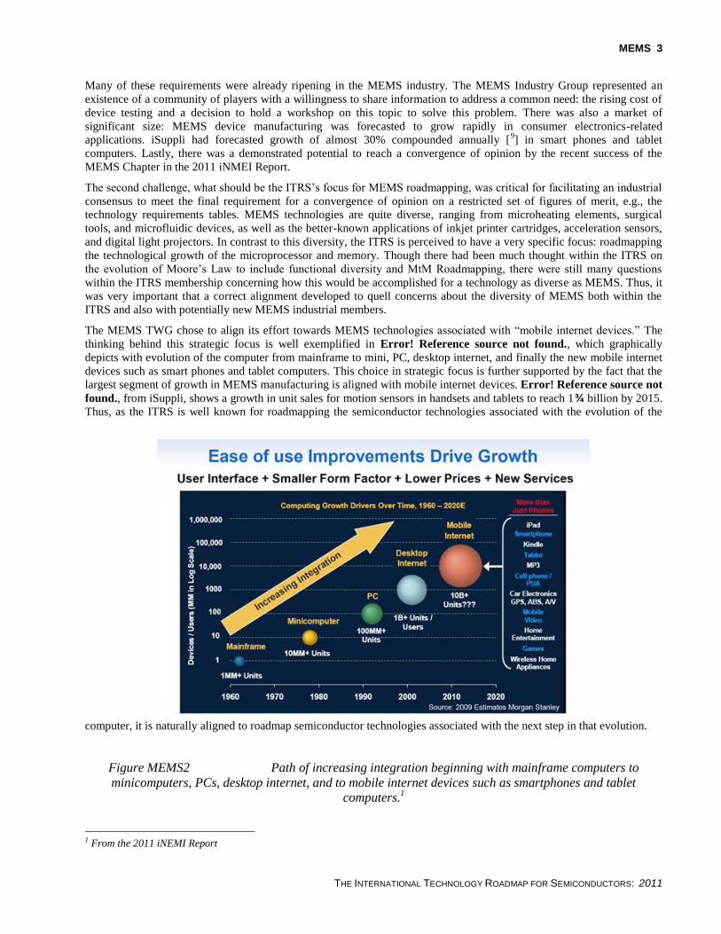
The MEMS TWG chose to align its effort towards MEMS technologies associated with “mobile internet devices.” The
thinking behind this strategic focus is well exemplified in Error! Reference source not found., which graphically
depicts with evolution of the computer from mainframe to mini, PC, desktop internet, and finally the new mobile internet
devices such as smart phones and tablet computers. This choice in strategic focus is further supported by the fact that the
largest segment of growth in MEMS manufacturing is aligned with mobile internet devices. Error! Reference source not
found., from iSuppli, shows a growth in unit sales for motion sensors in handsets and tablets to reach 1¾ billion by 2015.
Thus, as the ITRS is well known for roadmapping the semiconductor technologies associated with the evolution of the
computer, it is naturally aligned to roadmap semiconductor technologies associated with the next step in that evolution.
Figure MEMS2 Path of increasing integration beginning with mainframe computers to
minicomputers, PCs, desktop internet, and to mobile internet devices such as smartphones and tablet
computers.1
1 From the 2011 iNEMI Report

4 MEMS
THE INTERNATIONAL TECHNOLOGY ROADMAP FOR SEMICONDUCTORS: 2011
Figure MEMS3 Unit shipments for motion sensors in handsets and tablets are forecasted to
reach 1¾ billion by 2015.2
The adoption of this strategic focus for the ITRS MEMS TWG’s roadmapping effort was the key to reaching the buy-in,
both within the ITRS and with the MEMS industry, for moving forward. Mobile internet devices contain MEMS devices
such as accelerometers and gyroscopes, microphones, and also have radios (WiFi and cellular) that have application needs
for RF MEMS devices, including resonators, varactors, and switches.
There are also a number of emerging MEMS technologies that have potential for future incorporation in mobile devices.
These include optical filters to improve cameras, picoprojectors, for viewing pictures and presentations on large screens,
the electronic nose, microspeakers, and ultrasound devices. These applications are covered in Section 6, Emerging MEMS
for Mobile Applications, as a detailed review of the topics to be used as a means for determining when new devices
technologies should be included in our roadmapping efforts.
1.1 ACCELEROMETERS
The English physicist George Atwood (1746-1807) invented the accelerometer in 1783. Accelerometers have now been in
use for almost a century, with the use of resistance-bridge-type accelerometers finding application in bridges,
dynamometers, and aircraft [10
]. MEMS accelerometers were proposed in 1979 in a paper on a batch-fabricated silicon
accelerometer [11
]. The early commercial MEMS accelerometers were of the piezoresistive type realized by silicon bulk
micromachining. However, the advent of surface micromachining and capacitive sensing technologies in the late 1980’s
and early 1990’s took MEMS accelerometers to their first major commercial success in automotive applications. By the
late 1990’s, expedited by the more stringent automotive safety regulations, the adoption of MEMS accelerometers for
airbag crash sensing in automobiles was wide spread. During the 2000’s, automotive accelerometer applications further
widened to rollover detection and electronic stability controls, among other functions. Adoption was slow, however, for
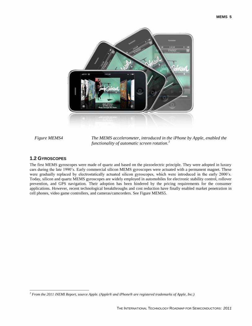
the consumer motion and tilt sensing applications until the price, size, and power consumption of MEMS accelerometers
were finally in line with market requirements toward the late 2000’s. The shipment of the Nintendo Wii and the Apple
iPhone, each equipped with a 3-axis MEMS accelerometer, were landmark events, pioneering the ubiquitous usage of
MEMS accelerometers in consumer handheld products. Today, a 3-axis MEMS accelerometer is increasingly employed
in conjunction with a 3-axis magnetometer for personal navigation or with a 3-axis MEMS gyroscope to constitute an
IMU (Inertial Measurement Unit) to fulfill the needs for complete motion sensing. See Figure MEMS4.
2 From iSuppli’s MIG Webinar presentation “A Global Analysis of the Current MEMS Market” on July 27, 2011
MEMS 5
THE INTERNATIONAL TECHNOLOGY ROADMAP FOR SEMICONDUCTORS: 2011
Figure MEMS4 The MEMS accelerometer, introduced in the iPhone by Apple, enabled the
functionality of automatic screen rotation.3
1.2 GYROSCOPES
The first MEMS gyroscopes were made of quartz and based on the piezoelectric principle. They were adopted in luxury
cars during the late 1990’s. Early commercial silicon MEMS gyroscopes were actuated with a permanent magnet. These
were gradually replaced by electrostatically actuated silicon gyroscopes, which were introduced in the early 2000’s.
Today, silicon and quartz MEMS gyroscopes are widely employed in automobiles for electronic stability control, rollover
prevention, and GPS navigation. Their adoption has been hindered by the pricing requirements for the consumer
applications. However, recent technological breakthroughs and cost reduction have finally enabled market penetration in
cell phones, video game controllers, and cameras/camcorders. See Figure MEMS5.
3 From the 2011 iNEMI Report, source Apple. (Apple® and iPhone® are registered trademarks of Apple, Inc.)

6 MEMS
THE INTERNATIONAL TECHNOLOGY ROADMAP FOR SEMICONDUCTORS: 2011
Figure MEMS5 3-axis gyroscopes4
1.3 MICROPHONES
For fifty years, acoustic components such as microphones, speakers and transducers had remained fundamentally
unchanged. One such component, the Electret Condenser Microphone (ECM), has been used in billions of portable
electronic devices such as mobiles phones and portable computers (laptops, netbooks, tablets, etc.). An explosion of new
technologies enabled a compelling array of new features in smaller form factors in the 90’s, and at the same time mobile
phones and notebook computers evolved into more complex and powerful multimedia devices that needed to support real-
time audio and video communications in a wide range of environments ranging from hotel rooms to rock concerts. These
new use-cases needed small, thin, well-matched microphones that could be assembled with the rest of the device in the
standard automated manufacturing line. Though MEMS microphones had been demonstrated, it was not until it became
clear that the changing acoustic requirements in consumer electronic devices were pushing beyond the limits of ECM
technology, and device designers and manufacturers began to look towards MEMS microphones to meet their needs.
MEMS microphones offered many benefits over ECMs that allowed device manufacturers to meet the more stringent
needs of their customers. The first silicon microphones were adopted for two main reasons—(1) silicon microphones are
smaller in size than ECMs while having the same or better acoustic performance and (2) silicon microphones also have
the advantage over ECMs that they are compatible with automated IC assembly equipment, improving manufacturing
throughput and yield. These features were the main drivers of the first major wave of analog-output silicon microphone
adoption in mobile phones that occurred in 2003-2005.
The first digital-output MEMS microphones were introduced in 2006. Portable computer manufacturers were the first to
adopt the digital-output MEMS microphones - not only because they were thin and surface-mountable, but also because
for the first time, designers were able to position the microphone in the bezel of the laptop (the best acoustic location) and
run the audio traces around the screen and down into the base of the laptop without using thick shielded cabling for
protection from radio frequency (RF) and electromagnetic (EM) interference.
Analog and digital-output microphones have continued to both shrink in size and advance acoustic performance, and as a
result have increasingly become adopted in the mobile phone and laptop market. Many laptops now contain a digital
microphone array in the bezel with the camera for VoIP communications, and recently, some mobile phones have been
introduced that use two or more microphones for noise suppression. These applications along with new market areas such
as wired and wireless headsets have helped push the forecast for MEMS microphones to above 1B units in 2013 (iSuppli,
February 2010).
The first silicon microphones were multi-chip-modules with one transducer chip and a second IC containing a pre-
amplifier and/or an analog-to-digital converter. These two devices are then wire-bonded to each other within the MEMS
4 From MIG’s MEMS blog Contributed by Laurent Robin, MEMS Analyst, Yole Développement, photo source InvenSense
MEMS 7
THE INTERNATIONAL TECHNOLOGY ROADMAP FOR SEMICONDUCTORS: 2011
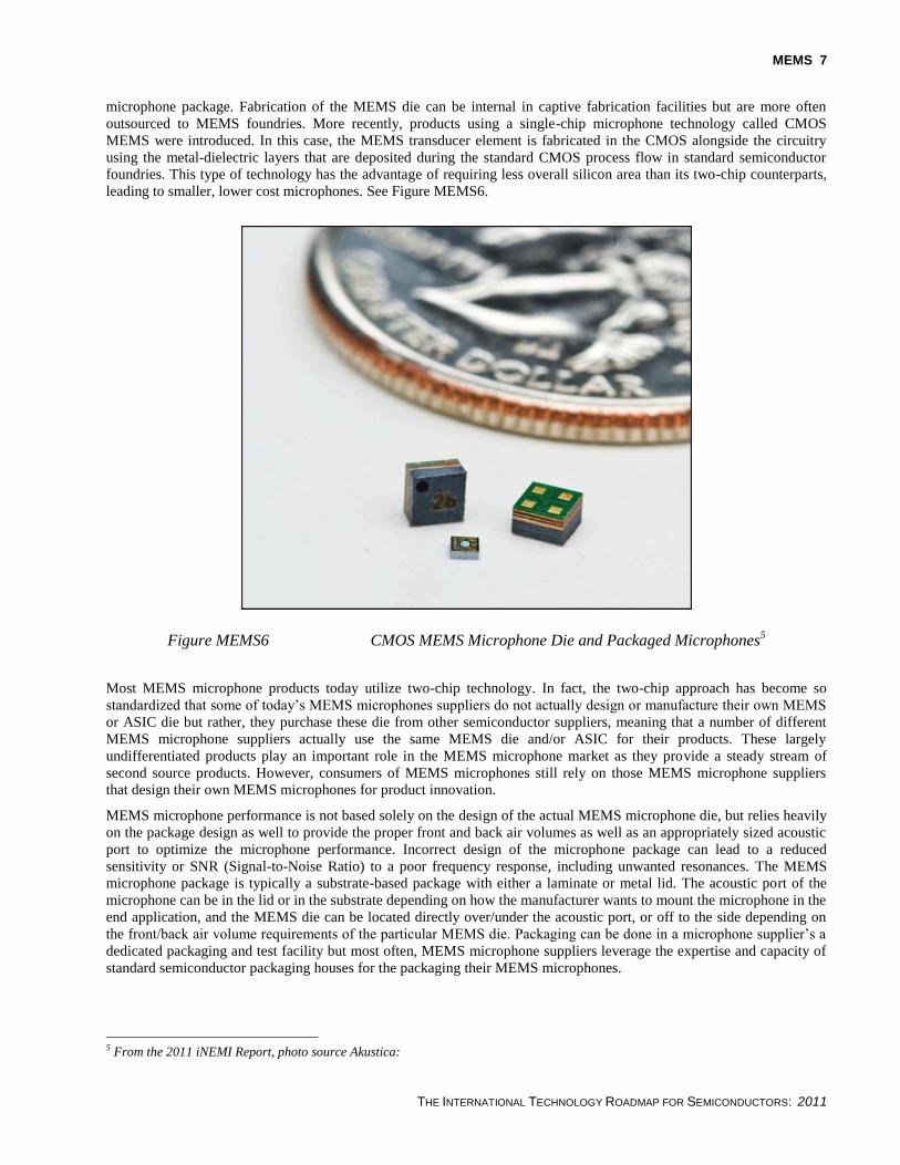
microphone package. Fabrication of the MEMS die can be internal in captive fabrication facilities but are more often
outsourced to MEMS foundries. More recently, products using a single-chip microphone technology called CMOS
MEMS were introduced. In this case, the MEMS transducer element is fabricated in the CMOS alongside the circuitry
using the metal-dielectric layers that are deposited during the standard CMOS process flow in standard semiconductor
foundries. This type of technology has the advantage of requiring less overall silicon area than its two-chip counterparts,
leading to smaller, lower cost microphones. See Figure MEMS6.
Figure MEMS6 CMOS MEMS Microphone Die and Packaged Microphones5
Most MEMS microphone products today utilize two-chip technology. In fact, the two-chip approach has become so
standardized that some of today’s MEMS microphones suppliers do not actually design or manufacture their own MEMS
or ASIC die but rather, they purchase these die from other semiconductor suppliers, meaning that a number of different
MEMS microphone suppliers actually use the same MEMS die and/or ASIC for their products. These largely
undifferentiated products play an important role in the MEMS microphone market as they provide a steady stream of
second source products. However, consumers of MEMS microphones still rely on those MEMS microphone suppliers
that design their own MEMS microphones for product innovation.
MEMS microphone performance is not based solely on the design of the actual MEMS microphone die, but relies heavily
on the package design as well to provide the proper front and back air volumes as well as an appropriately sized acoustic
port to optimize the microphone performance. Incorrect design of the microphone package can lead to a reduced
sensitivity or SNR (Signal-to-Noise Ratio) to a poor frequency response, including unwanted resonances. The MEMS
microphone package is typically a substrate-based package with either a laminate or metal lid. The acoustic port of the
microphone can be in the lid or in the substrate depending on how the manufacturer wants to mount the microphone in the
end application, and the MEMS die can be located directly over/under the acoustic port, or off to the side depending on
the front/back air volume requirements of the particular MEMS die. Packaging can be done in a microphone supplier’s a
dedicated packaging and test facility but most often, MEMS microphone suppliers leverage the expertise and capacity of
standard semiconductor packaging houses for the packaging their MEMS microphones.
5 From the 2011 iNEMI Report, photo source Akustica:

8 MEMS
THE INTERNATIONAL TECHNOLOGY ROADMAP FOR SEMICONDUCTORS: 2011
1.4 RF MEMS
RF MEMS devices include thin-film bulk-acoustic wave resonators (FBAR), surface acoustic wave resonators (SAW),
resonators (timing devices), capacitive switches/varactors, and metal contact switches. In general, these device types have
found or will find use in wireless communication products as discrete devices, e.g., a FBAR filter mounted to a board or
mother chip, or a Si MEMS oscillator replacing a quartz part in an existing socket. The performance of the MEMS
discrete parts is typically on par or better than the previous generation product (MEMS or non-MEMS). Its low cost
allowed rapid adoption. The rate of adoption for parts that have greater performance benefits, but no clear cost benefits,
tend to be slower due to various economic factors and to technology maturity and demonstrated reliability of the existing
part that the MEMS part would replace. One example of the latter is the reliability of the packaged parts containing
MEMS switches (capacitive and metal contact). Market place introductions, when performance enabled new products
have no significant cost barriers compared to the desired function of the product, have been relatively rapid and assisted
by the use of existing, more mature MEMS process technology such as Si micromachining used in airbag sensors or
inkjet printers. The time at which the RF MEMS devices are produced in high-volumes often occurs when the MEMS
function is integrated with the CMOS, BiCMOS, or bipolar semiconductor die. The timing for this integration will be
primarily driven by cost. Until that time, initial introductions will occur in the following order: 1) favor discrete die (e.g.,
FBAR devices), 2) 3D stacking of the RF MEMS chip above or below the IC (e.g., variable capacitors), and 3) monolithic
integration with the IC, which will potentially reduce the bill of materials by removing customized MEMS packaging
from some devices and enable new applications due to integration and cost reduction.
The MEMS TWG has adopted 3 types of RF MEMS devices, which fit items classes 2 and 3 in the preceding paragraph:
resonator, varactor, and switch. These three are expected to find use in mobile internet devices, such as smart phones and
tablets, in the near term.
1.4.1 RF MEMS RESONATORS
There are number of companies trying to displace the traditional quartz oscillator with a Si-based MEMS oscillator for the
frequency reference used in clock and timing applications. The Si-based MEMS oscillator has the advantages in shock
resistance, smaller form factor and are more suitable for mass production. The MEMS oscillator can be also integrated
with the timing circuit into a much smaller package than the Quartz oscillator.
Figure MEMS7 The Si Time SiT9104 provides six single-ended clock outputs, two from each
PLL, which can operate at up to 220 MHz. Each PLL and associated pair of clock outputs can be driven by
independent voltage supplies (1.8, 2.5, 2.8 or 3.3 V), and each output pair on the differential output SiT9103
can be configured to one of three signaling levels, LVPECL, LVDS or CML.6
6 From Electronic Products published on July 22, 2011

MEMS 9
THE INTERNATIONAL TECHNOLOGY ROADMAP FOR SEMICONDUCTORS: 2011
1.4.2 RF MEMS SWITCHES
RF-MEMS contact switches hold great promise for improving performance and increasing the integration of the RF front-
end of wireless systems. RF-MEMS switches can provide far lower losses, higher isolation and higher linearity than their
solid-state counterparts. This is of increasing value as the number of bands and modes that must be supported in a mobile
platform continues to grow. Possible monolithic integration with standard CMOS brings the promise of low-cost and
small size. Many high-performance devices have been built using RF-MEMS including a wide range of switches.
However, none has yet reached commercial success, both due to remaining technical challenges and due to rapid
advances in more conventional switching technologies.
1.4.3 RF MEMS VARACTORS
RF-MEMS varactors and capacitive switches hold even greater promise for improving performance and increasing the
integration of the RF front-end of wireless systems. Instead of switching between sets of fixed elements, RF-MEMS
varactors can provide direct adjustability to the RF circuits and have loss performance similar to fixed passive elements.
This enables a simplification of the systems by a reduction in the multiplicity of signal paths. Achieving these benefits
requires more complex control than simple switching. Note that analog MEMS varactors are not practical in most
applications due to variability over temperature and influences of voltages induced by RF power. Practical RF-MEMS
varactors are typically formed from arrays of capacitive switches to provide the necessary reproducibility and robustness.
The technology is similar to RF-MEMS contact switches but with crucial differences. Monolithic integration with
standard CMOS is fundamentally easier and has already been accomplished. Capacitive switches are more robust to
switching under RF power and have significantly higher cycling lifetimes than contact switches.
2 DIFFICULT CHALLENGES A survey of R&D investment in MEMS technologies yields the observation that virtually all investment has been in the
front-end of manufacturing: device and process development. MEMS manufactures, as a result, have a diverse set of
methods and tools for MEMS device development and one might say that the know-how to make devices is available.
The MEMS devices considered in this report will generally see a continuous incremental increase in performance, and
decrease in package size and cost.
The greatest challenges for the MEMS technologies are related to their integration aspects, and are primarily linked to the
back-end of manufacturing, packaging and test. As mobile internet device manufacturers work to decrease size and
weight, extend battery life, and integrate new functionalities, their pull on MEMS device manufacturers is for smaller
package size and integration. The MEMS manufacturers refer to the integration of devices as multimode sensor
technologies. The challenge is to produce 10 degree-of-freedom (DOF) MEMS inertial measurement units (IMUs), which
incorporate 3-axis accelerometers, 3-axis gyroscopes, 3-axis magnetometers (compass), and a pressure sensor (altimeter).
The requirements 10 DOF multimode sensor technologies are creating challenges primarily at the back-end of
manufacturing.
2.1 ACCELEROMETERS
MEMS accelerometer chips are becoming increasingly commonplace with mobile Internet devices. They provide the
sensing capability for automatic screen rotation, and their use is expanding, including their growing use for game
applications.
MEMS 3-axis accelerometers manufactured for consumer electronic applications are expected to see continuous
incremental improvement in performance over time. The improvements are expected in resolution, bias, and drift, with
resolutions improving by a factor of 2 from 1000 g to 500 g by 2015. The biggest challenge for MEMS accelerometers
comes from the projected cost reductions, moving from $0.50 per die down to $0.20 per die by 2017.
The Global Positioning System (GPS) unit in many mobile devices is used to find a location and track movement, but an
inertial measurement unit (IMU) is required when GPS signals are unavailable, such as in tunnels, inside buildings, or
when electronic interference is present. The IMU would consist of a 3-axis accelerometer, a 3-axis gyroscope, a 3-axis
magnetometer (electronic compass), and a pressure sensor (altimeter). Current MEMS technology can produce an IMU at
the board level.
The greatest challenge that accelerometers face is the integration in the IMU at the package level, followed by integration
at the chip level.
10 MEMS
THE INTERNATIONAL TECHNOLOGY ROADMAP FOR SEMICONDUCTORS: 2011
2.2 GYROSCOPES
The inclusion of a gyroscope in mobile devices allows for the detection of more detailed movements by a user compared
to the traditional accelerometer included in earlier models, such as the first generation iPhone™, manufactured by Apple.
Compared to accelerometers, MEMS gyroscopes have faced significant technical challenges to become adopted into
mobile applications due to their extreme sensitivity to package stress effects and their requirements for high precision
large actuation and high quality vacuum packaging. As a result, commercialization lagged behind that for accelerometers
and the price for gyroscopes was also substantially higher.
Gyroscopes are expected to see a continuous incremental increase in performance, especially in the resolution and zero g
bias level. The major challenges for 3-axis gyroscopes are related to cost reduction and package size reduction. However,
as with the accelerometers, the most difficult challenges faced concern their integration in the IMU.
2.3 MICROPHONES
Since their introduction, MEMS microphones have continued to shrink in size and improve in performance, while at the
same time have been following a rapid price reduction curve as overall volumes have increased. The future trend is for
more of the same. Die shrinking, die stacking and chip scale packaging approaches will continue to lead to smaller and
smaller microphones over the next decade. At the same time, consumer electronic device manufacturers continue to
request higher performance microphones. Higher signal-to-noise (SNR) microphones are required, as microphones need
to satisfy more use-cases in a single mobile phone than ever before; mainly near-ear talking, speakerphone, and video
recording. Wider bandwidth microphones are also becoming more important to support wider bandwidth mobile phone
networks and laptop Voice-over-Internet-Protocol (VoIP) as well as video recording of both voice and music. Smaller
microphones are needed to support new applications in small form factor devices like mobile phones, which use more
than one microphone for stereo recording or noise suppression. Additionally, smaller microphones will be necessary to
support the aggressive cost down targets required by the high volume, price sensitive consumer electronics market,
especially as they adopt multiple microphones in a single device. Based on these future demands, microphone
manufactures will have to support a significant amount of technology innovation in the coming decade.
Microphones require distribution around the system for functionality (e.g., noise cancellation). For this reason, there is
not a pull to integrate multiple microphones in a single package. Instead, the push is for developing digital I/O interface to
reduce noise over long signal lines.
MEMS microphones are expected to see a continuous incremental increase in performance, while decreasing in size cost.
Integration for microphones is moving in the direction of advancing ASIC functionality and I/O.
2.4 RF MEMS
The incorporation of RF MEMS into mobile devices is intended to lower power dissipation by the radio and to lower the
chip count in the device.
RF MEMS are still in the process of increasing their reliability and lowering cost before they will be adopted in mobile
devices.
RF MEMS are expected to increase in performance and reliability. The biggest challenge in RF MEMS is enhancing
reliability and lifetime (e.g., # of operations). Some of the future performance metrics have no known solutions, e.g.,
signal isolation requirements.
2.4.1 RF MEMS RESONATORS
The MEMS resonator inherently has higher temperature expansion coefficient than the Quartz, therefore it would have
higher frequency drift over temperature if without a proper compensation. A proper temperature compensation scheme for
the MEMS resonator together with the timing circuit and low noise PLL are necessary in order to make a stable timing
reference. The MEMS oscillator products can be differentiated from the frequency ranges of applications and the level of
phase noise and jitters from the integrated solution. The major source of the phase noise and phase jitter comes from the
compensation loop and PLL circuit. These are the areas that draw the major development to up grade the performance of
the MEMS oscillator. For cell phone application, the power consumption is always a concern. This creates more
challenges to the design of the compensation and PLL circuit. There are few Si based MEMS oscillators that have the
phase noise and jitter within the 2ppm range and with reasonable low power for cell phone application.
2.4.2 RF MEMS SWITCHES
There are several key challenges to the commercialization of RF-MEMS switches. The foremost barrier is achieving a
cost low enough to be competitive with more conventional switching solutions. The prime cost driver is the hermetic or

MEMS 11
THE INTERNATIONAL TECHNOLOGY ROADMAP FOR SEMICONDUCTORS: 2011
possibly near-hermetic packaging required to protect the MEMS and contact surfaces from moisture and organic
contamination. This packaging must have minimal impact on the high RF performance and must be compatible with
standard semiconductor back-end flows. Another key cost element is the requirement for circuits to generate and control
the high voltages needed to minimize die size and maximize reliability. These circuits should consume negligible power,
provide a standard control interface and avoid introducing any RF interference. The final piece in the cost puzzle is
achieving high yield, ideally across 200mm wafers.
Another key challenge is clearly demonstrating the required reliability for the application use cases in the range of
environments where they will be applied. Sufficient lifetimes have been demonstrated for many applications on limited
sample quantities through direct long-term testing. These tests imply that RF-MEMS switch contact are capable of the
required reliability but such testing is not sufficient to establish a statistical basis for high volume defect projections,
especially over early life. While several accelerated reliability tests have been proposed, unfortunately none has yet
proven validity. The cycling reliability is particularly impacted by hot switching events. For mobile applications, new
solutions will be needed to enable contact switching at full power. Additional reliability limitations arise in some
technologies due to metal mechanical yield or creep under stress leading to irreversible behavior shifts as well as from
charging of dielectrics used to prevent actuator shorts.
A final challenge for some applications is achieving high reproducibility in the resistance between contact closures.
Residual films on the contact surfaces, especially organic, lead to increased variability.
2.4.3 RF MEMS VARACTORS
As with switches, the primary challenge is achieving the required cost point, although the application value and
performance requirements enable a somewhat higher cost basis. The packaging poses different challenges from contact
switches as RF parasitic minimization and moisture prevention become the prime focus. On-wafer thin-film sealing
techniques provide a good solution but further development is required to extend bandwidths with lower parasitics and to
increase the robustness of the seal layers to survive intense packaging steps such as injection molding.
Dielectric charging is a key reliability limitation of many RF-MEMS varactors, especially those that apply the control
voltage directly to the capacitor. This is greatly influenced by residual moisture so sealing to prevent moisture ingress is
mandatory.
While hot tuning is not a reliability limitation for capacitive switches, the switching operation will be impacted above
some threshold RF voltage where the device will not open until the voltage is reduced. At even higher voltages, the
device may close unintentionally.
3 TECHNOLOGY REQUIREMENTS The ITRS is known for roadmapping technology requirements in both the near term (5 years) and long term (10 or more
years). However, as this is a new roadmapping activity for MEMS, the committee set the focus of its discussions on the
near term, to 2017. The committee will expand its discussions in future iterations of the roadmap to look into the longer
term, however, since MEMS may not have a scaling law similar to the integrated circuit, the discussions will have to
begin with how to develop a long term technology forecast for MEMS.
The device technologies adopted for MEMS roadmapping are accelerometers, gyroscopes, microphones, and RF MEMS
resonators, varactors, and switches. The trends of these device technologies are examined in terms of their
implementation as discrete devices and in terms of their path of integration. The trends that each of the discrete device
technologies that are shared in common is a continuous incremental improvement in performance, lowering cost, and
reducing package size. A second trend in common is integration path: integrating multiple MEMS sensor technologies in
a single package, advancing the functionality of the ASIC and I/O, or both.
The MEMS TWG engaged in the development its Technology Requirements Tables by beginning with mapping out
device performance metrics and integration path. It was recognized that the greatest challenges faced by MEMS were at
the back-end of manufacturing (packaging and test), the committee applied the device performance metrics to determine
the requirements from the end of the process, beginning with testing, and worked forward in the manufacturing process to
packaging and integration, and finally in design and simulation.
The roadmap includes information on discrete MEMS devices and integrated MEMS technologies, when appropriate.
This term “discrete” MEMS is used to refer to devices that perform one function. For example, a 3-axis accelerometer
with an integrated ASIC is referred to as a discrete MEMS device for the purposes of this discussion. By the same

12 MEMS
THE INTERNATIONAL TECHNOLOGY ROADMAP FOR SEMICONDUCTORS: 2011
reasoning, a MEMS microphone chip co-integrated (packaged together) with an ASIC would be considered a discrete
MEMS device by this definition.
We define integrated MEMS, which we also refer to as multimode sensors, as the integration of functions, such as
accelerometers together with gyroscopes, in the same package. Here, package-level integration, wafer-level integration
(3-D stacking), monolithic chip-level integration, or a combination of these may be implemented. The specific approach
will likely be different depending on the manufacturer and must ultimately be cost driven.
3.1 ACCELEROMETERS
Table MEMS1 describes technology requirements for discrete (3-axis) MEMS accelerometers and their integration path
towards the inertial measurement unit (IMU).
The discrete (3-axis) MEMS accelerometers are expected to see a continuous incremental improvement in performance,
while at the same time see a continuous reduction in package size and cost. Methods for advancing the performance of the
discrete accelerometers, e.g., resolution, bias, drift, and power consumption, exist and are being optimized. The challenge,
however, is to meet the cost reduction and package size requirements, with no known solutions for them by as early as
2015.
The integrated MEMS multimode sensors (with accelerometers, gyroscopes, magnetometers, and a pressure sensor) are
expected to reach 10 DOF in the package by 2015, moving on to integration at the wafer-level and/or chip-level by 2017.
Interim solutions are known for the production of the devices.
The biggest challenges for these devices will be testing. There are some interim methods for testing multimode 10 DOF
MEMS integrated at the package level, which are based on measurements of known good die, however, there is still great
concern about the device yield issues of this approach. This problem worsens by 2017, where there are no known methods
to test wafer-level and/or chip level integrated 10 DOF multimode sensors.
Table MEMS1 MEMS Accelerometer Technology Requirements (LINK)
3.2 GYROSCOPES
Table MEMS2 describes technology requirements for discrete (3-axis) MEMS gyroscopes and their integration path
towards the inertial measurement unit (IMU).
The discrete (3-axis) MEMS gyroscopes are expected to see a continuous incremental improvement in performance,
while at the same time see a continuous reduction in package size and cost. Methods for advancing the performance of the
discrete gyroscopes, primarily for resolution, exist and are being optimized. The challenge, however, is to meet the cost
reduction and package size requirements, with no known solutions for them by as early as 2015.
The integration path for the gyroscopes in integrated MEMS multimode sensors (with accelerometers, gyroscopes,
magnetometers, and a pressure sensor) follow the same path and face the same challenges that are described for the
accelerometers. Integrated MEMS multimode sensors are expected to reach 10 DOF in the package by 2015, moving on
to integration at the wafer-level and/or chip-level by 2017. Interim solutions are known for the production of the devices.
And, as described in the previous section on accelerometers, the biggest challenges for these devices will be testing. There
are some interim methods for testing multimode 10 DOF MEMS integrated at the package level, which are based on
measurements of known good die, however, there is still great concern about the device yield issues of this approach. This
problem worsens by 2017, where there are no known methods to test wafer-level and/or chip level integrated 10 DOF
multimode sensors.
Table MEMS2 MEMS Gyroscope Technology Requirements (LINK)
3.3 MICROPHONES
Table MEMS3 describes the technology requirements for MEMS microphones. MEMS microphones are expected to see
performance increases, especially for signal to noise ratio, frequency response, and current consumption. Some

MEMS 13
THE INTERNATIONAL TECHNOLOGY ROADMAP FOR SEMICONDUCTORS: 2011
manufacturers are striving for increasing sensitivity, but this may result in a tradeoff to other performance metrics.
Manufacturers agree that solutions are known to reach these performance metrics.
Microphones require distribution around the system for functionality (e.g., noise cancellation). For this reason, there is
not a pull to integrate multiple microphones in a single package or to integrate them together with other sensors. Instead,
the push is for developing digital I/O interface to reduce noise over long signal lines. Thus integration aspects for
microphones are moving in the direction of advancing ASIC and I/O functionality, the details of which may have
commercial advantage implications and thus not openly discussed.
Table MEMS3 MEMS Microphone Technology Requirements (LINK)
3.4 RF MEMS
As will be seen in the following sections, RF MEMS devices are all expected to see a continuous incremental
improvement in performance. The major cross-cutting challenge that RF MEMS must face in order for their introduction
into mobile internet devices is reliability: increasing their reliability, development of reliability simulation tools, and
development of methods for accelerated lifetime testing. RF MEMS also specifically call out a requirements for inductors
with Q>50 integrated and methods for minimizing interconnect length and loading at the package level.
3.4.1 RF MEMS RESONATORS
Table MEMS4 describes the technology requirements for RF MEMS resonators. The application that these devices are
intended for is timing, to replace discrete quartz crystal-based timing devices with a silicon-based technology that can be
integrated in the IC package, or on chip. RF MEMS resonators are expected to continuously increase in performance in all
of their performance metrics. The greatest challenges are achieving requirements in temperature stability, phase noise,
and current consumption, with no known solutions as early as 2016.
Table MEMS4 RF MEMS Resonator Technology Requirements (LINK)
3.4.2 RF MEMS SWITCHES
Table MEMS5 describes the technology requirements for RF MEMS galvanic switches. RF MEMS switches are expected
to continuously increase in performance in all of their performance metrics. The greatest challenges are achieving
requirements in temperature stability, phase noise, and current consumption, with no known solutions as early as 2016.
Table MEMS5 RF MEMS Galvanic Switch Technology Requirements (LINK)
3.4.3 RF MEMS VARACTORS
Table MEMS6 describes the technology requirements for RF MEMS varactors. RF MEMS varactors are expected to
continuously increase in performance in all of their performance metrics. These devices face challenges with no known
solutions by 2014 in all of their performance metrics.
Table MEMS6 RF MEMS Varactors Technology Requirements (LINK)
4 POTENTIAL SOLUTIONS The MEMS Technology Working Group (TWG) is newly formed and just beginning it’s cross TWG discussions. The
TWGs have agreed that MEMS will develop its technology requirements, identify needs and gaps, and propose some
potential solutions. These will form the basis of discussions between the other ITRS TWGs. The potential solutions that
have no known solution presented in this section lean more towards presenting the issues and a possible direction towards
a solution. This information will feed into the cross TWG discussions to evolve into a consensus on how issues will be
addressed.

14 MEMS
THE INTERNATIONAL TECHNOLOGY ROADMAP FOR SEMICONDUCTORS: 2011
4.1 DESIGN AND SIMULATION
The evolution of design and simulation tools for MEMS is as varied and as broad as their manufacturing approaches and
transduction mechanisms. Cross-cutting many physical domains (including biological, optical, and chemical) design tools
and methodologies have focused on the core areas of mechanical and electrical engineering as these fields gave birth to
transducers, sensors and more high volume products such as accelerometers, gyroscopes, and pressure sensors that
operate electromechanically. Design solutions have matured, but often in diverging directions. In mechanical engineering,
where customization to end needs is critical, and where material science, manufacturing technology, and varying
geometric scales come into play, finite-element modeling (FEM) solutions such as CoventorWare and ANSYS are
sought. In electrical engineering, were standardization is critical to modularization, system-level (ECAD) tools such as
SPICE, Verilog, and VHDL have become important for circuit analysis and VLSI design. The long-perceived challenge
in MEMS has been to bring these together, to close a gap where standardization stands at odds with customization.
Continuous Improvement of Simulation Tools—MEMS devices are expected to see a continuous incremental
improvement in performance metrics. The simulation tools must also continuously improve in their capacity to predict
those performance improvements. This will require improved links between device simulation and system simulation,
more specifically, the integration of finite element modeling with ECAD tools. Fabrication process modeling should also
advance so that material properties, and process-induced surface characteristics and stress fields can be more accurately
predicted from a process flow.
Design for Testability—A critical challenge for MEMS devices concerns testing, which already consumes about ⅓ of the
manufacturing cost and is continuing to rise while at the same time the price of devices are expected to continue to lower.
Furthermore, integrated 10 DOF multimode MEMS have no known solutions for testing. There has been a mantra in the
MEMS community that designing a new device requires consideration of the package at the start of the process. Now, this
mantra should expand to include the need for designing for test at the start. There are no formal algorithms to design
MEMS for test, especially for integrated multimode MEMS sensors. The consensus opinion of the committee is that as
much testing as possible should be moved upstream in the process, design tools are needed to support this. There is also a
call for “design for no test,” where research may further enable techniques to design systems that are self-testing and self-
calibrating [12
].
Simulation tools for predicting packaged device performance from wafer-level testing—Manufactures typically test their
devices after they are fully assembled and packaged, and refer to this as device-level testing. An important piece of
addressing testing challenges is moving as much of the testing as possible to the wafer-level, and to simplify and reduce
the burden of testing at the end. This will require validated simulation tools and methodologies to predict the effects of
assembly and packaging from wafer-level test data.
Reliability simulation—Accurate predictive models using information from the design and fabrication process are needed
in order to predict and optimize the reliability of MEMS. These models may also prove useful in developing accelerated
reliability test methods. Addressing this need requires research and the advancement of knowledge of the physics of
failure, so that the models can be developed.
Cost modeling for packaging and integration—Cost analysis is an important methodology for ensuring that future
predictions of the price of a MEMS component are consistent with the resources and technology needed to deliver it to
the market place. Currently, the methodology can be usefully employed to cost/price discrete MEMS devices and predict
the production developments needed for the immediate future. Advancing predictive models of integration paths for
MEMS could be useful for technology roadmapping over the long term.
4.2 PACKAGING AND INTEGRATION
In the last decade, the MEMS sensors have improved drastically where the actual sensor area on the MEMS device is
hermetically sealed using cap silicon. This has reduced earlier challenges such as particle control and hermetic package
requirements. The capping of the sensor region of these MEMS devices did not immediately allow using low cost plastic
packaging for all MEMS products however due to the stress sensitive nature of MEMS. This is especially true for many
of the existing MEMS gyroscope even today. However, the silicon capped MEMS accelerometers enabled the standard
plastic packaging of these devices. That in turn lowered the product cost enabling the explosion of MEMS accelerometer
use in consumer products such as gaming controllers (started by Nintendo Wii) to PCs to mobile phones. Novel package
design, material, and process were and are still being developed to address these MEMS packaging challenge.
Cost reduction—MEMS devices are expected to see a continuous incremental improvement in performance while at the
same time require reduction in package size and cost. The greatest challenges for discrete MEMS devices, with no known
MEMS 15
THE INTERNATIONAL TECHNOLOGY ROADMAP FOR SEMICONDUCTORS: 2011
solutions, are in the latter: reduction in package size and cost. Advancement of assembly and packaging technologies and
materials are required to meet these challenges.
Package standardization—MEMS technologies require some sort of packaging standardization, so that costs can be
lowered and the trend of a custom package for each MEMS device can be reversed. One suggestion, among many to
consider, is a line of cavity-type packages starting at 3×3 mm and with 1 mm increments to 7×7 mm. Packages should
include a data sheet with all parameters needed to accurately simulate the stress on the MEMS and predict the packaged
device performance using wafer level tests.
Package standardization of signal lines—As MEMS continue to advance in integration and functionalities of the ASIC,
standardization of the signal lines and power handling will become increasingly desired. The pull for this is likely to come
from the integrated multimode sensors and the advancement of the ASIC towards microcontrollers. RF MEMS also see a
unique need for inductors integrated in the package with Q>50 and methods for minimizing interconnect length and
loading.
Advancement of 3D packaging technologies (TSV)—MEMS have requirements 3D packaging requirements that surpass
those for current ASICs and memories, especially with the regard to packaged induced mechanical stress and package
hermiticity on device performance.
4.3 TEST
Testing MEMS devices is complex, requires sophisticated approaches and entails various challenges. The testing of these
sensors involves a series of steps including calibration and validation, which in turn require applying external physical
stimulus to perform both parametric and functional testing. Each class of device not only needs a test system capable of
providing the required stimuli, but the physics of the stimulus, how it affects the device, and how data is processed and
analyzed are key functions of these systems. With these features in mind, modular systems which can be expanded from
very small volume engineering systems into high volume production automatic test equipment (ATE) systems is the
direction MEMS test industry is evolving today.
In order to meet the high volume and low cost requirements that are driving the MEMS market, the industry is
undergoing a self-assessment in terms of how to reduce cost and become profitable. Being that capital equipment
expenditure and test times are among the major drivers of the final device test costs in terms of cost/device,
implementation of the design for testing philosophy has become a focal point for MEMS manufacturers. This philosophy
is defined by design techniques, which add testability features to products, which in turn enable more efficient
development and final product testing.
Cost of test—The cost of testing continues to rise yet the price of devices is expected to fall - a non-sustainable situation.
MEMS devices require not only electrical tests, but also need to be stimulated mechanically—“shaken, rattled, and
rolled.” These added requirement result in expensive handlers, which are the pieces of the automatic test equipment that
provide stimulus and monitor response of the devices. These handlers tend to be customized for each manufacturer.
Standardizing the handlers and the test methods may lower costs considerably. The cost of testing is also influenced by
the requirements for tests by the customer, which add expense but may not add any value. Standardizing tests on product
performance, reliability, and device data sheets can also significantly reduce the cost of testing.
Wafer-level testing—Testing of integrated 10 DOF multimode MEMS sensors has no known solutions, and it is not clear
that solutions can be developed using the standard approach, which is to conduct the testing at the end of the
manufacturing process (device-level testing). A possible solution may be to move as much of the testing as possible to the
wafer level. This will require knowledge and predictive models of and/or eliminate effects from assembly and packaging
so that information from wafer level testing can predict the final packaged device performance. The goal would be to
make the final tests of the finished device to become a simple verification of the expected performance. Wafer level
testing should also be used to feed data forward in the process, including the designer, to improve designs and product
yields
Design for (no) test—This is also referred to as self-test/self-calibration. This topic is covered in the section on possible
solutions for design and simulation. There is presently a lack of know-how for designing for testability and methods for
self-test/self-calibration that can reduce the burden of test at the back end of manufacturing. Since design for test is very
application dependent, methodologies will need to be developed for each device technology.
Accelerated reliability test methods—There is a continuing need to extend knowledge of the physics of failure of MEMS
devices. This is especially relevant for RF MEMS devices, where their adoption in many applications has been hindered
due to reliability requirements. Extending knowledge of the physics of failure will enable methods to improve device

16 MEMS
THE INTERNATIONAL TECHNOLOGY ROADMAP FOR SEMICONDUCTORS: 2011
reliability and to develop accelerated reliability test methods. Specific knowledge of reliability metrics and test methods
resides in companies, but this information is not typically shared because it can be a commercial advantage to the
company to keep it secret. Otherwise, the possible solution is to share the information that exists, evaluate gaps, and
support R&D on developing knowledge on those areas that require it. Then, this knowledge can be applied to the
development of standardized accelerated reliability test methods.
5 CROSS-CUT ISSUES
The MEMS TWG has initiated discussions with the Assembly and Packaging, Test, and RF/AMS TWGs. The MEMS
TWG also recognizes opportunities to expand its interactions to other ITRS TWGs, including Modeling and Simulation,
Systems Drivers, Design, Yield, and Emerging Research Devices, and the expanding More-than-Moore effort in the
ITRS.
5.1 ASSEMBLY AND PACKAGING
The MEMS TWG is applying device performance metrics and integration path to evaluate gaps and determine future
requirements for MEMS packaging. These include standard packages and data sheets, 3D assembly methods, and
advancing packaging for emerging multimode sensors. These requirements will form the basis of discussions between the
Assembly and Packaging and the MEMS TWGs. Our initial intentions are to look towards the Assembly and Packaging
TWG to determine the possible solutions and to coordinate their availability with the forecasted advances MEMS
technologies.
5.2 TEST
The MEMS TWG is determining requirements and gaps for testing MEMS. Some of the requirements, such as testing
multimode sensors with 10 DOF, have no known solutions. These requirements will form the basis for discussion
between the Test TWG and the MEMS TWG, to determine possible solutions. Some of the solutions may involve
advancing test equipment, but will also include developing methods to reduce testing requirements at the device-level by
moving more of the testing to the wafer level and to develop methods to design for testability.
5.3 RF AND ANALOG MIXED SIGNAL
The MEMS TWG is determining the technology requirements for manufacturing RF MEMS for mobile device
applications. The most difficult challenges in RF MEMS relate to development fabrication processes and test methods
that yield highly reliable device operation over the expected term of use for the mobile devices. The MEMS TWG will
work with the RF/AMS TWG to roadmap the circuit requirements for MEMS in the RF circuits for future mobile device
applications and thereby facilitate their more rapid adoption.
6 EMERGING MEMS FOR MOBILE APPLICATIONS This section is intended to present information on emerging MEMS technologies that have potential for future adoption in
mobile internet devices. The devices included here are optical filters, picoprojectors, the electronic nose, microspeakers,
and ultrasound devices. This working group is evaluating these technologies to determine when they should be included
in our more detailed roadmapping efforts.
6.1 OPTICAL FILTERS
Imaging sensors in mobile phones and tablet PCs are mainly used for photography. As noted by Nayar et al [13
],
photography acquires information from many dimensions, but only a few are actually exploited, i.e. space, time and
brightness or color. The additional information in e.g., the wavelength or polarization can be used through computational
photography to improve on the functionality and quality of the imaging. As an example, hyperspectral sensors can be
used to estimate the exact illumination conditions, allowing powerful image processing routines to change the
illumination in the pictures in a post-processing step. Enabling these features however requires to completely rethinking
the color filters that are typically integrated in today’s imaging sensors for a cost effective, compact and flexible
implementation. Today, several techniques are already in research phase to integrate different types of filter structures
with a CMOS imaging sensor, e.g., wire grids integrated in the Back End Of Line for polarization and color filters
[14
],narrow band Fabry Perot filters replacing the Bayer pattern [15
], etc. These examples provide a mechanism for
designing imaging systems that extract the most relevant information that is the most important to the considered
application.
MEMS 17
THE INTERNATIONAL TECHNOLOGY ROADMAP FOR SEMICONDUCTORS: 2011
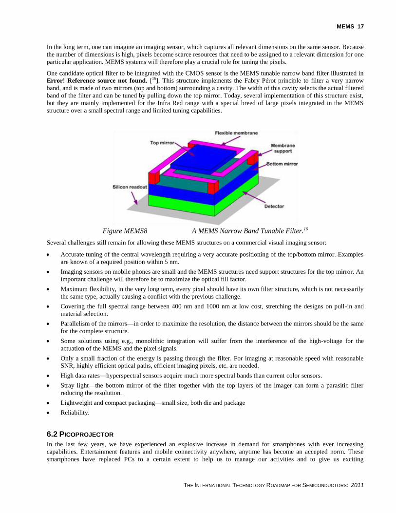
In the long term, one can imagine an imaging sensor, which captures all relevant dimensions on the same sensor. Because
the number of dimensions is high, pixels become scarce resources that need to be assigned to a relevant dimension for one
particular application. MEMS systems will therefore play a crucial role for tuning the pixels.
One candidate optical filter to be integrated with the CMOS sensor is the MEMS tunable narrow band filter illustrated in
Error! Reference source not found. [16
]. This structure implements the Fabry Pérot principle to filter a very narrow
band, and is made of two mirrors (top and bottom) surrounding a cavity. The width of this cavity selects the actual filtered
band of the filter and can be tuned by pulling down the top mirror. Today, several implementation of this structure exist,
but they are mainly implemented for the Infra Red range with a special breed of large pixels integrated in the MEMS
structure over a small spectral range and limited tuning capabilities.
Figure MEMS8 A MEMS Narrow Band Tunable Filter.16
Several challenges still remain for allowing these MEMS structures on a commercial visual imaging sensor:
Accurate tuning of the central wavelength requiring a very accurate positioning of the top/bottom mirror. Examples
are known of a required position within 5 nm.
Imaging sensors on mobile phones are small and the MEMS structures need support structures for the top mirror. An
important challenge will therefore be to maximize the optical fill factor.
Maximum flexibility, in the very long term, every pixel should have its own filter structure, which is not necessarily
the same type, actually causing a conflict with the previous challenge.
Covering the full spectral range between 400 nm and 1000 nm at low cost, stretching the designs on pull-in and
material selection.
Parallelism of the mirrors—in order to maximize the resolution, the distance between the mirrors should be the same
for the complete structure.
Some solutions using e.g., monolithic integration will suffer from the interference of the high-voltage for the
actuation of the MEMS and the pixel signals.
Only a small fraction of the energy is passing through the filter. For imaging at reasonable speed with reasonable
SNR, highly efficient optical paths, efficient imaging pixels, etc. are needed.
High data rates—hyperspectral sensors acquire much more spectral bands than current color sensors.
Stray light—the bottom mirror of the filter together with the top layers of the imager can form a parasitic filter
reducing the resolution.
Lightweight and compact packaging—small size, both die and package
Reliability.
6.2 PICOPROJECTOR
In the last few years, we have experienced an explosive increase in demand for smartphones with ever increasing
capabilities. Entertainment features and mobile connectivity anywhere, anytime has become an accepted norm. These
smartphones have replaced PCs to a certain extent to help us to manage our activities and to give us exciting
18 MEMS
THE INTERNATIONAL TECHNOLOGY ROADMAP FOR SEMICONDUCTORS: 2011
entertainment and ubiquitous social interaction. Picoprojectors can play a major role in this development as they can
visualize the persons we are interacting with, beam a video, photo or presentation from your phone onto a wall or screen
to view it full-size and share with others. Video is indeed an inherently social experience that people want to share. In the
future picoprojectors might also create virtual reality for the games we play.
Three years ago when TI unveiled its tiny picoprojectors for mobile devices, device makers quickly built pico-projectors
into digital still cameras, camcorders, media players and docking stations. Cellphone manufacturers were, however,
slower on the uptake. Fujitsu and Sharp have already released handsets with picoprojectors. Samsung has recently
followed suit. But development fizzled and picoprojectors looked like a short-lived gadget. However, according to
industry pioneer TI, technology trends such as the upgrade to faster, 4G cellular networks and the move to tiered pricing
for wireless data have made picoprojector phones newly relevant. The company believes projectors will become as
ubiquitous in phones as in cameras, pointing to analyst projections that anticipate tens of millions of pico-enabled devices
by 2013. DLP sales have been growing 300% a year across the various mobile device categories and now span more than
20 brands and 30 types of products [17
]. Not only TI sees a bright future for picoprojectors. Mark Fihn (publisher of the
Veritas et Visus newsletters) predicts that—although some hurdles still exist—picoprojectors are winning the race to
enable big images from small packages. Rollable or foldable displays are clearly on the losing side [18
].
Present day pico-projectors in handheld tools are mostly based on low-resolution 2D imagers such as the 480x320 pixels
DLP chips from TI, shown in Error! Reference source not found. [19
].Higher resolutions are a challenge due to size
limitations and small-pixel induced diffraction effects. Competing technologies that try to overcome this resolution
limitation comprise scanning-mirror projectors (Bitendo, Pixtronix) and the more recent diffractive grating and
holographic projection solutions (Light Blue Optics, Silicon Light Machines). Scanning mirror picoprojectors are small
enough to be integrated inside mobile phones, but no such integrated products are commercially available today.
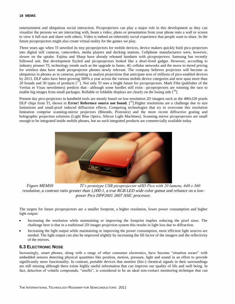
Figure MEMS9 TI’s prototype USB picoprojector nHD Pico with 20 lumens, 640 x 360
resolution, a contrast ratio greater than 1,000:1, a true RGB LED wide color gamut and reliance on a low-
power Pico DPP2601 2607 ASIC processor.
The targets for future picoprojectors are a smaller footprint, a higher resolution, lower power consumption and higher
light output:
Increasing the resolution while maintaining or improving the footprint implies reducing the pixel sizes. The
challenge here is that in a traditional 2D imager projection system this results in light loss due to diffraction.
Increasing the light output while maintaining or improving the power consumption, more efficient light sources are
needed. The light output can also be improved slightly by increasing the fill factor of the imagers and the reflectivity
of the mirrors.
6.3 ELECTRONIC NOSE
Increasingly, smart phones, along with a range of other consumer electronics, have become “situation aware” with
embedded sensors detecting physical quantities like position, motion, pressure, light and sound in an effort to provide
significantly more functionality. In contrast, portable devices that monitor (bio-) chemical signals in their surroundings
are still missing although there exists highly useful information that can improve our quality of life and well being. In
fact, detection of volatile compounds, “smells”, is considered to be an ideal non-contact monitoring technique that can

MEMS 19
THE INTERNATIONAL TECHNOLOGY ROADMAP FOR SEMICONDUCTORS: 2011
provide insight into chemical as well as biological interactions that often result in emission of volatile organic
compounds. However, in many cases, the target “smell” is a complex mixture of volatile compounds and analytical tools
like spectrometers that can precisely identify them are not scalable nor sufficiently power efficient for integrated
solutions. An alternative approach is the use of partially selective sensing elements for fingerprinting of volatile mixtures
in systems referred to as “electronic nose”, due to their resemblance to the mammalian olfaction mechanism. Electronic
noses, or e-noses, are already deployed in a range of tasks ranging from quality control to safety and security. However,
there exists a range of applications that current e-nose technologies are unable to target due to their size and power
consumption. Personal breath analyzers, either for preliminary diagnosis or monitoring of conditions for medication
dosing, would be of considerable value to patients with chronic health problems like asthma. Air quality monitors in
smart phones could potentially warn individual users to stay away from environments that can specifically harm them due
to their existing medical conditions. As such, there is a growing demand in scalable, arrayable, integrated and low power
sensing elements that can be customized for detection of chemicals in specific application conditions.
Table MEMS7 summarizes several arrayable sensor technologies that have been developed over recent years for
electronic nose systems, albeit with individual challenges and limitations. Clearly, these solutions are not fulfilling the
requirements of integrating a miniaturized electronic nose into portable consumer electronics. Increasingly, MEMS-based
detection solutions are emerging as potential solutions to the above-described limitations in chemical sensors. Cantilevers,
from atomic force microscope technology, have been adapted by polymer functionalization in both static and dynamic
(resonant) mode operation [20
,21
]. An inertial sensing scheme developed in quartz crystals has also been revisited in
various integrated microfabricated structures. In one of the most promising approaches, capacitive MEMS membranes
coated with polymers were demonstrated to achieve sub-ppm sensitivity [22
]. Here, the reproducibility of MEMS
fabrication techniques and scalability advantages were leveraged to construct very large arrays of resonators with
identical coatings that were connected in parallel in an effort to improve effective circuit characteristics, albeit at a cost of
total size and power consumption [23
].
Alternatively, MEMS in-plane disk resonators have been developed with thermal excitation in an effort to overcome the
squeeze film fluidic damping effects but resulting in considerably higher power consumption [24
]. To overcome the
restrictions in limit of detection for low-molecular weight analytes using the above described gravimetric schemes, an
alternative approach based on a stress-induced resonance frequency change was developed where low-power consuming
microbridge piezoelectric resonators were coated with polymers that demonstrate a volumetric response to analyte
absorption [25
].
As more e-nose technologies are maturing towards embedment in mobile applications, the performance metrics for these
need to be clarified. Foremost, small form factor and low power consumption are the main requirements, with 1 cm2
device size and sub-mW operation, including the read-out circuitry, being considered current benchmarks for a multi-
receptor array of sensing elements. These specifications clearly require a significant amount of system level optimization
for the sensor node. The complexity of the system, containing chemistry, (electromechanical) transduction and electronic
read-out, rapidly turns the optimization task into a challenging interdisciplinary activity. Furthermore, complexities of the
chemical interactions with the transducer often result in lack of deterministic models of the sensing elements. As such, a
significant amount of experimental results need to be accumulated in an effort to gain in-depth understanding of the
system. This requires well-established and robust measurement procedures that can be applied for testing under various
chemical conditions.
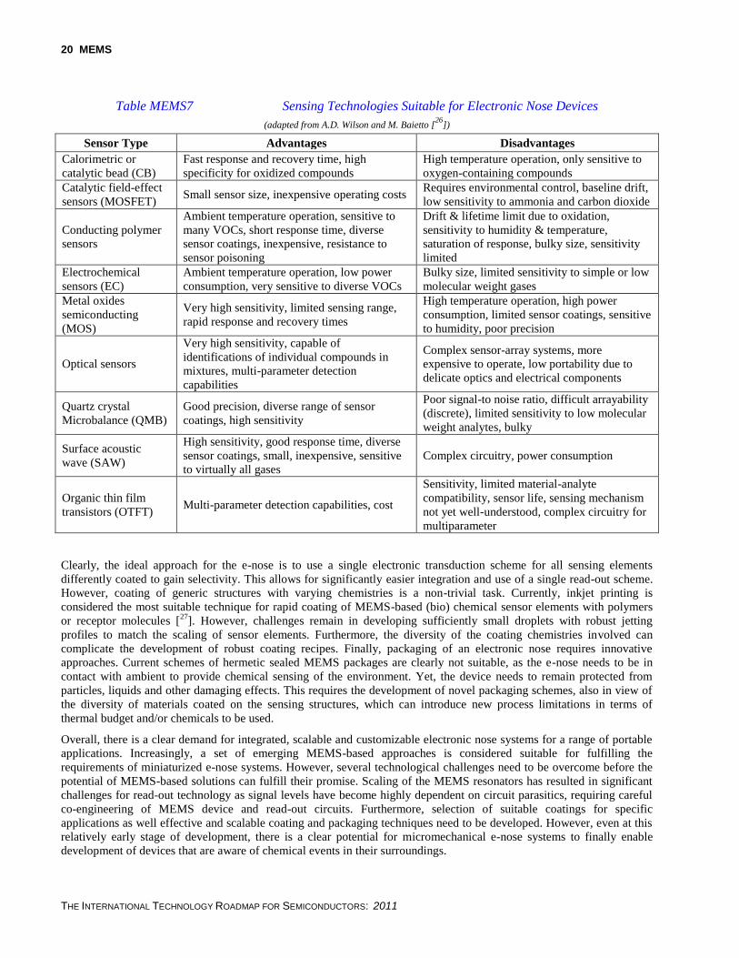
20 MEMS
THE INTERNATIONAL TECHNOLOGY ROADMAP FOR SEMICONDUCTORS: 2011
Table MEMS7 Sensing Technologies Suitable for Electronic Nose Devices
(adapted from A.D. Wilson and M. Baietto [26
])
Sensor Type Advantages Disadvantages
Calorimetric or
catalytic bead (CB)
Fast response and recovery time, high
specificity for oxidized compounds
High temperature operation, only sensitive to
oxygen-containing compounds
Catalytic field-effect
sensors (MOSFET) Small sensor size, inexpensive operating costs
Requires environmental control, baseline drift,
low sensitivity to ammonia and carbon dioxide
Conducting polymer
sensors
Ambient temperature operation, sensitive to
many VOCs, short response time, diverse
sensor coatings, inexpensive, resistance to
sensor poisoning
Drift & lifetime limit due to oxidation,
sensitivity to humidity & temperature,
saturation of response, bulky size, sensitivity
limited
Electrochemical
sensors (EC)
Ambient temperature operation, low power
consumption, very sensitive to diverse VOCs
Bulky size, limited sensitivity to simple or low
molecular weight gases
Metal oxides
semiconducting
(MOS)
Very high sensitivity, limited sensing range,
rapid response and recovery times
High temperature operation, high power
consumption, limited sensor coatings, sensitive
to humidity, poor precision
Optical sensors
Very high sensitivity, capable of
identifications of individual compounds in
mixtures, multi-parameter detection
capabilities
Complex sensor-array systems, more
expensive to operate, low portability due to
delicate optics and electrical components
Quartz crystal
Microbalance (QMB)
Good precision, diverse range of sensor
coatings, high sensitivity
Poor signal-to noise ratio, difficult arrayability
(discrete), limited sensitivity to low molecular
weight analytes, bulky
Surface acoustic
wave (SAW)
High sensitivity, good response time, diverse
sensor coatings, small, inexpensive, sensitive
to virtually all gases
Complex circuitry, power consumption
Organic thin film
transistors (OTFT) Multi-parameter detection capabilities, cost
Sensitivity, limited material-analyte
compatibility, sensor life, sensing mechanism
not yet well-understood, complex circuitry for
multiparameter
Clearly, the ideal approach for the e-nose is to use a single electronic transduction scheme for all sensing elements
differently coated to gain selectivity. This allows for significantly easier integration and use of a single read-out scheme.
However, coating of generic structures with varying chemistries is a non-trivial task. Currently, inkjet printing is
considered the most suitable technique for rapid coating of MEMS-based (bio) chemical sensor elements with polymers
or receptor molecules [27
]. However, challenges remain in developing sufficiently small droplets with robust jetting
profiles to match the scaling of sensor elements. Furthermore, the diversity of the coating chemistries involved can
complicate the development of robust coating recipes. Finally, packaging of an electronic nose requires innovative
approaches. Current schemes of hermetic sealed MEMS packages are clearly not suitable, as the e-nose needs to be in
contact with ambient to provide chemical sensing of the environment. Yet, the device needs to remain protected from
particles, liquids and other damaging effects. This requires the development of novel packaging schemes, also in view of
the diversity of materials coated on the sensing structures, which can introduce new process limitations in terms of
thermal budget and/or chemicals to be used.
Overall, there is a clear demand for integrated, scalable and customizable electronic nose systems for a range of portable
applications. Increasingly, a set of emerging MEMS-based approaches is considered suitable for fulfilling the
requirements of miniaturized e-nose systems. However, several technological challenges need to be overcome before the
potential of MEMS-based solutions can fulfill their promise. Scaling of the MEMS resonators has resulted in significant
challenges for read-out technology as signal levels have become highly dependent on circuit parasitics, requiring careful
co-engineering of MEMS device and read-out circuits. Furthermore, selection of suitable coatings for specific
applications as well effective and scalable coating and packaging techniques need to be developed. However, even at this
relatively early stage of development, there is a clear potential for micromechanical e-nose systems to finally enable
development of devices that are aware of chemical events in their surroundings.
MEMS 21
THE INTERNATIONAL TECHNOLOGY ROADMAP FOR SEMICONDUCTORS: 2011
6.4 MICROSPEAKERS
Smart phone manufacturers (along with other consumer product manufacturers) have been early adopters of MEMS-
based sensors used for detecting physical (and chemical) input signals in an attempt to create more “situation awareness”
and to provide more functionality per unit volume (or unit area). The most common ones are position, motion, pressure
(altitude measurement), temperature, magnetic field (electronic compass), humidity, light (image) and not to forget, audio
sound (microphone). In contrast, MEMS-based actuators, like RF switching devices, projectors for light and audio
acoustic actuators (loudspeakers), are still (for a great part) missing.
Evidently, audio acoustic transducer elements (microphones and speakers) are essential and indispensable components in
a smart phone. “Size matters” and electronics manufacturers are prompting the miniaturization of acoustic elements.
MEMS technology clearly offers a viable route to achieve this miniaturization, while at the same time offering multiple
components and on-chip signal processing. MEMS-based microphones have already seen adoption into the mobile phone
market since 2006, opening the door to similar opportunities for sound generation using MEMS-based micro speakers.
Loudspeakers for smart phones however, are nowadays still build using conventional techniques relying on precision
mechanics. Regal Electronics, for example, has added a new product that is close to 15mm in diameter yet can handle up
to a watt of peak input power. The new speaker (constructed with a metal frame and Mylar diaphragm) has a frequency
range of 600Hz to 20kHz. Although this is clearly a step forward, the mini speaker is still quite large (and thick) and
moreover it is not compatible with automated assembly equipment, something that should improve manufacturing
throughput and yield and potentially lead to a lower cost.
Today, commercially available MEMS-based micro speakers have not been identified. However, there are reports in the
scientific and patent literature for fabrication techniques and generating sound using on-chip micro speakers and micro
speaker arrays [1-5]. The targets and challenges for future micro loudspeakers for use in smart phones/tablets are a small
footprint, low (flat) profile, small weight, extended frequency range (a high fidelity sound), low voltage actuation, high
efficiency (low power consumption), sufficient sound output power, standard assembly and low cost.
MEMS-based micromachined membrane type actuators can be used to generate sound in the audio frequency range. One
challenge to overcome is how to achieve sufficient output pressure at a relatively low actuation (bias) voltage. For the
commonly employed electrostatic drive [28
], the (bias) voltage is quite high, e.g., on the order of 40-70Vdc. Changing to
other actuation means like piezoelectric [29
,30
] or electrodynamic [31
] (as used in traditional moving-coil loudspeakers)
presents a potential solution, but this may come at higher complexity (e.g., integration of piezoelectric materials or
integration of a permanent magnet) and/or higher current and thus higher power consumption and lower power efficiency
(for the electrodynamic).
A more fundamental challenge for membrane speaker actuators is how to achieve significant sound pressures with a
device of small area. Speakers generate sound by moving air. Moving large volumes of air is achieved using large area
membranes and/or inducing large membrane displacements. In particular for the low frequencies this becomes
problematic as the radiation impedance (which determines the pressure generated for a given membrane displacement)
decreases with decreasing frequency. In particular, this is true for radiation in free air as opposed to for instance ear
phones which are confronted with a smaller challenge as the small volume of the ear canal presents a larger acoustic
impedance than is achievable in free air [28
]. Relaxing therefore on the frequency response spec (especially into the low
frequencies, e.g., <600Hz) opens the way to analog MEMS-based loudspeakers.
One possible route to take in order to overcome the above “radiation” challenge is to deviate from the conventional
analog speakers and to go digital. It is noted that modern speakers marketed as 'digital' are always analog speakers, in
most cases driven by an analog amplifier. The use of the term 'digital' for speakers is a marketing strategy intended to
claim better suitability with 'digital' source material (e.g., MP3 recordings). True digital speakers rely on direct conversion
of electrical input to sound, thereby eliminating the need for a digital-to-analog converter accounting for the incongruity
between the analog speaker and the digital electronics used for the necessary signal processing [32
,33
]. More specifically,
the concept of “digital sound reconstruction (DSR)” is enabled by the collective action of hundreds to thousands of
individual and identical binary (membrane-type) speaker elements (an alternative approach employs a single speaker and
uses some fraction of the speaker's actuator to define the bits). Unlike analog speakers where the frequency response is
one of the primary characteristics, for digital speakers, it is a fast pulse response of the individual speaker elements that is
required.
It all comes down to achieving a microspeaker system that is optimized for quality of the sound and output power for the
size, weight, complexity, and cost.

22 MEMS
THE INTERNATIONAL TECHNOLOGY ROADMAP FOR SEMICONDUCTORS: 2011
6.5 ULTRASOUND DEVICES
Ultrasounds are sound waves typically defined as having frequencies above 20kHz. Like all sound waves, they propagate
in elastic solid, in gaseous or in liquid materials. Ultrasounds propagate for example well in silicon, air and water where
they present thus wavelengths smaller than 40cm, 2cm and 8cm respectively. In comparison, electromagnetic waves do
not require any supporting medium for their propagation, present above 20kHz in vacuum wavelengths smaller than
15km, require in vacuum frequencies in excess of 30GHz to reach wavelengths of 1cm. Further, electromagnetic waves
typically propagate poorly in water and silicon.
Ultrasound applications are numerous and varied; from positioning/ranging to medical treatment, through actuation,
levitation, and drug delivery. Among these, telecom, non-destructive testing and imaging applications lead the
developments of game-changer ultrasound devices. Indeed, emerging micromachined devices are challenging the
dominancy of current piezoelectric ultrasound transducers. Micromachined ultrasound transducers (MUTs) typically
consist of free-standing membranes and a mean to actuate/sense these, e.g., c(apacitive)MUTs – electrostatics,
p(iezoelectric)MUTs - piezoelectrics. Among these, cMUTs are the most widely known, studied and developed. See
Figure 10.
The development of MUTs is fueled by several trends that in particular apply to the medical imaging applications and
businesses:
Ultrasound systems made cheap—MUTs can be highly integrated, mass-fabricated with high accuracy in dense
arrays in CMOS foundries.
Ultrasound systems made portable—MUTS will fuel the booming market of portable ultrasound imaging systems by
their low price and ease of integration. They will enable tele-monitoring of patients, broaden the range of available
wellness applications and allow monitoring devices to reach patients at most diverse points of care.
Ultrasound systems made wearable—The simplified MUT-based systems can be incorporated in conformal and
stretchable medical patches for continuous ambulatory cardiosonography.
High end ultrasound systems—MUTs can be tightly integrated, in densely packed large arrays, with their drive and
readout electronics, lowering the parasitics and increasing thus the realized SNRs (signal to noise ratio). MUTs are
key enablers for 4D (volumetric-temporal) imaging systems with large channel-counts.
Ultrasound systems made flexible—a key feature of MUTs is their ability to produce ultrasound in wide bandwidths
and to extend their working frequencies easily above the 10MHz frequency range. This translates in high-fidelity
multipurpose ultrasound imaging systems.
Ultrasound systems made rugged—Integrated with their analog ICs, MUTs bring the digital layers of imaging
systems closer to the transducers themselves. With purely digital outputs, the resulting compact probe-heads have
simple and robust interfaces to the image processing units.
(a) (b) (c)
Figure MEMS10 (a) Schematic cross-section of a capacitive micromachined
ultrasound transducer (cMUT), (b) SEM detail of four dual thickness cMUT cells from a 2D array of
acoustic pixels, and (c) COMSOL simulation of the first eigenmode of a dual thickness cMUT cell.
MEMS 23
THE INTERNATIONAL TECHNOLOGY ROADMAP FOR SEMICONDUCTORS: 2011
Key technical challenges for MUTs include:
Improvement in reliability.
Packaging and integration schemes, including high-density TSVs and 3D-stacking techniques.
Design environments for MUT-based systems.
Cost reduction.
Performance validation and certification for specific medical applications.
7 CONCLUSIONS The back-end of MEMS manufacturing (packaging and testing) consumes ⅔ of the total manufacturing cost [
34] yet
virtually all R&D investment has been in the front-end of manufacturing (devices and process development), which can
be attributed to a lack of articulation of the problems and their importance. The roadmapping efforts described in this
report are the first steps in the long journey of communicating the industrial needs for MEMS technology to advance
along its projected technology timeline. The development of a consensus opinion that documents the issues facing the
industry, which is the primary output from technology roadmapping, can be used as a tool to optimize R&D investment
that meets critical manufacturing needs in a timely manner.
This roadmap considered both the evolution of discrete MEMS devices and integrated MEMS technologies. This term
“discrete” MEMS is used to refer to devices that perform one function. For example, a 3-axis accelerometer with an
integrated ASIC is referred to as a discrete MEMS device for the purposes of this discussion. Integrated MEMS, also
referred to as multimode sensors, refers to the integration of sensing functions, such as accelerometer and gyroscope, in
the same package.
Discrete MEMS devices are expected to see a continuous incremental increase in performance, and reduction in cost and
package size. The greatest challenges for them are related to packaging: decreasing package size while at the same time
drastically lowering cost. There are no known solutions to meet the packaging and cost projections out to 2017.
The MEMS TWG sees the greatest challenges for MEMS technologies are in relation to their integration path. The
integration path towards the Inertial Measurement Unit (IMU) is to join 3-axis accelerometers, 3-axis gyroscopes, 3-axis
magnetometers (compass), and a pressure sensor (altimeter). This is referred to as a 10 degree of freedom (DOF)
multimode sensor. The TWG focused its attention on the accelerometers and gyroscopes, however, future iterations of the
roadmap should include magnetometers and pressure sensors. Pressure sensors are MEMS devices that will be integrated
in the future IMUs used in mobile devices. Though magnetometers are not, by definition, MEMS devices, they are
inclusive to the More-than-Moore paradigm.
Multimode sensor technologies face challenges in assembly and packaging, especially for integration of the IMU at the
package level, yet these are challenges where interim solutions are known. The greatest concern for multimode sensor
technologies, with no known solutions, relates to testing. Possible solutions discussed in this report relate to moving as
much of the testing as possible to earlier steps in the manufacturing process, such as wafer-level tests. This will require
the ability to accurately predict performance at the package-level from the wafer-level tests. Other solutions include
advancing know-how for MEMS design for testability and even to develop ways to eliminate testing, referred to as to
“design for no test.”
There is a continuing need to extend knowledge of the physics of failure in MEMS. This is especially relevant for RF
MEMS devices, where their adoption in many applications has been hindered. Extending knowledge of the physics of
failure will enable how to improve their reliability and for developing reliability accelerated test methods. It is recognized
that there is knowledge for specific devices that resides with companies; however, this knowledge has traditionally been
kept secret because it results in commercial advantage. Sharing information may become beneficial at an appropriate
time.
The MEMS TWG examined the near-term technology requirements for the MEMS technologies in this roadmap. While
there is a desire to expand discussions to include the long-term, the committee must first reach a consensus on how this
will be done for MEMS technologies. It may be that long-term requirements for MEMS may concern integration path,
e.g., integration with multiple sensor technologies, advancing ASIC requirements to microcontroller, package level
integration versus 3D staking technologies versus monolithic integration paths. Thus near-term requirements may concern
incremental advances in device performance metrics within integration cycles of integration over the long-term.

24 MEMS
THE INTERNATIONAL TECHNOLOGY ROADMAP FOR SEMICONDUCTORS: 2011
Roadmapping integration path over the long term will require accurate cost analysis, ensuring that future predictions of
the price of a MEMS component are consistent with the resources and technology needed to deliver to the market place.
Currently, the methodology can be usefully employed to cost/price discrete MEMS devices and predict the production
developments needed for the immediate future. Accurately costing future integrated MEMS devices represents a
significant challenge, particularly in estimating the structure of costs to solve the technical problems in integrating
fundamentally different components, the cost of developing cost-effective test equipment and the formidable task of
packaging in large scale manufacture.

MEMS 25
THE INTERNATIONAL TECHNOLOGY ROADMAP FOR SEMICONDUCTORS: 2011
8 REFERENCES
[1] http://www.inemi.org/2011-inemi-roadmap
[2] R. P. Feynman, There’s Plenty of Room at the Bottom, JMEMS, vol. 1, no. 1, p. 66, March 1992. Reprinted in
JMEMS with the consent of Van Nostrand Reinhold, New York, NY, 10003.
[3] O. N. Tufte, et al., Silicon diffused-element piezoresistive diaphragms, Journal of Applied Physics, 33, 1962.
[4] R. Howe and R. S. Muller R.S, Polycristalline silicon micromachined beams, Jour. Electrochem. Soc., 130, 1420-
1423, 1983.
[5] S. Walsh and J. Elders, (Eds.), International Roadmap on MEMS, Microsystems, Micromachining and Top Down
Nanotechnology, MANCEF, Naples, Florida, 2003, printed in Germany and the United States.
[6] G. E. Moore, Cramming more components onto integrated circuits, Electronics, Volume 38, Number 8, April 19,
1965.
[7] R. R. Tummala, Moore's Law Meets Its Match, IEEE Spectrum, p. 44, June 2006.
[8] ITRS More-than-Moore White Paper, http://www.itrs.net/papers.html.
[9] iNEMI Technology Roadmap, January 2011.
[10
] P. Walter, The History of the Accelerometer, Sound and Vibration, p. 84, January 2007.
[11
] L. M. Roylance and J. B. Angell, A Batch-Fabricated Silicon Accelerometer, IEEE Trans. Elec. Dev., ED-26, 1911
(1979).
[12
] J. V. Clark, “Electro micro-metrology,” Ph.D. dissertation, Dept. Appl. Sci. Technol., Univ. California, Berkeley,
CA, 2005.
[13
] S.K. Nayar, "Computational Cameras: Redefining the Image", IEEE Computer Magazine, Special Issue on
Computational Photography, pp.30-38, Aug, 2006.
[14
] P. B. Catrysse and B.A. Wandell, “Integrated color pixels in 0.18-µm complementary metal oxide semiconductor
technology,” J. Opt. Soc. Am. A, Vol. 20, No. 12, pages 2293-2306.
[15
] N. Gupta, P. R. Ashe and S. Tan, “Miniature snapshot multispectral sensor”,Optical engineering, Vol. 50, No. 3,
2011.
[16
] L Faraone, J Dell, and C Musca, Micro/Nano Lithography, “Infrared micro-spectrometers for low-cost, portable
applications,” SPIE Newsroom.
[17
] http://blogs.forbes.com/elizabethwoyke/2011/04/26/ti-says-pico-projectors-poised-for-mobile-phone-resurgence/
[18
] Information Display 5/11 “Predicting the Future.”
[19
] http://www.crunchgear.com/wp-content/uploads/2011/02/dlp-02.jpg, http://www.engadget.com/2011/02/15/texas-
instruments-shows-off-minuscule-nhd-pico-projector-chipset/
[20
] H.P. Lang, M.K. Baller, R. Berger, and C. Gerber, “An artificial nose based on a micromechanical cantilever array,”
Analytica Chimica, vol. 393, Jun. 1999, pp. 59-65.
[21
] M. Baller, H. Lang, J. Fritz, C. Gerber, J. Gimzewski, U. Drechsler, H. Rothuizen, M. Despont, P. Vettiger, F.
Battiston, J. Ramseyer, P. Fornaro, E. Meyer, and H.-J. Guntherodt, “A cantilever array-based artificial nose,”
Ultramicroscopy, vol. 82, 2000, pp. 1-9.
[22
] K. Park, H. Lee, G. Yaralioglu, A. Ergun, O. Oralkan, M. Kupnik, C. Quate, B. Khuri-Yakub, T. Braun, J.-P.
Ramseyer, H. Lang, M. Hegner, C. Gerber, and J.K. Gimzewski, “Capacitive micromachined ultrasonic transducers
for chemical detection in nitrogen,” Applied Physics Letters, vol. 91, 2007, p. 094102–094102.
[23
] H.J. Lee, K.K. Park, P. Cristman, O. Oralkan, M. Kupnik, and B.T. Khuri-Yakub, “A Low-Noise Oscillator based
on a Multi-Membrane CMUT for High Sensitivity Resonant Chemical Sensors,” IEEE 22nd International
Conference on Micro Electro Mechanical Systems (MEMS), 2009, pp. 761-764.
[24
] S.B. Truax, K.S. Demirci, L. a Beardslee, Y. Luzinova, A. Hierlemann, B. Mizaikoff, and O. Brand, “Mass-
sensitive detection of gas-phase volatile organics using disk microresonators.,” Analytical chemistry, vol. 83, May.
2011, pp. 3305-11.
26 MEMS
THE INTERNATIONAL TECHNOLOGY ROADMAP FOR SEMICONDUCTORS: 2011
[25
] S.B. Truax, K.S. Demirci, L. a Beardslee, Y. Luzinova, A. Hierlemann, B. Mizaikoff, and O. Brand, “Mass-
sensitive detection of gas-phase volatile organics using disk microresonators.,” Analytical chemistry, vol. 83, May.
2011, pp. 3305-11.
[26
] A.D. Wilson and M. Baietto, “Applications and advances in electronic-nose technologies,” Sensors, vol. 9, 2009, p.
5099–5148.
[27
] A. Bietsch, J. Zhang, M. Hegner, and H.P. Lang, “Rapid functionalization of cantilever array sensors by inkjet
printing,” Nanotechnology, vol. 15, 2004, pp. 873-880.
[28
] J. J. Neumann, Jr. and K. J. Gabriel, "CMOS-MEMS membrane for audio-frequency acoustic actuation", in
Technical Digest of the 14th IEEE International Conference on Micro Electro Mechanical Systems (MEMS '01),
January 2001, Interlaken, Switzerland, pp. 236-239, 2001.
[29
] C. H. Han and E. S. Kim, “Parylene-Diaphragm Piezoelectric Acoustic Transducers”, in Technical Digest of the
13th IEEE International Conference on Micro Electro Mechanical Systems (MEMS 2000), Miyazaki, Japan, pp.
148-152, 2000.
[30
] S. S. Lee, R. P. Reid and R. M. White, “Piezoelectric cantilever microphone and microspeaker”, J. of
Microelectromechanical Systems, vol. 5(4), pp. 238-242, Dec. 1996.
[31
] S.-S. Je, F. Rivas, R. E. Diaz, J. Kwon, J. Kim, B. Bakkaloglu, S. Kiaei, Fellow and J. Chae, “A compact and low-
cost MEMS loudspeaker for digital hearing aids”, IEEE Trans. On Biomedical Circuits and Systems, vol. 3(5), pp.
348-358, Oct. 2009.
[32
] B.M. Diamond, J. J. Neumann and K. J. Gabriel, “Digital Sound Reconstruction Using Arrays of CMOS-MEMS
Microspeakers”, in Technical Digest of the 12th International Conference on Solid State Sensors, Actuators and
Microsystems (Transducers’03), Boston, June 8-12, 2003, pp. 238-241, 2003.
[33
] J. L. Flanagan, “Direct digital-to-analog conversion of acoustic signals”, The Bell System Technical Journal, vol.
59(9), pp. 1693-1719, 1980.
[34
] MEMS Testing Standards: A Path to Continued Innovation, Workshop Report on MEMS Testing Standards
Workshop, MEMS Industry Group, San Jose, CA, March 15 - 16, 2011.