Embed Size (px)
Citation preview
LV MFM™
Filter
Low Voltage MIL-COTS Input Filter Module
MFM1714x50M50C5yzz
LV MFM™ Filter Rev 1.1Page 1 of 16 07/2017
Features & Benefits
• 28V Nominal input
• 99% efficiency
• EMI filtering
MIL-STD-461E/F, selected CE and CS tests
• Input Transient protection
MIL-STD-1275A/B/D/E
MIL-STD-704A/F (MIL-HDBK-704-8) Normal and Abnormal Transients
• Envronmental qualification
MIL-STD-810
MIL-STD-202
• Low M grade temperature rating, providing operation down to -55°C
• Output power up to 350W
• Available in chassis and PCB mount
• Small size
1.76” x 1.40” x 0.36” (44.6mm x 35.5mm x 9.2mm)
Typical Applications
• Defense
• Aerospace
Compatible Products
• Low input voltage DCM in a VIA Package
• Low input voltage ChiP [1] DCM
Product Description
The MFM DCM Filter is a DC front-end module that provides EMI filtering and transient protection. The MFM DCM Filter enables designers using Vicor’s 28V nominal input voltage VIA or ChiP [1] modules to meet conducted emission/conducted susceptibility per MIL-STD-461E/F; and input transients per MIL-STD-704A/F, MIL-STD-1275A/B/D/E and DO-160E. The MFM DCM Filter accepts an input voltage of 16 – 50VDC (28V nominal input ) and delivers output power up to 350W.
Size:1.76 x 1.40 x 0.36in44.6 x 35.5 x 9.2mm
Part Ordering Information
ProductFunction
Package Length
PackageWidth
PackageType
MaxHighSide
Voltage
High Side
VoltageRangeRatio
Max LowSide
Voltage
MaxLowSide
Current
ProductGrade(Case
Temperature)
Option Field
MFM 17 14 x 50 M 50 C5 y zz
MFM =MIL-COTS Input
Filter Module
Length in Inches x 10
Width in Inches x 10
B = Board VIAV = Chassis VIA
Internal Reference M = -55 to 100°C00 = Chassis
04 = Short Pin08 = Long Pin
[1] Additional components are required for EMI filtering and transient suppression, when used with ChiP modules.
LV MFM™ Filter Rev 1.1Page 2 of 16 07/2017
MFM1714x50M50C5yzz
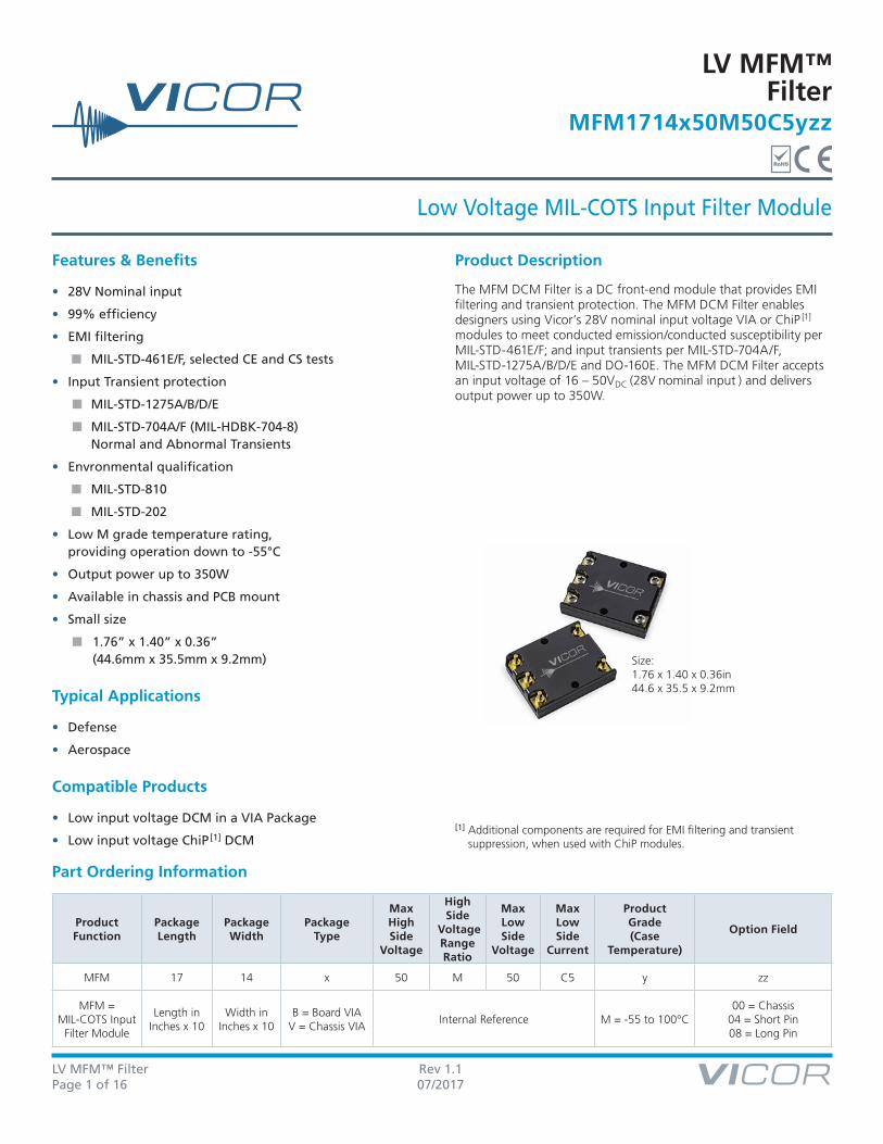
16 - 50VSource
VDDE
EN TR
-SENSE +SENSE
LOAD
MFM+IN +OUT
EMI GND
-IN
+IN
-IN -OUT
+OUT
-OUT
earth ground
DCMTM in a VIA package
CINCIN-DCM COUT-EXT
F
M-Grade DCM in a VIA package with a MFM input filter, to meet the EMI and transient requirements
Typical Application
Parts List for Typical Applications
FEATON (Cooper/Bussman) ABC series, fast acting tube fuses rated 30A
Littlefuse NANO2 456 Series, surface mount fuses rated 30A

LV MFM™ Filter Rev 1.1Page 3 of 16 07/2017
MFM1714x50M50C5yzz
MFM Filter in a VIA Package - Chassis (Lug) Mount - Terminals Up
MFM Filter in a VIA Package - PCB Mount - Pins Down
+IN
-IN
+OUT
-OUT
EMIGND
-IN
+IN
-OUT
+OUT
EMIGND
Pin Configuration
Pin Descriptions
Signal Name Type Function
+IN INPUT POWER Positive input power terminal
–ININPUT POWER
RETURNNegative input power terminal
EMI GND EMI GROUND EMI ground terminal
+OUT OUTPUT POWER Positive output power terminal
–OUTOUTPUT POWER
RETURNNegative output power terminal
Note: These Pin drawings are not to scale.

LV MFM™ Filter Rev 1.1Page 4 of 16 07/2017
MFM1714x50M50C5yzz
Absolute Maximum Ratings
The absolute maximum ratings below are stress ratings only. Operation at or beyond these maximum ratings can cause permanent damage to the device. Electrical specifications do not apply when operating beyond rated operating conditions.
Parameter Comments Min Max Unit
Input Voltage (+IN to –IN)
Continuous -0.5 65.0
VDC
Transient per MIL-STD-1275D/E, 50ms 100
Transient per MIL-STD-1275A/B/D, 70µs 250
Transient per DO-160E, 100ms 80
Output Voltage (+OUT to –OUT) -0.5 65.0 VDC
Dielectric Withstand (Input/Output to EMI GND/Case)
1500 VDC
Storage Temperature M-Grade -65 125 °C
Internal Operating Temperature M-Grade -55 125 °C
Average Output Current 22 A
Input/Output Pin Torque and Mounting Torque
4 (0.45) in-lbs (N-m)
Electrical Specifications
Specifications apply over all line and load conditions, unless otherwise noted; boldface specifications apply over the temperature range of -55°C ≤ TCASE ≤100°C (M-Grade); all other specifications are at TCASE = 25ºC unless otherwise noted.
Attribute Symbol Conditions / Notes Min Typ Max Unit
Power Input / Output Specification
Input Voltage Range [2] VIN
Continuous operation 16 28 50
VTransient per MIL-STD-1275D/E, 50ms 100
Transient per MIL-STD-1275A/B/D, 70µs 250
Transient per DO-160E, 100ms 80
Maximum Output Current [3] IOUT_MAXContinuous, at VOUT = 16V (IOUT = POUT/VIN)
22 A
Rated Output Power [3] POUT Continuous, over all line conditions 350 W
Internal Voltage Drop @16V, 22A, 100°C baseplate 0.65 VDC
Efficiency η
Full load, low line, high temperature 97.7 98 98.2 %
Full load, nominal line, high temperature 99.2 99.4 %
Full load, high line, high temperature 99.7 99.8 %
[2] Transient immunity specifications are met only when LV MFM is used with M-grade 16-50VIN DCM in a VIA package.[3] One MFM for each DCM even if the total power of the DCM is below POUT maximum value.
LV MFM™ Filter Rev 1.1Page 5 of 16 07/2017
MFM1714x50M50C5yzz
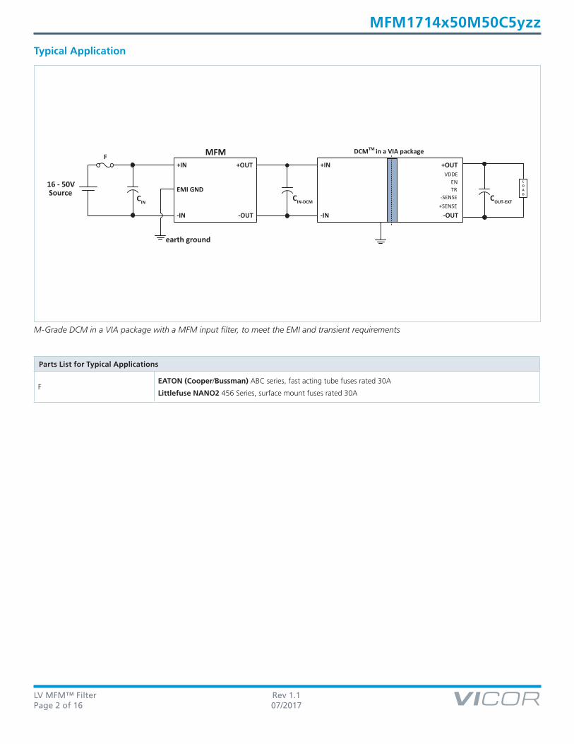
EMI/EMC
Standard Test Procedure Notes
MIL-STD-461E/F
Conducted EmmisionsCE101 Figure CE101-4, Navy ASW & Army Aircraft, Curve #2 (28VDC or below)
CE102 Figure CE102-1, Basic curve for all applications
Conducted Susceptibility CS101 Figure CS101, Curve #2, for all applications (28VDC or below)
MIL-STD-1275
Transient Immunity [4] MIL-STD-1275A/B/D/E100VDC for 50ms duration
250VDC for 70µs
MIL-STD-704
Transient Immunity [4]
MIL-STD-704A (MIL-HDBK-704-8) Normal Voltage Transients
From table LDC 105-II (A-J) overvoltage 70VDC for 20ms duration; within the MIL-STD-1275 (100V for 50ms) transient condition
MIL-STD-704B/C/D/E/F (MIL-HDBK-704-8) Normal Voltage Transients
From table LDC 105-III (AA-RR) overvoltage 50VDC for 12.5ms duration, undervoltage 18VDC for 15ms duration; within the normal operating input voltage range
MIL-STD-704A (MIL-HDBK-704-8) Abnormal Voltage Transients
From table LDC 302-II (A-J) overvoltage 80VDC for 50ms duration; within the MIL-STD-1275 (100V for 50ms) transient condition
MIL-STD-704E/F (MIL-HDBK-704-8) Abnormal Voltage Transients
From Table LDC 302-IV (AAA-FFF), overvoltage test conditions; within the normal operating input voltage range
DO-160E
Transient Immunity [4] DO-160E sec. 16, cat. z 80VDC for 100ms
[4] Transient immunity specifications are met only when LV MFM is used with M-grade 16-50VIN DCM in a VIA package.
LV MFM™ Filter Rev 1.1Page 6 of 16 07/2017
MFM1714x50M50C5yzz
Typical Characteristics
Frequency (Hz)Common Mode
-60
-70
-80
-901k100 10k 100k 1M 10M
-50
-40
-30
-20
-10
0
Differential Mode
Atte
nuat
ion
(dB
)
F/Hz CM-Mode DF-ModeCursor 1 100k -33.201dB -38.75dBCursor 2 1M -68.687dB -61.283dB
100 1k 10k 100k 1M 10M
-40
-20
20
0
40
0
50
100
150
200
250
300
350
400
Out
put I
mpe
danc
e M
angi
tude
Z (d
BΩ
):
Out
put I
mpe
danc
e M
angi
tude
Z (Ω
)
Frequency (Hz)Output Impedance Z (dBΩ) Output Impedance Z (Ω)
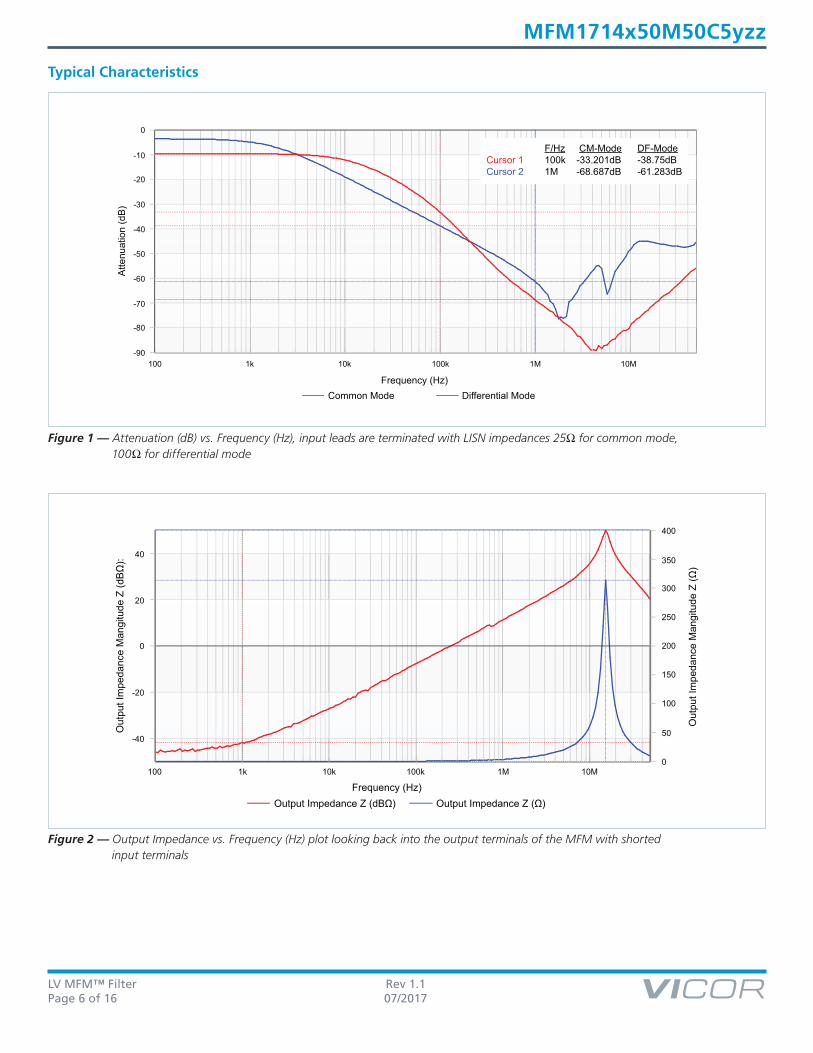
Figure 1 — Attenuation (dB) vs. Frequency (Hz), input leads are terminated with LISN impedances 25Ω for common mode, 100Ω for differential mode
Figure 2 — Output Impedance vs. Frequency (Hz) plot looking back into the output terminals of the MFM with shorted input terminals

LV MFM™ Filter Rev 1.1Page 7 of 16 07/2017
MFM1714x50M50C5yzz
Typical Conducted Emissions
CE101 peak scans with MFM1714V50M50C5M00 and DCM3414V50M31C2T01, –OUT connected to GND, –OUT floating.
30 Hz 10 kHz
SGL
1MA
Unit dB A
Trd CE101
23.Nov 2016 14:25
ResBW 100 Hz
Meas T 20 ms
Det MA
Att 10 dB
INPUT 2
100 Hz 1 kHz 10 kHz
10
20
30
40
50
60
70
80
90
100
110
120
130
0
140
CE101-42
Date: 23.NOV.2016 14:25:39
30 Hz 10 kHz
SGL
1MA
Unit dB A
Trd CE101
ResBW 100 Hz
Meas T 20 ms
Det MA
Att 10 dB
INPUT 2
23.Nov 2016 14:06
100 Hz 1 kHz 10 kHz
10
20
30
40
50
60
70
80
90
100
110
120
130
0
140
1
Marker 1 [T1]
86.36 dB A
318.00000000 Hz
1 [T1] 86.36 dB A
318.00000000 Hz
CE101-42
Date: 23.NOV.2016 14:06:27
30 Hz 10 kHz
SGL
1MA
Unit dB A
Trd CE101
23.Nov 2016 14:40
Det MA
ResBW 10 Hz
Meas T 20 ms
Att 10 dB
INPUT 2
100 Hz 1 kHz 10 kHz
10
20
30
40
50
60
70
80
90
100
110
120
130
0
140
1
Marker 1 [T1]
84.68 dB A
338.00000000 Hz
1 [T1] 84.68 dB A
338.00000000 Hz
CE101-42
Date: 23.NOV.2016 14:40:36
Figure 4 — Peak scan for the RED lead with CIN = 2200µF, COUT-EXT = 1000µF, 0% load
Figure 7 — Peak scan for the BLACK lead with CIN = 2200µF, COUT-EXT = 1000µF, 100% load
Figure 5 — Peak scan for the RED lead with CIN = 2200µF, COUT-EXT = 1000µF, 100% load
30 Hz 10 kHz
SGL
1MA
Unit dB A
Trd CE101
ResBW 100 Hz
Meas T 20 ms
Det MA
Att 10 dB
INPUT 2
23.Nov 2016 14:21
100 Hz 1 kHz 10 kHz
10
20
30
40
50
60
70
80
90
100
110
120
130
0
140
CE101-42
Date: 23.NOV.2016 14:21:38
Figure 6 — Peak scan for the BLACK lead with CIN = 2200µF, COUT-EXT = 1000µF, 0% load
DC Power Supply
ScreenRoom/Filters
LISN
LISN
LV MFM
+IN
-IN
+OUT
-OUT
+IN
-IN
+OUT
-OUT
Load
50Ω Termination onSignal Output Port(One for Each LISN)
EMIReceiver
Current Probe
EMI GND
+
-
CIN COUT
DCMTM in a VIA Package
Figure 3 — A typical test setup for conducted emissions CE101 is shown above. A current probe is used to measure and plot the variations in the current through the RED and BLACK leads at various load conditions.
LV MFM™ Filter Rev 1.1Page 8 of 16 07/2017
MFM1714x50M50C5yzz
Typical Conducted Emissions (Cont.)
CE102 peak scans with MFM1714V50M50C5M00 and DCM3414V50M31C2T01, –OUT connected to GND, –OUT floating.
SGL
1MA
10 kHz 10 MHz
Unit dB V
Trd CE102RED
30.Nov 2016 15:24
ResBW 10 kHz
Meas T 20 ms
Det MA
Att 10 dB
INPUT 2
100 kHz 1 MHz 10 MHz
20
30
40
50
60
70
80
90
100
10
110
1
Marker 1 [T1]
67.96 dB V
40.40000000 kHz
1 [T1] 67.96 dB V
40.40000000 kHz
CE10228
Date: 30.NOV.2016 15:24:45
SGL
1MA
10 kHz 10 MHz
Unit dB V
Trd CE102BLK
30.Nov 2016 15:32
ResBW 10 kHz
Meas T 20 ms
Det MA
Att 10 dB
INPUT 2
100 kHz 1 MHz 10 MHz
20
30
40
50
60
70
80
90
100
10
110
1
Marker 1 [T1]
72.98 dB V
40.40000000 kHz
1 [T1] 72.98 dB V
40.40000000 kHz
CE10228
Date: 30.NOV.2016 15:32:50
SGL
1MA
10 kHz 10 MHz
Unit dB V
Trd CE102RED
ResBW 10 kHz
Meas T 20 ms
Det MA
Att 10 dB
INPUT 2
30.Nov 2016 15:19
100 kHz 1 MHz 10 MHz
20
30
40
50
60
70
80
90
100
10
110
1
Marker 1 [T1]
73.00 dB V
40.40000000 kHz
1 [T1] 73.00 dB V
40.40000000 kHz
CE10228
Date: 30.NOV.2016 15:19:13
Figure 9— Peak scan for the RED lead with CIN = 2200µF, CIN-DCM = 1000µF, COUT-EXT = 1000µF, 0% load
Figure 12 — Peak scan for the BLACK lead with CIN = 2200µF, CIN-DCM = 1000µF, COUT-EXT = 1000µF, 100% load
Figure 10 — Peak scan for the RED lead with CIN = 2200µF, CIN-DCM = 1000µF, COUT-EXT = 1000µF, 100% load
SGL
1MA
10 kHz 10 MHz
Unit dB V
Trd CE102BLK
30.Nov 2016 15:26
ResBW 10 kHz
Meas T 20 ms
Det MA
Att 10 dB
INPUT 2
100 kHz 1 MHz 10 MHz
20
30
40
50
60
70
80
90
100
10
110
1
Marker 1 [T1]
68.19 dB V
40.40000000 kHz
1 [T1] 68.19 dB V
40.40000000 kHz
CE10228
Date: 30.NOV.2016 15:26:59
Figure 11 — Peak scan for the BLACK lead with CIN = 2200µF, CIN-DCM = 1000µF, COUT-EXT = 1000µF, 0% load
DC Power Supply
ScreenRoom/Filters
LISN
LISN
50Ω Termination
+
-
EMI Reciever
20dB Attenuator
LV MFM-IN
+IN +OUT
-OUT
Load
EMI GND
DCM™ in a VIA Package
CIN-DCMCIN COUT
-IN
+IN +OUT
-OUT
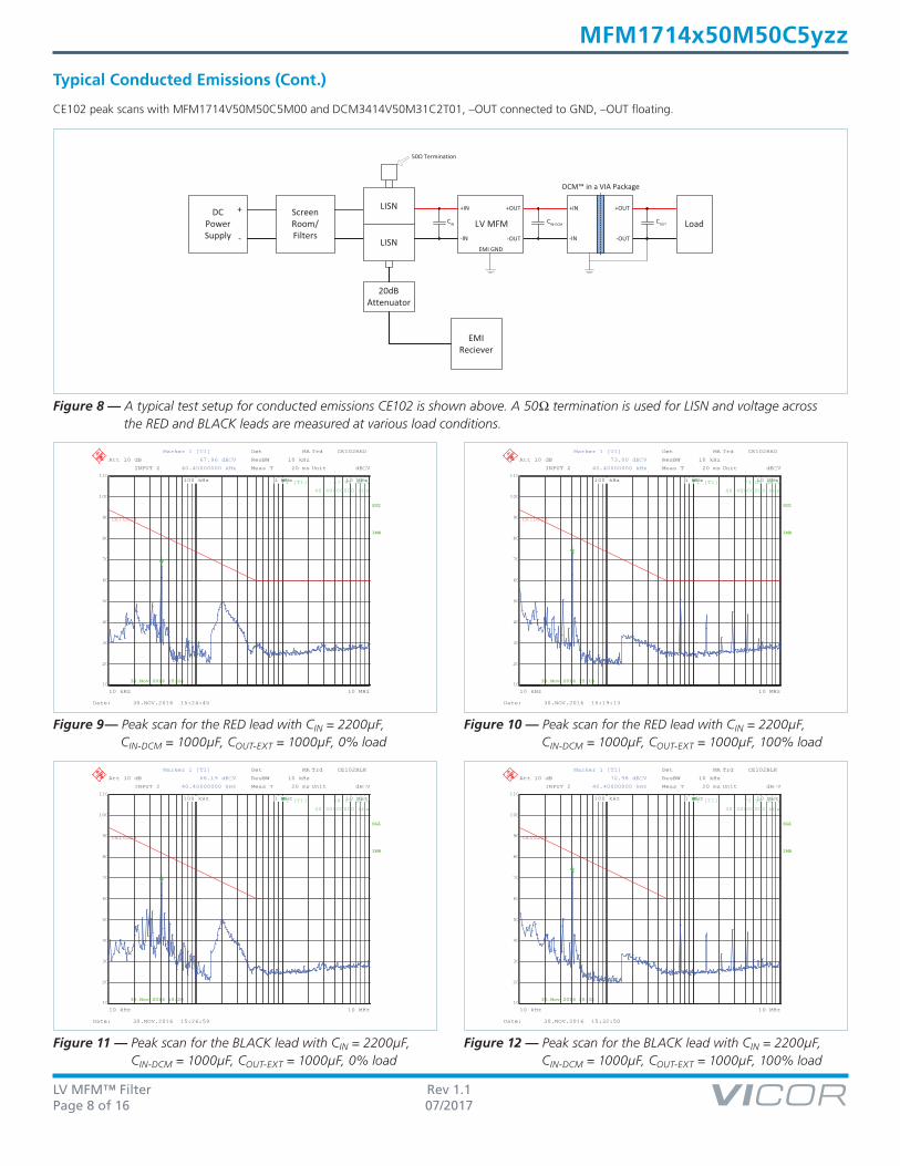
Figure 8 — A typical test setup for conducted emissions CE102 is shown above. A 50Ω termination is used for LISN and voltage across the RED and BLACK leads are measured at various load conditions.

LV MFM™ Filter Rev 1.1Page 9 of 16 07/2017
MFM1714x50M50C5yzz
Electrical Power Characteristics
Transient immunity with MFM1714V50M50C5M00 and DCM3414V50M13C2M01 per MIL-STD-1275D/E.
Figure 13 — Transient immunity; LV MFM and DCM 3414 VIA output response to an 100V, 50ms input transient
LV MFM™ Filter Rev 1.1Page 10 of 16 07/2017
MFM1714x50M50C5yzz
General Characteristics
Specifications apply over all line and load conditions, TJ = 25°C, unless otherwise noted; boldface specifications apply over the temperature range of the specified product grade.
Attribute Symbol Conditions / Notes Min Typ Max Unit
Mechanical
Length L 44.6 / [1.76] mm / [in]
Width W 35.5 / [1.39] mm / [in]
Height H 9.22 / [0.36] mm / [in]
Volume Vol Without heatsink 14.5 / [0.88] cm3/ [in3]
Mass (Weight) M 30 / [1.06] g / [oz]
Pin Material C145 copper, 1/2 hard
Underplate Low stress ductile Nickel 50 100 µin
Pin FinishPalladium 0.8 6
µinSoft Gold 0.12 2
Flatness <0.25 / [0.010] mm / [in]
Thermal
Internal Operating Temperature M-Grade -55 125°C
Case Temperature M-Grade -55 100
Thermal Resistance, Junction to Case Bottom
θINT_BOT 14.29 °C/W
Thermal Resistance, Junction to Output Terminals
θINT_OUT_
TERMINALS4.68 °C/W
Soldering
TemperatureSee: AN:401 PCB Mount VIA Soldering Guidelines
Reliability
MTBF MIL-HDBK-217FN2 Parts Count - 25°C Ground Benign, Stationary, Indoors / Computer
6.6 MHrs
Safety
Dielectric Withstand Input / Output to EMI GND/Case 1500 VDC
Agency Approvals / Standards
CE marked to the Low Voltage Directive (LVD) 2014/35/EU

LV MFM™ Filter Rev 1.1Page 11 of 16 07/2017
MFM1714x50M50C5yzz
Environmental Qualification
Testing Activity Reference Standard Test Details
HTOB-HTOL High Temperature Operating Bias/Life
JESD22-A110-BDuration of 1000 hrs, High Line, full load, max operating temperature, Power cycled per IPC9592
TC (Temperature Cycling) JESD22-A104D 1000 cycles -55°C to 125°C
HALT (Highly Accelerated Life Test) DP-0266Low Temp, High Temp, Rapid Thermal Cycling, Random Vibration Test, Combined Stress Test
THB (Temperature Humidity Bias) JEDSD22-A101C Duration of 1000hrs, Biased, 85°C, 85%RH.
HTS (High Temperature Storage) JESD 22-A103-DDuration 1000hrs, No Bias. Maximum storage temperature (125°C)
LTS (Low Temperature Storage) JESD22–A119Duration 1000hrs, No Bias. Minimum storage temperature (-65°C)
Random Vibration MIL-STD-810G Method 514.6, Procedure I, Category 24, Mounted on QA
Mechanical Shock MIL-STD-810GMethod 516.5, Procedure I, Environment: Functional shock 40G, Mounted on QA
Electro Static Discharge Human Body Model JEDEC JS-001-2012 Table 2B, Class 2, ±2000V minimum
Electro Static Discharge Device Charge Model
JESD22-C101-E Class III ±500V minimum
Free Fall IPC9592B IEC 60068-2-32, Freefall procedure 1
Term Strength MIL-STD-202GMethod 211A,Test Condition A, Environment: Ambient Temperature & %Rh.
Through Hole Solderability IPC-9592B IPC/ECA J-STD-002 Test A (dip and look)
Salt Fog MIL-STD-810G Method 509.5
Fungus MIL-STD-810G Method 508.6
Resistance to solvents MIL-STD-202G Method 215K
Acceleration MIL-STD-810G Method 513.6 Procedure II
Altitude MIL-STD-810G Method 500.5 Procedure I & II
Explosive Atmosphere MIL-STD-810G Method 511.5 Procedure I, operational
LV MFM™ Filter Rev 1.1Page 12 of 16 07/2017
MFM1714x50M50C5yzz
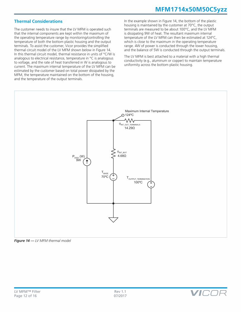
Maximum Internal Temperature124ºC
PDISS (W)9W
θINT_OUT_TERMINALS
14.29Ω
θINT_BOT
4.68Ω
TBASE
70ºC TOUTPUT_TERMINATION
100ºC
Thermal Considerations
The customer needs to insure that the LV MFM is operated such that the internal components are kept within the maximum of the operating temperature range by monitoring/controlling the temperature of both the bottom plastic housing and the output terminals. To assist the customer, Vicor provides the simplified thermal circuit model of the LV MFM shown below in Figure 14. In this thermal circuit model, thermal resistance in units of °C/W is analogous to electrical resistance, temperature in °C is analogous to voltage, and the rate of heat transferred in W is analogous to current. The maximum internal temperature of the LV MFM can be estimated by the customer based on total power dissipated by the MFM, the temperature maintained on the bottom of the housing, and the temperature of the output terminals.
In the example shown in Figure 14, the bottom of the plastic housing is maintained by the customer at 70°C, the output terminals are measured to be about 100°C, and the LV MFM is dissipating 9W of heat. The resultant maximum internal temperature of the LV MFM can then be estimated at 124°C, which is close to the maximum in the operating temperature range. 4W of power is conducted through the lower housing, and the balance of 5W is conducted through the output terminals.
The LV MFM is best attached to a material with a high thermal conductivity (e.g., aluminum or copper) to maintain temperature uniformity across the bottom plastic housing.
Figure 14 — LV MFM thermal model

LV MFM™ Filter Rev 1.1Page 13 of 16 07/2017
MFM1714x50M50C5yzz
1.17029.720
.112.82
.8822.28
.15
3.86(2) PL.
PIN 1 DESIGNATOR
EMIGND
-IN -OUT
+OUT+IN
.37±.0159.30±.381
1.7644.60
1.4035.50
Chassis Mount Outline Drawing

LV MFM™ Filter Rev 1.1Page 14 of 16 07/2017
MFM1714x50M50C5yzz
.37±.0159.30±.381
.0802.032(5) PL.
DIM 'L'±.015(5) PL.
SEATING PLANE
1.7644.60
.112.89
.8822.30
1.17029.718
TOP VIEW(COMPONENT SIDE)
.153.86
(2) PL.
1.396±.01035.458±.254
.698±.01017.729±.254
.474±.01012.029±.254
(2) PL.
.947±.01024.058±.254
.111±.0102.825±.254
BOTTOM VIEW
+IN
EMIGND
-IN -OUT
+OUT
1.4035.50
DIM 'L'SHORT .120 [3.026]LONG .199 [5.042]
1.396±.00335.452±.076
.698±.00317.726±.076
.474±.00312.029±.076
(2) PL.
.947±.00324.058±.076
1.170±.00329.720±.076
.111±.0032.831±.076
.120±.003
3.048±.076PLATED THRU
.030 [.762]ANNULAR RING
(5) PL.
.172±.0034.369±.076
PLATED THRU.064 [1.626]
ANNULAR RING(2) PL.
RECOMMENDED HOLE PATTERN(COMPONENT SIDE)
-OUT
+OUT+IN
EMIGND
-IN
Board Mount Outline Drawing
LV MFM™ Filter Rev 1.1Page 15 of 16 07/2017
MFM1714x50M50C5yzz
Revision History
Revision Date Description Page Number(s)
1.0 06/07/17 Initial Release n/a
1.1 07/26/17
Added fuse recommendation for typical application & remvoed MOVUpdated internal operting temperatureUpdated note on CE scans for –OUT floatingUpdated MTBF rating
24
7, 810

LV MFM™ Filter Rev 1.1Page 16 of 16 07/2017
MFM1714x50M50C5yzz
Vicor’s comprehensive line of power solutions includes high density AC-DC and DC-DC modules and accessory components, fully configurable AC-DC and DC-DC power supplies, and complete custom power systems.
Information furnished by Vicor is believed to be accurate and reliable. However, no responsibility is assumed by Vicor for its use. Vicor makes no representations or warranties with respect to the accuracy or completeness of the contents of this publication. Vicor reserves the right to make changes to any products, specifications, and product descriptions at any time without notice. Information published by Vicor has been checked and is believed to be accurate at the time it was printed; however, Vicor assumes no responsibility for inaccuracies. Testing and other quality controls are used to the extent Vicor deems necessary to support Vicor’s product warranty. Except where mandated by government requirements, testing of all parameters of each product is not necessarily performed.
Specifications are subject to change without notice.
Visit http://www.vicorpower.com/mil-cots-dc-dc/mfm-filter-module for the latest product information.
Vicor’s Standard Terms and Conditions and Product WarrantyAll sales are subject to Vicor’s Standard Terms and Conditions of Sale, and Product Warranty which are available on Vicor’s webpage (http://www.vicorpower.com/termsconditionswarranty) or upon request.
Life Support Policy
VICOR’S PRODUCTS ARE NOT AUTHORIZED FOR USE AS CRITICAL COMPONENTS IN LIFE SUPPORT DEVICES OR SYSTEMS WITHOUT THE EXPRESS PRIOR WRITTEN APPROVAL OF THE CHIEF EXECUTIVE OFFICER AND GENERAL COUNSEL OF VICOR CORPORATION. As used herein, life support devices or systems are devices which (a) are intended for surgical implant into the body, or (b) support or sustain life and whose failure to perform when properly used in accordance with instructions for use provided in the labeling can be reasonably expected to result in a significant injury to the user. A critical component is any component in a life support device or system whose failure to perform can be reasonably expected to cause the failure of the life support device or system or to affect its safety or effectiveness. Per Vicor Terms and Conditions of Sale, the user of Vicor products and components in life support applications assumes all risks of such use and indemnifies Vicor against all liability and damages.
Intellectual Property Notice
Vicor and its subsidiaries own Intellectual Property (including issued U.S. and Foreign Patents and pending patent applications) relating to the products described in this data sheet. No license, whether express, implied, or arising by estoppel or otherwise, to any intellectual property rights is granted by this document. Interested parties should contact Vicor’s Intellectual Property Department.
The products described on this data sheet are protected by the following U.S. Patents Numbers:Patents Pending.
Contact Us: http://www.vicorpower.com/contact-us
Vicor Corporation25 Frontage Road
Andover, MA, USA 01810Tel: 800-735-6200Fax: 978-475-6715
www.vicorpower.com
emailCustomer Service: [email protected]
Technical Support: [email protected]
©2017 Vicor Corporation. All rights reserved. The Vicor name is a registered trademark of Vicor Corporation.All other trademarks, product names, logos and brands are property of their respective owners.