Embed Size (px)
Citation preview
Operational Amplifier
XMUT303 Analogue Electronics

Topics
• Basic characteristics and properties.
• Device imperfections.
• Circuit limitations.
• Design problems and solutions.
OperationalAmplifiers
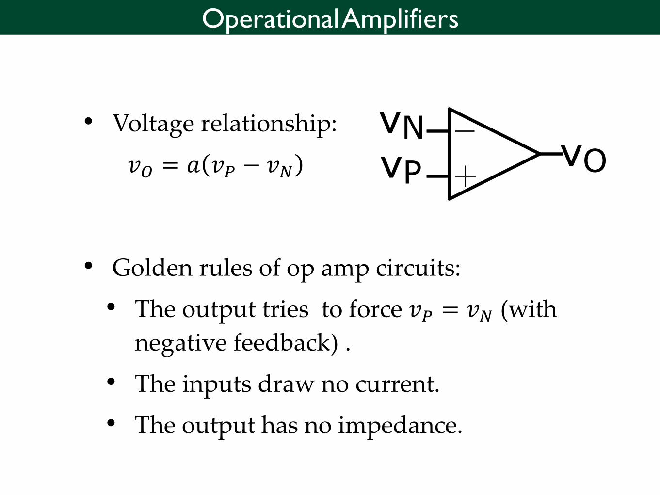
• Voltage relationship:
𝑣𝑂 = 𝑎 𝑣𝑃 − 𝑣𝑁
• Golden rules of op amp circuits:
• The output tries to force 𝑣𝑃 = 𝑣𝑁 (with
negative feedback) .
• The inputs draw no current.
• The output has no impedance.
vNvP vO
Impedance
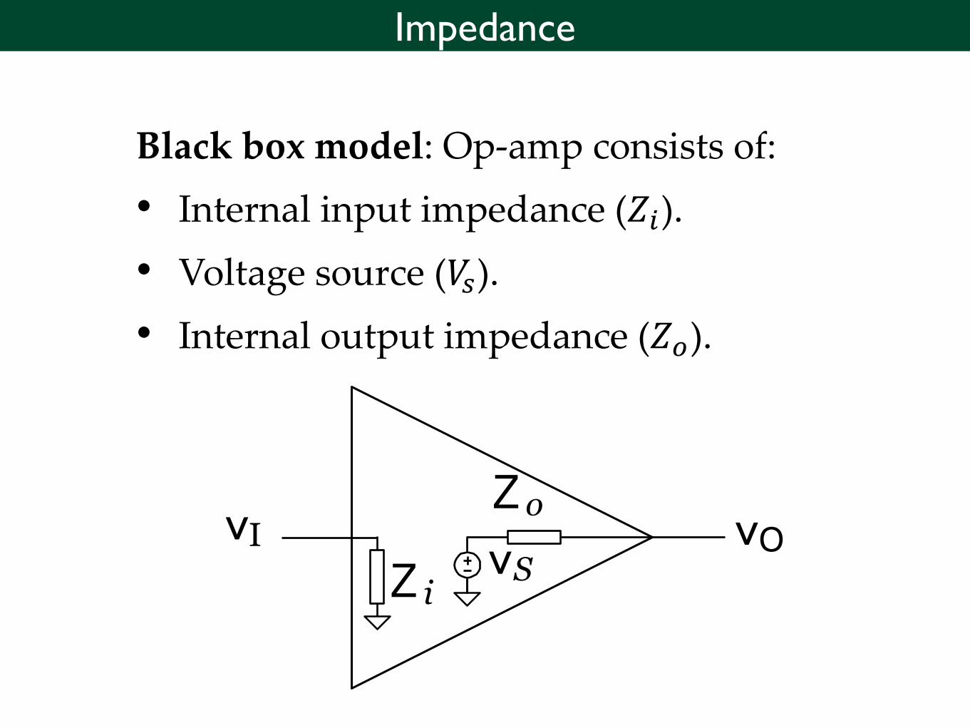
Black box model: Op-amp consists of:
• Internal input impedance (𝑍𝑖).
• Voltage source (𝑉𝑠).
• Internal output impedance (𝑍𝑜).
vIZ i
vOZovS
Impedance (Input Side)
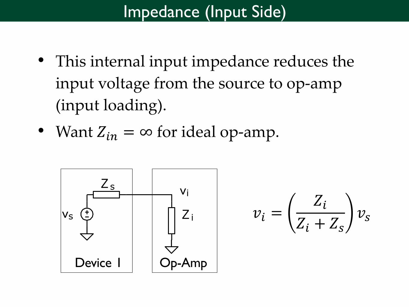
• This internal input impedance reduces the
input voltage from the source to op-amp
(input loading).
• Want 𝑍𝑖𝑛 = ∞ for ideal op-amp.
Z s
vs
Device 1 Op-Amp
vi
Z i 𝑣𝑖 =𝑍𝑖
𝑍𝑖 + 𝑍𝑠𝑣𝑠
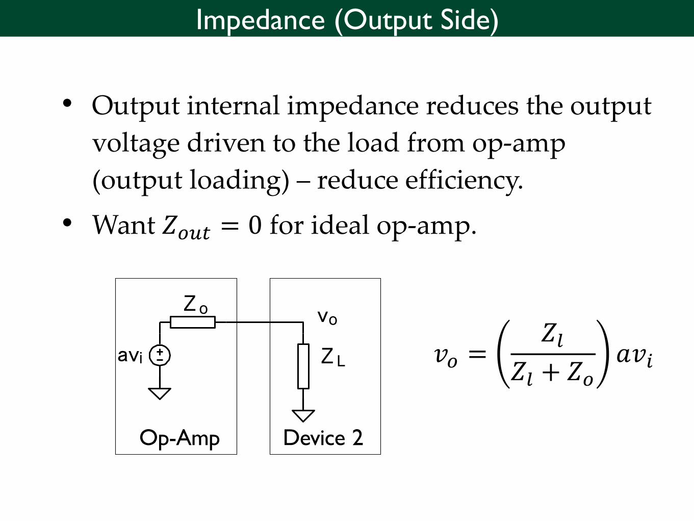
Impedance (Output Side)
• Output internal impedance reduces the output
voltage driven to the load from op-amp
(output loading) – reduce efficiency.
• Want 𝑍𝑜𝑢𝑡 = 0 for ideal op-amp.
Zo
avi
Op-Amp Device 2
vo
Z L 𝑣𝑜 =𝑍𝑙
𝑍𝑙 + 𝑍𝑜𝑎𝑣𝑖
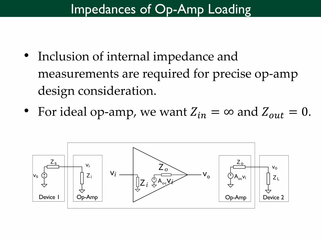
Impedances of Op-Amp Loading
• Inclusion of internal impedance and
measurements are required for precise op-amp
design consideration.
• For ideal op-amp, we want 𝑍𝑖𝑛 = ∞ and 𝑍𝑜𝑢𝑡 = 0.
viZ i
voZ o
Aocvi
Zs
vs
Device 1 Op-Amp
vi
Z i
Zo
ZLAocvi
Op-Amp Device 2
vo
Impedances of Op-Amp Loading
viZ i
vo
Z o
Aocvi
Zs
vs
Input
Source Op-Amp
vi
Z i
Zo
ZLAocvi
Op-Amp Load
vo
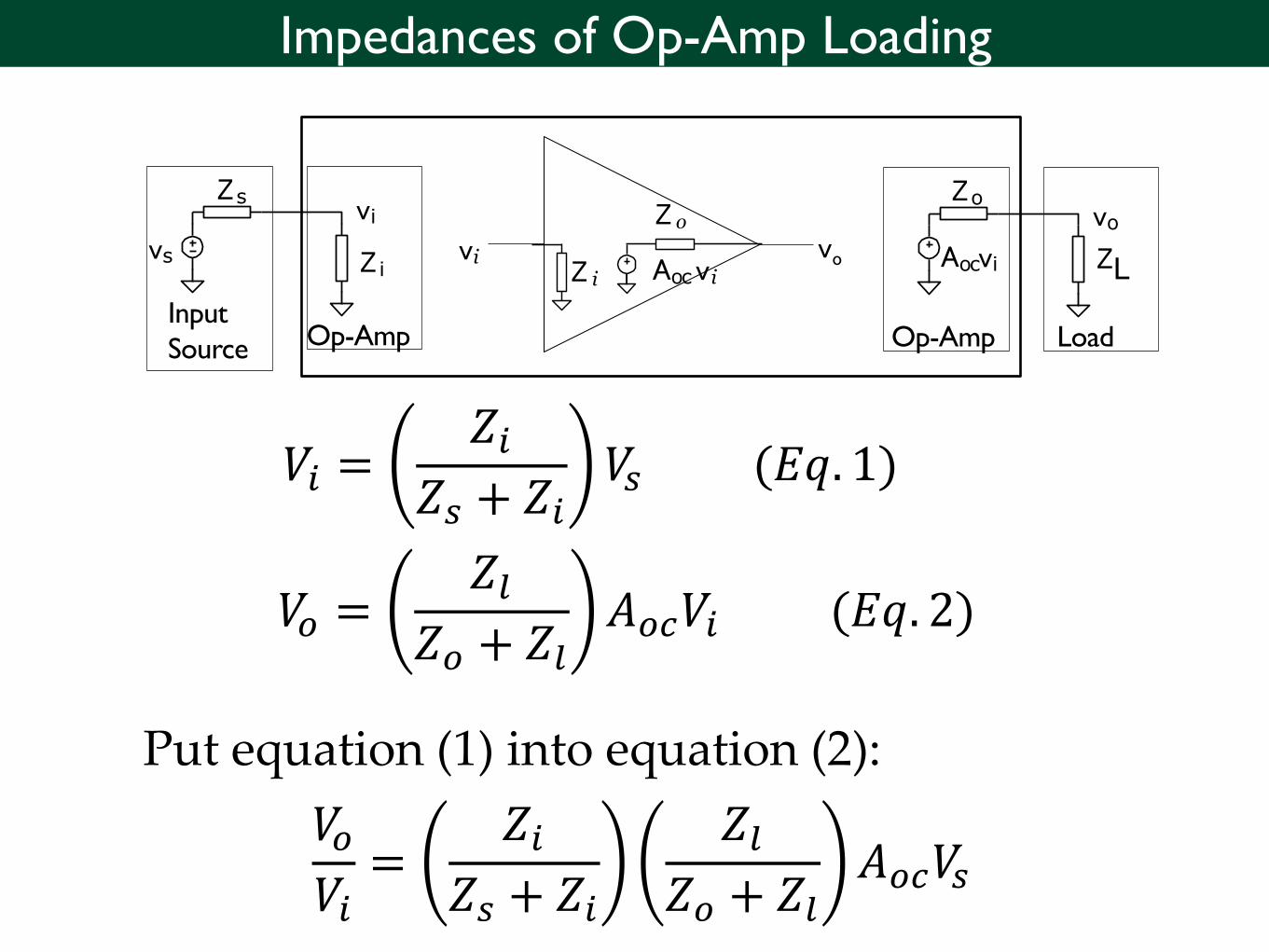
Put equation (1) into equation (2):
𝑉𝑜𝑉𝑖
=𝑍𝑖
𝑍𝑠 + 𝑍𝑖
𝑍𝑙𝑍𝑜 + 𝑍𝑙
𝐴𝑜𝑐𝑉𝑠
𝑉𝑖 =𝑍𝑖
𝑍𝑠 + 𝑍𝑖𝑉𝑠 (𝐸𝑞. 1)
𝑉𝑜 =𝑍𝑙
𝑍𝑜 + 𝑍𝑙𝐴𝑜𝑐𝑉𝑖 (𝐸𝑞. 2)
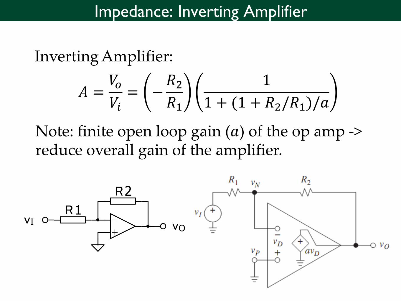
Impedance: Inverting Amplifier
R1
R2
vOvI
Inverting Amplifier:
𝐴 =𝑉𝑜𝑉𝑖
= −𝑅2𝑅1
1
1 + (1 + 𝑅2/𝑅1)/𝑎
Note: finite open loop gain (𝑎) of the op amp -> reduce overall gain of the amplifier.
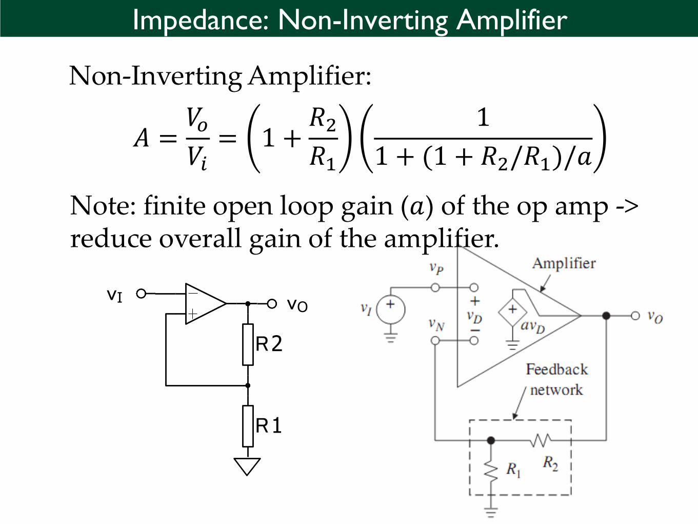
Impedance: Non-Inverting Amplifier
Non-Inverting Amplifier:
𝐴 =𝑉𝑜𝑉𝑖
= 1 +𝑅2𝑅1
1
1 + (1 + 𝑅2/𝑅1)/𝑎
R1
R2
vOvI
Note: finite open loop gain (𝑎) of the op amp -> reduce overall gain of the amplifier.
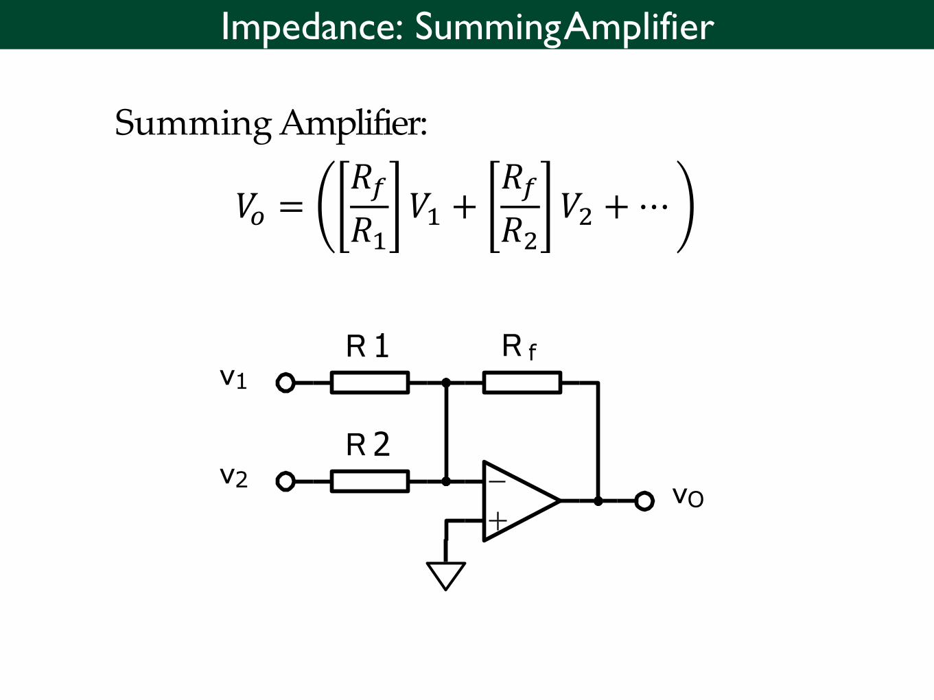
Impedance: SummingAmplifier
Summing Amplifier:
𝑉𝑜 =𝑅𝑓
𝑅1𝑉1 +
𝑅𝑓
𝑅2𝑉2 +⋯
v2 vO
R 2
R fR 1v1
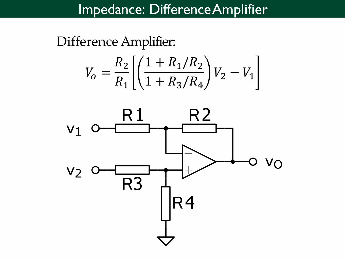
Impedance: DifferenceAmplifier
R1 R2
vO
v1
R3R4
v2
Difference Amplifier:
𝑉𝑜 =𝑅2𝑅1
1 + 𝑅1/𝑅21 + 𝑅3/𝑅4
𝑉2 − 𝑉1
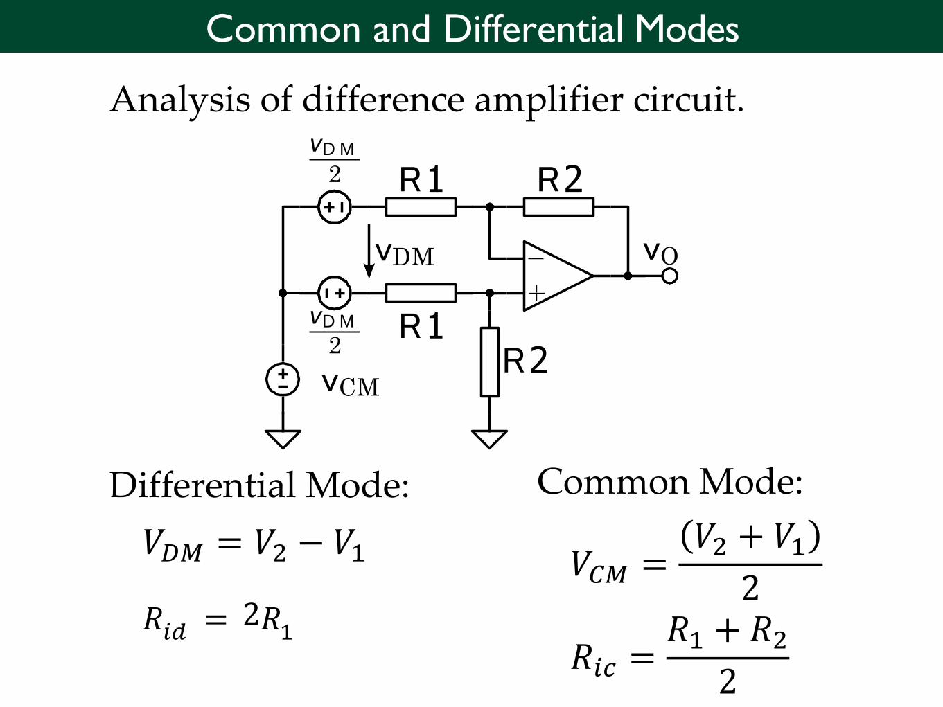
Common and Differential Modes
Differential Mode:
𝑉𝐷𝑀 = 𝑉2 − 𝑉1
𝑅𝑖𝑑 = 2𝑅1
Common Mode:
𝑉𝐶𝑀 =𝑉2 + 𝑉1
2
𝑅𝑖𝑐 =𝑅1 + 𝑅2
2
R1 R2
vO
R2R1
vD M
2
vD M
2
vCM
vDM
Analysis of difference amplifier circuit.
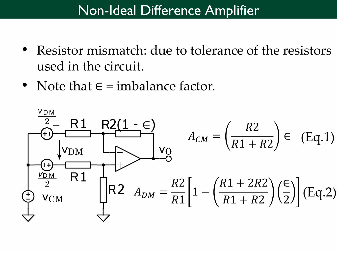
Non-Ideal Difference Amplifier
• Resistor mismatch: due to tolerance of the resistors used in the circuit.
• Note that ∈ = imbalance factor.
R1 R2(1 - ∈)
vO
R2R1
vD M
2
vD M
2
vCM
vDM𝐴𝐶𝑀 =
𝑅2
𝑅1 + 𝑅2∈
𝐴𝐷𝑀 =𝑅2
𝑅11 −
𝑅1 + 2𝑅2
𝑅1 + 𝑅2
∈
2
(Eq.1)
(Eq.2)

Difference Amplifier Calibration
R1 R2
vO
R3R4
—vcalib
R calib
+vcalib
Circuit calibration:
• Trimming using Howland circuit.
• Downside: increase cost of production.
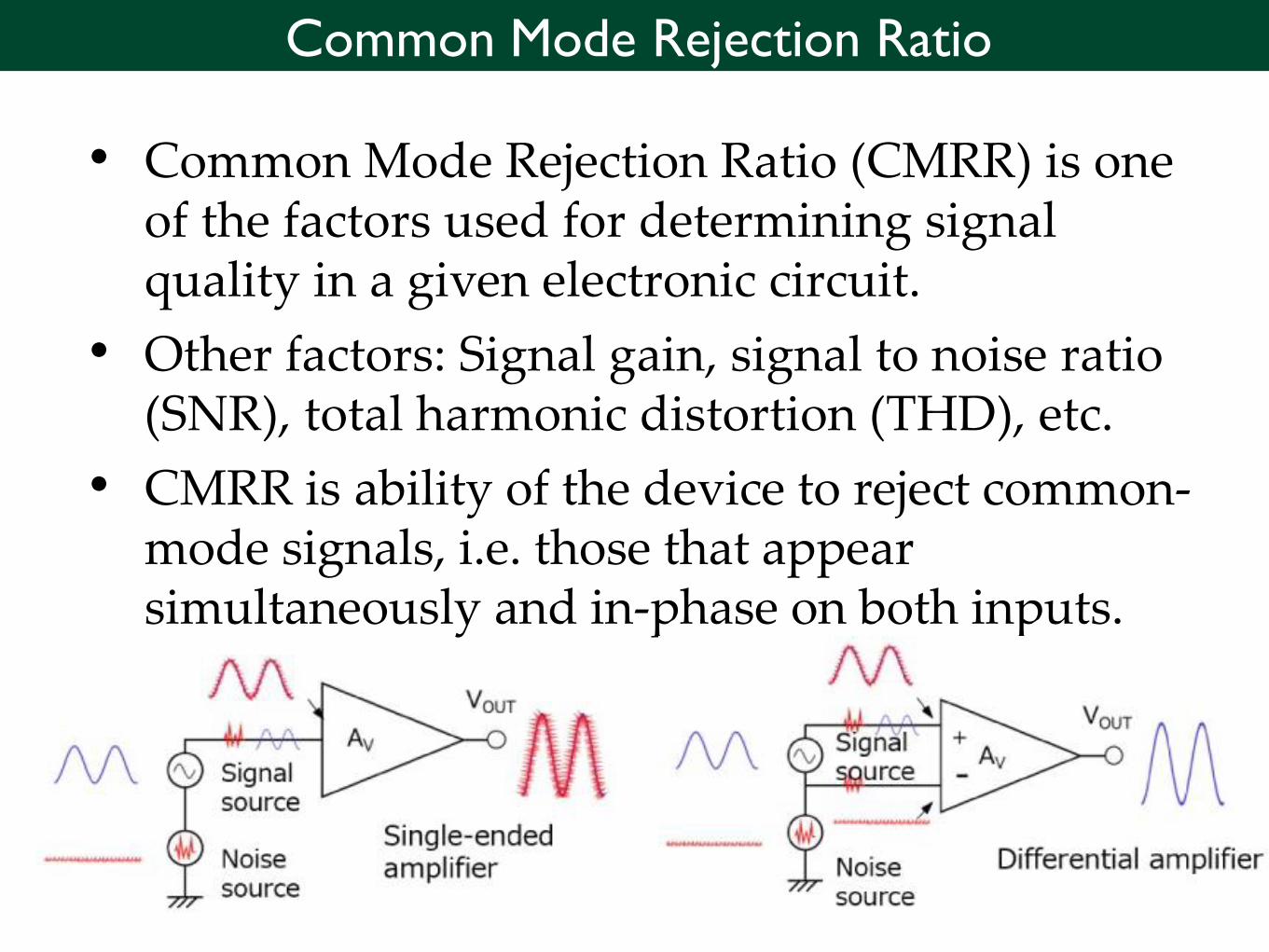
Common Mode Rejection Ratio
• Common Mode Rejection Ratio (CMRR) is one of the factors used for determining signal quality in a given electronic circuit.
• Other factors: Signal gain, signal to noise ratio (SNR), total harmonic distortion (THD), etc.
• CMRR is ability of the device to reject common-mode signals, i.e. those that appear simultaneously and in-phase on both inputs.
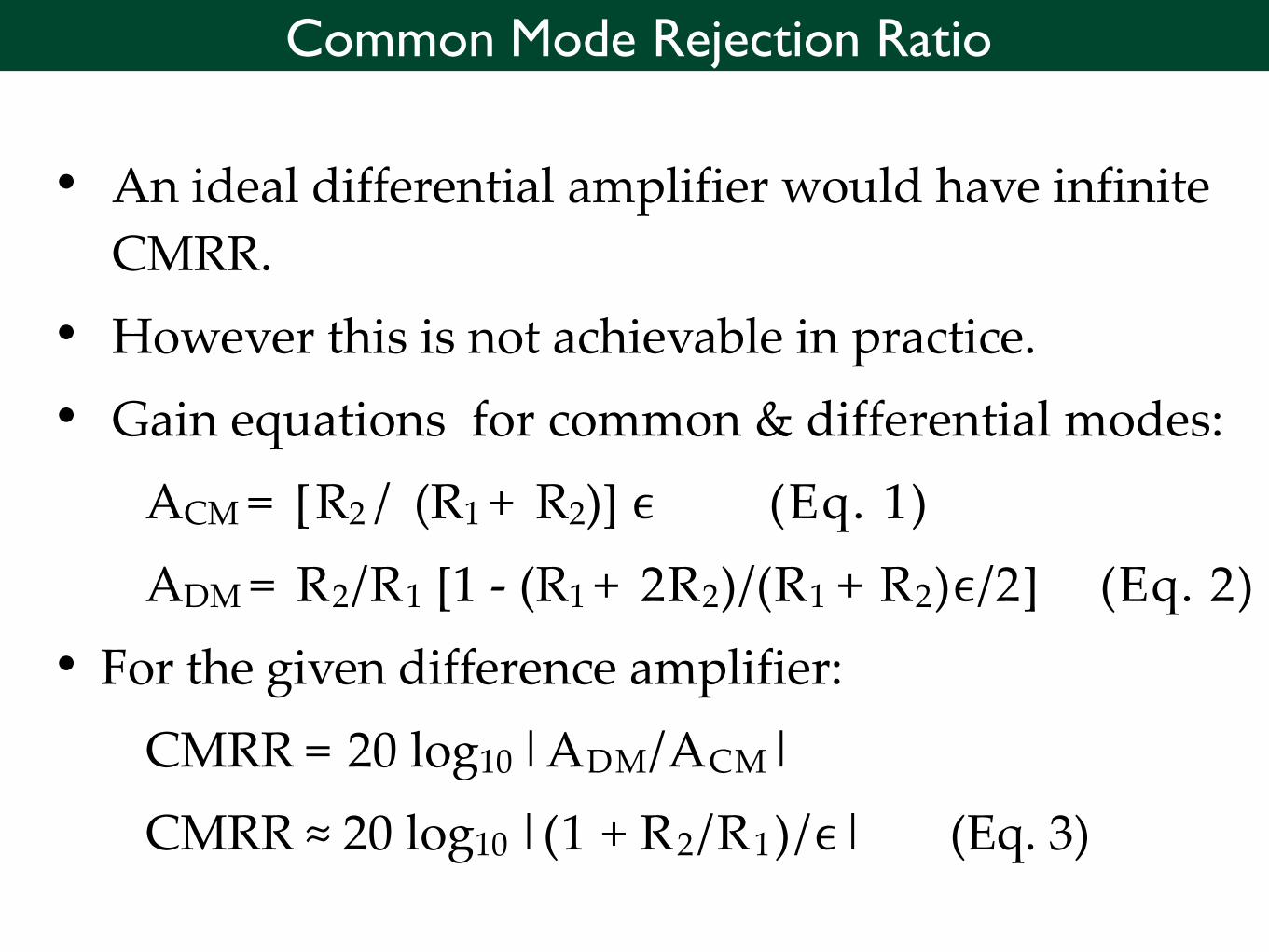
Common Mode Rejection Ratio
• An ideal differential amplifier would have infinite
CMRR.
• However this is not achievable in practice.
• Gain equations for common & differential modes:
ACM = [R2 / (R1 + R2)] ϵ (Eq. 1)
ADM = R2/R1 [1 - (R1 + 2R2)/(R1 + R2)ϵ/2] (Eq. 2)
• For the given difference amplifier:
CMRR = 20 log10 |ADM/ACM|
CMRR ≈ 20 log10 |(1 + R2/R1)/ϵ| (Eq. 3)
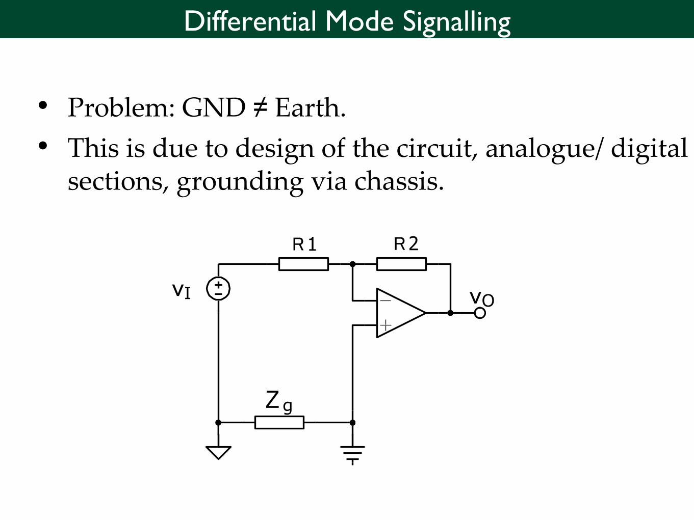
Differential Mode Signalling
• Problem: GND ≠ Earth.
• This is due to design of the circuit, analogue/ digital sections, grounding via chassis.
vO
Zg
vI
R 1 R 2
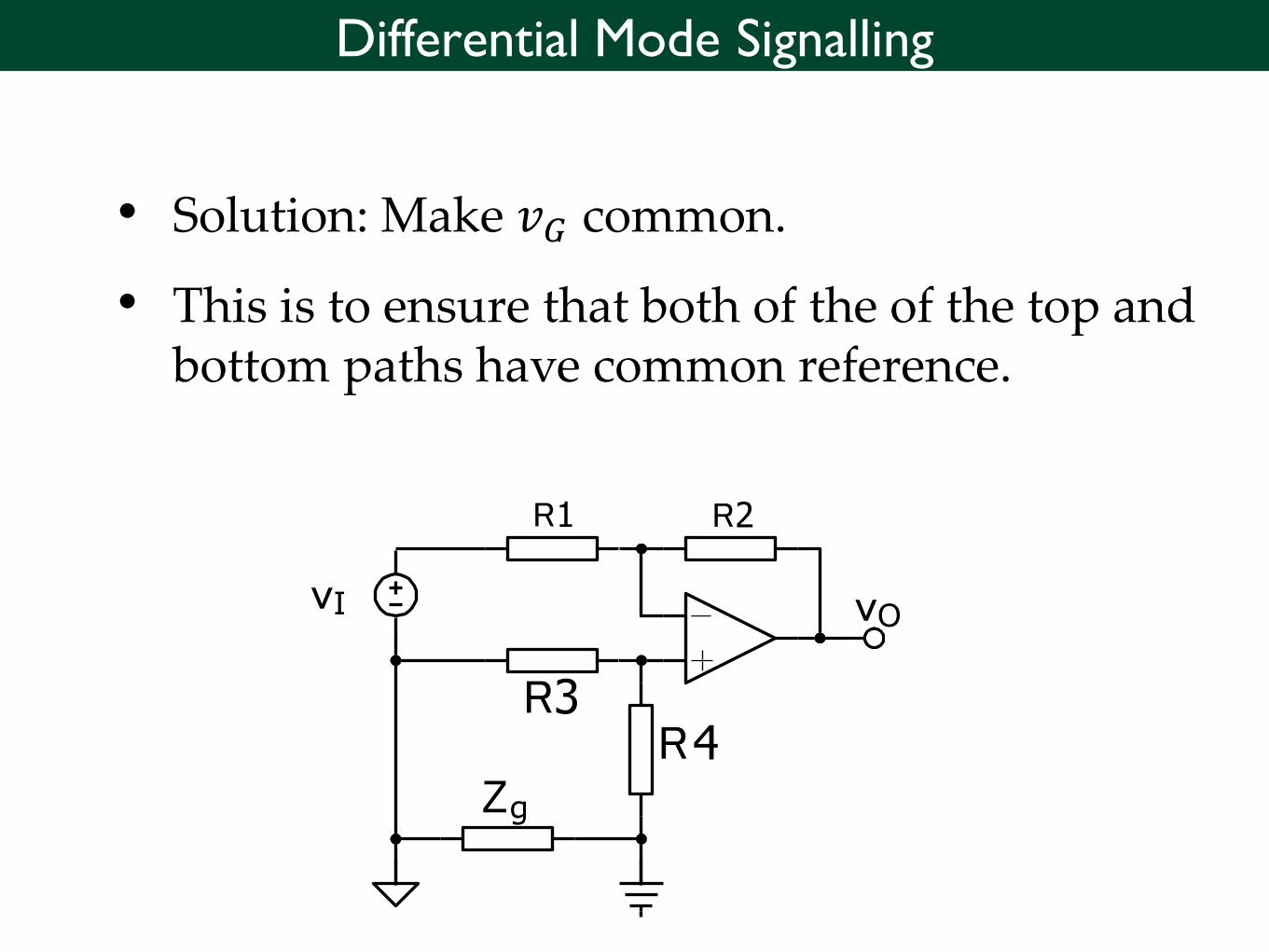
Differential Mode Signalling
• Solution: Make 𝑣𝐺 common.
• This is to ensure that both of the of the top and bottom paths have common reference.
vOvI
R3R4
Zg
R1 R2

Differential Mode Signalling
Problem: Ground loop
• As source and amplifier are often far apart – voltage drop due to ground bus impedance
vO
Zg
vI
R 1 R 2
Differential Mode Signalling
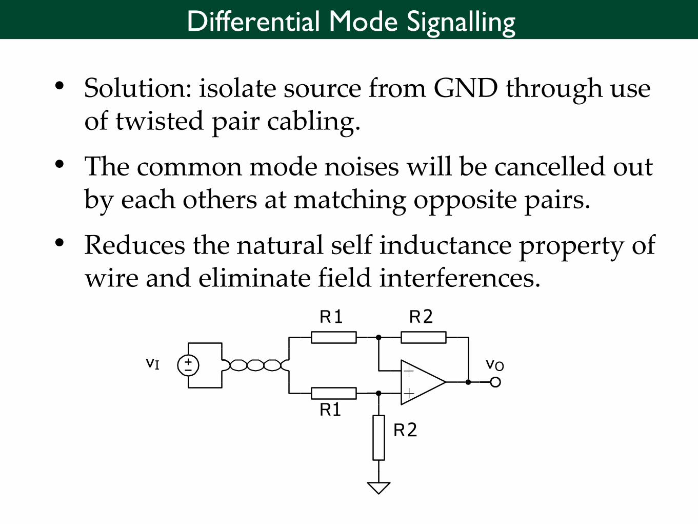
• Solution: isolate source from GND through useof twisted pair cabling.
• The common mode noises will be cancelled out by each others at matching opposite pairs.
• Reduces the natural self inductance property of wire and eliminate field interferences.
R1 R2
vO
R1R2
vI
Differential Mode Signalling
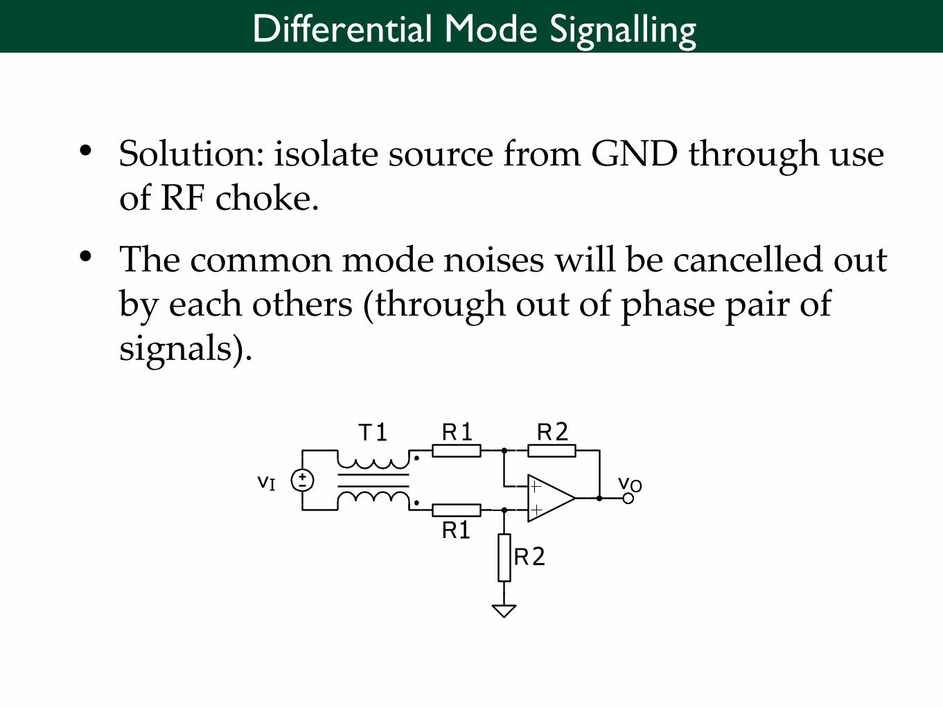
• Solution: isolate source from GND through useof RF choke.
• The common mode noises will be cancelled out by each others (through out of phase pair of signals).
R1 R2
vO
R1R2
vI
T1
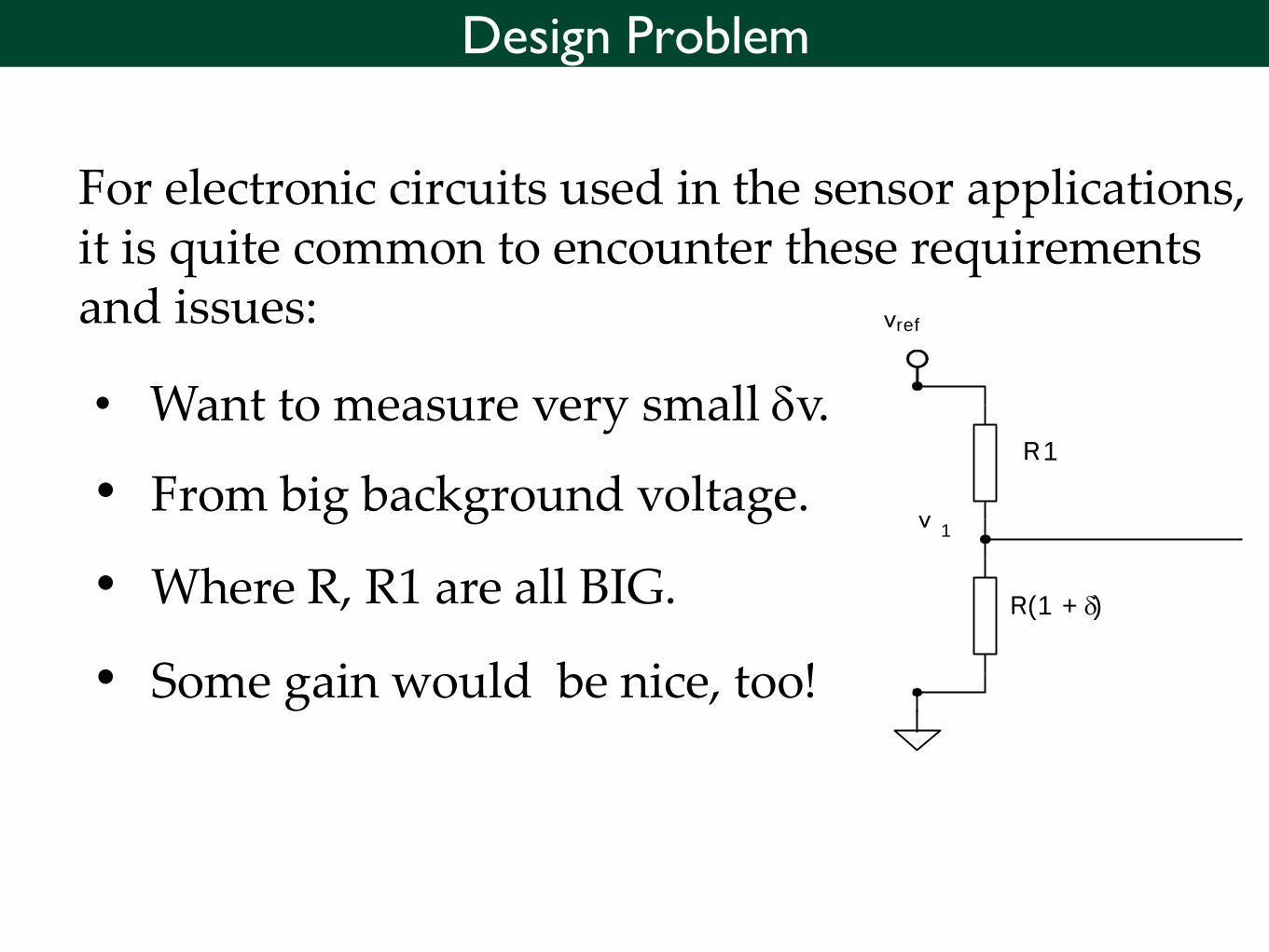
Design Problem
vref
R1
R(1 + )
v1
• Want to measure very small v.
• From big background voltage.
• Where R, R1 are all BIG.
• Some gain would be nice, too!
For electronic circuits used in the sensor applications, it is quite common to encounter these requirements and issues:
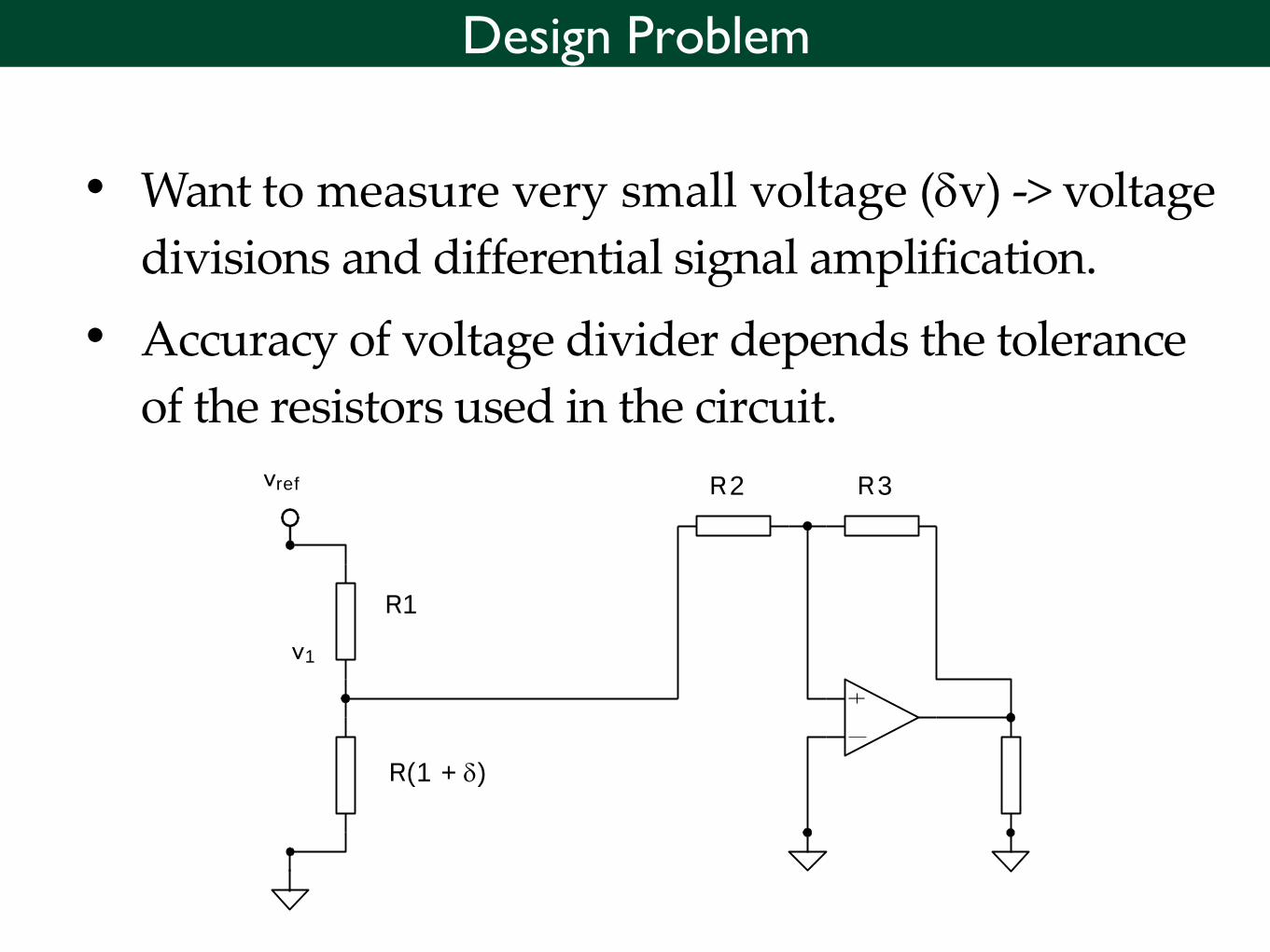
• Want to measure very small voltage (v) -> voltage
divisions and differential signal amplification.
• Accuracy of voltage divider depends the tolerance
of the resistors used in the circuit.
vref
R1
v1
R(1 + )
R3R2
Design Problem
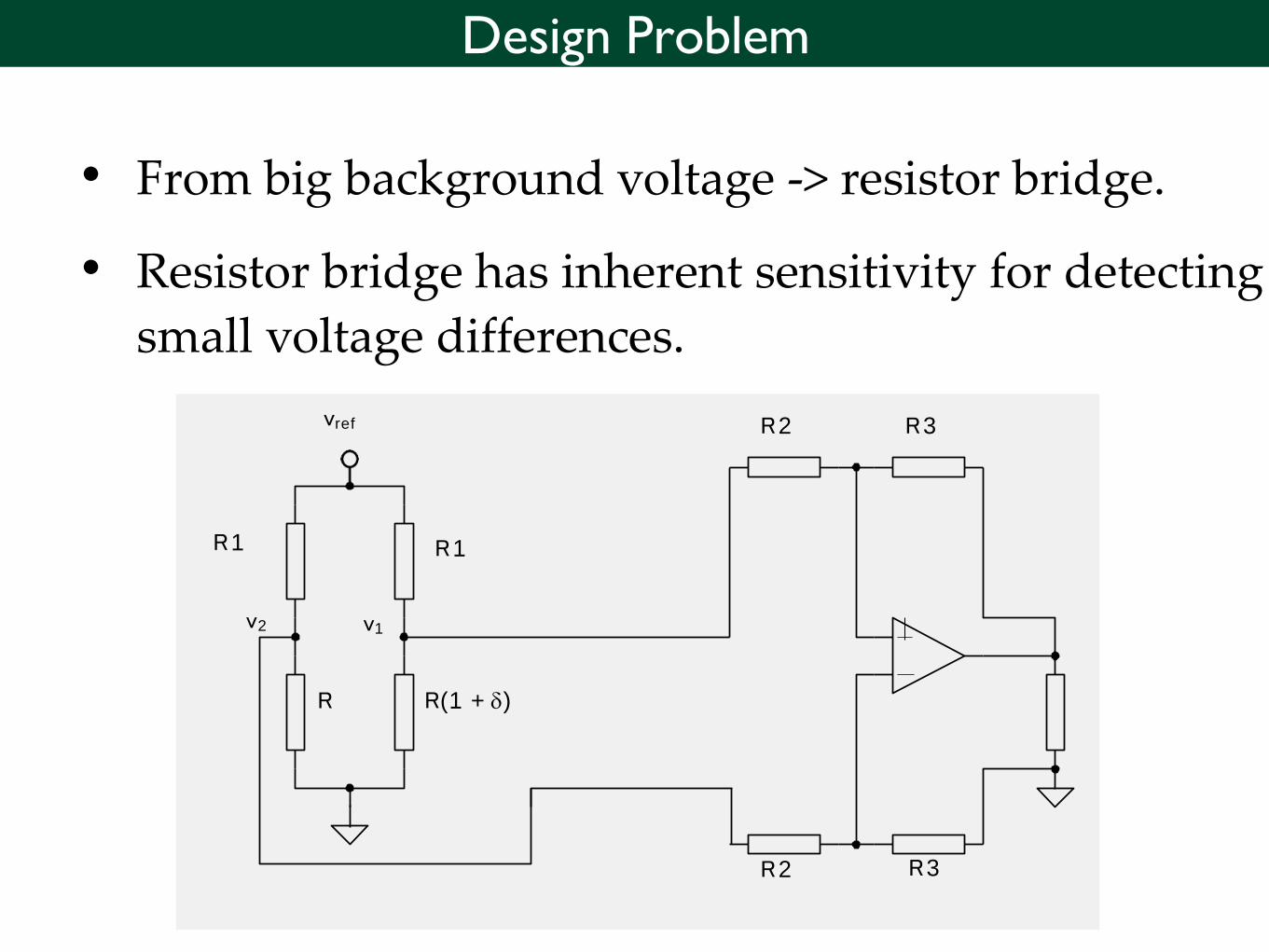
• From big background voltage -> resistor bridge.
• Resistor bridge has inherent sensitivity for detecting
small voltage differences.
vref
R1
R R(1 + )
R1
v2 v1
R3
R3R2
R2
Design Problem
vref
R1
R R(1 + )
R1
v2 v1
R2 R3
v1
R3R2v2
R4
R4
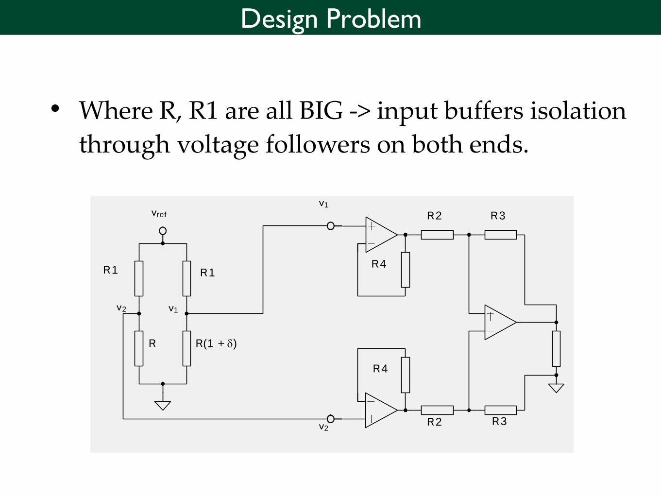
• Where R, R1 are all BIG -> input buffers isolation
through voltage followers on both ends.
Design Problem
Design Problem
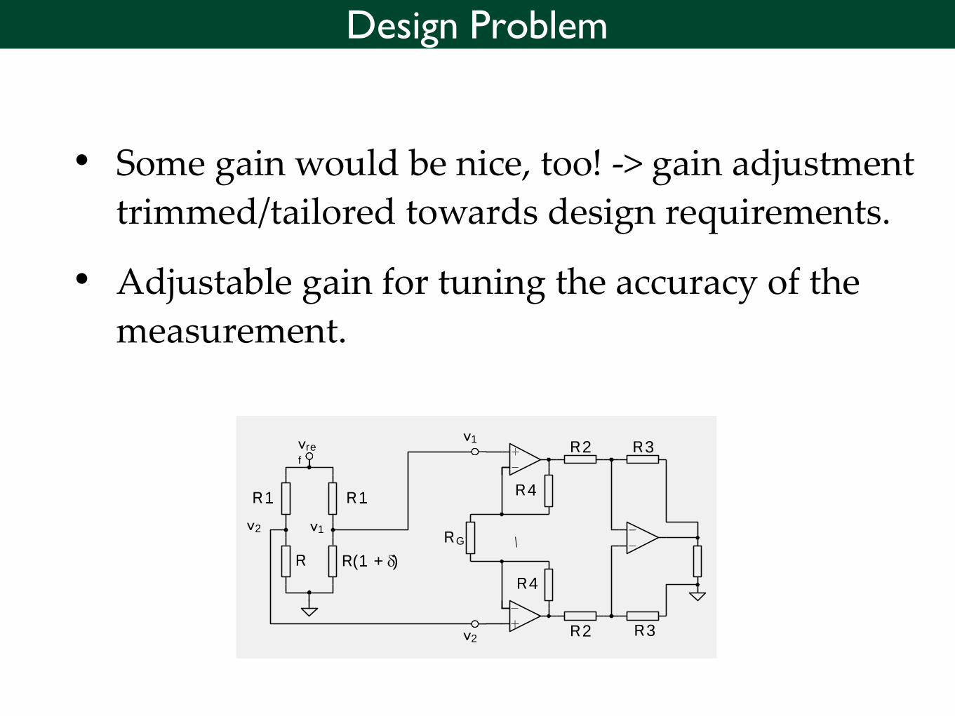
• Some gain would be nice, too! -> gain adjustment
trimmed/tailored towards design requirements.
• Adjustable gain for tuning the accuracy of the
measurement.
vref
R1
R R(1 + )
R1
v2 v1
R2 R3v1
R3R2v2
R4
RG
R4
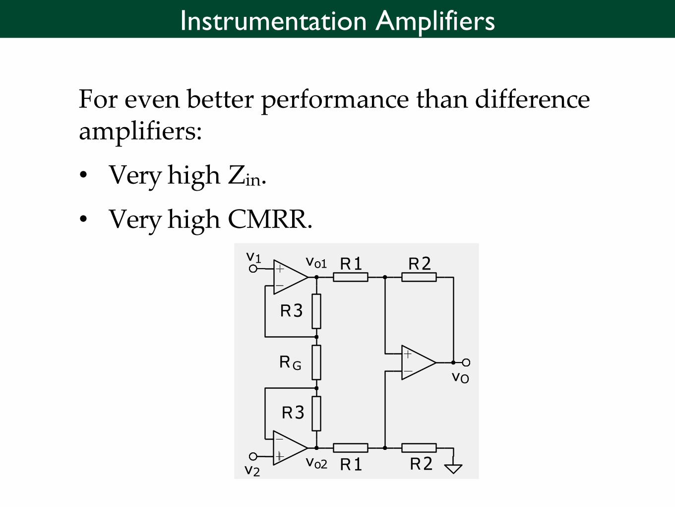
Instrumentation Amplifiers
For even better performance than differenceamplifiers:
• Very high Zin.
• Very high CMRR.
R1 R2
vO
v1
R2R1v2
R3
RG
R3
vo2
vo1
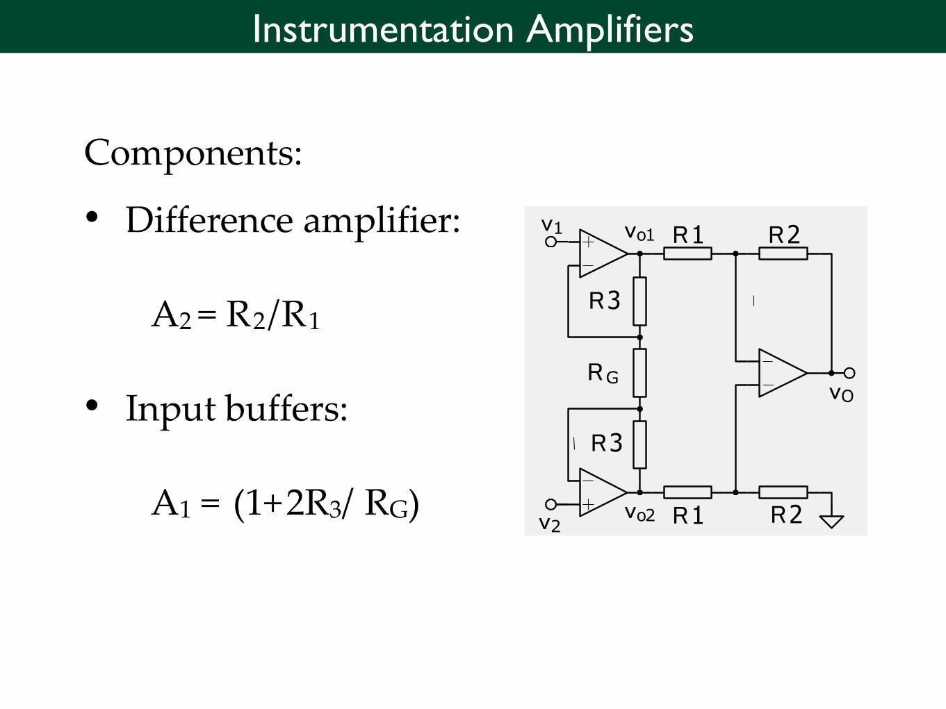
Instrumentation Amplifiers
Components:
• Difference amplifier:
A2 = R2/R1
• Input buffers:
A1 = (1+2R3/ RG)
R1 R2
vO
v1
R2R1v2
R3
RG
R3
vo2
vo1
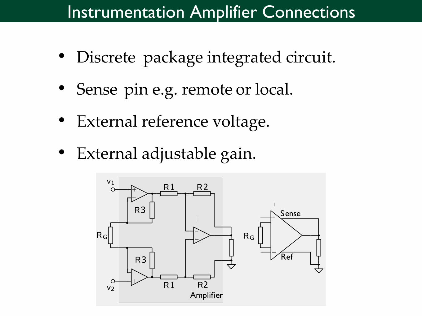
Instrumentation Amplifier Connections
• Discrete package integrated circuit.
• Sense pin e.g. remote or local.
• External reference voltage.
• External adjustable gain.
RG
Sense
Ref
R1 R2v1
R1v2
R3
RG
R3
R2Amplifier
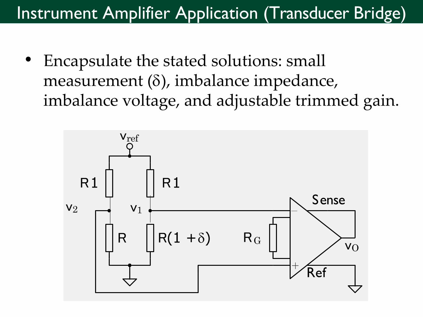
Instrument Amplifier Application (Transducer Bridge)
• Encapsulate the stated solutions: small measurement (), imbalance impedance, imbalance voltage, and adjustable trimmed gain.
vO
vref
R1
RG
Sense
Ref
R1
R R(1 +)
v2 v1
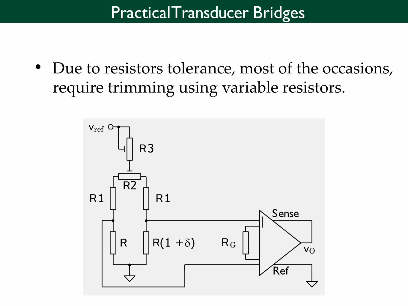
PracticalTransducer Bridges
• Due to resistors tolerance, most of the occasions, require trimming using variable resistors.
vref
R3
R2
vO
R1
RG
Sense
Ref
R1
R R(1 +)
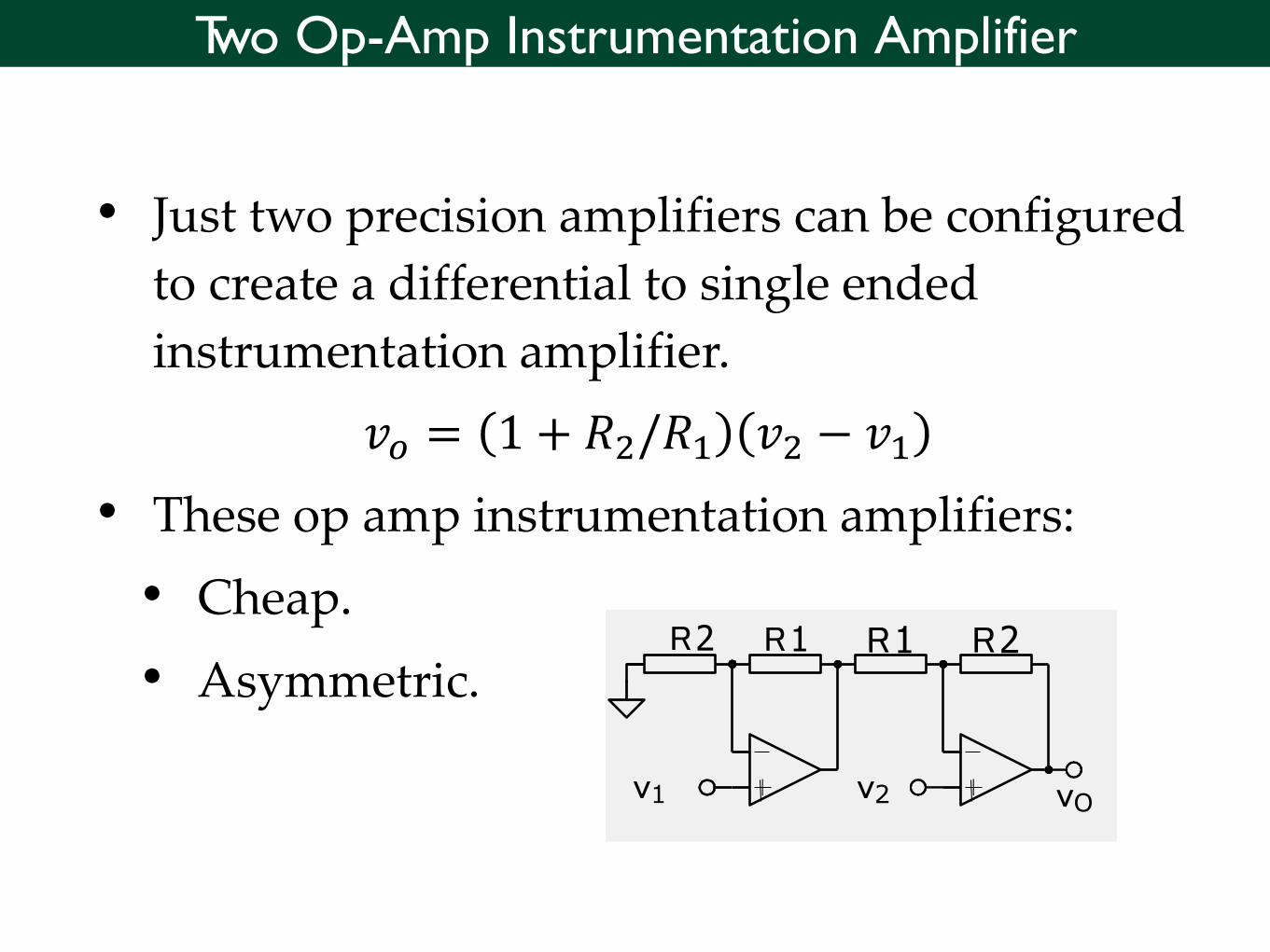
Two Op-Amp Instrumentation Amplifier
• Just two precision amplifiers can be configured
to create a differential to single ended
instrumentation amplifier.
𝑣𝑜 = 1 + 𝑅2/𝑅1 𝑣2 − 𝑣1
• These op amp instrumentation amplifiers:
• Cheap.
• Asymmetric.
v1 v2
R1 R2
vO
R1R2
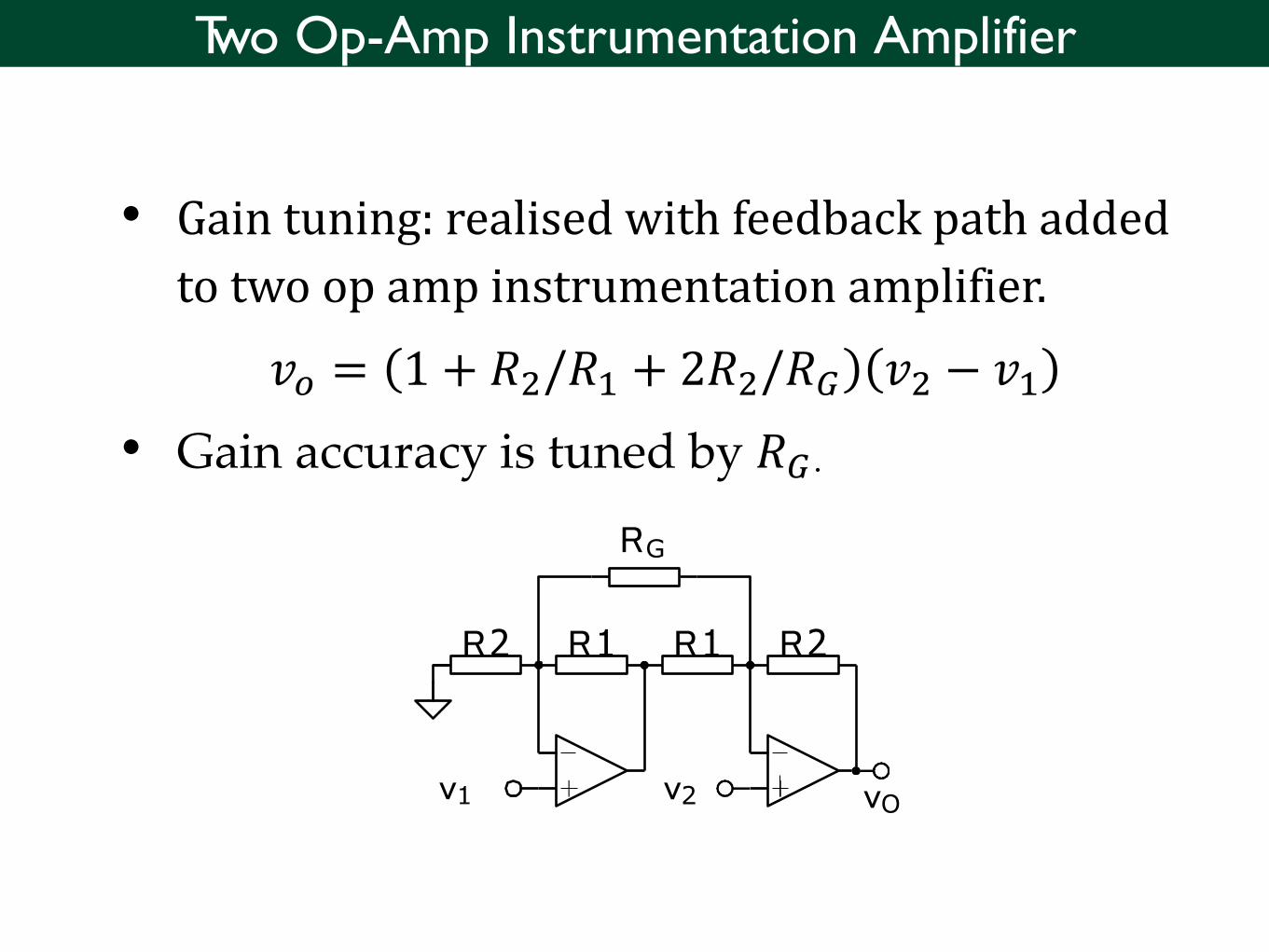
Two Op-Amp Instrumentation Amplifier
• Gain tuning: realised with feedback path added
to two op amp instrumentation amplifier.
𝑣𝑜 = 1 + 𝑅2/𝑅1 + 2𝑅2/𝑅𝐺 𝑣2 − 𝑣1
• Gain accuracy is tuned by 𝑅𝐺 .
v1 v2 vO
RG
R2 R1 R1 R2
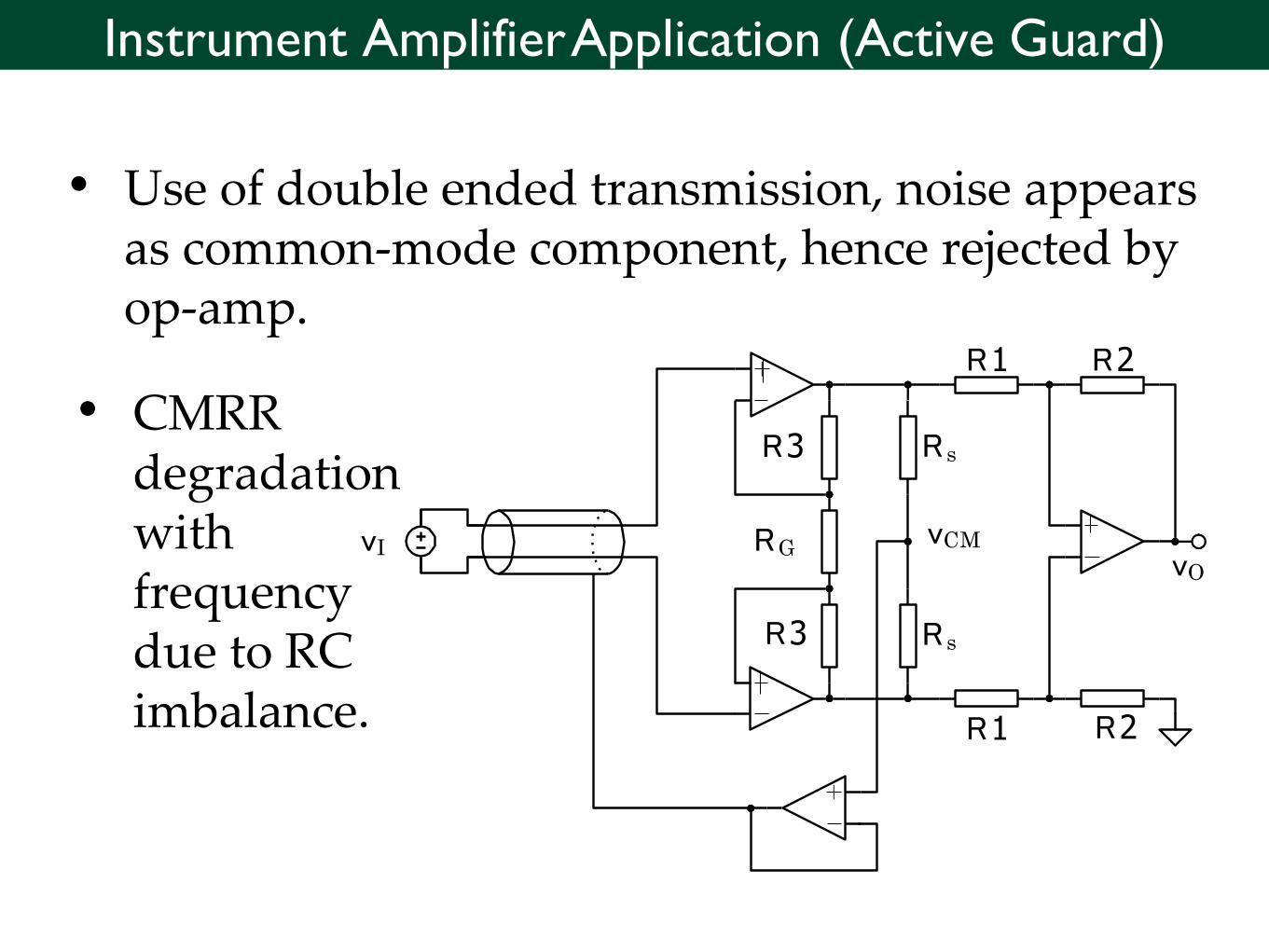
Instrument AmplifierApplication (Active Guard)
• Use of double ended transmission, noise appears as common-mode component, hence rejected by op-amp.
• CMRR degradation with frequency due to RC imbalance.
R1 R2
vO
R2R1
R3
RG
R3 R s
R s
vI vCM