Embed Size (px)
Citation preview

XMUT303 Analogue Electronics
Tutorial 5: Power Amplifier (Answer)
A. Power Amplifiers
1. For classes of power amplifier circuits given below, describe each of the power amplifier classes
in terms of their circuits, output signals with regard to input signals and Q-point biasing
requirements of the transistor.
a. Class A
b. Class B
c. Class AB
d. Class C
e. Class D
Answer
a. In the Class A amplifier, the output signal varies for a full 360° of the input signal. Class A
power amplifier requires the Q -point to be biased at a level so that at least half the signal
swing of the output may vary up and down without going to a high enough voltage to be
limited by the supply voltage level or too low to approach the lower supply level, or 0 V.
b. In the Class B amplifier, it provides an output signal varying over one-half the input signal
cycle, or for 180° of signal. For Class B amplifier, the dc bias point for Class B is at 0 V, with
the output then varying from this bias point for a half-cycle. Obviously, the output is not a
faithful reproduction of the input if only one half-cycle is present. Two Class B operations—

XMUT303 Analogue Electronics Tutorial 5: Power Amplifiers (Answer)
School of Engineering and Computer Science VUW/XMUT 2
one to provide output on the positive-output half-cycle and another to provide operation on
the negative-output half-cycle—are necessary.
c. For Class AB operation, the output signal swing occurs between 180° and 360° and is neither
Class A nor Class B operation. Class AB amplifier may be biased at a dc level above the zero-
base-current level of class B and above one-half the supply voltage level of Class A (e.g. this
bias condition is Class AB). Class AB operation still requires a push–pull connection to
achieve a full output cycle, but the dc bias level is usually closer to the zero-base-current
level for better power efficiency.
d. The output of a Class C amplifier is biased for operation at less than 180° of the cycle and will
operate only with a tuned (resonant) circuit, which provides a full cycle of operation for the
tuned or resonant frequency. In the Class C amplifier, Q-point for the biasing is determined
at negative emitter current of the transistor. Since it is designed for a tuned/resonant
condition, the operation of this class of amplifier is therefore used in special areas of tuned
circuits, such as circuits in the radio or communications.
XMUT303 Analogue Electronics Tutorial 5: Power Amplifiers (Answer)
School of Engineering and Computer Science VUW/XMUT 3
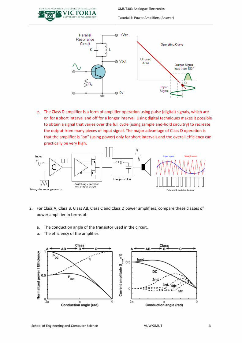
e. The Class D amplifier is a form of amplifier operation using pulse (digital) signals, which are
on for a short interval and off for a longer interval. Using digital techniques makes it possible
to obtain a signal that varies over the full cycle (using sample and-hold circuitry) to recreate
the output from many pieces of input signal. The major advantage of Class D operation is
that the amplifier is “on” (using power) only for short intervals and the overall efficiency can
practically be very high.
2. For Class A, Class B, Class AB, Class C and Class D power amplifiers, compare these classes of
power amplifier in terms of:
a. The conduction angle of the transistor used in the circuit.
b. The efficiency of the amplifier.

XMUT303 Analogue Electronics Tutorial 5: Power Amplifiers (Answer)
School of Engineering and Computer Science VUW/XMUT 4
Answer
For the stated classes of power amplifier, compare their differences.
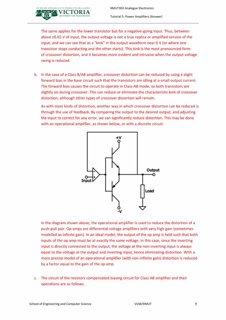
a. As far as the conduction angle is concerned, Class A amplifier has full cycle 360° of
conduction whereas Class B amplifier has half cycle 180° of conduction.
This is in contrast with the Class AB amplifier that has slightly more than 180° of conduction
and the Class C amplifier has slightly less than 180° of conduction.
Furthermore, Class D amplifier is an ON-OFF non-linear switching type of power amplifier.
Amplifier Class Description Conduction Angle
Class A Full cycle 360° of Conduction θ = 2π
Class B Half cycle 180° of Conduction θ = π
Class AB Slightly more than 180° of conduction π < θ < 2π
Class C Slightly less than 180° of conduction θ < π
Class D ON-OFF non-linear switching θ = 0
b. The power efficiency of an amplifier, defined as the ratio of power output to power input,
improves (gets higher) going from Class A to Class D.
Class A amplifier, with dc bias at one-half the supply voltage level, uses a good amount of
power to maintain bias, even with no input signal applied. This results in very poor
efficiency, especially with small input signals, when very little ac power is delivered to the
load. In fact, the maximum efficiency of a Class A circuit, occurring for the largest output

XMUT303 Analogue Electronics Tutorial 5: Power Amplifiers (Answer)
School of Engineering and Computer Science VUW/XMUT 5
voltage and current swing, is only 25% with a direct or series-fed load connection and 50%
with a transformer connection to the load.
Class B operation, with no dc bias power for no input signal, can be shown to provide a
maximum efficiency that reaches 78.5%.
Since Class AB falls between Class A and Class B in bias, it also falls between their efficiency
ratings—between 25% (or 50%) and 78.5%.
Class C/D operation can achieve power efficiency over 90% and provides the most efficient
operation of all the operating classes.
B. Class A Amplifier
3. For a Class A power amplifier circuit in the figure given below, it has an input voltage that results
in a base current of 10 mA peak. Calculate the following:
a. 𝑄-point of the biasing circuit of the amplifier.
b. Input power of the amplifier.
c. Output power of the amplifier.
d. Efficiency of the amplifier.
Answer
a. Using relevant equation for the given transistor, we can determine the 𝑄 -point to be as
follows.
The quotient current at the base of the transistor:
𝐼𝐵𝑄=
𝑉𝐶𝐶 − 0.7 V
𝑅𝐵=
20 V − 0.7 V
1 k= 19.3 mA
The quotient current at the collector of the transistor:
𝐼𝐶𝑄= 𝛽𝐼𝐵 = (25)(19.3 mA) = 0.4825 A

XMUT303 Analogue Electronics Tutorial 5: Power Amplifiers (Answer)
School of Engineering and Computer Science VUW/XMUT 6
The quotient voltage across the collector-emitter of the transistor:
𝑉𝐶𝐸𝑄= 𝑉𝐶𝐶 − 𝐼𝐶𝑅𝐶 = 20 V − (0.4825 A)(20 ) = 10.4 V
This bias point is marked on the transistor collector characteristic of figure given below.
The ac variation of the output signal can be obtained graphically using the dc load line drawn
on the graph by connecting 𝑉𝐶𝐸 = 𝑉𝐶𝐶 = 20 V with 𝐼𝐶 = 𝑉𝐶𝐶/𝑅𝐶 = 1000 mA = 1 A, as
shown in the graph above.
b. Using equation for input power results, the input power of the amplifier is:
𝑃𝐼(𝑑𝑐) = 𝑉𝐶𝐶𝐼𝐶𝑄= (20 V)(0.4825 A) = 9.6 W
c. When the input ac base current increases from its dc bias level, the collector current rises
by:
𝐼𝐶(𝑝) = 𝛽𝐼𝐵(𝑝) = (25)(10 mA peak) = 250 mA peak
Using the equation for the output power of the amplifier yields:
𝑃𝑂(𝑎𝑐) = 𝐼𝐶2(𝑟𝑚𝑠)𝑅𝐶 =
𝐼𝐶2
2𝑅𝐶 =
(250 × 10−3A)2
2(20 ) = 0.625 W
d. The amplifier’s power efficiency can then be calculated using the equation for calculating
efficiency:
% 𝜂 =𝑃𝑂(𝑎𝑐)
𝑃𝐼(𝑑𝑐)× 100% =
0.625 W
9.6 W× 100% = 6.5%

XMUT303 Analogue Electronics Tutorial 5: Power Amplifiers (Answer)
School of Engineering and Computer Science VUW/XMUT 7
C. Class B Amplifiers
4. For a Class B power amplifier providing a 20-V peak signal to a 16- load (speaker) and a power
supply of 𝑉𝐶𝐶 = 30 V, determine:
a. The input power of the amplifier.
b. The output power of the amplifier.
c. The circuit efficiency of the amplifier.
Answer
a. A 20-V peak signal across a 16- load provides a peak load current of:
𝐼𝐿(𝑝) =𝑉𝐿(𝑝)
𝑅𝐿=
20 V
16 = 1.25 A
The dc value of the current drawn from the power supply is then:
𝐼𝑑𝑐 = (2
𝜋) 𝐼𝐿(𝑝) = (
2
𝜋) (1.25 A) = 0.796 A
The input power delivered by the supply voltage is:
𝑃𝐼(𝑑𝑐) = 𝑉𝐶𝐶𝐼𝑑𝑐 = (30 V)(0.796 A) = 23.9 W
b. The output power delivered to the load is:
𝑃𝑂(𝑎𝑐) =𝑉𝐿
2(𝑝)
2𝑅𝐿=
(20 V)2
2(16 )= 12.5 W
c. This yields a resulting efficiency of:
% 𝜂 = [𝑃𝑂(𝑎𝑐)
𝑃𝐼(𝑑𝑐)] × 100% = [
12.5 W
23.9 W] × 100% = 52.3%
5. Class AB power amplifier or push-pull Class B power amplifier introduces some improvement
towards design of Class B power amplifier.
a. Describe the crossover distortion problem which is typically associated with the operation of
Class AB amplifier.
b. Describe op amp feedback improvement introduced of the Class AB amplifier for eliminating
the crossover distortion.
c. Describe the circuit and operations of the resistors compensated biasing for the Class AB
amplifier circuit.
d. Describe the circuit and operations of the diodes compensated biasing for the Class AB
amplifier circuit.

XMUT303 Analogue Electronics Tutorial 5: Power Amplifiers (Answer)
School of Engineering and Computer Science VUW/XMUT 8
Answer
a. Crossover distortion problem in Class AB amplifier is a type of distortion which is caused by
switching between devices driving a load. It is most commonly seen in complementary, or
"push-pull", Class-B amplifier stages, although it is occasionally seen in other types of circuits
as well. The term crossover signifies the "crossing over" of the signal between devices, in this
case, from the upper transistor to the lower and vice versa.
The diagram above shows a typical class-B emitter-follower complementary output stage.
Under no signal conditions, the output is exactly midway between the supplies (i.e., at 0 V).
When this is the case, the base-emitter bias of both the transistors is zero, so they are in the
cut-off region where the transistors are not conducting.
Consider a positive-going swing: As long as the input is less than the required forward
VBE drop (≈ 0.65 V) of the upper NPN transistor, it will remain off or conduct very little - this
is the same as a diode operation as far as the base circuit is concerned, and the output
voltage does not follow the input (the lower PNP transistor is still off because its base-
emitter diode is being reverse biased by the positive-going input).
XMUT303 Analogue Electronics Tutorial 5: Power Amplifiers (Answer)
School of Engineering and Computer Science VUW/XMUT 9
The same applies for the lower transistor but for a negative-going input. Thus, between
about ±0.65 V of input, the output voltage is not a true replica or amplified version of the
input, and we can see that as a "kink" in the output waveform near 0 V (or where one
transistor stops conducting and the other starts). This kink is the most pronounced form
of crossover distortion, and it becomes more evident and intrusive when the output voltage
swing is reduced.
b. In the case of a Class B/AB amplifier, crossover distortion can be reduced by using a slight
forward bias in the base circuit such that the transistors are idling at a small output current.
The forward bias causes the circuit to operate in Class-AB mode, so both transistors are
slightly on during crossover. This can reduce or eliminate the characteristic kink of crossover
distortion, although other types of crossover distortion will remain.
As with most kinds of distortion, another way in which crossover distortion can be reduced is
through the use of feedback. By comparing the output to the desired output, and adjusting
the input to correct for any error, we can significantly reduce distortion. This may be done
with an operational amplifier, as shown below, or with a discrete circuit.
In the diagram shown above, the operational amplifier is used to reduce the distortion of a
push-pull pair. Op-amps are differential voltage amplifiers with very high gain (sometimes
modelled as infinite gain). In an ideal model, the output of the op amp is held such that both
inputs of the op amp must be at exactly the same voltage. In this case, since the inverting
input is directly connected to the output, the voltage at the non-inverting input is always
equal to the voltage at the output and inverting input, hence eliminating distortion. With a
more precise model of an operational amplifier (with non-infinite gain) distortion is reduced
by a factor equal to the gain of the op amp.
c. The circuit of the resistors compensated biasing circuit for Class AB amplifier and their
operations are as follows.

XMUT303 Analogue Electronics Tutorial 5: Power Amplifiers (Answer)
School of Engineering and Computer Science VUW/XMUT 10
An adjustable resistor, or potentiometer can be used to bias both transistors onto the verge
of conduction. Then transistors TR1 and TR2 are biased via RB1-VR1-RB2 so that their outputs
are balanced and zero quiescent current flows into the load.
The input signal which is applied via capacitors C1 and C2 is superimposed onto the biasing
voltages and applied to the bases of both transistors. Note that both the signals applied to
each base has the same frequency and amplitude as they originated from VIN.
The advantage of this adjustable biasing arrangement is that the basic amplifier circuit does
not require the use of complimentary transistors with closely matched electrical
characteristics or an exact resistor ratio within the voltage divider network as the
potentiometer can be adjusted to compensate.
As resistors are passive devices that convert electrical power into heat due to its power
rating, the resistive biasing of a Class AB amplifier, either fixed or adjustable, can be very
sensitive to changes in temperature. Any small changes in the operating temperature of the
biasing resistors (or transistors) may affect their value producing undesirable changes in the
quiescent collector current of each transistor.
One way to overcome this temperature related problem is to replace the resistors with
diodes to use diode biasing.
d. The circuit of the diode compensated biasing circuit for Class AB amplifier and their
operations are as follows.
While the use of biasing resistors may not solve the temperature problem, one way to
compensate for any temperature related variation in the base-emitter voltage, (VBE) is to use
a pair of normal forward biased diodes within the amplifiers biasing arrangement as shown
below.

XMUT303 Analogue Electronics Tutorial 5: Power Amplifiers (Answer)
School of Engineering and Computer Science VUW/XMUT 11
A small constant current flows through the series circuit of R1-D1-D2-R2, producing voltage
drops which are symmetrical either side of the input. With no input signal voltage applied,
the point between the two diodes is zero volts. As current flows through the chain, there is a
forward bias voltage drop of approximately 0.7 V across the diodes which is applied to the
base-emitter junctions of the switching transistors.
Therefore the voltage drop across the diodes, biases the base of transistor TR1 to about 0.7
volts, and the base of transistor TR2 to about –0.7 Volts. Thus, the two silicon diodes provide
a constant voltage drop of approximately 1.4 Volts between the two bases biasing them
above cut-off.
As the temperature of the circuit rises, so too does that of the diodes as they are located
next to the transistors. The voltage across the PN junction of the diode thus decreases
diverting some of the transistors base current stabilising the transistors collector current.
If the electrical characteristics of the diodes are closely matched to that of the transistors
base-emitter junction, the current flowing in the diodes and the current in the transistors
will be the same creating what is called a current mirror. The effect of this current mirror
compensates for variations in temperature producing the required Class AB operation
thereby eliminating any crossover distortion.
6. For a Class AB power amplifier circuit as shown in the figure below, assume that the circuit is a
preamplifier stage with an output signal voltage of 3 V rms and an output resistance of 50 is
driving the push-pull power amplifier. Transistors 𝑄1 and 𝑄2 in the power amplifier have a 𝛽𝑎𝑐 of
100 and an 𝑟𝑒′ of 1.6 .

XMUT303 Analogue Electronics Tutorial 5: Power Amplifiers (Answer)
School of Engineering and Computer Science VUW/XMUT 12
a. Determine the maximum ideal peak values for the output voltage and current of the
amplifier.
b. Find the maximum ac output power and the dc input power of the amplifier.
c. Determine the loading effect that the power amplifier has on the preamp stage.
Answer
a. For the given Class AB amplifier, the ideal maximum peak output voltage is:
𝑉𝑜𝑢𝑡(𝑝𝑒𝑎𝑘) ≅ 𝑉𝐶𝐸𝑄 =𝑉𝐶𝐶
2=
20 V
2= 10 V
The maximum peak output current is:
𝐼𝑜𝑢𝑡(𝑝𝑒𝑎𝑘) ≅ 𝐼𝐶(𝑠𝑎𝑡) =𝑉𝐶𝐸𝑄
𝑅𝐿=
10 V
8 = 1.25 A
b. For calculation of the ac output and the dc output powers,
The ac output power is:
𝑃𝑜𝑢𝑡 = 0.25𝐼𝐶(𝑠𝑎𝑡)𝑉𝐶𝐶 = 0.25(1.25 A)(20 V) = 6.25 W
The dc output power is:
𝑃𝐷𝐶 =𝐼𝐶(𝑠𝑎𝑡)𝑉𝐶𝐶
𝜋=
(1.25 A)(20 V)
𝜋= 7.96 W
c. Looking from the input signal source, the bias resistors appear in parallel because both go to
ac ground and the ac resistance of the forward-biased diodes is very small and can be
ignored.

XMUT303 Analogue Electronics Tutorial 5: Power Amplifiers (Answer)
School of Engineering and Computer Science VUW/XMUT 13
The input resistance at the emitter of either transistor is:
𝛽𝑎𝑐(𝑟𝑒′ + 𝑅𝐿)
So, the signal source sees 𝑅1, 𝑅2, and 𝛽𝑎𝑐(𝑟𝑒′ + 𝑅𝐿) all in parallel. The ac input resistance of
the power amplifier is:
𝑅𝑖𝑛 = 𝛽𝑎𝑐(𝑟𝑒′ + 𝑅𝐿) ∥ 𝑅1 ∥ 𝑅2 = 100(1.6 + 8 )||470 ||470 = 188
Obviously, this will have an effect on the preamp driver stage.
The output resistance of the preamp stage and the input resistance of the power amp
effectively form a voltage divider that reduces the output signal from the preamp.
The actual signal at the power amp is:
𝑉𝑖𝑛 = (𝑅𝑖𝑛
𝑅𝑠 + 𝑅𝑖𝑛) 𝑉𝑠 = (
188
50 + 188 ) (3 V) = 2.37 V
D. Class C Amplifier
7. For a given Class C power amplifier circuit as shown in the figure below, it is realised as a
common-emitter amplifier with a resistive load.
a. Describe basic operation of the amplifier.
b. Describe power dissipation of the amplifier.
c. State expressions that describe the power dissipation of the amplifier.
Answer
a. A Class C amplifier is normally operated with a resonant circuit load, so the resistive load is
used only for the purpose of illustrating the concept. It is biased below cut-off with the
negative VBB supply.
The ac source voltage has a peak value that is slightly greater than |Vbb| + Vbe so that the
base voltage exceeds the barrier potential of the base-emitter junction for a short time near
the positive peak of each cycle, as illustrated in the figure given below.

XMUT303 Analogue Electronics Tutorial 5: Power Amplifiers (Answer)
School of Engineering and Computer Science VUW/XMUT 14
During this short interval, the transistor is turned on. When the entire ac load line is used, as
shown in the figure below, the ideal maximum collector current is Ic(sat), and the ideal
minimum collector voltage is Vce(sat).
b. The power dissipation of the transistor in a Class C amplifier is low because it is on for only a
small percentage of the input cycle. Figure below shows the collector current pulses.
The time between the pulses is the period (T) of the ac input voltage. The collector current
and the collector voltage during the on time of the transistor are shown in the figure given
below.

XMUT303 Analogue Electronics Tutorial 5: Power Amplifiers (Answer)
School of Engineering and Computer Science VUW/XMUT 15
c. To avoid complex mathematics, we will assume ideal pulse approximations.
Using this simplification, if the output swings over the entire load, the maximum current
amplitude is Ic(sat) and the minimum voltage amplitude is Vce(sat) during the time the
transistor is on.
The power dissipation during the on time is, therefore:
𝑃𝐷(𝑜𝑛) = 𝐼𝐶(𝑠𝑎𝑡)𝑉𝐶𝐸(𝑠𝑎𝑡)
The transistor is on for a short time, ton, and off for the rest of the input cycle. Therefore,
assuming the entire load line is used, the power dissipation averaged over the entire cycle is:
𝑃𝐷(𝑎𝑣𝑒) = (𝑡𝑜𝑛
𝑇) 𝑃𝐷(𝑜𝑛) = (
𝑡𝑜𝑛
𝑇) 𝐼𝐶(𝑠𝑎𝑡)𝑉𝐶𝐸(𝑠𝑎𝑡)
8. A Class C power amplifier is driven by a 200 kHz signal. The transistor is on for 1 ms, and the
amplifier is operating over 100 percent of its load line.
a. If 𝐼𝑐(𝑠𝑎𝑡) = 100 mA and𝑉𝐶𝐸(𝑠𝑎𝑡) = 0.2 V, what is the average power dissipation of the
transistor in the circuit?
b. Suppose the Class C amplifier described in part (a) has a 𝑉𝐶𝐶 equal to 24 V and the resistor
𝑅𝐶 is 100 . Determine the efficiency of the amplifier circuit.
Answer
a. For the given Class C amplifier, the period of conduction is given as:
𝑇 =1
𝑓𝑠=
1
200 kHz= 5 μs
Therefore, the average power dissipation of the amplifier is:
𝑃𝐷(𝑎𝑣𝑒) = (𝑡𝑜𝑛
𝑇) 𝐼𝐶(𝑠𝑎𝑡)𝑉𝐶𝐸(𝑠𝑎𝑡) = (0.2)(100 mA)(0.2 V) = 4 mW

XMUT303 Analogue Electronics Tutorial 5: Power Amplifiers (Answer)
School of Engineering and Computer Science VUW/XMUT 16
The low power dissipation of the transistor operated in Class C is important because, as you
will see later, it leads to a very high efficiency when it is operated as a tuned Class C
amplifier in which relatively high power is achieved in the resonant circuit.
b. For the given Class C amplifier, from part (a), we know that the average power dissipation,
𝑃𝐷(𝑎𝑣𝑒) = 4 mW. As a result, the output power of the amplifier is:
𝑃𝑜𝑢𝑡 =0.5𝑉𝐶𝐶
2
𝑅𝐶=
(0.5)(24 V)2
100 = 2.88 W
Therefore
𝜂 =𝑃𝑜𝑢𝑡
𝑃𝑜𝑢𝑡 + 𝑃𝐷(𝑎𝑣𝑒)=
2.88 W
2.88 W + 4 mW= 0.999
Or, as a percentage the efficiency of the amplifier is 99.9 %.
E. Class D Amplifier
9. Class-D power amplifiers work by generating a train of rectangular pulses of fixed amplitude but
varying width and separation, or varying number per unit time, representing the amplitude
variations of the analogue input signal.
a. Describe the mechanism of the operation of a Class D amplifier.
b. State the major advantage of Class D amplifier compared with other power amplifiers.
Answer
a. Class-D amplifiers work by generating a train of rectangular pulses of fixed amplitude but
varying width and separation, or varying number per unit time, representing the amplitude
variations of the analogue audio input signal.
From the diagram given below, the analogue audio input signal is modulated with a
reference triangle-wave.

XMUT303 Analogue Electronics Tutorial 5: Power Amplifiers (Answer)
School of Engineering and Computer Science VUW/XMUT 17
The output of the modulator is then used to gate the output transistors on and off
alternately.
The design of the amplifier should ensure that the pair of transistors are never allowed to
conduct together, as this would cause a short circuit between the supply rails through the
transistors.
Since the transistors are either fully "on" or fully "off", they spend very little time in the
linear region, and dissipate very little power. This is the main reason for the Class D
amplifier’s high efficiency.
In the output of the circuit, a simple low-pass filter consisting of an inductor and a capacitor
provides a path for the low frequencies of the audio signal, leaving the high-frequency
pulses behind.
b. The major advantage of a Class-D amplifier is that it can be more efficient than a linear
amplifier, with less power dissipated as heat in the active devices.
Given that large heat sinks are not required, Class-D amplifiers are also much lighter weight
than Class A, B, or AB amplifiers, an important consideration with portable electronic
devices.