Embed Size (px)
Citation preview
Lecture 22: PLLs and DLLs
22: PLLs and DLLs 2CMOS VLSI DesignCMOS VLSI Design 4th Ed.
OutlineClock System ArchitecturePhase-Locked Loops Delay-Locked Loops
22: PLLs and DLLs 3CMOS VLSI DesignCMOS VLSI Design 4th Ed.
Clock GenerationLow frequency:– Buffer input clock and drive to all registers
High frequency– Buffer delay introduces large skew relative to
input clocks• Makes it difficult to sample input data
– Distributing a very fast clock on a PCB is hard

22: PLLs and DLLs 4CMOS VLSI DesignCMOS VLSI Design 4th Ed.
Zero-Delay BufferIf the periodic clock is delayed by Tc, it is indistinguishable from the original clockBuild feedback system to guarantee this delay
Phase-Locked Loop (PLL)
Delay-Locked Loop (PLL)
22: PLLs and DLLs 5CMOS VLSI DesignCMOS VLSI Design 4th Ed.
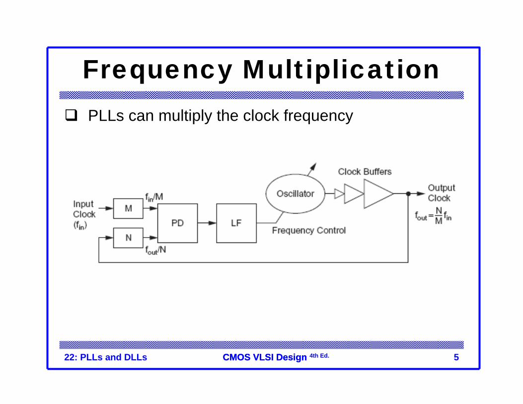
Frequency MultiplicationPLLs can multiply the clock frequency
22: PLLs and DLLs 6CMOS VLSI DesignCMOS VLSI Design 4th Ed.
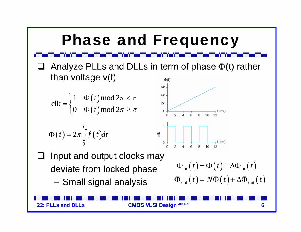
Phase and FrequencyAnalyze PLLs and DLLs in term of phase Φ(t) rather than voltage v(t)
Input and output clocks may deviate from locked phase– Small signal analysis
( )( )
1 mod 2clk
0 mod 2tt
π ππ π
Φ <⎧⎪= ⎨ Φ ≥⎪⎩
( ) ( )0
2t
t f t dtπΦ = ∫
( ) ( ) ( )( ) ( ) ( )
in in
out out
t t t
t N t t
Φ = Φ +ΔΦ
Φ = Φ + ΔΦ
22: PLLs and DLLs 7CMOS VLSI DesignCMOS VLSI Design 4th Ed.
Linear System ModelTreat PLL/DLL as a linear system– Compute deviation DF from locked position– Assume small deviations from locked– Treat system as linear for these small changes
Analysis is not valid far from lock– e.g. during acquisition at startup
Continuous time assumption– PLL/DLL is really a discrete time system
• Updates once per cycle– If the bandwidth << 1/10 clock freq, treat as continuous
Use Laplace transforms and standard analysis of linear continuous-time feedback control systems
22: PLLs and DLLs 8CMOS VLSI DesignCMOS VLSI Design 4th Ed.
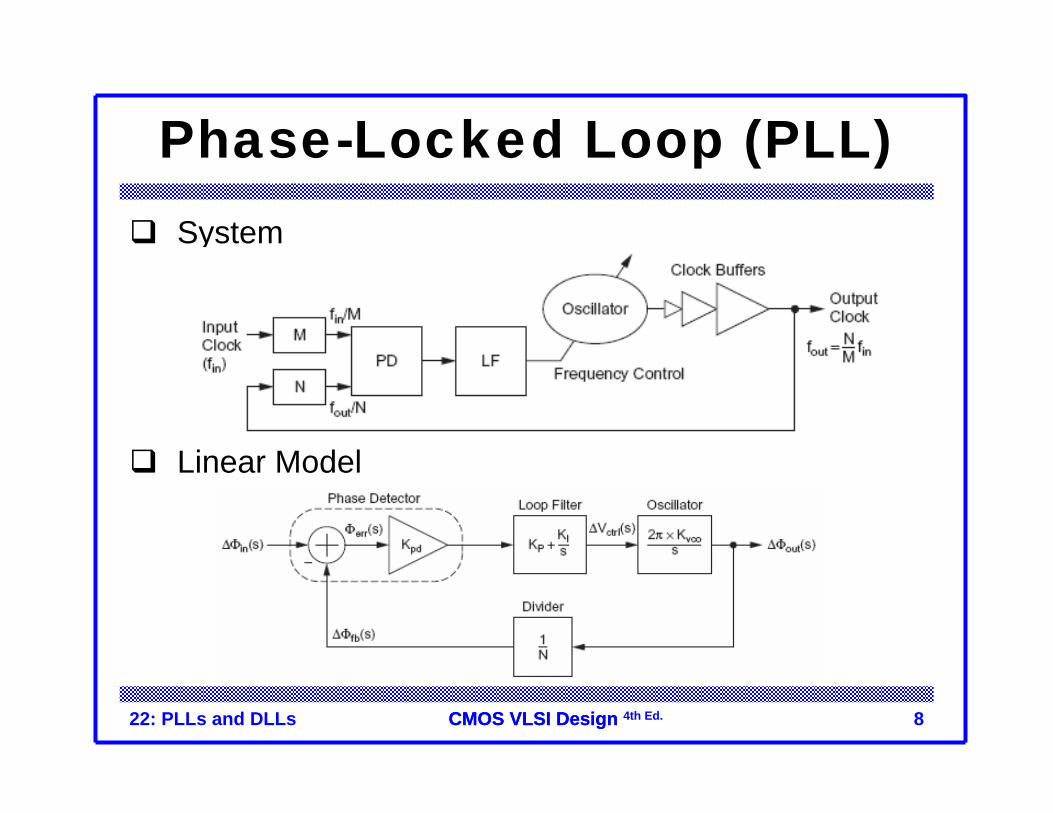
Phase-Locked Loop (PLL)System
Linear Model

22: PLLs and DLLs 9CMOS VLSI DesignCMOS VLSI Design 4th Ed.
Voltage-Controlled OscillatorVCO
( ) ( )
( )( )
ctrl ctrl0 ctrl
ctrl
2
outvco
out vco
ctrl
V t V V tf KV
s KV s s
π
= + Δ
Δ=
Δ
ΔΦ=
Δ

22: PLLs and DLLs 10CMOS VLSI DesignCMOS VLSI Design 4th Ed.
Alternative Delay Elements

22: PLLs and DLLs 11CMOS VLSI DesignCMOS VLSI Design 4th Ed.
Frequency DividerDivide clock by N– Use mod-N counter
outfb
outfb
ffN
N
ΔΔ =
ΔΦΔΦ =
22: PLLs and DLLs 12CMOS VLSI DesignCMOS VLSI Design 4th Ed.
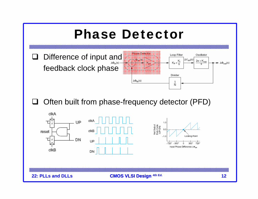
Phase DetectorDifference of input and feedback clock phase
Often built from phase-frequency detector (PFD)
22: PLLs and DLLs 13CMOS VLSI DesignCMOS VLSI Design 4th Ed.
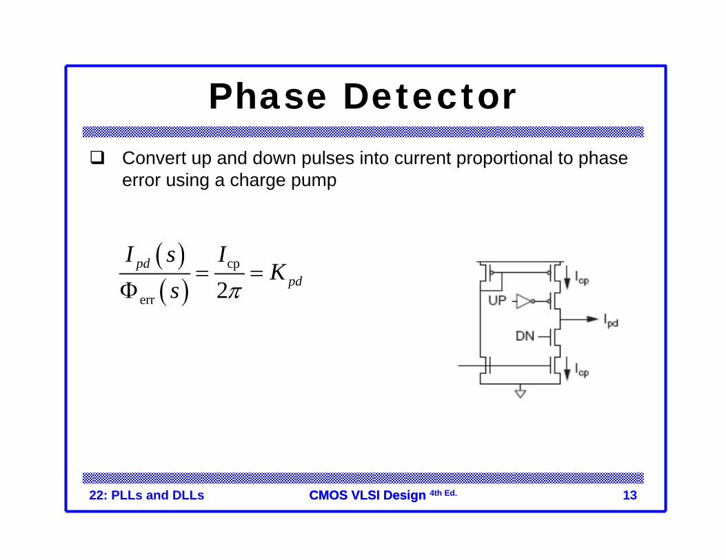
Phase DetectorConvert up and down pulses into current proportional to phase error using a charge pump
( )( )
cp
err 2pd
pd
I s IK
s π= =
Φ
22: PLLs and DLLs 14CMOS VLSI DesignCMOS VLSI Design 4th Ed.
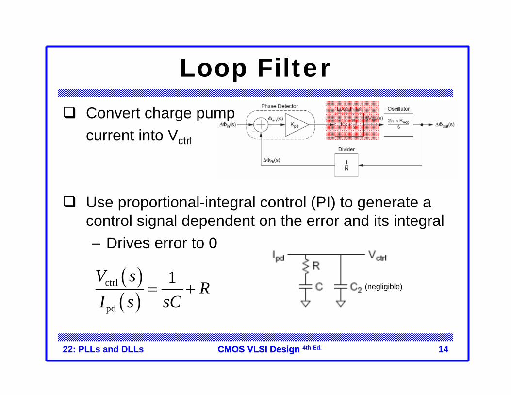
Loop FilterConvert charge pump current into Vctrl
Use proportional-integral control (PI) to generate a control signal dependent on the error and its integral– Drives error to 0
( )( )
ctrl
pd
1V sR
I s sC= + (negligible)

22: PLLs and DLLs 15CMOS VLSI DesignCMOS VLSI Design 4th Ed.
PLL Loop DynamicsClosed loop transfer function of PLL
This is a second order system
ωn indicates loop bandwidthζ indicates damping; choose 0.7 – 1 to avoid ringing
( ) ( )( )
vco
out
vcoin
21
21 11
pd
pd
KK Rs sC sH sKs K R
N sC s
π
π
⎛ ⎞+⎜ ⎟ΔΦ ⎝ ⎠= =ΔΦ ⎛ ⎞+ +⎜ ⎟
⎝ ⎠
( )vco
2
2 2
22
2
cpn
n n
n n n
I Ks NCH s N
s sRC
ωζω ωζω ω ωζ
=+=
+ +=
22: PLLs and DLLs 16CMOS VLSI DesignCMOS VLSI Design 4th Ed.
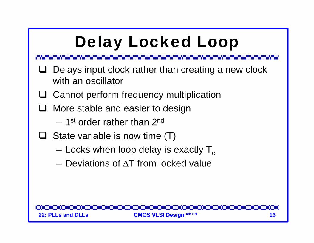
Delay Locked LoopDelays input clock rather than creating a new clock with an oscillatorCannot perform frequency multiplicationMore stable and easier to design– 1st order rather than 2nd
State variable is now time (T)– Locks when loop delay is exactly Tc
– Deviations of ΔT from locked value
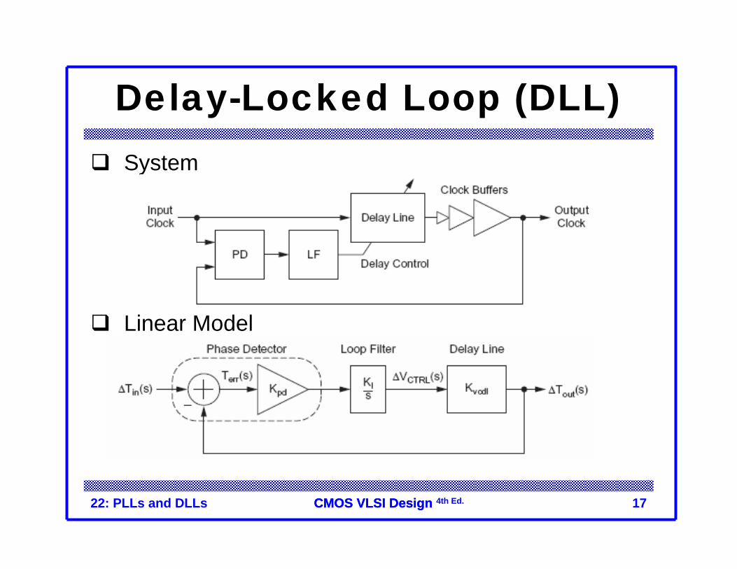
22: PLLs and DLLs 17CMOS VLSI DesignCMOS VLSI Design 4th Ed.
Delay-Locked Loop (DLL)System
Linear Model
22: PLLs and DLLs 18CMOS VLSI DesignCMOS VLSI Design 4th Ed.
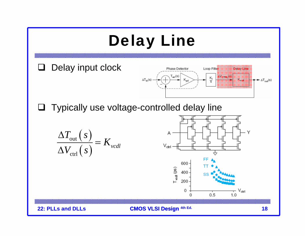
Delay LineDelay input clock
Typically use voltage-controlled delay line
( )( )
out
ctrlvcdl
T sK
V sΔ
=Δ
22: PLLs and DLLs 19CMOS VLSI DesignCMOS VLSI Design 4th Ed.
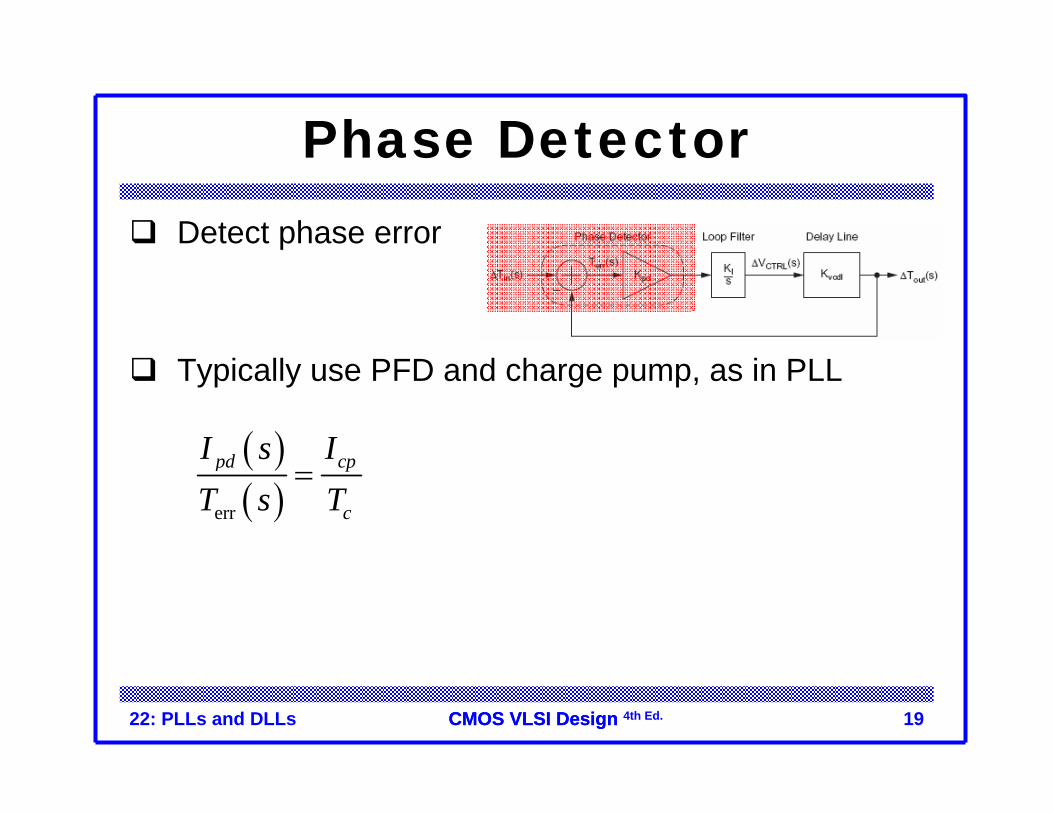
Phase DetectorDetect phase error
Typically use PFD and charge pump, as in PLL
( )( )err
pd cp
c
I s IT s T
=
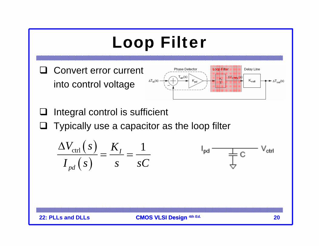
22: PLLs and DLLs 20CMOS VLSI DesignCMOS VLSI Design 4th Ed.
Loop FilterConvert error currentinto control voltage
Integral control is sufficient Typically use a capacitor as the loop filter
( )( )
ctrl 1I
pd
V s KI s s sCΔ
= =

22: PLLs and DLLs 21CMOS VLSI DesignCMOS VLSI Design 4th Ed.
DLL Loop DynamicsClosed loop transfer function of DLL
This is a first order system
τ indicates time constant (inverse of bandwidth)– Choose at least 10Tc for continuous time approx.
( ) ( )( )
out
in
11
T sH s
T s sτΔ
= =Δ +
1 c
pd I vcdl cp vcdl
CTK K K I K
τ = =