Embed Size (px)
Citation preview
http://www.iaeme.com/IJECET/index.asp 91 [email protected]
International Journal of Electronics and Communication Engineering and Technology
(IJECET)
Volume 8, Issue 2, March - April 2017, pp. 91–102, Article ID: IJECET_08_02_013
Available online at
http://www.iaeme.com/IJECET/issues.asp?JType=IJECET&VType=8&IType=2
ISSN Print: 0976-6464 and ISSN Online: 0976-6472
© IAEME Publication
LEAKAGE POWER REDUCTION IN DEEP SUB
MICRON SRAM DESIGN - A REVIEW
Tripti Tripathi
Inderprastha Engineering College, Ghaziabad, Uttar Pradesh, India
Dr. D.S. Chauhan
GLA University, Uttar Pradesh, India
Dr. S. K. Singh
ABES Engineering College, Ghaziabad, Uttar Pradesh, India
ABSTRACT
Present day electronic industry faces the major problem of standby leakage
current, as the processor speed increases, there is requirement of high speed cache
memory. SRAM being mainly used for cache memory design, several low power
techniques are being used for SRAM cell design. Full CMOS 6T SRAM cell is the most
preferred choice for digital circuits. This paper reviews various leakage power
techniques used in 6T SRAM cell and their comparative study.
Key words: CMOS; SRAM; SNM; DRV.
Cite this Article: Tripti Tripathi, Dr. D.S. Chauhan and Dr. S. K. Singh, Leakage
Power Reduction in Deep Sub Micron SRAM Design - A Review, International
Journal of Electronics and Communication Engineering and Technology, 8(2), 2017,
pp. 91–102.
http://www.iaeme.com/IJECET/issues.asp?JType=IJECET&VType=8&IType=2
1. INTRODUCTION
Power consumption particularly off-state leakage current is the major technical problem being
faced by present day electronic industry. As the chip densities increase to a billion of
transistors or more, power is the major limiter of design performance or integration.
According to International Technology Roadmap for Semiconductors (ITRS) projections, the
number of transistors per chip and the local clock frequencies for high- performance
microprocessors will continue to grow exponentially in next 10 years too. As the speed of
microprocessor based electronic equipment increases, there is requirement of large quantity of
data at very high speed which is difficult accomplish. This has led to design of cache memory
as major concern. Mostly SRAM is used for cache memory design and full CMOS 6T SRAM
cell is preferred choice mostly. Static (or leakage) power affects all kinds of Complementary
Metal Oxide Semiconductor (CMOS) circuits but is particularly critical for Static Random
Access Memories (SRAMs) since memories have been designed as performance being the
Tripti Tripathi, Dr. D.S. Chauhan and Dr. S. K. Singh
http://www.iaeme.com/IJECET/index.asp 92 [email protected]
primary figure of merit and also memories are accessed in small portions, thereby leaving vast
majority of memory cells unaccessed for large fraction of time [1]. As reported in
International Technical Roadmap for Semiconductors (ITRS), transistors devoted to memory
structures in microprocessor based system is about 70% today and is expected to increase to
80% in near future [2]. In recent years, the demand for low power has led to development of
different techniques for leakage reduction in SRAM cells at various levels of abstraction;
architecture, device and circuit level. This paper presents exhaustive review of circuit level
techniques to reduce leakage in SRAM cell. There are various architectures of SRAM cell like
6T, 7T, 9T, 12T etc. In this paper 6T CMOS SRAM cell is considered due to its superior
robustness, low power and low voltage operation [3].
2. LEAKAGE COMPONENTS IN BULK CMOS
Leakage power in CMOS transistor originates from various sources corresponding to various
leakage currents flowing in it. Most of the leakage current occurs in standby mode i.e. when
the channel is non- conducting.
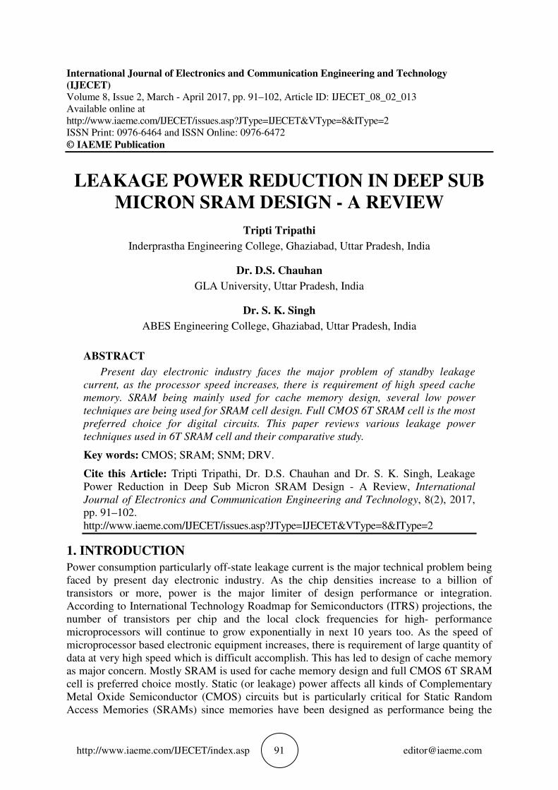
Figure 1 Leakage current components in MOS transistor [4]
Fig.1 shows the main components of leakage current in MOS transistors. Major types of
leakage currents are: sub threshold leakage Isub, gate induced drain leakage IGIDL and depletion
punch through leakage Ipunchthrough. Besides these, gate tunneling leakage through bulk, source
and drain Igb, Igs and Igd (also Igate) and p-n junction leakage current Ijn also exists independent
of the state of channel.
2.2. Subthreshold Leakage Current
It is the drain to source current of a transistor when the gate to source voltage is lower than
threshold voltage (VT). It is due to carrier diffusion between the drain and source regions of
transistor in weak inversion. The behavior of MOS transistor in subthreshold operating region
is similar to that of bipolar device and sub threshold current exhibits exponential dependence
on gate voltage.
2.3. Gate Leakage Current
The electric field across the oxide increases if the thickness of gate oxide is reduced. This
high electric field results in exponential increase of gate oxide tunneling current due to
increase in tunneling probability of electron through the gate oxide.
2.4. Junction Leakage Current
The reverse biased junction leakage current has two main components.
• Caused by EHP generation in the depletion region of reverse biased junction.
• Due to minority carriers diffusion near the edge of depletion region.
Leakage Power Reduction in Deep Sub Micron SRAM Design - A Review
http://www.iaeme.com/IJECET/index.asp 93 [email protected]
The junction leakage current is quite small and mainly exhibits in access transistors of
SRAM memory cell.
In CMOS logic for long channel length (L) transistor, (L> 1µm), very small leakage
current exists. For short channel (L>180nm) and tox>30ºA, subthreshold leakage dominates.
For very small channel length (L>90nm) and tox>20ºA, both subthreshold and gate leakage
are considered and for nanoscaled channel (L< 90nm) and tox< 20ºA, three major leakage
currents considered are: subthreshold leakage, gate leakage and junction leakage current.
Device material technology has managed to keep gate leakage under control by use of high k-
dielectrics. Also the junction leakage current is critical mainly for strong reverse biased
junctions and reverse biasing is used selectively and with moderate amount of bias for
performance reasons, so the major relevant component of leakage current to be considered is
subthreshold leakage.
3. SUBTHRESHOLD LEAKAGE
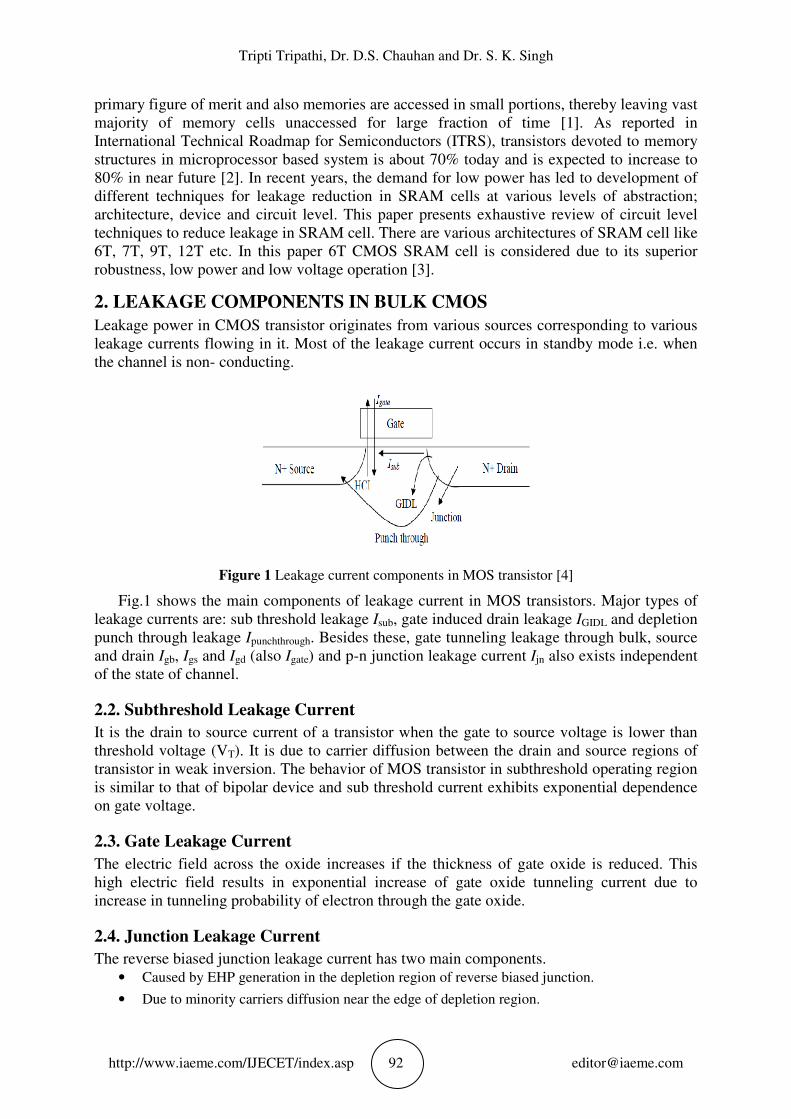
6T SRAM cell depicted in Fig. 2 is used for reference. Subthreshold leakage occurs when
transistor is off and drain to source voltage (Vds) is non-zero. Leakage current can occur either
inside the bit cell or in access transistors paths as shown in Fig. 2.
Figure 2 Leakage Currents in 6T SRAM cell [5]
Which transistor is actually leaking depends on (i) the value stored, (ii) the logic level of
the wordline and (iii) the type of operation (i.e. the value of bitlines).
4. LEAKAGE CURRENT REDUCTION TECHNIQUES
Several different improved design techniques at different level of VLSI design like system,
architectural, circuit and device levels are being put into practice to achieve the objective of
reduced power consumption. These include voltage supply scaling, clock gating, bus
encoding, use of current mode sensing techniques, use of sleep modes, use of data retention
voltage etc. which provide an approach towards reducing energy consumption while
maintaining the performance.
4.1. Device Level Techniques
At this level following techniques are used:
1. New material and process techniques are used to control channel length, oxide thickness,
junction depth and concentration distribution of transistors [6-7].
K. Koh in the year 2003 proposed 6T SRAM cell using buried channel PMOS technology.
The major source of leakage current on NMOS and PMOS devices was different pathways,
and it was controlled by reduction of gate poly-Si oxidation thickness and the optimization of
LDD implantation process.
Tripti Tripathi, Dr. D.S. Chauhan and Dr. S. K. Singh
http://www.iaeme.com/IJECET/index.asp 94 [email protected]
S.Zhao in the year 2004 presented a transistor optimization methodology tailored for
wireless, digital consumer, and mobile applications that employ power management circuit
techniques. This methodology is applied to a 65nm technology that supports a high-density
(<0.5 um2) embedded 6T SRAM cell. High performance logic (Idn/Idp = 550/300uA/um at
Lpoly = 39nm) and low leakage are achieved simultaneously by employing a data retention
mode for the SRAM (Ileakage ∼2pA/bit). Retention mode bias conditions and selective gate
sizing in the SRAM reduces leakage by ∼300X. Advanced transistor design including SSR
channel, strain engineering, drain-extension (HDD) offset spacer, and HDD and halo profile
optimization is used to achieve at least an additional 4× reduction in leakage.
2. An optimized NiSi process, high angle and low dose halo implants contribute to reduced
junction leakage and Gate Induced Drain Leakage [8].
A.Steegan in the year 2005 presented low power SRAM cell using 65nm technology
offering a dual gate oxide process, multiple Vt devices at a nominal operating voltage of
1.2V, a nine level hierarchical Cu interconnect back-end of line process with low k dielectrics
and 0.676mum2 and 0.54mum
2 SRAM cells, optimized for performance and density,
respectively. A gate dielectric with an NFET leakage current as low as 15pA/mum and with
exceptional reliability characteristics has been demonstrated.
3. FINFET are used to improve gate control over the channel length which reduces short
channel effects and subthreshold leakage current [9].
4.2. Architectural Level Techniques
1. This includes multiple mode management which put most unused memory sections into
sleep or turn-off mode to achieve a large leakage reduction because only a small fraction of
SRAM works at a time [10-11].
C.H.Kim in the year 2006 proposed a simple circuit technique that adaptively trades off
overhead energy for maximum leakage savings under severe leakage variations. The proposed
run-time leakage reduction technique for on-die SRAM caches considers architectural access
behavior to determine how often the SRAM blocks should enter a sleep mode. A self-decay
circuit generates a periodic sleep pulse with an adaptive pulse period, which puts the SRAM
array into a sleep mode more frequently at high leakage conditions (fast process, high
temperature) and vice versa.
4.3. Circuit level techniques
4.3.1. Body biasing Method
Subthreshold leakage current is exponentially dependent on threshold voltage which in turn
depends on substrate bias effect or body effect. Body biasing can be used in standby mode to
raise the threshold voltage and hence reduce sub threshold leakage during standby mode in
SRAM cell. It can be of two types: Reverse body biasing or forward body biasing. But, the
effectiveness of the reverse body-biasing scheme decreases with technology scaling, due to
aggravating of the body effect caused by the shorter channel length. In addition, source- bulk,
drain- bulk leakage current, band-to-band tunneling current exponentially increase at the
source-bulk and drain-bulk PN junctions
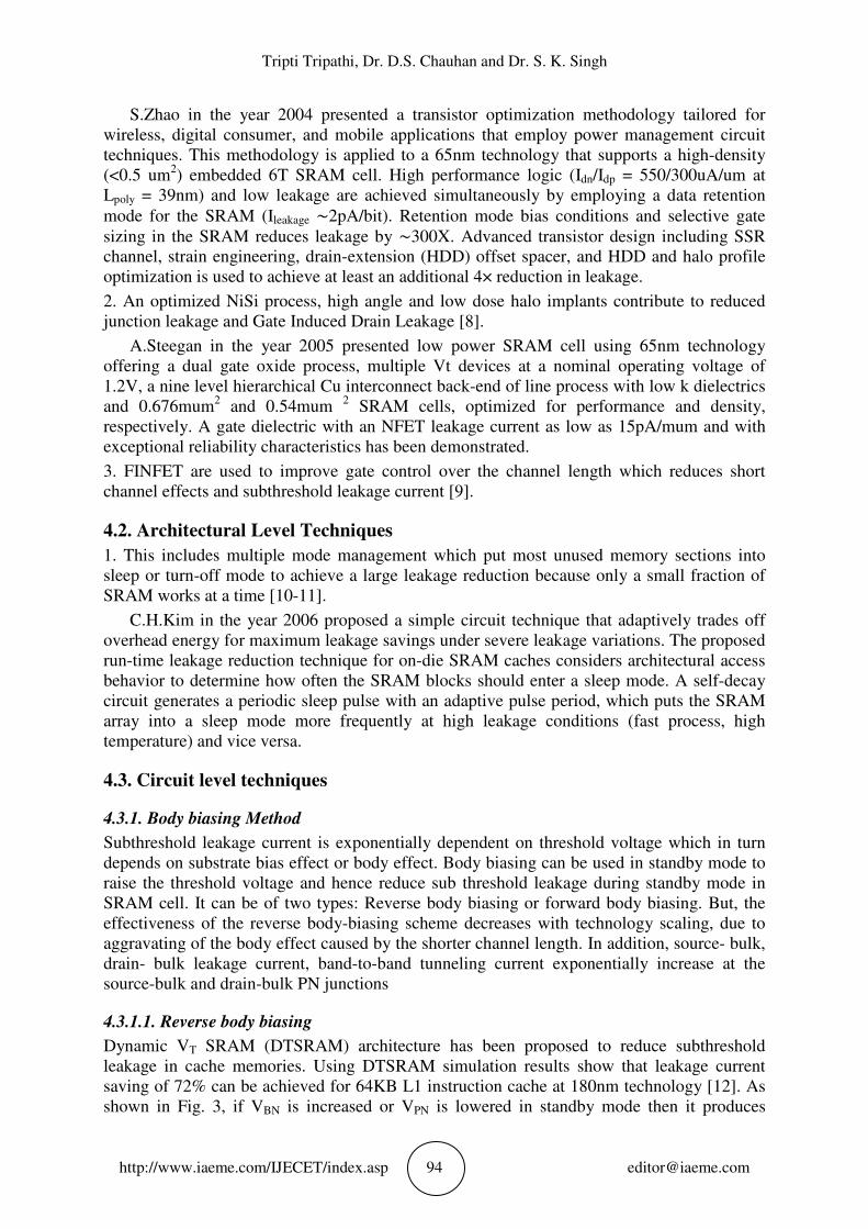
4.3.1.1. Reverse body biasing
Dynamic VT SRAM (DTSRAM) architecture has been proposed to reduce subthreshold
leakage in cache memories. Using DTSRAM simulation results show that leakage current
saving of 72% can be achieved for 64KB L1 instruction cache at 180nm technology [12]. As
shown in Fig. 3, if VBN is increased or VPN is lowered in standby mode then it produces
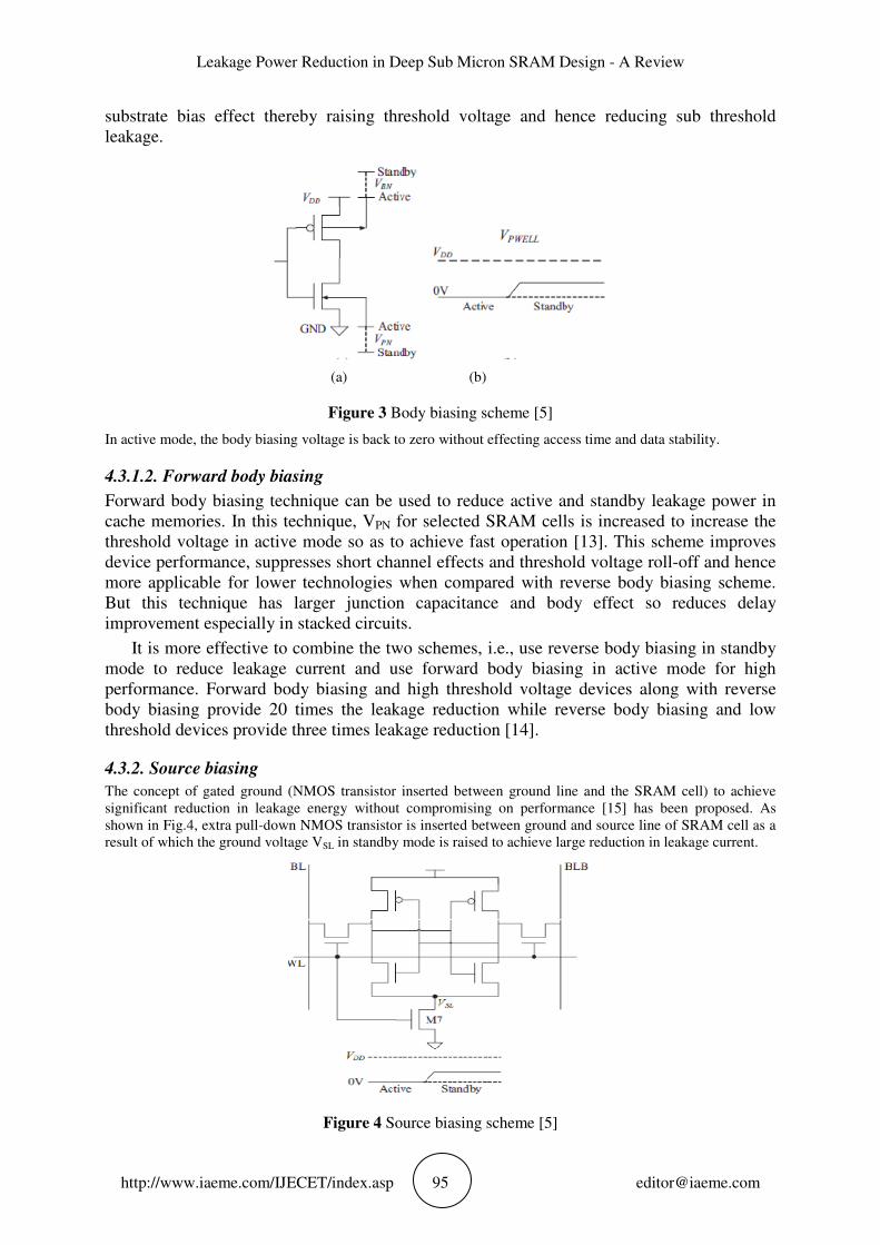
Leakage Power Reduction in Deep Sub Micron SRAM Design - A Review
http://www.iaeme.com/IJECET/index.asp 95 [email protected]
substrate bias effect thereby raising threshold voltage and hence reducing sub threshold
leakage.
(a) (b)
Figure 3 Body biasing scheme [5]
In active mode, the body biasing voltage is back to zero without effecting access time and data stability.
4.3.1.2. Forward body biasing
Forward body biasing technique can be used to reduce active and standby leakage power in
cache memories. In this technique, VPN for selected SRAM cells is increased to increase the
threshold voltage in active mode so as to achieve fast operation [13]. This scheme improves
device performance, suppresses short channel effects and threshold voltage roll-off and hence
more applicable for lower technologies when compared with reverse body biasing scheme.
But this technique has larger junction capacitance and body effect so reduces delay
improvement especially in stacked circuits.
It is more effective to combine the two schemes, i.e., use reverse body biasing in standby
mode to reduce leakage current and use forward body biasing in active mode for high
performance. Forward body biasing and high threshold voltage devices along with reverse
body biasing provide 20 times the leakage reduction while reverse body biasing and low
threshold devices provide three times leakage reduction [14].
4.3.2. Source biasing
The concept of gated ground (NMOS transistor inserted between ground line and the SRAM cell) to achieve
significant reduction in leakage energy without compromising on performance [15] has been proposed. As
shown in Fig.4, extra pull-down NMOS transistor is inserted between ground and source line of SRAM cell as a
result of which the ground voltage VSL in standby mode is raised to achieve large reduction in leakage current.
Figure 4 Source biasing scheme [5]
Tripti Tripathi, Dr. D.S. Chauhan and Dr. S. K. Singh
http://www.iaeme.com/IJECET/index.asp 96 [email protected]
In active mode, WL is high and so M7 is ON, since its resistance is very small so VSL
almost functions as real ground line and SRAM functions as a conventional SRAM cell.
In standby mode, WL is set low so M7 turns off and VSL is high. This results in reduction
of sub-threshold and gate leakage current. High VSL produces body effect that raises threshold
voltage associated with reduced signal rail (VDD-VSL) and so sub-threshold leakage current is
reduced. This scheme also reduces the effect of DIBL due to reduction in voltage difference
between drain and source terminals.
The disadvantage of this scheme is that addition of extra transistor M7 in the pull down
path will get a delay penalty, increasing both area and dynamic energy consumption. To
minimize the area overhead, pull down transistor is often shared by bank of SRAM cells.
4.3.3. Dynamic VDD
In the active mode, a normal supply voltage is applied to a conventional read /write operation,
without delay penalty .Whereas under the standby mode, a reduction in the supply voltage
effectively decreases the sub threshold, gate, and junction leakage current The greatest
drawbacks of this scheme are the substantial increase in the SER (soft error rate), with voltage
scaling, the reduced supply voltage results in a lower static noise margin and possible data
flipping failures and an extra peripheral circuitry such as a high efficiency voltage converter
is required and a significant wake-up access time and dynamic power latency are introduced,
with respect to the conventional 6T SRAM cell, when switching between different modes.
Dual power supply scheme has been proposed to combine with dynamic voltage scheme
[16] to reduce leakage power in SRAM. Subthreshold, gate and junction leakage current can
be effectively reduced by reducing supply voltage in standby mode but it results in lower
SNM and possible data flipping failures. It also requires extra peripheral circuitry such as high
efficiency voltage converter. With lower VDD, leakage power is reduced but it becomes
difficult to guarantee data retention.
It has also been demonstrated that simultaneous use of adaptive body biasing (ABB) and
dynamic voltage scheme (DVS) can be used to reduce power in high-performance processors.
The results demonstrate that application of simultaneous DVS and ABB results in an average
energy reduction of 48% over DVS alone [17].
4.3.4. Negative Wordline
This scheme aims at generating a negative voltage that is supplied to the word line during idle
time without affecting the device performance or SER. Since a negative voltage is supplied,
the access transistors are turned off strongly, thereby leading to a reduction in the sub
threshold leakage current of the access transistors [18]. Row-by-Row dynamic VDD (RDVV)
scheme has been proposed for low power SRAM design where VDD of each row is
dynamically controlled to reduce cell leakage by exploiting DIBL effect [19].
It has also been proposed to use row-by-row dynamic source line voltage control
(RRDSV) technique where the source line shared by neighboring cells is dynamically driven
by voltage higher than VSS to reduce the leakage current when the cells are not activated [20].
The greatest drawbacks of this scheme are that the gate leakage current of access
transistors increases as a result of enlarged gate-source and gate drain voltage differences and
just like the dynamic VDD scheme; there is dynamic power overhead and an extra voltage
generator needed for providing the negative voltage.

Leakage Power Reduction in Deep Sub Micron SRAM Design - A Review
http://www.iaeme.com/IJECET/index.asp 97 [email protected]
Figure 5 Negative wordline scheme [4]
4.3.5. Bitline Floating
Leakage reduction technique by using leakage biased bitlines has been presented for low
power SRAM design [21]. In 6T SRAM cell shown in Fig. 2, when the voltage of bitline
(BLB) is nv1, the voltage difference between source and drain of access transistor M6 is zero,
hence its sub-threshold current is negligible. If memory cells store ‘0’, then BL is set to ‘0’
and BLB is set to ‘1’, this reduces bitline leakage current. The leakage current of access
transistors via DIBL can be reduced in standby mode by the technique that turns-off pre-
charge transistors and allows bitlines to float. The biltlines are disconnected from sense
amplifier by column multiplexer and there is no leakage path introduced.
Figure 6 Bitline Floating scheme [5]
This technique however leads to speed latency due to extra pre-charge cycle.
4.3.6. Multi Threshold CMOS (MTCMOS)
Auto back gate controlled MTCMOS [22] has been presented for low power SRAM design.
The experimental results show that the leakage current is reduced to 1/1000 in sleep mode. It
controls the backgates to reduce the leakage current when the SRAM is not activated (sleep
mode) while retaining the data stored in the memory cells. The active power is 0.27mW/MHz
at 1 V, which is a reduction of 1/12 of a conventional SRAM with a 3.3 V [22]. It uses low VT
transistors to obtain high speed and low leakage while high VT NMOS and PMOS transistors
are placed between the cell and ground and supply and memory cell respectively. In active
mode, high VT transistors are ON and memory cell formed by low VT transistors operates
normally as conventional 6T SRAM cell, while in standby mode high VT transistors are OFF,
transistors go in sleep mode and so the memory cell is disconnected from supply and ground.
This reduces leakage current of memory cell in standby mode.
Tripti Tripathi, Dr. D.S. Chauhan and Dr. S. K. Singh
http://www.iaeme.com/IJECET/index.asp 98 [email protected]
4.3.7. Dual VT and dual tOX Technique
A variation of MTCMOS technique is the Dual VT technique, which uses transistors with two
different threshold voltages. Low-threshold transistors are used for the gates on the critical
path and high-threshold transistors are used for those not in the critical path. Method based on
dual threshold voltage method has been demonstrated to reduce the leakage power dissipation
of SRAMs while maintaining their performance. Experimental results show that this
technique can reduce the leakage-power dissipation of a 64Kb SRAM by more than 35%.
This method improves static noise margin under process variations [23]
In both MTCMOS and Dual VT methods, additional mask layers for each value of
threshold voltage are required for fabricating the transistors selectively according to their
assigned threshold voltage values. This makes the fabrication process complex.
It has also been proposed to use dual VT and dual tOX for low power SRAM design [24],
this method has neither area nor delay overhead. Simulation results with a 65-nm process
demonstrate that this technique can reduce the total leakage power dissipation of a 64 times
512 SRAM array by 33% and that of a 32 times 512 SRAM array by 40%.
4.3.8. PP SRAM Bit cell Structure
PP SRAM Bit –Cell structure has been presented, in which the two NMOS access transistors
(of Fig.2) have been replaced by the two high-VT PMOS access transistors [25]. It is based on
the view that the gate leakage (gate oxide direct tunneling) current will be lower than that of
the leakage offered by the NMOS transistors in the ideal mode of the bit-cell. It utilizes the
Dual Threshold Voltage technology with Forward Body Biasing (FBB) to reduce the
subthreshold leakage without losing the performance. As compared to the conventional 6T
SRAM Bit-cell, this work reduces the total gate leakage current by 27% and the idle power by
37% with no access time degradation and an improvement in the SNM by 15% in 45nm
CMOS technology at VDD = 0.8V.
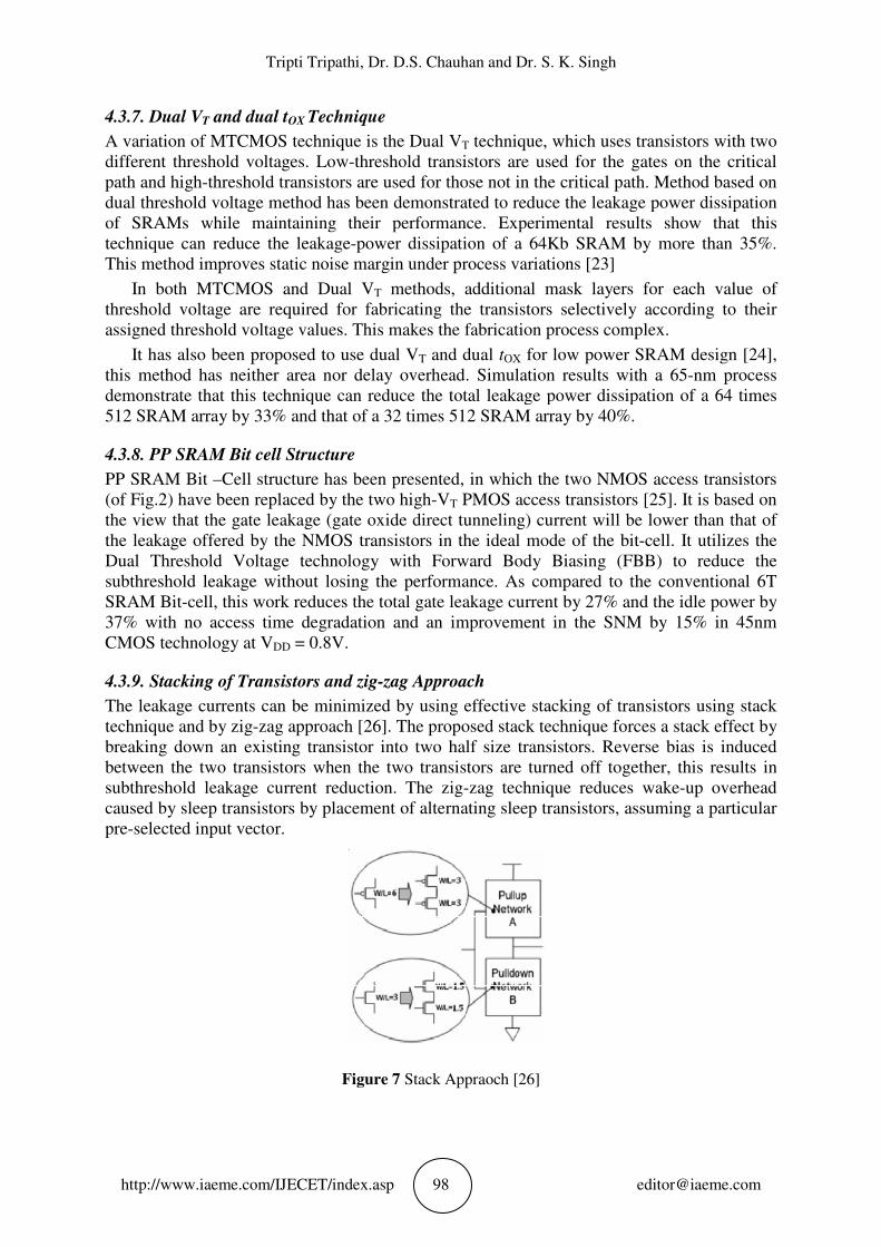
4.3.9. Stacking of Transistors and zig-zag Approach
The leakage currents can be minimized by using effective stacking of transistors using stack
technique and by zig-zag approach [26]. The proposed stack technique forces a stack effect by
breaking down an existing transistor into two half size transistors. Reverse bias is induced
between the two transistors when the two transistors are turned off together, this results in
subthreshold leakage current reduction. The zig-zag technique reduces wake-up overhead
caused by sleep transistors by placement of alternating sleep transistors, assuming a particular
pre-selected input vector.
Figure 7 Stack Appraoch [26]
Leakage Power Reduction in Deep Sub Micron SRAM Design - A Review
http://www.iaeme.com/IJECET/index.asp 99 [email protected]
Simulation results when carried out on 90nm technology demonstrate 35.95% and 91.90%
power saving by zig-zag SRAM and stack SRAM respectively.
4.3.10. Leakage Control Transistor (LECTOR) Technique
LECTOR technique for leakage power reduction in SRAM has been presented [27]. This
approach is based on effective stacking of transistors in the path from supply voltage to
ground. The basic idea behind
LECTOR is based on the concept that a state with more than one transistor OFF in a path
from supply voltage to ground is far less leaky than a state with only one transistor OFF in
any supply to ground path.
5. COMPARISON OF DIFFERENT SRAM LEAKAGE POWER
REDUCTION TECHNIQUES
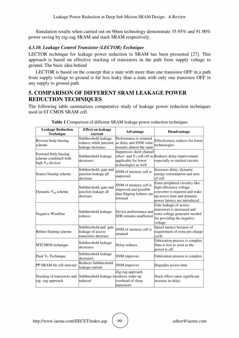
The following table summarizes comparative study of leakage power reduction techniques
used in 6T CMOS SRAM cell.
Table 1 Comparison of different SRAM leakage power reduction techniques
Leakage Reduction
Technique
Effect on leakage
current Advantage Disadvantage
Reverse body biasing
scheme
Subthreshold leakage
reduces while junction
leakage increases
Performance is retained
as delay and SNM value
remains almost the same
Effectiveness reduces for lower
technologies
Forward body biasing
scheme combined with
high Vth devices
Subthreshold leakage
decreases
Suppresses short channel
effect and VT roll-off so
applicable for lower
technologies as well
Reduces delay improvement
especially in stacked circuits
Source biasing scheme
Subthreshold, gate and
junction leakage all
decrease
SNM of memory cell is
improved
Increases delay, dynamic
energy consumption and area
of cell
Dynamic Vdd scheme
Subthreshold, gate and
junction leakage all
decrease
SNM of memory cell is
improved and possible
data flipping failures are
lowered
Extra peripheral circuitry like
high efficiency voltage
converter is required and wake
up access time and dynamic
power latency are introduced.
Negative Wordline Subthreshold leakage
reduces
Device performance and
SER remains unaffected
Gate leakage of access
transistors is increased and
extra voltage generator needed
for providing the negative
voltage
Bitline floating scheme
Subthreshold and gate
leakage of access
transistors decrease
SNM of memory cell is
retained
Speed latency because of
requirement of extra pre-charge
cycle
MTCMOS technique Subthreshold leakage
decreases Delay reduces
Fabrication process is complex.
Data is lost as soon as the
power is off.
Dual VT Technique Subthreshold leakage
decreases SNM improves Fabrication process is complex
PP SRAM bit cell strucure Reduces Subthreshold
leakage current SNM improves Degrades access time
Stacking of transistors and
zig- zag approach
Subthreshold leakage is
reduced
Zig-zag approach
reduces wake-up
overhead of sleep
transistors
Stack effect cause significant
increase in delay.
Tripti Tripathi, Dr. D.S. Chauhan and Dr. S. K. Singh
http://www.iaeme.com/IJECET/index.asp 100 [email protected]
6. CONCLUSION
Standby leakage power in SRAM is of major concern as the technology is scaled down. This
article reviews various existing leakage power reduction techniques and also presents their
comparative study giving advantage and disadvantage of each technique. Each technique has
its own effect on leakage power and device performance and proper trade-off has to be made
between power consumption and device performance.
REFERENCES
[1] Andrea Calimera et al., ‘Design techniques and architectures for low leakage SRAMs’,
IEEE transactions on circuits and systems, vol. 59, No.9, pp. 1992-2007,Sept. 2012.
[2] ‘International technical roadmap for semiconductors’, 2009 available online at http://
www.itrs.net/links/ 2009ITRS/home2009.htm
[3] S. K. Singh et al., ‘Analysis of DRV trade-off in deep submicron SRAM for low power’,
WASJ, pp. 56-62, 2014.
[4] Eitan N. Shauly, “CMOS leakage and power reduction
[5] in transistors and circuits: Process and layout considerations,” Journal of low power
electronics and applications, pp. 1-29, Jan2012
[6] Li-Jun Zhang et al., ‘Leakage power reduction techniques of 55nm SRAM cells’, IETE
Technical Review, Vol. 22, issue 2, pp. 135-145, 2001.
[7] K. Koh et al. ‘Highly manufacturable 100nm 6T low power SRAM with single poly-Si
gate technology’, International Symposium on VLSI Technology, Systems, and
Applications, pp. 64-67, Oct. 2003.
[8] S. Zhao et al., ‘Transistor optimization for leakage power management in a 65nm CMOS
technology for wireless and mobile applications’, International Symposium on VLSI
Technology Digest of Technical Papers. pp. 14-15, Jun. 2004.
[9] A. Steegan et al., ‘65nm CMOS technology for low power applications’, IEEE
International Electron Devices Meeting, Washington DC, pp. 64-67, Dec. 2005.
[10] Z. Guo et al., ‘FINFET based SRAM design’, Proceedings of 2005 International
Symposium on Low Power Electronics and Design, pp. 2-7, Aug. 2005.
[11] C. H. Kim et al., ‘PVT-aware leakage reduction for on-die caches with improved read
stability’, IEEE Journal of Solid-State Circuits, vol. 41, pp. 170-178, Jan. 2006.
[12] K. Flaunter et al., ‘ Drowsy caches: Simple techniques for reducing leakage power’,
Proceedings 29th Annual International Symposium on Computer Architecture,
Anchorage, AK, pp. 148-157, May 2002.
[13] C.H. Kim et al., ‘Dynamic Vt SRAM: A leakage tolerant cache memory for low voltage
microprocessors’, Low Power Electronics and Design, pp. 251-4, 2002.
[14] C.H. Kim et al., ‘A forward body biased low-leakage SRAM cache: device circuit and
architecture considerations’, IEEE Transactions on VLSI Systems, vol. 13, pp. 349-357,
Mar. 2005.
[15] A. Agarwal et al., ‘Leakage power analysis and reduction for nanoscale circuits’, Micro
IEEE, vol. 26, pp. 68-80, 2006.
[16] A. Agarwal et al., ‘A single-Vt low-leakage gated-ground cache for deep submicron’,
IEEE Journal of Solid-State Circuits, vol. 38, pp. 319-328, Feb. 2003.
[17] G. Fukano et al., ‘A 65nm 1Mb SRAM macro with dynamic voltage scaling in dual power
supply scheme for low power SoCs’, International Conference on Memory Technology
and Design, Opio, pp. 18-22, May 2008.
Leakage Power Reduction in Deep Sub Micron SRAM Design - A Review
http://www.iaeme.com/IJECET/index.asp 101 [email protected]
[18] S.M. Martin et al., ‘Combined dynamic voltage scaling and adaptive body biasing for
lower power microprocessors under dynamic workloads’, EE/ACM International
Conference on Computer Aided Design, pp. 721-725, Nov. 2002.
[19] M.D.Singh et al., ‘Leakage power reduction techniques of 45nm static random access
memory (SRAM) cells’, International journal of physical sciences, vol. 6(32), pp.7341-
7353,December 2011.
[20] K. Kanda et al., ‘Two orders of magnitude reduction of low voltage SRAM’s by row by-
row dynamic VDD control (RDDV) scheme,’ Proceedings of IEEE International
ASIC/SOC Conference, NY, USA, pp. 381-385, Sep. 2002.
[21] K.S. Min et al., ‘Row-by-Row dynamic source line voltage control (RRDSV) scheme for
two orders of magnitude leakage current reduction of sub 1V VDD SRAM’s’, IEICE Trans.
Electron, vol. E88-C, No. 4, pp. 760-767, April 2005.
[22] S. Heo et al., ‘Dynamic fine-grain leakage reduction using leakage-biased bitlines’,
Proceedings of the 29th Annual International Symposium on Computer Architecture,
Anchorage, AK, USA, pp. 137-147, 2002.
[23] K. Nii et al., ‘A low power SRAM using auto-backgate-controlled MT-CMOS’,
International symposium on low power electronics and design, USA, pp. 293-298, Aug.
1998.
[24] B. Amelifrad et al., ‘Low leakage SRAM design with dual VT transistors’, Proceedings of
the 7th International Symposium on Quality Electronic Design, pp.729-734, 2006
[25] B. Amelifard et al., ‘Leakage minimization of SRAM cells in a dual-Vt and dual-Tox
technology’, IEEE Transactions on Very Large Scale Integration (VLSI) Systems, vol.16,
pp. 851-859, July 2008.
[26] G. Razavipour et al., ‘Design and Analysis of Two Low-Power SRAM Cell Structures’,
IEEE Transaction on Very Large Scale Integration (VLSI) Systems, Vol. 17, No. 10, pp.
1551-1555, Oct. 2009.
[27] S. P. Vanigalla et al., ‘To reduce SRAM subthreshold leakage using stack and zig-zag
techniques’, International Journal of Scientific Engineering and Technology, vol1, issue
no.2, pp. 51-54, April 2012.
[28] S. Rathore, ‘Low Leakage Power SRAM Design Using Lector Technique in Various
CMOS Technology’, International Journal of Advanced Research in Computer Science
and Software Engineering, vol.4, issue 6, pp.279-284, June 2014.
[29] S. Shigematsu et al., ‘A 1-V High-Speed MTCMOS Circuit Scheme for Power-Down
Application Circuits’, IEEE Journal of Solid-State Circuits, Vol. 32, No. 6, June 1997
[30] N. K. Shukla et al., ‘A Novel Approach to Reduce the Gate and Sub-threshold Leakage in
a Conventional SRAM Bit-Cell Structure at Deep-Sub Micron CMOS Technology’,
International Journal of Computer Applications (IJCA), Vol. 23, No. 7, pp. 23-28, 2011.
[31] N. K. Shukla et al., ‘Speed and Leakage Power Trade-off in Various SRAM Circuits’,
International Journal of Computer and Electrical Engineering (IJCEE), Singapore, Vol.3,
No.2, pp. 244-249, Apr. 2011.
[32] K. Roy and S. C. Prasad, Low-Power CMOS VLSI Circuit Design. New York: Wiley,
2000, ch.5, pp. 214–219.
[33] N. Azizi et al., ‘An asymmetric SRAM cell to lower gate leakage’, proceedings of
International Symposium on Quality Electronic Design, pp.534-539, March 2004
[34] T. Song et. al., “14nm FinFET 128 Mb SRAM with Vmin Enhancement Techniques for
Low-Power Applications,” IEEE Journal Of Solid-State Circuits, Vol. 50, No. 1, Pp 158-
169, January 2015.
Tripti Tripathi, Dr. D.S. Chauhan and Dr. S. K. Singh
http://www.iaeme.com/IJECET/index.asp 102 [email protected]
[35] H. Jeong et. al., “Offset-Compensated Cross-Coupled PFET Bit-Line Conditioning and
Selective Negative Bit-Line Write Assist for High-Density Low-Power SRAM,” IEEE
Transactions On Circuits And Systems—I: Regular Papers, VOL. 62, NO. 4, pp. 1062-
1070,APRIL 2015.
[36] J. Park et. al., “Design of a 22-nm FinFET-Based SRAM With Read Buffer for Near-
Threshold Voltage Operation” IEEE Transactions On Electron Devices, VOL. 62, NO. 6,
pp. 1698-1704, JUNE 2015.
[37] S. Muhammad et. al., “Eight-FinFET Fully Differential SRAM Cell With Enhanced Read
and Write Voltage Margins,” IEEE Transactions on Electron Devices, VOL. 62, NO. 6,
pp-2014-2021,JUNE 2015.
[38] J. S. Shah et. al., “A 32 kb Macro with 8T Soft Error Robust, SRAM Cell in 65-nm
CMOS,” IEEE Transactions on Nuclear Science, VOL. 62, NO. 3, JUNE 2015.
[39] S.K. Singh et. al., “ Deep sub-micron SRAM design for DRV analysis and low leakage,”
International Journal of advances in engineering and technology, vol.1, issue 5, pp- 429-
436, November 2011