Embed Size (px)
Citation preview

CPE 200L DIGITAL LOGIC DESIGN II
DEPARTMENT OF ELECTRICAL AND COMPUTER ENGINEERING 1
CPE 200L DIGITAL LOGIC DESIGN II
LABORATORY 4: INTRODUCTION TO DE2 BOARD
DEPARTMENT OF ELECTRICAL AND COMPUTER ENGINEERING UNIVERSITY OF NEVADA, LAS VEGAS
GOALS:
Getting familiar with DE2 board installation, properties, usage. Programming simple circuit using
Altera Quartus.
BACKGROUND:
Altera’s DE2 Development and Education Board has been developed to provide an ideal
vehicle for learning about digital logic and computer organization in a laboratory setting. It uses the
state-of-the-art technology in both hardware and CAD tools to expose students to a wide range of
topics covered in typical courses. The power of the board is such that it is also highly suitable for a
variety of design projects as well as for the development of sophisticated digital systems. In
addition to the DE2 board and the associated software, Altera provides supporting materials that
include tutorials, laboratory exercises, and interesting demonstrations [1].
The DE2 board features a powerful CycloneR II FPGA chip. All important components on the
board are connected to the pins of this chip, allowing the user to configure the connection between
the various components as desired. For simple experiments, the DE2 board includes a sufficient
number of switches (of both toggle and pushbutton variety), LEDs, and 7-segment displays. For
more advanced experiments, there are SRAM, SDRAM, and Flash memory chips, as well as a
16x2 character display. For experiments that require a processor and simple I/O interfaces, it is
easy to instantiate Altera’s Nios II processor and use interface standards such as RS-232 and PS/2.
For experiments that involve sound or video signals, there are standard connectors provided on the
board. For large design projects, it is possible to use USB and Ethernet connections, as well as the
SD memory card. Finally, it is possible to connect other user-designed boards to the DE2 board by
means of two expansion headers. Continue reading at
http://faculty.unlv.edu/eelabs/docs/guides/DE2_tut_initialDE2.pdf

CPE 200L DIGITAL LOGIC DESIGN II
DEPARTMENT OF ELECTRICAL AND COMPUTER ENGINEERING 2
SETTING UP DE2 BOARD:
The following procedure configures DE2 on the PC computer. Please note, that for TBE-B350 and
TBE-B311 labs, the effects of this procedure will disappear when you log out of lab station
computer. You have to repeat the procedure at the start of each lab if you plan to work with DE2
board.
1. Plug the DC adapter
2. Connect board using USB to the PC computer. Remember to use leftmost connector
3. Click ‘Start’, right-click ‘Computer’ and select ‘Properties’:

CPE 200L DIGITAL LOGIC DESIGN II
DEPARTMENT OF ELECTRICAL AND COMPUTER ENGINEERING 3
Click ‘Device manager’:
You will see the list of devices, look for ‘USB-Blaster’, should be under the section ‘Other
devices’:

CPE 200L DIGITAL LOGIC DESIGN II
DEPARTMENT OF ELECTRICAL AND COMPUTER ENGINEERING 4
Click ‘Update driver’:
Use ‘Browse my computer for driver software:’

CPE 200L DIGITAL LOGIC DESIGN II
DEPARTMENT OF ELECTRICAL AND COMPUTER ENGINEERING 5
Browse to: “C:\altera\71\quartus\drivers\usb-blaster\x64”
After clicking ‘Next’, the following popup can appear:
Answer “Install this driver software anyway”:

CPE 200L DIGITAL LOGIC DESIGN II
DEPARTMENT OF ELECTRICAL AND COMPUTER ENGINEERING 6
If the installation is successful, you should receive:

CPE 200L DIGITAL LOGIC DESIGN II
DEPARTMENT OF ELECTRICAL AND COMPUTER ENGINEERING 7
IMPLEMENTING SIMPLE PROJECT IN QUARTUS
In this section, it is demonstrated how to put very simple circuit to the DE2 board. Inputs will be
connected to switches, output will be connected to LED.
DESIGN AN SIMULATING SCHEMATICS
1. Start Quartus II 7.1 Web Edition
2. Start new project wizard, enter the name of the project of:
Click ‘Next’ twice to go to the screen – Family & Device Settings.
Select the properties that are matching with your DE2 board. Take a look at the FPGA chip on the
board to verify that below properties match with the ones you have:
Family: Cyclone II
Device: EP2C35F672C6

CPE 200L DIGITAL LOGIC DESIGN II
DEPARTMENT OF ELECTRICAL AND COMPUTER ENGINEERING 8
Click Finish.
3. Go to File -> New and select Block Diagram/Schematic File:
4. Add XOR gate to schematics:

CPE 200L DIGITAL LOGIC DESIGN II
DEPARTMENT OF ELECTRICAL AND COMPUTER ENGINEERING 9
5. Use the same panel to add input and output pins, to get the following:
Double click the pin to set its name (a, b – for inputs, y – for output).
6. Add simulation waveform file: go to File –> New, choose Vector Waveform File:

CPE 200L DIGITAL LOGIC DESIGN II
DEPARTMENT OF ELECTRICAL AND COMPUTER ENGINEERING 10
7. Save your files. Go to Assignments -> Settings, choose Simulator Settings section. Set:
Simulation mode: Functional
Simulation input: your saved vector waveform file.
8. Run Processing -> Start Compilation and Simulation. Wait for the message about the end
of the processing (Compile and Simulation was successful).
9. Run Processing -> Start -> Start Analysis & Synthesis.

CPE 200L DIGITAL LOGIC DESIGN II
DEPARTMENT OF ELECTRICAL AND COMPUTER ENGINEERING 11
10. Go to wector waveform view, right click the area on the left and select Insert -> Insert Node
or Bus
Click Node Finder:

CPE 200L DIGITAL LOGIC DESIGN II
DEPARTMENT OF ELECTRICAL AND COMPUTER ENGINEERING 12
Set Filter: Pins: all, click List, then click >> to add three nodes
11. Right clicking on the input waveform allows setting values. Use it to set test values for
simulation, selecting either Forcing High (1) or Forcing Low (0).

CPE 200L DIGITAL LOGIC DESIGN II
DEPARTMENT OF ELECTRICAL AND COMPUTER ENGINEERING 13
You should get:
12. Run Processing -> Generate Functional Simulation Netlist.
13. Start simulation: click Processing -> Start Simulation.
You should get simulation results like below, confirming the operation of XOR gate:
Now you are sure that your schematic works as expected, as the truth table for XOR function is
verified:
a b y Time
0 0 0 0 – 10ns
1 0 1 10ns – 20ns
0 1 1 20ns – 30ns
1 1 0 30ns – 40ns
The next step is to put your design to the board.

CPE 200L DIGITAL LOGIC DESIGN II
DEPARTMENT OF ELECTRICAL AND COMPUTER ENGINEERING 14
PROGRAMMING DE2 BOARD
1. Assign pins. Go to Assignments -> Assignment Editor.
2. Set Category: Pin
3. Double click To field in row number 1.
4. Use the document Altera DE2 Board Pin Table
http://faculty.unlv.edu/eelabs/docs/guides/DE2_Pin_Table.pdf to determine the relation
between pin and physical element on the board. We want to use:
Switch SW0 as first input a
Switch SW1 as second input b
Red LED 0 as the output.
In the Altera DE2 Board Pin Table document, we can see, that switch SW0 is connected to
pin PIN_N25:
Thus we fill the following fields:
Use the Altera DE2 Board Pin Table document to determine the location of two remaining
elements: b, and y. You should get:
Compile your project.

CPE 200L DIGITAL LOGIC DESIGN II
DEPARTMENT OF ELECTRICAL AND COMPUTER ENGINEERING 15
5. Make sure, that SW19 RUN/PROG switch is in the RUN position.
6. Select Tools -> Programmer. Click Hardware Setup and select USB-Blaster from drop-
down list.
Close window.
7. Ensure that Mode value is set to JTAG.
8. If SOF file is not present on the list, click Add file to add it. Make sure Program/Configure
checkbox is checked.
9. Click Start and wait for the board to be programmed. Observe System Messages to see if
programming process ended with success.
CPE 200L DIGITAL LOGIC DESIGN II
DEPARTMENT OF ELECTRICAL AND COMPUTER ENGINEERING 16
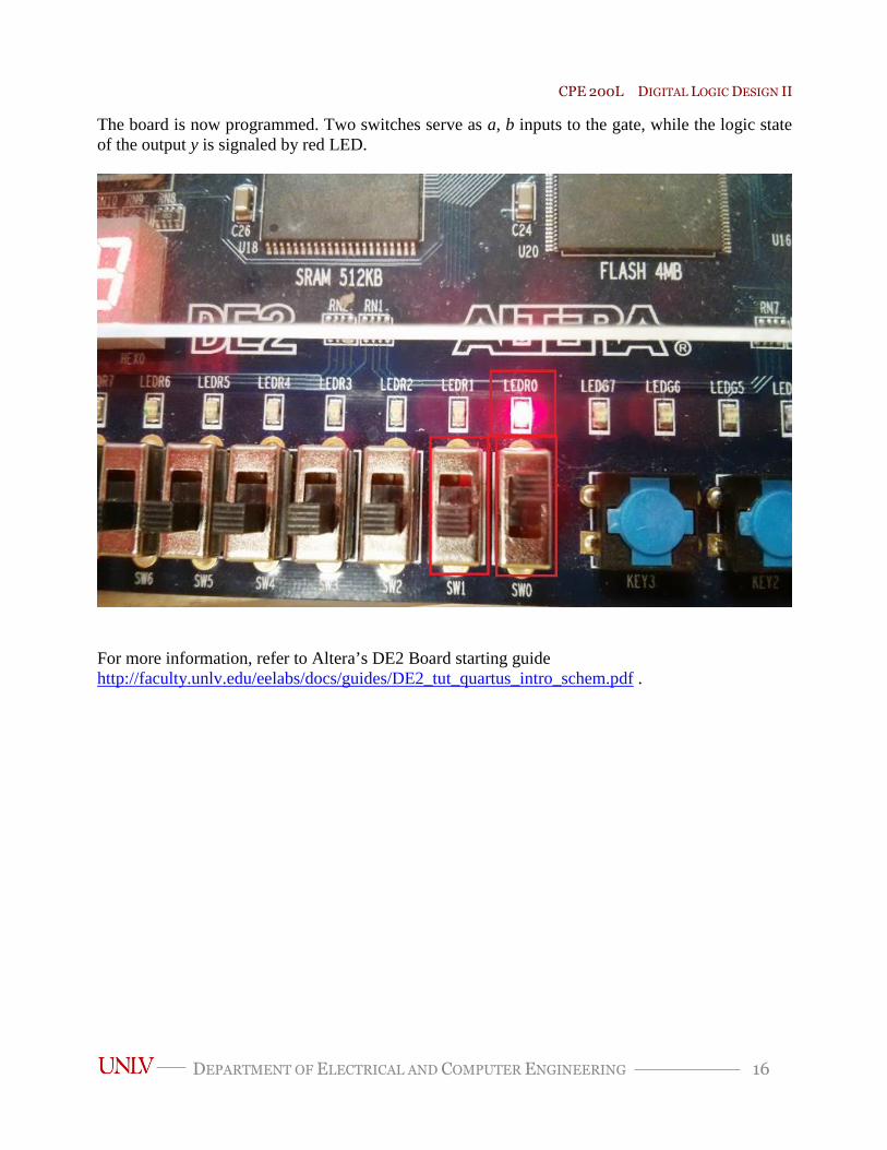
The board is now programmed. Two switches serve as a, b inputs to the gate, while the logic state
of the output y is signaled by red LED.
For more information, refer to Altera’s DE2 Board starting guide
http://faculty.unlv.edu/eelabs/docs/guides/DE2_tut_quartus_intro_schem.pdf .

CPE 200L DIGITAL LOGIC DESIGN II
DEPARTMENT OF ELECTRICAL AND COMPUTER ENGINEERING 17
CREATING A SYMBOL IN QUARTUS
Quartus II software offers the possibility to create user defined elements. This simplifies the
schematic design, as larger parts of the circuit can be represented as a block with inputs and
outputs.
Creating your own Full Adder block:
1. Create Full Adder circuit:
2. Compile your project
3. Create your element: go to File Create / Update Create Symbol Files for Current File. In
the save dialog, put the name of new element, e.g. TestFA.
After the process is done, the element can be selected from the list in Symbol Tool. Go to Windows
Explorer and navigate to the folder that contains your project. You'll see TestFA.bsf file, that was
created. This file contains the definition of your new symbol.

CPE 200L DIGITAL LOGIC DESIGN II
DEPARTMENT OF ELECTRICAL AND COMPUTER ENGINEERING 18
When you type the name you gave to new element – it will appear as any other element:
Now it can be used in the schematic design. Double-clicking the element in the schematic, will
show the inside design of your element.
Using new element in another projects
To use your element in another project, copy the file containing symbol definition (here:
TestFA.bsf) and bdf file to the project directory. Then it will appear in the Symbol Tool.

CPE 200L DIGITAL LOGIC DESIGN II
DEPARTMENT OF ELECTRICAL AND COMPUTER ENGINEERING 19
PROGRAMMING DE2 BOARD WITH VERILOG IN QUARTUS
DE2 offers four 50MHz signals. The frequency of 50MHz can be brought down using the
following procedure. Create a new project named onehertz. Now, instead of creating a new Block
Diagram/Schematic File, choose Verilog HDL File. Copy and paste the onehertz.v code (shown
below). After compilation, the steps are the same as when using a schematic entry.
Map the input “clk_50mhz” to PIN_N2, which is a 50MHz clock internal to the DE2 board. Map
the output “clk_1hz” to LEDG8. On the DE2 board, you should see the LED on for 0.5 seconds
(period of 1 second for both on and off part of the cycle).
module onehertz(clk_50mhz, clk_1hz);
input clk_50mhz;
output clk_1hz;
reg clk_1hz;
reg [24:0] count;
always @ (posedge clk_50mhz)
begin
if(count == 24999999) begin
count <= 0;
$dumpfile("f.vcd");
clk_1hz <= ~clk_1hz;
end
else begin
count <= count + 1;
end
end
endmodule

CPE 200L DIGITAL LOGIC DESIGN II
DEPARTMENT OF ELECTRICAL AND COMPUTER ENGINEERING 20
TROUBLESHOOTING
Quartus schematics:
Compilation errors:
o Make sure schematic does not contain any floating elements
o Make sure that all input and output pins are connected to the elements
No pins showing in node finder:
o Make sure you have performed Compilation
o Make sure you have performed Analysis & Synthesis
Output signal changes with delay to input signals:
o This is probably correct – for Timing simulation. Probably you expect Functional
simulation. Set that in Simulation Options.
New symbol can’t be found in other projects:
o copy the file containing symbol definition (bsf file) and bdf file to the project
directory. Then it will appear in the Symbol Tool.
Programming the board:
Quartus does not see the board:
o Make sure that USB-Blaster is installed
o Make sure that Windows device manager indicates that USB-Blaster device works
properly
o Make sure you connected USB cable to BLASTER port on the board
Board is visible, but there are errors while programming the board:
o Make sure that Family and Device values are set exactly to ones that you can read
from FPGA chip on your board
o Make sure that RUN/PROG switch is in RUN position
LAB DELIVERIES:
PRELAB:
1. Get familiar with Altera DE2 introduction documents
Make yourself familiar with the following documents:
Getting started with Altera DE2 Board:
http://faculty.unlv.edu/eelabs/docs/guides/DE2_tut_initialDE2.pdf
Altera DE2 Introduction
http://faculty.unlv.edu/eelabs/docs/guides/DE2_Introduction_box.pdf
Altera DE2 User Manual
http://faculty.unlv.edu/eelabs/docs/guides/DE2_UserManuall.pdf
Altera: Quartus II Introduction Using Schematic Design
http://faculty.unlv.edu/eelabs/docs/guides/DE2_tut_quartus_intro_schem.pdf
2. Prelab deliveries
Write few paragraphs about FPGA technology

CPE 200L DIGITAL LOGIC DESIGN II
DEPARTMENT OF ELECTRICAL AND COMPUTER ENGINEERING 21
LAB EXPERIMENTS:
1. Experiment 1: Configure DE2 board in Windows system
Use the chapter ‘Setting up DE2 board’ from this lab instruction to setup the DE2 board.
Follow the section Implementing Simple Project In Quartus and implement the XOR gate
on the DE2 board. Demonstrate working XOR to the TA. For more in depth features, and
additional capabilities of Quartus see
http://faculty.unlv.edu/eelabs/docs/guides/DE2_tut_quartus_intro_schem.pdf
2. 4-bit counter
a) Create new project, draw the 4-bit counter given below.
Connect A, B, C, and D to output pins that map to LEDR3, LEDR2, LEDR1, and LEDR0,
respectively. Additionally, also connect A, B, C, and D to inputs of a 7447 decoder (which
can be found in Quartus, see Figure below)
There will be eight output pins for the 7447 decoder. To see how to map these pins to a
seven segment display on the DE2 board see the Altera DE2 pin table
https://faculty.unlv.edu/eelabs/docs/guides/DE2_Pin_Table.pdf or the DE2 User Manual
http://faculty.unlv.edu/eelabs/docs/guides/DE2_UserManuall.pdf (pages 30-31).
Note that the 7447 is only meant to display one digit, i.e. the range 0-9 of the counter.
EXTRA CREDIT: Use two 7-segment displays to display the decimal value of the counter
for the entire 0-15 range using two digits. Use additional logic gates to implement this
feature.

CPE 200L DIGITAL LOGIC DESIGN II
DEPARTMENT OF ELECTRICAL AND COMPUTER ENGINEERING 22
3. Creating symbols
1. Create Full Adder as your own symbol.
2. Use option: “File | Create symbol” to create Full Adder as your own symbol (see section
“Creating a Symbol in Quartus” in the introductory part of this document)
3. Use your symbol to create ripple carry adder:
4. Programming DE2 board with Verilog
1. Implement the frequency divider using Verilog (see the section “Programming DE2 Board
with Verilog in Quartus” in the introductory part of this document.
2. Analyze the Verilog code – answer TA: what type of sequential circuit is implemented in
there?
3. Replace the value of 24,999,999 so that the LED is on for 0.25 seconds (period of 0.5
seconds for both on and off cycle). Use the formula
count = (50MHz * LED_time_on) – 1
4. Reprogram the FPGA with your modification to verify. What is the meaning of this
replaced value? Experiment with some other values and write down the conclusions.

CPE 200L DIGITAL LOGIC DESIGN II
DEPARTMENT OF ELECTRICAL AND COMPUTER ENGINEERING 23
POSTLAB REPORT:
Include the following elements in the report document: Section Element
1 Theory of operation Include a brief description of every element and phenomenon that appears during the experiments.
2 Prelab report
3
Results of the experiments
Experiment Experiment Results
1 a. Screenshot of pin assignments
b. Picture of DE2 during operation
2
a. Screenshot of pin assignments
b. Screenshot of schematic in Quartus
c. Picture of DE2 during operation
3
a. Truth table
b. Screenshot of the FA schematic
c. Screenshot of the Ripple Carry circuit
4 a. screenshot of pin assignments
b. screenshot of your Verilog file with your modified count value
4
Answer the questions
Question no. Question
1 What is pin assignment in DE2?
2 When connecting LEDs in DE2 board, why resistors are not used in
schematic?
3 What is the technical meaning of the value that controls the frequency division
in experiment 4?
5 Conclusions Write down your conclusions, things learned, problems met during the lab and how they were solved, etc.
6 Attachments Zip your projects. Send through WebCampus as zip, or provide link to the zip file to shared location
List of attachments to deliver:
1. Your symbol files for FA
2. Project of Ripple Carry Adder
3. Project of counter
4. Project with Verilog code
References:
1. DE2 pin table: http://faculty.unlv.edu/eelabs/docs/guides/DE2_Pin_Table.pdf
2. Altera DE2 Introduction
http://faculty.unlv.edu/eelabs/docs/guides/DE2_Introduction_box.pdf
3. Getting started with Altera DE2 Board:
http://faculty.unlv.edu/eelabs/docs/guides/DE2_tut_initialDE2.pdf
4. Altera: Quartus II Introduction Using Schematic Design
http://faculty.unlv.edu/eelabs/docs/guides/DE2_tut_quartus_intro_schem.pdf
5. Altera DE2 User Manual
http://faculty.unlv.edu/eelabs/docs/guides/DE2_UserManuall.pdf
6. Datasheets of 7400 series chips:
http://faculty.unlv.edu/eelabs/index.html?navi=main_icdatasheets
7. Using DE2 oscillator: https://faculty.unlv.edu/eelabs/docs/guides/DE2_Oscillator.pdf