Embed Size (px)
Citation preview
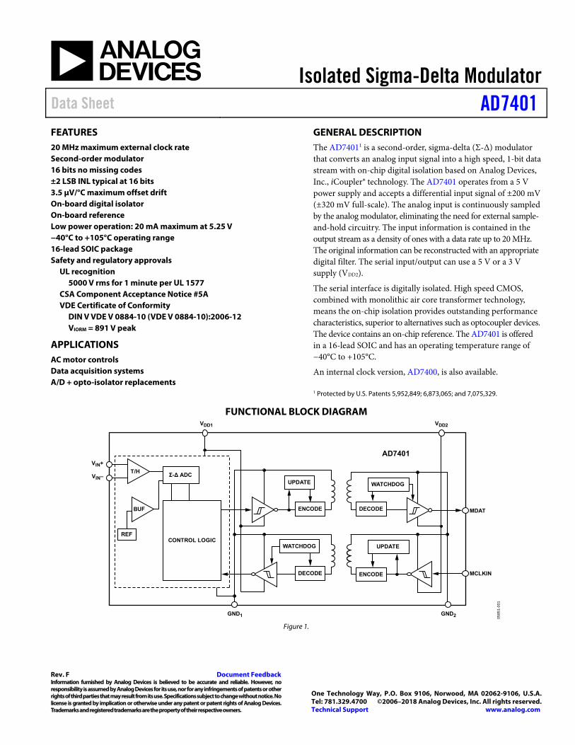
Isolated Sigma-Delta ModulatorData Sheet AD7401
Rev. F Document Feedback Information furnished by Analog Devices is believed to be accurate and reliable. However, no responsibility is assumed by Analog Devices for its use, nor for any infringements of patents or other rights of third parties that may result from its use. Specifications subject to change without notice. No license is granted by implication or otherwise under any patent or patent rights of Analog Devices. Trademarks and registered trademarks are the property of their respective owners.
One Technology Way, P.O. Box 9106, Norwood, MA 02062-9106, U.S.A.Tel: 781.329.4700 ©2006–2018 Analog Devices, Inc. All rights reserved. Technical Support www.analog.com
FEATURES 20 MHz maximum external clock rate Second-order modulator 16 bits no missing codes ±2 LSB INL typical at 16 bits 3.5 μV/°C maximum offset drift On-board digital isolator On-board reference Low power operation: 20 mA maximum at 5.25 V −40°C to +105°C operating range 16-lead SOIC package Safety and regulatory approvals
UL recognition 5000 V rms for 1 minute per UL 1577
CSA Component Acceptance Notice #5A VDE Certificate of Conformity
DIN V VDE V 0884-10 (VDE V 0884-10):2006-12 VIORM = 891 V peak
APPLICATIONS AC motor controls Data acquisition systems A/D + opto-isolator replacements
GENERAL DESCRIPTION The AD74011 is a second-order, sigma-delta (Σ-Δ) modulator that converts an analog input signal into a high speed, 1-bit data stream with on-chip digital isolation based on Analog Devices, Inc., iCoupler® technology. The AD7401 operates from a 5 V power supply and accepts a differential input signal of ±200 mV (±320 mV full-scale). The analog input is continuously sampled by the analog modulator, eliminating the need for external sample-and-hold circuitry. The input information is contained in the output stream as a density of ones with a data rate up to 20 MHz. The original information can be reconstructed with an appropriate digital filter. The serial input/output can use a 5 V or a 3 V supply (VDD2).
The serial interface is digitally isolated. High speed CMOS, combined with monolithic air core transformer technology, means the on-chip isolation provides outstanding performance characteristics, superior to alternatives such as optocoupler devices. The device contains an on-chip reference. The AD7401 is offered in a 16-lead SOIC and has an operating temperature range of −40°C to +105°C.
An internal clock version, AD7400, is also available. 1 Protected by U.S. Patents 5,952,849; 6,873,065; and 7,075,329.
FUNCTIONAL BLOCK DIAGRAM
VIN+
VDD1 VDD2
VIN– Σ-∆ ADC
CONTROL LOGIC
AD7401
BUF
T/H
REF
WATCHDOG
GND1 GND2
MDAT
MCLKINDECODE
ENCODE DECODE
ENCODE
UPDATE
WATCHDOGUPDATE
0585
1-00
1
Figure 1.
AD7401 Data Sheet
Rev. F | Page 2 of 18
TABLE OF CONTENTS Features .............................................................................................. 1 Applications ....................................................................................... 1 General Description ......................................................................... 1 Functional Block Diagram .............................................................. 1 Revision History ............................................................................... 2 Specifications ..................................................................................... 3
Timing Specifications .................................................................. 4 Insulation and Safety Related Specifications ............................ 5 Regulatory Information ............................................................... 5 DIN V VDE V 0884-10 (VDE V 0884-10) Insulation Characteristics .............................................................................. 6
Absolute Maximum Ratings ............................................................ 7 ESD Caution .................................................................................. 7
Pin Configuration and Function Descriptions ............................. 8
Typical Performance Characteristics ..............................................9 Terminology .................................................................................... 12 Theory of Operation ...................................................................... 13
Circuit Information .................................................................... 13 Analog Input ............................................................................... 13 Differential Inputs ...................................................................... 14 Digital Filter ................................................................................ 15
Applications Information .............................................................. 17 Grounding and Layout .............................................................. 17 Evaluating the AD7401 Performance ...................................... 17 Insulation Lifetime ..................................................................... 17
Outline Dimensions ....................................................................... 18 Ordering Guide .......................................................................... 18
REVISION HISTORY 4/2018—Rev. E to Rev. F Changes to Table 3 and Table 4 ....................................................... 5 12/2015—Rev. D to Rev. E Changes to Ordering Guide .......................................................... 18 7/2011—Rev. C to Rev. D Changes to Minimum External Air Gap (Clearance) Parameter, Table 3 and Minimum External Tracking (Creepage) Parameter, Table 3 ................................................................................................ 5 Changes to Figure 5; Pin 1 Description, Table 8; and Pin 7 Description, Table 8 .......................................................................... 8 1/2011—Rev. B to Rev. C Changes to Features Section............................................................ 1 Changes to Input-to-Output Momentary Withstand Voltage Parameter, Table 3, UL Column, Table 4, and Note 1, Table 4 ........ 5 Changes to Ordering Guide ............................................................ 18
9/2007—Rev. A to Rev. B Updated VDE Certification Throughout ...................................... 1 Changes to Table 6 ............................................................................. 7 12/2006—Rev. 0 to Rev. A Changes to Features and General Description .............................. 1 Changes to Table 1 ............................................................................. 3 Changes to Table 2 ............................................................................. 4 Changes to Table 6 ............................................................................. 7 Changes to Table 8 ............................................................................. 8 Changes to Circuit Information Section ..................................... 13 Changes to Figure 27 ...................................................................... 15 1/2006—Revision 0: Initial Version
Data Sheet AD7401
Rev. F | Page 3 of 18
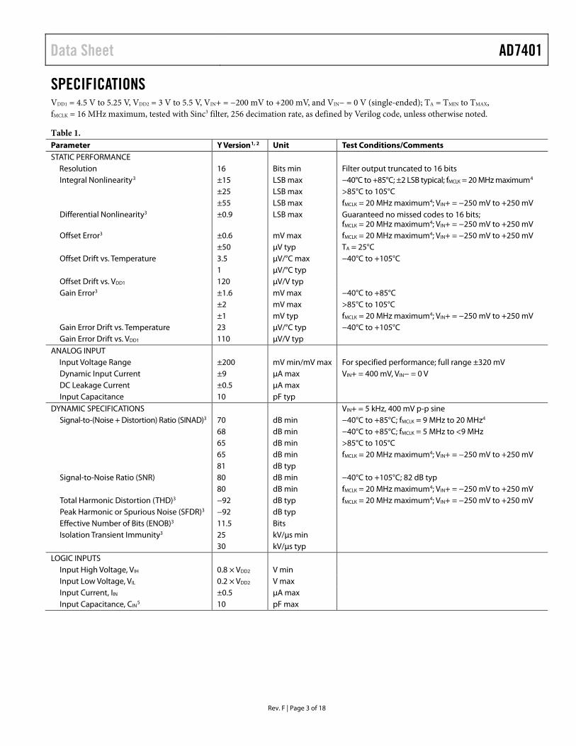
SPECIFICATIONS VDD1 = 4.5 V to 5.25 V, VDD2 = 3 V to 5.5 V, VIN+ = −200 mV to +200 mV, and VIN− = 0 V (single-ended); TA = TMIN to TMAX, fMCLK = 16 MHz maximum, tested with Sinc3 filter, 256 decimation rate, as defined by Verilog code, unless otherwise noted.
Table 1. Parameter Y Version1, 2 Unit Test Conditions/Comments STATIC PERFORMANCE
Resolution 16 Bits min Filter output truncated to 16 bits Integral Nonlinearity3 ±15 LSB max −40°C to +85°C; ±2 LSB typical; fMCLK = 20 MHz maximum4 ±25 LSB max >85°C to 105°C
±55 LSB max fMCLK = 20 MHz maximum4; VIN+ = −250 mV to +250 mV Differential Nonlinearity3 ±0.9 LSB max Guaranteed no missed codes to 16 bits;
fMCLK = 20 MHz maximum4; VIN+ = −250 mV to +250 mV Offset Error3 ±0.6 mV max fMCLK = 20 MHz maximum4; VIN+ = −250 mV to +250 mV ±50 µV typ TA = 25°C Offset Drift vs. Temperature 3.5 µV/°C max −40°C to +105°C 1 µV/°C typ Offset Drift vs. VDD1
120 µV/V typ Gain Error3 ±1.6 mV max −40°C to +85°C ±2 mV max >85°C to 105°C ±1 mV typ fMCLK = 20 MHz maximum4; VIN+ = −250 mV to +250 mV Gain Error Drift vs. Temperature 23 µV/°C typ −40°C to +105°C Gain Error Drift vs. VDD1 110 µV/V typ
ANALOG INPUT Input Voltage Range ±200 mV min/mV max For specified performance; full range ±320 mV Dynamic Input Current ±9 µA max VIN+ = 400 mV, VIN− = 0 V DC Leakage Current ±0.5 µA max Input Capacitance 10 pF typ
DYNAMIC SPECIFICATIONS VIN+ = 5 kHz, 400 mV p-p sine Signal-to-(Noise + Distortion) Ratio (SINAD)3 70 dB min −40°C to +85°C; fMCLK = 9 MHz to 20 MHz4 68 dB min −40°C to +85°C; fMCLK = 5 MHz to <9 MHz 65 dB min >85°C to 105°C 65 dB min fMCLK = 20 MHz maximum4; VIN+ = −250 mV to +250 mV 81 dB typ Signal-to-Noise Ratio (SNR) 80 dB min −40°C to +105°C; 82 dB typ
80 dB min fMCLK = 20 MHz maximum4; VIN+ = −250 mV to +250 mV Total Harmonic Distortion (THD)3 −92 dB typ fMCLK = 20 MHz maximum4; VIN+ = −250 mV to +250 mV Peak Harmonic or Spurious Noise (SFDR)3 −92 dB typ Effective Number of Bits (ENOB)3 11.5 Bits Isolation Transient Immunity3 25 kV/µs min 30 kV/µs typ
LOGIC INPUTS Input High Voltage, VIH 0.8 × VDD2 V min Input Low Voltage, VIL 0.2 × VDD2 V max Input Current, IIN ±0.5 µA max Input Capacitance, CIN
5 10 pF max
AD7401 Data Sheet
Rev. F | Page 4 of 18
Parameter Y Version1, 2 Unit Test Conditions/Comments LOGIC OUTPUTS
Output High Voltage, VOH VDD2 − 0.1 V min IO = −200 μA Output Low Voltage, VOL 0.4 V max IO = +200 μA
POWER REQUIREMENTS VDD1 4.5/5.25 V min/V max VDD2 3/5.5 V min/V max IDD1
6 12 mA max VDD1 = 5.25 V IDD2
7 8 mA max VDD2 = 5.5 V 4 mA max VDD2 = 3.3 V
1 Temperature range is −40°C to +85°C. 2 All voltages are relative to their respective ground. 3 See the Terminology section. 4 For fMCLK > 16 MHz to 20 MHz, mark space ratio is 48/52 to 52/48, VDD1 = VDD2 = 5 V ± 5%, and TA = −40°C to +85°C. 5 Sample tested during initial release to ensure compliance. 6 See Figure 15. 7 See Figure 17.
TIMING SPECIFICATIONS VDD1 = 4.5 V to 5.25 V, VDD2 = 3 V to 5.5 V, TA = TMAX to TMIN, unless otherwise noted.1
Table 2. Parameter Limit at TMIN, TMAX Unit Description fMCLKIN
2, 3 20 MHz max Master clock input frequency 5 MHz min Master clock input frequency t1
4 25 ns max Data access time after MCLK rising edge t2
4 15 ns min Data hold time after MCLK rising edge t3 0.4 × tMCLKIN ns min Master clock low time t4 0.4 × tMCLKIN ns min Master clock high time 1 Sample tested during initial release to ensure compliance 2 Mark space ratio for clock input is 40/60 to 60/40 for fMCLKIN to 16 MHz and 48/52 to 52/48 for fMCLKIN > 16 MHz to 20 MHz. 3 VDD1 = VDD2 = 5 V ± 5% for fMCLKIN > 16 MHz to 20 MHz. 4 Measured with the load circuit of Figure 2 and defined as the time required for the output to cross 0.8 V or 2.0 V.
200µA IOL
200µA IOH
1.6VTO OUTPUTPIN
CL25pF
0585
1-00
2
Figure 2. Load Circuit for Digital Output Timing Specifications
MCLKIN
MDAT
t1 t2
t4
t3
0585
1-00
3
Figure 3. Data Timing

Data Sheet AD7401
Rev. F | Page 5 of 18
INSULATION AND SAFETY RELATED SPECIFICATIONS
Table 3. Parameter Symbol Value Unit Conditions Input-to-Output Momentary Withstand Voltage VISO 5000 min V rms 1-minute duration Minimum External Air Gap (Clearance) L(I01) 7.81,2 min mm Measured from input terminals to output
terminals, shortest distance through air Minimum External Tracking (Creepage) L(I02) 7.81,2 min mm Measured from input terminals to output
terminals, shortest distance path along body Minimum Internal Gap (Internal Clearance) 0.017 min mm Insulation distance through insulation Tracking Resistance (Comparative Tracking Index) CTI >400 V DIN IEC 112/VDE 0303 Part 1 Isolation Group II Material Group (DIN VDE 0110, 1/89, Table I) 1 In accordance with IEC 60950-1 guidelines for the measurement of creepage and clearance distances for a pollution degree of 2 and altitudes ≤2000 m. 2 Consideration must be given to pad layout to ensure the minimum required distance for clearance is maintained.
REGULATORY INFORMATION
Table 4. UL1 CSA VDE2 Recognized under 1577 Component Recognition Program1
Approved under CSA Component Acceptance Notice #5A
Certified according to DIN V VDE V 0884-10 (VDE V 0884-10):2006-122
5000 V rms Isolation Voltage Basic insulation per CSA 60950-1-07 and IEC 60950-1, 780 V rms maximum working voltage. Reinforced insulation per CSA 60950-1-03 and IEC 60950-1, 390 V rms maximum working voltage.
Reinforced insulation per DIN V VDE V 0884-10 (VDE V 0884-10):2006-12, 891V peak
File E214100 File 205078 File 2471900-4880-0001 1 In accordance with UL 1577, each AD7401 is proof tested by applying an insulation test voltage ≥6000 V rms for 1 second (current leakage detection limit = 15 µA). 2 In accordance with DIN V VDE V 0884-10, each AD7401 is proof tested by applying an insulation test voltage ≥1671 V peak for 1 second (partial discharge detection
limit = 5 pC).
AD7401 Data Sheet
Rev. F | Page 6 of 18
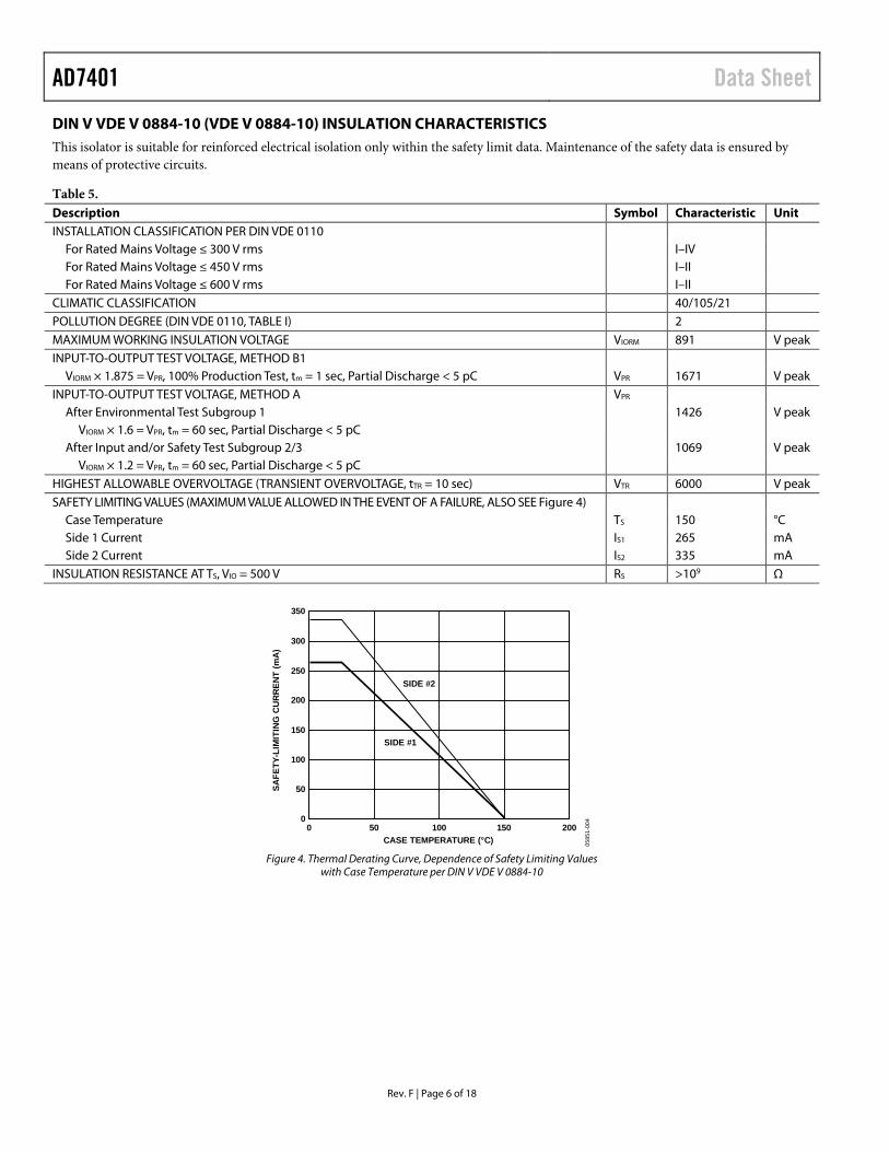
DIN V VDE V 0884-10 (VDE V 0884-10) INSULATION CHARACTERISTICS This isolator is suitable for reinforced electrical isolation only within the safety limit data. Maintenance of the safety data is ensured by means of protective circuits.
Table 5. Description Symbol Characteristic Unit INSTALLATION CLASSIFICATION PER DIN VDE 0110
For Rated Mains Voltage ≤ 300 V rms I–IV For Rated Mains Voltage ≤ 450 V rms I–II For Rated Mains Voltage ≤ 600 V rms I–II
CLIMATIC CLASSIFICATION 40/105/21 POLLUTION DEGREE (DIN VDE 0110, TABLE I) 2 MAXIMUM WORKING INSULATION VOLTAGE VIORM 891 V peak INPUT-TO-OUTPUT TEST VOLTAGE, METHOD B1
VIORM × 1.875 = VPR, 100% Production Test, tm = 1 sec, Partial Discharge < 5 pC VPR 1671 V peak INPUT-TO-OUTPUT TEST VOLTAGE, METHOD A VPR
After Environmental Test Subgroup 1 1426 V peak VIORM × 1.6 = VPR, tm = 60 sec, Partial Discharge < 5 pC
After Input and/or Safety Test Subgroup 2/3 1069 V peak VIORM × 1.2 = VPR, tm = 60 sec, Partial Discharge < 5 pC
HIGHEST ALLOWABLE OVERVOLTAGE (TRANSIENT OVERVOLTAGE, tTR = 10 sec) VTR 6000 V peak SAFETY LIMITING VALUES (MAXIMUM VALUE ALLOWED IN THE EVENT OF A FAILURE, ALSO SEE Figure 4)
Case Temperature TS 150 °C Side 1 Current IS1 265 mA Side 2 Current IS2 335 mA
INSULATION RESISTANCE AT TS, VIO = 500 V RS >109 Ω
CASE TEMPERATURE (°C)
SAFE
TY-L
IMIT
ING
CU
RR
ENT
(mA
)
00
350
300
250
200
150
100
50
50 100 150 200
SIDE #1
SIDE #2
0585
1-00
4
Figure 4. Thermal Derating Curve, Dependence of Safety Limiting Values
with Case Temperature per DIN V VDE V 0884-10
Data Sheet AD7401
Rev. F | Page 7 of 18
ABSOLUTE MAXIMUM RATINGS TA = 25°C, unless otherwise noted. All voltages are relative to their respective ground.
Table 6. Parameter Rating VDD1 to GND1 −0.3 V to +6.5 V VDD2 to GND2 −0.3 V to +6.5 V Analog Input Voltage to GND1 −0.3 V to VDD1 + 0.3 V Digital Input Voltage to GND2 −0.3 V to VDD1 + 0.5 V Output Voltage to GND2 −0.3 V to VDD2 + 0.3 V Input Current to Any Pin Except Supplies1 ±10 mA Operating Temperature Range −40°C to +105°C Storage Temperature Range −65°C to +150°C Junction Temperature 150°C SOIC Package
θJA Thermal Impedance 89.2°C/W θJC Thermal Impedance 55.6°C/W
Resistance (Input to Output), RI-O 1012 Ω Capacitance (Input to Output), CI-O
2 1.7 pF typ Lead-Free Temperature, Soldering
Reflow 260 (+0)°C ESD 1.5 kV 1 Transient currents of up to 100 mA do not cause SCR to latch-up. 2 f = 1 MHz.
Stresses at or above those listed under Absolute Maximum Ratings may cause permanent damage to the product. This is a stress rating only; functional operation of the product at these or any other conditions above those indicated in the operational section of this specification is not implied. Operation beyond the maximum operating conditions for extended periods may affect product reliability.
Table 7. Maximum Continuous Working Voltage1 Parameter Max Unit Constraint AC Voltage, Bipolar Waveform
565 VPK 50-year minimum lifetime
AC Voltage, Unipolar Waveform
891 VPK Maximum CSA/VDE approved working voltage
DC Voltage 891 V Maximum CSA/VDE approved working voltage
1 Refers to continuous voltage magnitude imposed across the isolation barrier. See the Insulation Lifetime section for more details.
ESD CAUTION
AD7401 Data Sheet
Rev. F | Page 8 of 18
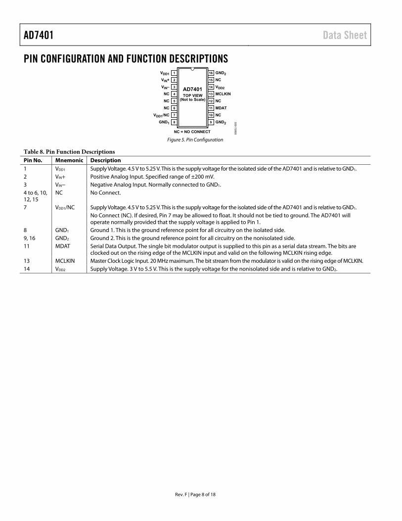
PIN CONFIGURATION AND FUNCTION DESCRIPTIONS VDD1 1
VIN+ 2
VIN– 3
NC 4
GND216
NC15
VDD214
MCLKIN13
NC 5 NC12
NC 6 MDAT11
VDD1/NC 7 NC10
GND1 8 GND29
NC = NO CONNECT
AD7401TOP VIEW
(Not to Scale)
0585
1-00
5
Figure 5. Pin Configuration
Table 8. Pin Function Descriptions Pin No. Mnemonic Description 1 VDD1 Supply Voltage. 4.5 V to 5.25 V. This is the supply voltage for the isolated side of the AD7401 and is relative to GND1. 2 VIN+ Positive Analog Input. Specified range of ±200 mV. 3 VIN− Negative Analog Input. Normally connected to GND1. 4 to 6, 10, 12, 15
NC No Connect.
7 VDD1/NC Supply Voltage. 4.5 V to 5.25 V. This is the supply voltage for the isolated side of the AD7401 and is relative to GND1. No Connect (NC). If desired, Pin 7 may be allowed to float. It should not be tied to ground. The AD7401 will
operate normally provided that the supply voltage is applied to Pin 1. 8 GND1 Ground 1. This is the ground reference point for all circuitry on the isolated side. 9, 16 GND2 Ground 2. This is the ground reference point for all circuitry on the nonisolated side. 11 MDAT Serial Data Output. The single bit modulator output is supplied to this pin as a serial data stream. The bits are
clocked out on the rising edge of the MCLKIN input and valid on the following MCLKIN rising edge. 13 MCLKIN Master Clock Logic Input. 20 MHz maximum. The bit stream from the modulator is valid on the rising edge of MCLKIN. 14 VDD2 Supply Voltage. 3 V to 5.5 V. This is the supply voltage for the nonisolated side and is relative to GND2.
Data Sheet AD7401
Rev. F | Page 9 of 18
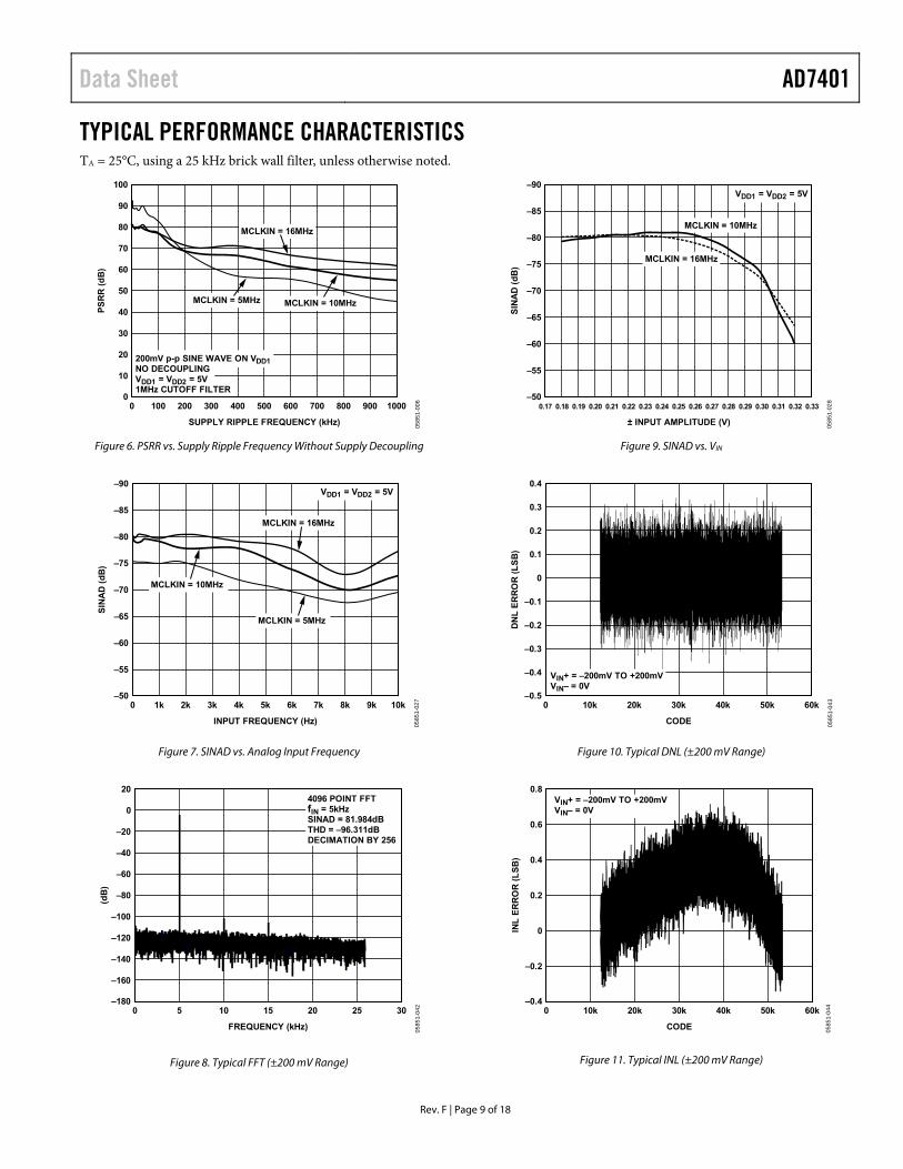
TYPICAL PERFORMANCE CHARACTERISTICS TA = 25°C, using a 25 kHz brick wall filter, unless otherwise noted.
100
00 1000
SUPPLY RIPPLE FREQUENCY (kHz)
PS
RR
(d
B)
90
80
70
60
50
40
30
20
10
100 200 300 400 500 600 700 800 900
MCLKIN = 10MHzMCLKIN = 5MHz
MCLKIN = 16MHz
200mV p-p SINE WAVE ON VDD1NO DECOUPLINGVDD1 = VDD2 = 5V1MHz CUTOFF FILTER
0585
1-00
6
Figure 6. PSRR vs. Supply Ripple Frequency Without Supply Decoupling
–90
–500 10k
INPUT FREQUENCY (Hz)
SIN
AD
(d
B)
–85
–80
–75
–70
–65
–60
–55
1k 2k 3k 4k 5k 6k 7k 8k 9k
VDD1 = V DD2 = 5 VVDD1 = VDD2 = 5V
MCLKIN = 16MHz
MCLKIN = 5MHz
MCLKIN = 10MHz
0585
1-02
7
Figure 7. SINAD vs. Analog Input Frequency
20
–1800 30
FREQUENCY (kHz)
(dB
)
0
–20
–40
–60
–80
–100
–120
–140
–160
5 10 15 20 25
4096 POINT FFTfIN = 5kHzSINAD = 81.984dBTHD = –96.311dBDECIMATION BY 256
0585
1-04
2
Figure 8. Typical FFT (±200 mV Range)
–90
–500.17 0.33
± INPUT AMPLITUDE (V)
SIN
AD
(d
B)
–85
–80
–75
–70
–65
–60
–55
0.18 0.19 0.20 0.21 0.22 0.23 0.24 0.25 0.26 0.27 0.28 0.29 0.30 0.31 0.32
MCLKIN = 16MHz
MCLKIN = 10MHz
VDD1 = VDD2 = 5V
0585
1-02
8
Figure 9. SINAD vs. VIN
0.4
–0.50 60k
CODE
DN
L E
RR
OR
(L
SB
)0.3
0.2
0.1
0
–0.1
–0.2
–0.3
–0.4
10k 20k 30k 40k 50k
VIN+ = –200mV TO +200mVVIN– = 0V
0585
1-04
3
Figure 10. Typical DNL (±200 mV Range)
0.8
–0.40 60k
CODE
INL
ER
RO
R (
LS
B)
0585
1-04
40.6
0.4
0.2
0
–0.2
10k 20k 30k 40k 50k
VIN+ = –200mV TO +200mVVIN– = 0V
Figure 11. Typical INL (±200 mV Range)
AD7401 Data Sheet
Rev. F | Page 10 of 18
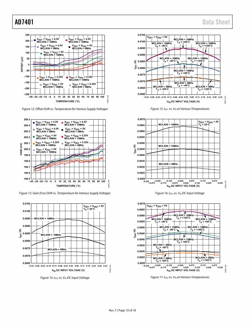
250
–250–45
TEMPERATURE (°C)
OF
FS
ET
(µ
V)
–35 –25 –15 –5 5 15 25 35 45 55 65 75 85 95 105
200
150
100
50
0
–50
–100
–150
–200
VDD1 = VDD2 = 5VMCLKIN = 16MHz
VDD1 = VDD2 = 4.5VMCLKIN = 5MHz
VDD1 = VDD2 = 4.5VMCLKIN = 16MHz
VDD1 = VDD2 = 4.5VMCLKIN = 10MHz
VDD1 = VDD2 = 5VMCLKIN = 5MHz
VDD1 = VDD2 = 5.25VMCLKIN = 16MHz
VDD1 = VDD2 = 5.25VMCLKIN = 10MHz
VDD1 = VDD2 = 5VMCLKIN = 10MHz
VDD1 = VDD2 = 5.25VMCLKIN = 5MHz
0585
1-02
9
Figure 12. Offset Drift vs. Temperature for Various Supply Voltages
200.5
199.5–45
TEMPERATURE (°C)
GA
IN (
mV
)
–35 –25 –15 –5 5 15 25 35 45 55 65 75 85 95 105
200.4
200.3
200.2
200.1
200.0
199.9
199.8
199.7
199.6
VDD1 = VDD2 = 5VMCLKIN = 16MHz
VDD1 = VDD2 = 4.5VMCLKIN = 5MHz
VDD1 = VDD2 = 4.5VMCLKIN = 16MHz
VDD1 = VDD2 = 5.25VMCLKIN = 16MHz
VDD1 = VDD2 = 5VMCLKIN = 10MHz
VDD1 = VDD2 = 4.5VMCLKIN = 10MHz
VDD1 = VDD2 = 5VMCLKIN = 5MHz
VDD1 = VDD2 = 5.25VMCLKIN = 10MHz
VDD1 = VDD2 = 5.25VMCLKIN = 5MHz
0585
1-03
6
Figure 13. Gain Error Drift vs. Temperature for Various Supply Voltages
VIN DC INPUT VOLTAGE (V)
I DD
1 (
A)
–0.33 0.33–0.28 –0.23 –0.18 –0.13 –0.08 –0.03 0.03 0.08 0.13 0.18 0.23 0.280.0065
0.0070
0.0075
0.0080
0.0085
0.0090
0.0095
0.0100
0.0105VDD1 = VDD2 = 5VTA = 25°C
MCLKIN = 16MHz
MCLKIN = 10MHz
MCLKIN = 5MHz
0585
1-03
3
Figure 14. IDD1 vs. VIN DC Input Voltage
VIN DC INPUT VOLTAGE (V)
I DD
1 (
A)
–0.33 0.33–0.28 –0.23 –0.18 –0.13 –0.08 –0.03 0.03 0.08 0.13 0.18 0.23 0.28
0.0060
0.0065
0.0070
0.0075
0.0080
0.0085
0.0090
0.0095
0.0100
0.0105
MCLKIN = 16MHzTA = +85°C MCLKIN = 16MHz
TA = +105°CMCLKIN = 16MHz
TA = –40°C
MCLKIN = 10MHzTA = –40°C
MCLKIN = 10MHzTA = +105°C
MCLKIN = 10MHzTA = +85°C
MCLKIN = 5MHzTA = +105°C
MCLKIN = 5MHzTA = +85°C
MCLKIN = 5MHzTA = –40°C
VDD1 = VDD2 = 5V
0585
1-03
4
Figure 15. IDD1 vs. VIN at Various Temperatures
VIN DC INPUT VOLTAGE (V)
I DD
2 (
A)
–0.325 –0.225 –0.125 –0.025 0.075 0.1750.325–0.275 –0.175 –0.075 0.025 0.125 0.225
0.2750.0020
0.0070VDD1 = VDD2 = 5VTA = 25°CMCLKIN = 16MHz
MCLKIN = 10MHz
MCLKIN = 5MHz
0.0065
0.0060
0.0055
0.0050
0.0045
0.0040
0.0035
0.0030
0.0025
0585
1-03
7
Figure 16. IDD2 vs. VIN DC Input Voltage
VIN DC INPUT VOLTAGE (V)
I DD
2 (
A)
–0.325 –0.225 –0.125 –0.025 0.075 0.1750.325–0.275 –0.175 –0.075 0.025 0.125 0.225
0.2750.0020
0.0070
0.0065
0.0060
0.0055
0.0050
0.0045
0.0040
0.0035
0.0030
0.0025
MCLKIN = 16MHzTA = +105°C
MCLKIN = 16MHzTA = +85°C
MCLKIN = 16MHzTA = –40°C
MCLKIN = 10MHzTA = –40°C
MCLKIN = 10MHzTA = +105°C
MCLKIN = 10MHzTA = +85°C
MCLKIN = 5MHzTA = +105°C
MCLKIN = 5MHzTA = +85°C
MCLKIN = 5MHzTA = –40°C
VDD1 = VDD2 = 5V
0585
1-03
8
Figure 17. IDD2 vs. VIN at Various Temperatures
Data Sheet AD7401
Rev. F | Page 11 of 18
8
–8
–0.3
5
0.35
VIN– DC INPUT (V)
I IN (
µA
)
6
4
2
0
–2
–4
–6
–0.3
0
–0.2
5
–0.2
0
–0.1
5
–0.1
0
–0.0
5 0
0.05
0.10
0.15
0.20
0.25
0.30
VDD1 = VDD2 = 4.5V TO 5.25V
MCLKIN = 10MHz
MCLKIN = 5MHz
MCLKIN = 16MHz
0585
1-03
0
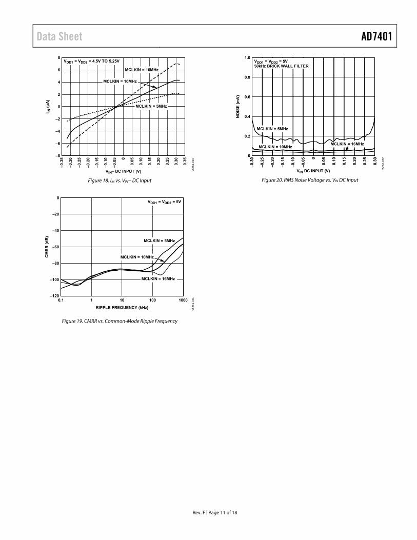
Figure 18. IIN vs. VIN− DC Input
0
–1200.1 1000
RIPPLE FREQUENCY (kHz)
CM
RR
(d
B)
–20
–40
–60
–80
–100
1 10 100
VDD1 = V DD2 = 5 VVDD1 = VDD2 = 5V
MCLKIN = 16MHz
MCLKIN = 5MHz
MCLKIN = 10MHz
0585
1-03
1
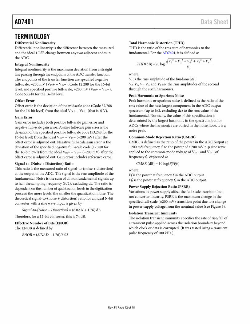
Figure 19. CMRR vs. Common-Mode Ripple Frequency
1.0
0
VIN DC INPUT (V)
NO
ISE
(m
V)
0.8
0.6
0.4
0.2
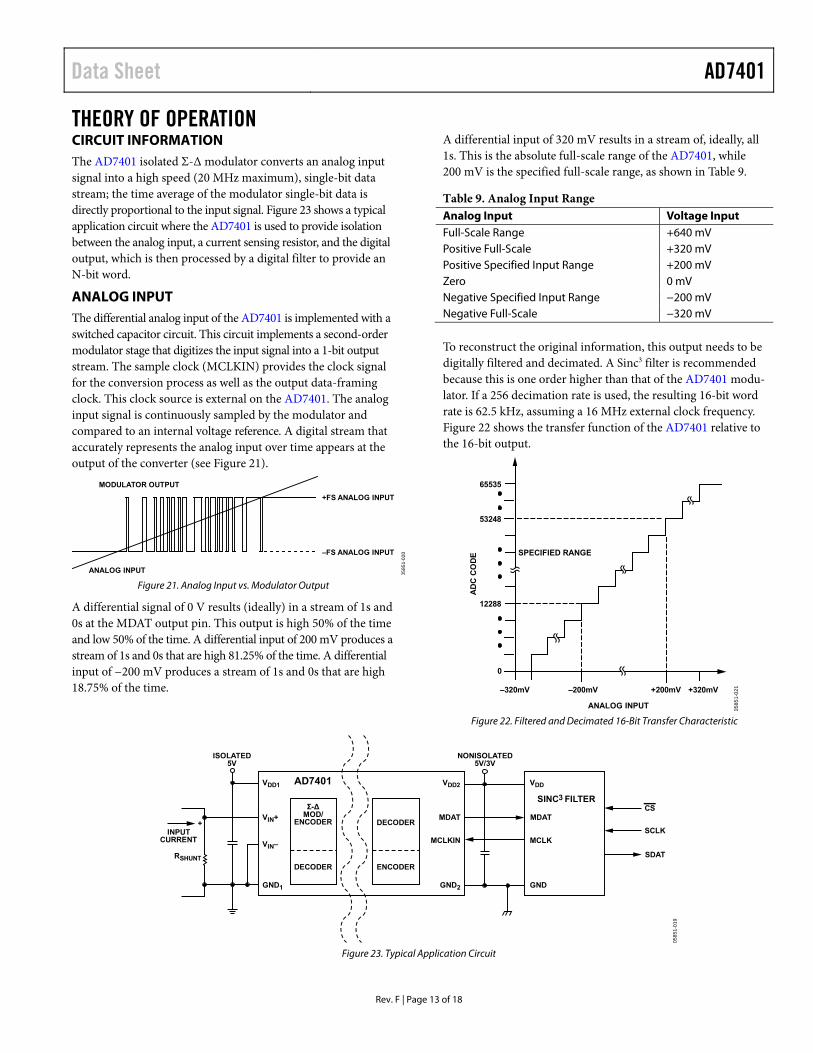
VDD1 = VDD2 = 5V50kHz BRICK WALL FILTER
MCLKIN = 5MHz
MCLKIN = 10MHzMCLKIN = 16MHz
0585
1-03
2
–0.3
0
–0.2
5
–0.2
0
–0.1
5
–0.1
0
–0.0
5 0
0.05
0.10
0.15
0.20
0.25
0.30
Figure 20. RMS Noise Voltage vs. VIN DC Input
AD7401 Data Sheet
Rev. F | Page 12 of 18
TERMINOLOGY Differential Nonlinearity Differential nonlinearity is the difference between the measured and the ideal 1 LSB change between any two adjacent codes in the ADC.
Integral Nonlinearity Integral nonlinearity is the maximum deviation from a straight line passing through the endpoints of the ADC transfer function. The endpoints of the transfer function are specified negative full-scale, −200 mV (VIN+ − VIN−), Code 12,288 for the 16-bit level, and specified positive full-scale, +200 mV (VIN+ − VIN−), Code 53,248 for the 16-bit level.
Offset Error Offset error is the deviation of the midscale code (Code 32,768 for the 16-bit level) from the ideal VIN+ − VIN− (that is, 0 V).
Gain Error Gain error includes both positive full-scale gain error and negative full-scale gain error. Positive full-scale gain error is the deviation of the specified positive full-scale code (53,248 for the 16-bit level) from the ideal VIN+ − VIN− (+200 mV) after the offset error is adjusted out. Negative full-scale gain error is the deviation of the specified negative full-scale code (12,288 for the 16-bit level) from the ideal VIN+ − VIN− (−200 mV) after the offset error is adjusted out. Gain error includes reference error.
Signal-to-(Noise + Distortion) Ratio This ratio is the measured ratio of signal-to-(noise + distortion) at the output of the ADC. The signal is the rms amplitude of the fundamental. Noise is the sum of all nonfundamental signals up to half the sampling frequency (fS/2), excluding dc. The ratio is dependent on the number of quantization levels in the digitization process; the more levels, the smaller the quantization noise. The theoretical signal-to-(noise + distortion) ratio for an ideal N-bit converter with a sine wave input is given by
Signal-to-(Noise + Distortion) = (6.02 N + 1.76) dB
Therefore, for a 12-bit converter, this is 74 dB.
Effective Number of Bits (ENOB) The ENOB is defined by
ENOB = (SINAD − 1.76)/6.02
Total Harmonic Distortion (THD) THD is the ratio of the rms sum of harmonics to the fundamental. For the AD7401, it is defined as
1
65432
VVVVVV
THD22222
log20)dB(++++
=
where: V1 is the rms amplitude of the fundamental. V2, V3, V4, V5, and V6 are the rms amplitudes of the second through the sixth harmonics.
Peak Harmonic or Spurious Noise Peak harmonic or spurious noise is defined as the ratio of the rms value of the next largest component in the ADC output spectrum (up to fS/2, excluding dc) to the rms value of the fundamental. Normally, the value of this specification is determined by the largest harmonic in the spectrum, but for ADCs where the harmonics are buried in the noise floor, it is a noise peak.
Common-Mode Rejection Ratio (CMRR) CMRR is defined as the ratio of the power in the ADC output at ±200 mV frequency, f, to the power of a 200 mV p-p sine wave applied to the common-mode voltage of VIN+ and VIN− of frequency fS, expressed as
CMRR (dB) = 10 log(Pf/PfS)
where: Pf is the power at frequency f in the ADC output. PfS is the power at frequency fS in the ADC output.
Power Supply Rejection Ratio (PSRR) Variations in power supply affect the full-scale transition but not converter linearity. PSRR is the maximum change in the specified full-scale (±200 mV) transition point due to a change in power supply voltage from the nominal value (see Figure 6).
Isolation Transient Immunity The isolation transient immunity specifies the rate of rise/fall of a transient pulse applied across the isolation boundary beyond which clock or data is corrupted. (It was tested using a transient pulse frequency of 100 kHz.)
Data Sheet AD7401
Rev. F | Page 13 of 18
THEORY OF OPERATION CIRCUIT INFORMATION The AD7401 isolated Σ-Δ modulator converts an analog input signal into a high speed (20 MHz maximum), single-bit data stream; the time average of the modulator single-bit data is directly proportional to the input signal. Figure 23 shows a typical application circuit where the AD7401 is used to provide isolation between the analog input, a current sensing resistor, and the digital output, which is then processed by a digital filter to provide an N-bit word.
ANALOG INPUT The differential analog input of the AD7401 is implemented with a switched capacitor circuit. This circuit implements a second-order modulator stage that digitizes the input signal into a 1-bit output stream. The sample clock (MCLKIN) provides the clock signal for the conversion process as well as the output data-framing clock. This clock source is external on the AD7401. The analog input signal is continuously sampled by the modulator and compared to an internal voltage reference. A digital stream that accurately represents the analog input over time appears at the output of the converter (see Figure 21).
MODULATOR OUTPUT
+FS ANALOG INPUT
–FS ANALOG INPUT
ANALOG INPUT 0585
1-02
0
Figure 21. Analog Input vs. Modulator Output
A differential signal of 0 V results (ideally) in a stream of 1s and 0s at the MDAT output pin. This output is high 50% of the time and low 50% of the time. A differential input of 200 mV produces a stream of 1s and 0s that are high 81.25% of the time. A differential input of −200 mV produces a stream of 1s and 0s that are high 18.75% of the time.
A differential input of 320 mV results in a stream of, ideally, all 1s. This is the absolute full-scale range of the AD7401, while 200 mV is the specified full-scale range, as shown in Table 9.
Table 9. Analog Input Range Analog Input Voltage Input Full-Scale Range +640 mV Positive Full-Scale +320 mV Positive Specified Input Range +200 mV Zero 0 mV Negative Specified Input Range −200 mV Negative Full-Scale −320 mV
To reconstruct the original information, this output needs to be digitally filtered and decimated. A Sinc3 filter is recommended because this is one order higher than that of the AD7401 modu-lator. If a 256 decimation rate is used, the resulting 16-bit word rate is 62.5 kHz, assuming a 16 MHz external clock frequency. Figure 22 shows the transfer function of the AD7401 relative to the 16-bit output.
65535
53248
SPECIFIED RANGE
ANALOG INPUT
AD
C C
OD
E
12288
–320mV –200mV +200mV +320mV
0
0585
1-02
1
Figure 22. Filtered and Decimated 16-Bit Transfer Characteristic
Σ-∆MOD/
ENCODERINPUT
CURRENT
NONISOLATED5V/3V
ISOLATED5V
VDD1
RSHUNT
VIN+
VIN–
GND1
VDD
GND
VDD2
MDAT MDAT
SINC3 FILTER
AD7401
MCLKIN
SDAT
CS
SCLKMCLK
GND2
DECODER
DECODER+
ENCODER
0585
1-01
9
Figure 23. Typical Application Circuit
AD7401 Data Sheet
Rev. F | Page 14 of 18
DIFFERENTIAL INPUTS The analog input to the modulator is a switched capacitor design. The analog signal is converted into charge by highly linear sampling capacitors. A simplified equivalent circuit diagram of the analog input is shown in Figure 24. A signal source driving the analog input must be able to provide the charge onto the sampling capacitors every half MCLKIN cycle and settle to the required accuracy within the next half cycle.
φA
φB1kΩ
VIN–
φA
φB
φB φB
1kΩVIN+ 2pF
2pF
φA φAMCLKIN 0585
1-02
2
Figure 24. Analog Input Equivalent Circuit
Because the AD7401 samples the differential voltage across its analog inputs, low noise performance is attained with an input circuit that provides low common-mode noise at each input. The amplifiers used to drive the analog inputs play a critical role in attaining the high performance available from the AD7401.
When a capacitive load is switched onto the output of an operational amplifier, the amplitude momentarily drops. The operational amplifier tries to correct the situation and, in the process, hits its slew rate limit. This nonlinear response, which can cause excessive ringing, can lead to distortion. To remedy the situation, a low-pass RC filter can be connected between the amplifier and the input to the AD7401. The external capacitor at each input aids in supplying the current spikes created during the sampling process, and the resistor isolates the operational amplifier from the transient nature of the load.
The recommended circuit configuration for driving the differential inputs to achieve best performance is shown in Figure 25. A capacitor between the two input pins sources or sinks charge to allow most of the charge that is needed by one input to be effectively supplied by the other input. The series resistor again isolates any operational amplifier from the current spikes created during the sampling process. Recommended values for the resistors and capacitor are 22 Ω and 47 pF, respectively.
RVIN–
RVIN+
C AD7401
0585
1-02
3
Figure 25. Differential Input RC Network
Data Sheet AD7401
Rev. F | Page 15 of 18
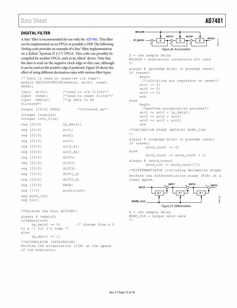
DIGITAL FILTER A Sinc3 filter is recommended for use with the AD7401. This filter can be implemented on an FPGA or possibly a DSP. The following Verilog code provides an example of a Sinc3 filter implementation on a Xylinx® Spartan-II 2.5 V FPGA. This code can possibly be compiled for another FPGA, such as an Altera® device. Note that the data is read on the negative clock edge in this case, although it can be read on the positive edge if preferred. Figure 29 shows the effect of using different decimation rates with various filter types.
/*`Data is read on negative clk edge*/ module DEC256SINC24B(mdata1, mclk1, reset, DATA);
input mclk1; /*used to clk filter*/ input reset; /*used to reset filter*/ input mdata1; /*ip data to be filtered*/
output [15:0] DATA; /*filtered op*/
integer location; integer info_file;
reg [23:0] ip_data1;
reg [23:0] acc1;
reg [23:0] acc2;
reg [23:0] acc3;
reg [23:0] acc3_d1;
reg [23:0] acc3_d2;
reg [23:0] diff1;
reg [23:0] diff2;
reg [23:0] diff3;
reg [23:0] diff1_d;
reg [23:0] diff2_d;
reg [15:0] DATA;
reg [7:0] word_count;
reg word_clk; reg init;
/*Perform the Sinc ACTION*/
always @ (mdata1) if(mdata1==0) ip_data1 <= 0; /* change from a 0 to a -1 for 2's comp */ else ip_data1 <= 1;
/*ACCUMULATOR (INTEGRATOR) Perform the accumulation (IIR) at the speed of the modulator.
MCLKIN
IP_DATA1
ACC1+ ACC2+ACC3+
+Z
+Z
+Z
0585
1-02
4
Figure 26. Accumulator
Z = one sample delay MCLKIN = modulators conversion bit rate */
always @ (posedge mclk1 or posedge reset) if (reset) begin /*initialize acc registers on reset*/ acc1 <= 0; acc2 <= 0; acc3 <= 0; end else begin /*perform accumulation process*/ acc1 <= acc1 + ip_data1; acc2 <= acc2 + acc1; acc3 <= acc3 + acc2; end
/*DECIMATION STAGE (MCLKIN/ WORD_CLK) */
always @ (negedge mclk1 or posedge reset) if (reset) word_count <= 0; else word_count <= word_count + 1;
always @ (word_count) word_clk <= word_count[7];
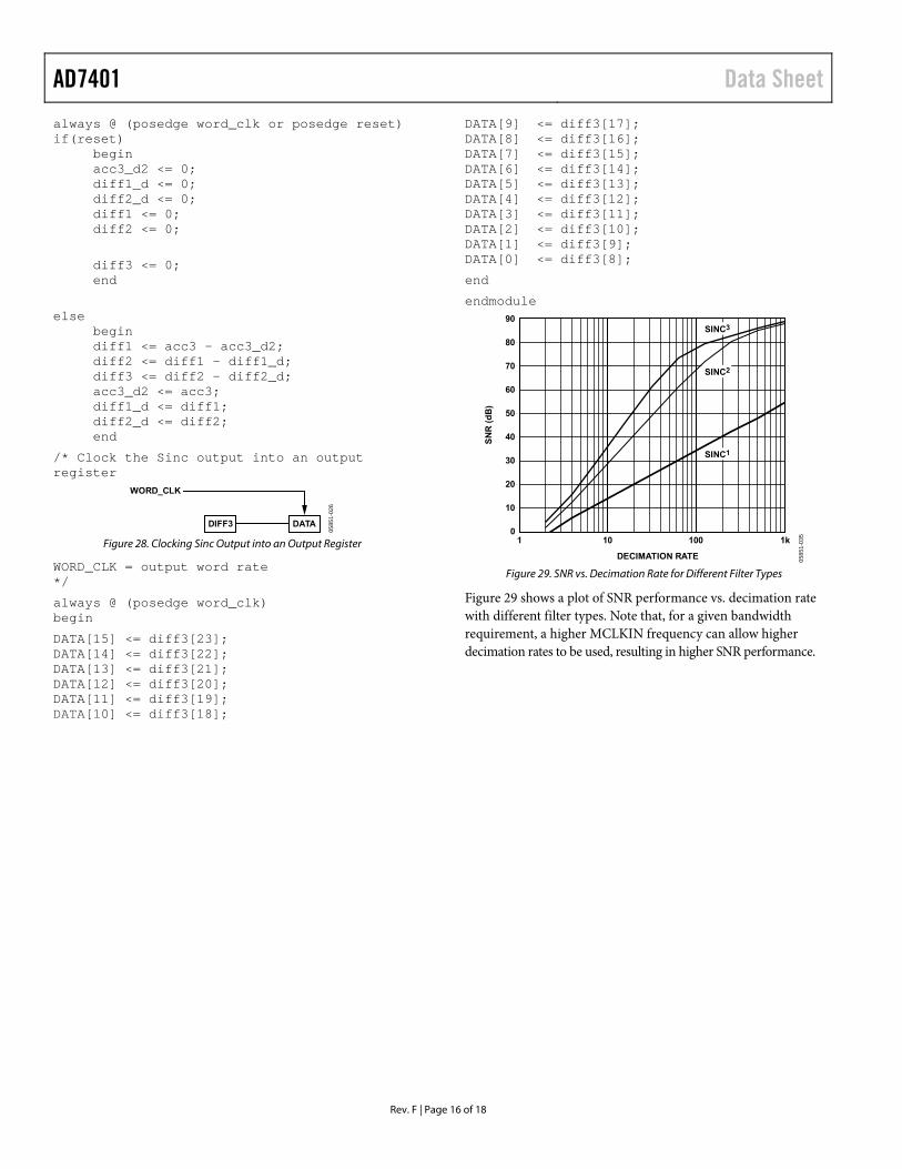
/*DIFFERENTIATOR (including decimation stage)
Perform the differentiation stage (FIR) at a lower speed.
WORD_CLK
ACC3DIFF1 DIFF3+
–
+
–
DIFF2
Z–1–
+
–Z–1 Z–1
0585
1-02
5
Figure 27. Differentiator
Z = one sample delay WORD_CLK = output word rate */
AD7401 Data Sheet
Rev. F | Page 16 of 18
always @ (posedge word_clk or posedge reset) if(reset) begin acc3_d2 <= 0; diff1_d <= 0; diff2_d <= 0; diff1 <= 0; diff2 <= 0;
diff3 <= 0; end
else begin diff1 <= acc3 - acc3_d2; diff2 <= diff1 - diff1_d; diff3 <= diff2 - diff2_d; acc3_d2 <= acc3; diff1_d <= diff1; diff2_d <= diff2; end
/* Clock the Sinc output into an output register
WORD_CLK
DATADIFF3
0585
1-02
6
Figure 28. Clocking Sinc Output into an Output Register
WORD_CLK = output word rate */
always @ (posedge word_clk) begin
DATA[15] <= diff3[23]; DATA[14] <= diff3[22]; DATA[13] <= diff3[21]; DATA[12] <= diff3[20]; DATA[11] <= diff3[19]; DATA[10] <= diff3[18];
DATA[9] <= diff3[17]; DATA[8] <= diff3[16]; DATA[7] <= diff3[15]; DATA[6] <= diff3[14]; DATA[5] <= diff3[13]; DATA[4] <= diff3[12]; DATA[3] <= diff3[11]; DATA[2] <= diff3[10]; DATA[1] <= diff3[9]; DATA[0] <= diff3[8];
end
endmodule
80
70
60
50
40
30
20
10
0
90
10 100 1k1
DECIMATION RATE
SN
R (
dB
)
SINC3
SINC2
SINC1
0585
1-03
5
Figure 29. SNR vs. Decimation Rate for Different Filter Types
Figure 29 shows a plot of SNR performance vs. decimation rate with different filter types. Note that, for a given bandwidth requirement, a higher MCLKIN frequency can allow higher decimation rates to be used, resulting in higher SNR performance.

Data Sheet AD7401
Rev. F | Page 17 of 18
APPLICATIONS INFORMATION GROUNDING AND LAYOUT Supply decoupling with a value of 100 nF is strongly recom-mended on both VDD1 and VDD2. Decoupling on one or both VDD1 pins does not affect performance significantly. In applications involving high common-mode transients, care must be taken to ensure that board coupling across the isolation barrier is mini-mized. Furthermore, the board layout must be designed so any coupling that occurs equally affects all pins on a given component side. Failure to ensure this may cause voltage differentials between pins to exceed the absolute maximum ratings of the device, thereby leading to latch-up or permanent damage. Any decoupling used must be placed as close to the supply pins as possible.
Series resistance in the analog inputs must be minimized to avoid any distortion effects, especially at high temperatures. If possible, equalize the source impedance on each analog input to minimize offset. Beware of mismatch and thermocouple effects on the analog input PCB tracks to reduce offset drift.
EVALUATING THE AD7401 PERFORMANCE A simple standalone AD7401 evaluation board is available with split ground planes and a board split beneath the AD7401 package to ensure isolation. This board allows access to each pin on the device for evaluation purposes. External supplies and all other circuitry (such as a digital filter) must be provided by the user.
INSULATION LIFETIME All insulation structures, subjected to sufficient time and/or voltage, are vulnerable to breakdown. In addition to the testing performed by the regulatory agencies, Analog Devices has carried out an extensive set of evaluations to determine the lifetime of the insulation structure within the AD7401.
These tests subject populations of devices to continuous cross isolation voltages. To accelerate the occurrence of failures, the selected test voltages are values exceeding those of normal use. The time to failure values of these units are recorded and used to calculate acceleration factors. These factors are then used to calculate the time to failure under normal operating conditions. The values shown in Table 7 are the lesser of the following two values:
• The value that ensures at least a 50-year lifetime of continuous use
• The maximum CSA/VDE approved working voltage
Note that the lifetime of the AD7401 varies according to the waveform type imposed across the isolation barrier. The iCoupler insulation structure is stressed differently depending on whether the waveform is bipolar ac, unipolar ac, or dc. Figure 30, Figure 31, and Figure 32 illustrate the different isolation voltage waveforms.
0V
RATED PEAK VOLTAGE
0585
1-03
9
Figure 30. Bipolar AC Waveform
0V
RATED PEAK VOLTAGE
0585
1-04
0
Figure 31. Unipolar AC Waveform
0V
RATED PEAK VOLTAGE
0585
1-04
1
Figure 32. DC Waveform
AD7401 Data Sheet
Rev. F | Page 18 of 18
OUTLINE DIMENSIONS
CONTROLLING DIMENSIONS ARE IN MILLIMETERS; INCH DIMENSIONS(IN PARENTHESES) ARE ROUNDED-OFF MILLIMETER EQUIVALENTS FORREFERENCE ONLY AND ARE NOT APPROPRIATE FOR USE IN DESIGN.
COMPLIANT TO JEDEC STANDARDS MS-013-AA
10.50 (0.4134)10.10 (0.3976)
0.30 (0.0118)0.10 (0.0039)
2.65 (0.1043)2.35 (0.0925)
10.65 (0.4193)10.00 (0.3937)
7.60 (0.2992)7.40 (0.2913)
0.75 (0.0295)0.25 (0.0098)
45°
1.27 (0.0500)0.40 (0.0157)
COPLANARITY0.10 0.33 (0.0130)
0.20 (0.0079)
0.51 (0.0201)0.31 (0.0122)
SEATINGPLANE
8°0°
16 9
81
1.27 (0.0500)BSC
03-2
7-2
007-
B
Figure 33. 16-Lead Standard Small Outline Package [SOIC_W]
Wide Body (RW-16)
Dimensions shown in millimeters and (inches)
ORDERING GUIDE Model1 Temperature Range Package Description Package Option AD7401YRWZ −40°C to +105°C 16-Lead Standard Small Outline Package [SOIC_W] RW-16 AD7401YRWZ-REEL −40°C to +105°C 16-Lead Standard Small Outline Package [SOIC_W] RW-16 AD7401YRWZ-REEL7 −40°C to +105°C 16-Lead Standard Small Outline Package [SOIC_W] RW-16 EVAL-AD7401EDZ Evaluation Board EVAL-CED1Z Development Board 1 Z = RoHS Compliant Part.
©2006–2018 Analog Devices, Inc. All rights reserved. Trademarks and registered trademarks are the property of their respective owners. D05851-0-4/18(F)