Embed Size (px)
Citation preview
© Semiconductor Components Industries, LLC, 2016
August, 2019 − Rev. 11 Publication Order Number:
ISL9V3040−F085C//D
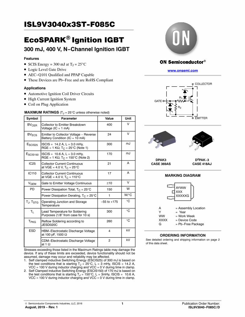
ISL9V3040x3ST-F085C
EcoSPARK� Ignition IGBT
300 mJ, 400 V, N−Channel Ignition IGBT
Features
• SCIS Energy = 300 mJ at TJ = 25°C• Logic Level Gate Drive• AEC−Q101 Qualified and PPAP Capable• These Devices are Pb−Free and are RoHS Compliant
Applications
• Automotive Ignition Coil Driver Circuits• High Current Ignition System• Coil on Plug Application
MAXIMUM RATINGS (TJ = 25°C unless otherwise noted)
Symbol Parameter Value Unit
BVCER Collector to Emitter Breakdown Voltage (IC = 1 mA)
400 V
BVECS Emitter to Collector Voltage − ReverseBattery Condition (IC = 10 mA)
24 V
ESCIS25 ISCIS = 14.2 A, L = 3.0 mHy, RGE = 1 K�, TC = 25°C (Note 1)
300 mJ
ESCIS150 ISCIS = 10.6 A, L = 3.0 mHy, RGE = 1 K�, TC = 150°C (Note 2)
170 mJ
IC25 Collector Current Continuous at VGE = 4.0 V, TC = 25°C
21 A
IC110 Collector Current Continuous at VGE = 4.0 V, TC = 110°C
17 A
VGEM Gate to Emitter Voltage Continuous ±10 V
PD Power Dissipation Total, TC = 25°C 150 W
Power Dissipation Derating, TC > 25°C 1 W/°C
TJ, TSTG Operating Junction and Storage Temperature
−55 to +175 °C
TL Lead Temperature for Soldering Purposes (1/8” from case for 10 s)
300 °C
TPKG Reflow Soldering according toJESD020C
260 °C
ESD HBM−Electrostatic Discharge Voltageat 100 pF, 1500 �
4 kV
CDM−Electrostatic Discharge Voltageat 1 �
2 kV
Stresses exceeding those listed in the Maximum Ratings table may damage thedevice. If any of these limits are exceeded, device functionality should not beassumed, damage may occur and reliability may be affected.1. Self clamped inductive Switching Energy (ESCIS25) of 300 mJ is based on
the test conditions that is starting TJ = 25°C, L = 3 mHy, ISCIS = 14.2 A,VCC = 100 V during inductor charging and VCC = 0 V during time in clamp.
2. Self Clamped inductive Switching Energy (ESCIS150) of 170 mJ is based onthe test conditions that is starting TJ = 150°C, L = 3mHy, ISCIS = 10.6 A,VCC = 100 V during inductor charging and VCC = 0 V during time in clamp.
DPAK3CASE 369AS
See detailed ordering and shipping information on page 2of this data sheet.
ORDERING INFORMATION
www.onsemi.com
MARKING DIAGRAM
A = Assembly LocationY = YearWW = Work WeekXXXX = Device CodeG = Pb−Free Package
AYWWXXXXXXXXG
GATE
COLLECTOR
EMITTER
R1
R2
D2PAK−3CASE 418AJ
ISL9V3040x3ST−F085C
www.onsemi.com2
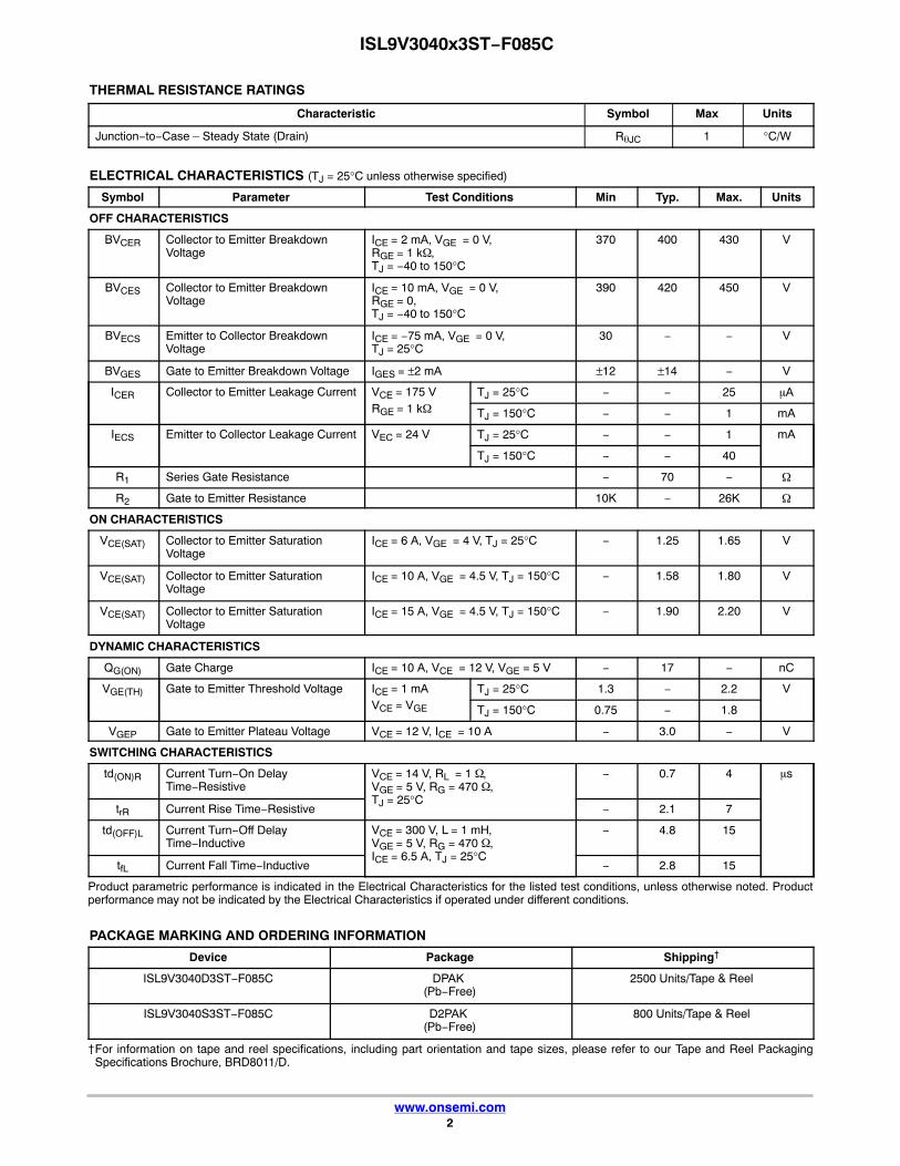
THERMAL RESISTANCE RATINGS
Characteristic Symbol Max Units
Junction−to−Case – Steady State (Drain) R�JC 1 °C/W
ELECTRICAL CHARACTERISTICS (TJ = 25°C unless otherwise specified)
Symbol Parameter Test Conditions Min Typ. Max. Units
OFF CHARACTERISTICS
BVCER Collector to Emitter Breakdown Voltage
ICE = 2 mA, VGE = 0 V,RGE = 1 k�,TJ = −40 to 150°C
370 400 430 V
BVCES Collector to Emitter Breakdown Voltage
ICE = 10 mA, VGE = 0 V,RGE = 0,TJ = −40 to 150°C
390 420 450 V
BVECS Emitter to Collector Breakdown Voltage
ICE = −75 mA, VGE = 0 V,TJ = 25°C
30 − − V
BVGES Gate to Emitter Breakdown Voltage IGES = ±2 mA ±12 ±14 − V
ICER Collector to Emitter Leakage Current VCE = 175 VRGE = 1 k�
TJ = 25°C − − 25 �A
TJ = 150°C − − 1 mA
IECS Emitter to Collector Leakage Current VEC = 24 V TJ = 25°C − − 1 mA
TJ = 150°C − − 40
R1 Series Gate Resistance − 70 − �
R2 Gate to Emitter Resistance 10K − 26K �
ON CHARACTERISTICS
VCE(SAT) Collector to Emitter Saturation Voltage
ICE = 6 A, VGE = 4 V, TJ = 25°C − 1.25 1.65 V
VCE(SAT) Collector to Emitter Saturation Voltage
ICE = 10 A, VGE = 4.5 V, TJ = 150°C − 1.58 1.80 V
VCE(SAT) Collector to Emitter Saturation Voltage
ICE = 15 A, VGE = 4.5 V, TJ = 150°C − 1.90 2.20 V
DYNAMIC CHARACTERISTICS
QG(ON) Gate Charge ICE = 10 A, VCE = 12 V, VGE = 5 V − 17 − nC
VGE(TH) Gate to Emitter Threshold Voltage ICE = 1 mAVCE = VGE
TJ = 25°C 1.3 − 2.2 V
TJ = 150°C 0.75 − 1.8
VGEP Gate to Emitter Plateau Voltage VCE = 12 V, ICE = 10 A − 3.0 − V
SWITCHING CHARACTERISTICS
td(ON)R Current Turn−On Delay Time−Resistive
VCE = 14 V, RL = 1 �,VGE = 5 V, RG = 470 �,TJ = 25°C
− 0.7 4 �s
trR Current Rise Time−Resistive − 2.1 7
td(OFF)L Current Turn−Off Delay Time−Inductive
VCE = 300 V, L = 1 mH,VGE = 5 V, RG = 470 �,ICE = 6.5 A, TJ = 25°C
− 4.8 15
tfL Current Fall Time−Inductive − 2.8 15
Product parametric performance is indicated in the Electrical Characteristics for the listed test conditions, unless otherwise noted. Productperformance may not be indicated by the Electrical Characteristics if operated under different conditions.
PACKAGE MARKING AND ORDERING INFORMATION
Device Package Shipping†
ISL9V3040D3ST−F085C DPAK (Pb−Free)
2500 Units/Tape & Reel
ISL9V3040S3ST−F085C D2PAK (Pb−Free)
800 Units/Tape & Reel
†For information on tape and reel specifications, including part orientation and tape sizes, please refer to our Tape and Reel PackagingSpecifications Brochure, BRD8011/D.
ISL9V3040x3ST−F085C
www.onsemi.com3
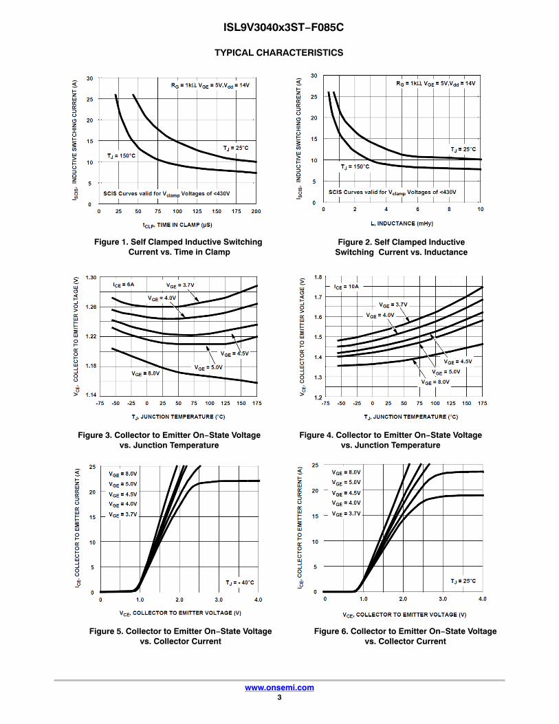
TYPICAL CHARACTERISTICS
Figure 1. Self Clamped Inductive Switching Current vs. Time in Clamp
Figure 2. Self Clamped InductiveSwitching Current vs. Inductance
Figure 3. Collector to Emitter On−State Voltagevs. Junction Temperature
Figure 4. Collector to Emitter On−State Voltagevs. Junction Temperature
Figure 5. Collector to Emitter On−State Voltagevs. Collector Current
Figure 6. Collector to Emitter On−State Voltagevs. Collector Current
ISL9V3040x3ST−F085C
www.onsemi.com4
TYPICAL CHARACTERISTICS (continued)
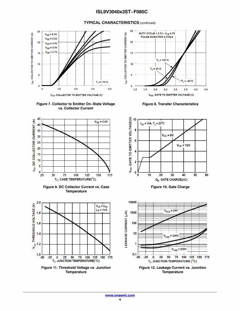
Figure 7. Collector to Emitter On−State Voltagevs. Collector Current
Figure 8. Transfer Characteristics
Figure 9. DC Collector Current vs. CaseTemperature
Figure 10. Gate Charge
Figure 11. Threshold Voltage vs. JunctionTemperature
Figure 12. Leakage Current vs. JunctionTemperature
ISL9V3040x3ST−F085C
www.onsemi.com5
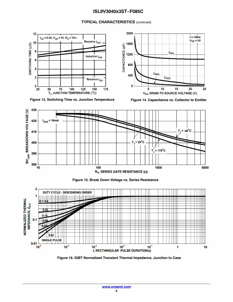
Figure 13. Switching Time vs. Junction Temperature Figure 14. Capacitance vs. Collector to Emitter
Figure 15. Break Down Voltage vs. Series Resistance
TYPICAL CHARACTERISTICS (continued)
Figure 16. IGBT Normalized Transient Thermal Impedance, Junction to Case
ISL9V3040x3ST−F085C
www.onsemi.com6
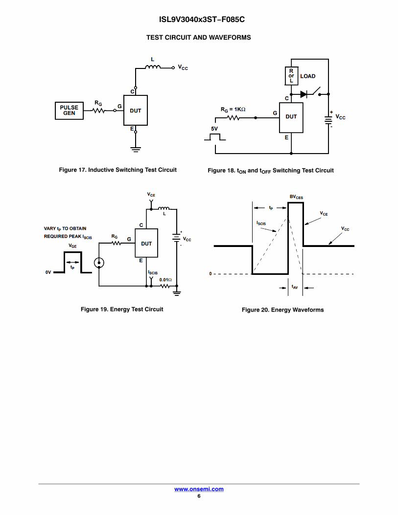
Figure 17. Inductive Switching Test Circuit Figure 18. tON and tOFF Switching Test Circuit
TEST CIRCUIT AND WAVEFORMS
Figure 19. Energy Test Circuit Figure 20. Energy Waveforms
ISL9V3040x3ST−F085C
www.onsemi.com7
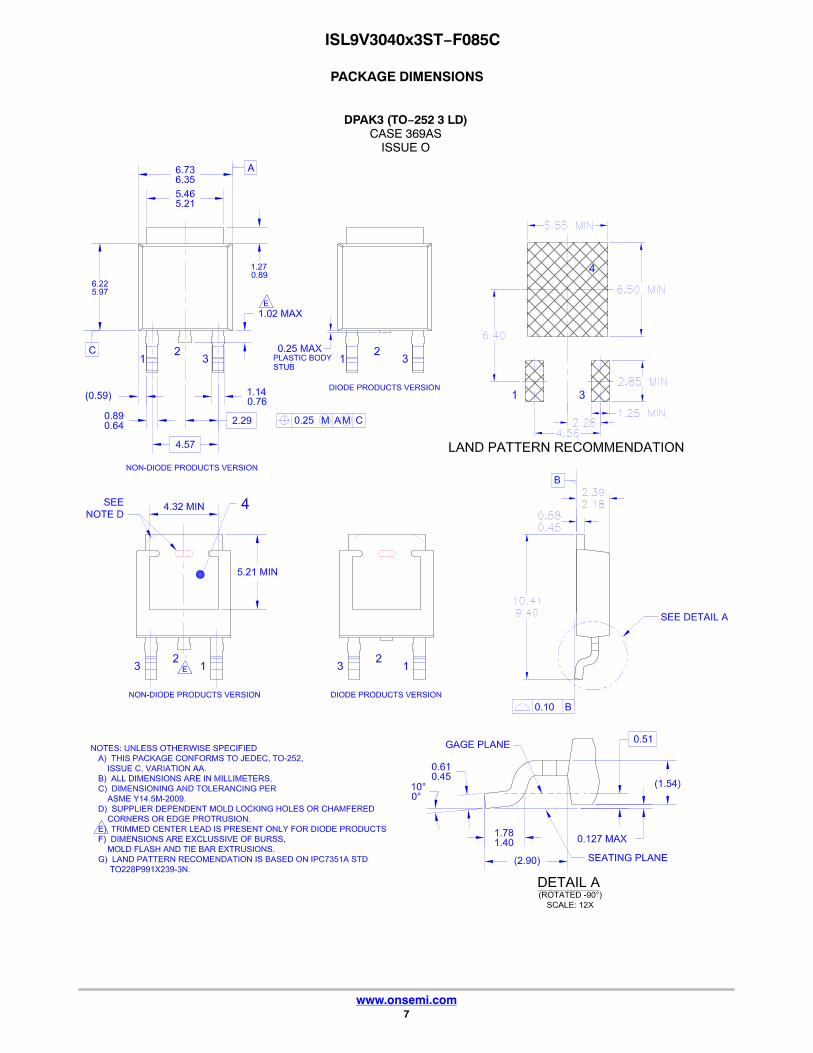
PACKAGE DIMENSIONS
DPAK3 (TO−252 3 LD)CASE 369AS
ISSUE O

ISL9V3040x3ST−F085C
www.onsemi.com8
PACKAGE DIMENSIONS
D2PAK−3 (TO−263, 3−LEAD)CASE 418AJ
ISSUE C
DIM MIN MAX MIN MAXMILLIMETERSINCHES
D 0.330 0.380 8.38 9.65
E 0.380 0.420 9.65 10.67
A 0.160 0.190 4.06 4.83
b 0.020 0.039 0.51 0.99
c2 0.045 0.065 1.14 1.65
e 0.100 BSC 2.54 BSC
A1 0.000 0.010 0.00 0.25
c 0.012 0.029 0.30 0.74
L 0.070 0.110 1.78 2.79H 0.575 0.625 14.60 15.88
L2 −−−− 0.070 −−−− 1.78
NOTES:1. DIMENSIONING AND TOLERANCING PER ASME
Y14.5M, 1994.2. CONTROLLING DIMENSION: INCHES.3. CHAMFER OPTIONAL4. DIMENSIONS D AND E DO NOT INCLUDE MOLD
FLASH. MOLD FLASH SHALL NOT EXCEED 0.005PER SIDE. THESE DIMENSIONS ARE MEASUREDAT THE OUTERMOST EXTREMES OF THE PLAS-TIC BODY AT DATUM H.
5. THERMAL PAD CONTOUR IS OPTIONAL WITHINDIMENSIONS E, L1, D1 AND E1.
E1 0.245 −−−− 6.22 −−−−
L1 −−−− 0.066 −−−− 1.68
D1 0.260 −−−− 6.60 −−−−
L3 0.010 BSC 0.25 BSCM −8 8 −8 8° ° ° °
E
DH
L1
b
e
A1B
H
L
M DETAIL C
SEATINGPLANE
A
2X
MAM0.10 B
c2
c
A
B SEATINGPLANE
DETAIL C
VIEW A−ASIDE VIEW
TOP VIEW
E2
L2
A
A
VIEW A−A
E1
D1
L1
OPTIONAL CONSTRUCTIONS
L3
GAUGEPLANE
NOTE 3
MAM0.10 B
*For additional information on our Pb−Free strategy and solderingdetails, please download the ON Semiconductor Soldering andMounting Techniques Reference Manual, SOLDERRM/D.
RECOMMENDED
0.366
0.100
DIMENSIONS: INCHES
PITCH
2X
0.653
0.0632X
0.436
0.169
SOLDERING FOOTPRINT*
ISL9V3040x3ST−F085C
www.onsemi.com9
ON Semiconductor and are trademarks of Semiconductor Components Industries, LLC dba ON Semiconductor or its subsidiaries in the United States and/or other countries.ON Semiconductor owns the rights to a number of patents, trademarks, copyrights, trade secrets, and other intellectual property. A listing of ON Semiconductor’s product/patentcoverage may be accessed at www.onsemi.com/site/pdf/Patent−Marking.pdf. ON Semiconductor reserves the right to make changes without further notice to any products herein.ON Semiconductor makes no warranty, representation or guarantee regarding the suitability of its products for any particular purpose, nor does ON Semiconductor assume any liabilityarising out of the application or use of any product or circuit, and specifically disclaims any and all liability, including without limitation special, consequential or incidental damages.Buyer is responsible for its products and applications using ON Semiconductor products, including compliance with all laws, regulations and safety requirements or standards,regardless of any support or applications information provided by ON Semiconductor. “Typical” parameters which may be provided in ON Semiconductor data sheets and/orspecifications can and do vary in different applications and actual performance may vary over time. All operating parameters, including “Typicals” must be validated for each customerapplication by customer’s technical experts. ON Semiconductor does not convey any license under its patent rights nor the rights of others. ON Semiconductor products are notdesigned, intended, or authorized for use as a critical component in life support systems or any FDA Class 3 medical devices or medical devices with a same or similar classificationin a foreign jurisdiction or any devices intended for implantation in the human body. Should Buyer purchase or use ON Semiconductor products for any such unintended or unauthorizedapplication, Buyer shall indemnify and hold ON Semiconductor and its officers, employees, subsidiaries, affiliates, and distributors harmless against all claims, costs, damages, andexpenses, and reasonable attorney fees arising out of, directly or indirectly, any claim of personal injury or death associated with such unintended or unauthorized use, even if suchclaim alleges that ON Semiconductor was negligent regarding the design or manufacture of the part. ON Semiconductor is an Equal Opportunity/Affirmative Action Employer. Thisliterature is subject to all applicable copyright laws and is not for resale in any manner.
PUBLICATION ORDERING INFORMATIONN. American Technical Support: 800−282−9855 Toll FreeUSA/Canada
Europe, Middle East and Africa Technical Support:Phone: 421 33 790 2910
ISL9V3040−F085C/D
ECOSPARK is registered trademark of Semiconductor Components Industries, LLC (SCILLC) or its subsidiaries in the United States and/or other countries.
LITERATURE FULFILLMENT:Literature Distribution Center for ON Semiconductor19521 E. 32nd Pkwy, Aurora, Colorado 80011 USAPhone: 303−675−2175 or 800−344−3860 Toll Free USA/CanadaFax: 303−675−2176 or 800−344−3867 Toll Free USA/CanadaEmail: [email protected]
ON Semiconductor Website: www.onsemi.com
Order Literature: http://www.onsemi.com/orderlit
For additional information, please contact your localSales Representative
◊
Mouser Electronics
Authorized Distributor
Click to View Pricing, Inventory, Delivery & Lifecycle Information: ON Semiconductor:
ISL9V3040D3ST-F085C ISL9V3040S3ST-F085C