Embed Size (px)
Citation preview
Integrated Silicon Solution, Inc. — www.issi.com — 1-800-379-4774 1Rev. E11/12/08
IS62WV1288ALL IS62WV1288BLL, IS65WV1288BLL
Copyright © 2005 Integrated Silicon Solution, Inc. All rights reserved. ISSI reserves the right to make changes to this specification and its products at any time without notice. ISSI assumes no liability arising out of the application or use of any information, products or services described herein. Customers are advised to obtain the lat-est version of this device specification before relying on any published information and before placing orders for products.
128K x 8 LOW VOLTAGE, ULTRA LOW POWER CMOS STATIC RAM
FEATURES
• High-speedaccesstime:45ns,55ns,70ns
• CMOSlowpoweroperation:
30 mW (typical) operating
15µW(typical)CMOSstandby
• TTLcompatibleinterfacelevels
• Singlepowersupply:
1.65V--2.2V Vdd (62WV1288ALL)
2.5V--3.6V Vdd (62WV1288BLL/ 65WV1288BLL)
• Fullystaticoperation:noclockorrefresh required
• Threestateoutputs
• AutomotiveandIndustrialtemperaturesavailable
• Lead-freeavailable
DESCRIPTION
The ISSI IS62WV1288ALL / IS62/65WV1288BLL arehigh-speed,1MbitstaticRAMsorganizedas128Kwordsby 8 bits. It is fabricated using ISSI's high-performance CMOStechnology.Thishighly reliableprocesscoupledwith innovative circuit design techniques, yields high-performance and low power consumption devices.
When CS1 isHIGH(deselected)orwhenCS2 isLOW (deselected), the device assumes a standby mode at which the power dissipation can be reduced down with CMOSinputlevels.
Easy memory expansion is provided by using Chip Enable andOutputEnableinputs.TheactiveLOWWriteEnable(WE) controls both writing and reading of the memory.
The IS62WV1288ALL and IS62/65WV1288BLL arepackagedintheJEDECstandard32-pinTSOP(TYPEI),sTSOP(TYPEI),SOP,and36-pinminiBGA.
FUNCTIONAL BLOCK DIAGRAM
DECEMBER 2008
A0-A16
CS1
OE
WE
128K x 8MEMORY ARRAYDECODER
COLUMN I/O
CONTROLCIRCUIT
GND
VDD
I/ODATA
CIRCUITI/O0-I/O7
CS2

2 Integrated Silicon Solution, Inc. — www.issi.com — 1-800-379-4774 Rev. E
11/12/08
IS62WV1288ALL, IS62WV1288BLL, IS65WV1288BLL
PIN DESCRIPTIONS
A0-A16 Address Inputs
CS1 Chip Enable 1 Input
CS2 Chip Enable 2 Input
OE OutputEnableInput
WE Write Enable Input
I/O0-I/O7 Input/Output
NC No Connection
Vdd Power
GND Ground
36-pin mini BGA (B) (6mm x 8mm) 32-pin TSOP (TYPE I) (T), 32-pin sTSOP (TYPE I) (H)
PIN CONFIGURATION
32-pin SOP (Q)
1 2 3 4 5 6
A
B
C
D
E
F
G
H
A0
I/O4
I/O5
GND
VDD
I/O6
I/O7
A9
A1
A2
OE
A10
CS2
WE
NC
NC
CS1
A11
A3
A4
A5
NC
A16
A12
A6
A7
A15
A13
A8
I/O0
I/O1
VDD
GND
I/O2
I/O3
A14
12345678910111213141516
32313029282726252423222120191817
A11A9A8
A13WE
CS2A15VDD
NCA16A14A12
A7A6A5A4
OEA10CS1I/O7I/O6I/O5I/O4I/O3GNDI/O2I/O1I/O0A0A1A2A3
1
2
3
4
5
6
7
8
9
10
11
12
13
14
15
16
32
31
30
29
28
27
26
25
24
23
22
21
20
19
18
17
NC
A16
A14
A12
A7
A6
A5
A4
A3
A2
A1
A0
I/O0
I/O1
I/O2
GND
VDD
A15
CS2
WE
A13
A8
A9
A11
OE
A10
CS1
I/O7
I/O6
I/O5
I/O4
I/O3

Integrated Silicon Solution, Inc. — www.issi.com — 1-800-379-4774 3Rev. E11/12/08
IS62WV1288ALL, IS62WV1288BLL, IS65WV1288BLL
DC ELECTRICAL CHARACTERISTICS (Over Operating Range)
Symbol Parameter Test Conditions Vdd Min. Max. Unit
Voh OutputHIGHVoltage Ioh = -0.1mA 1.65-2.2V 1.4 — V Ioh = -1mA 2.5-3.6V 2.2 — V
VoL OutputLOWVoltage IoL = 0.1mA 1.65-2.2V — 0.2 V IoL = 2.1mA 2.5-3.6V — 0.4 V
VIh(2) InputHIGHVoltage 1.65-2.2V 1.4 Vdd + 0.2 V 2.5-3.6V 2.2 Vdd + 0.3 V
VIL(1) InputLOWVoltage 1.65-2.2V –0.2 0.4 V 2.5-3.6V –0.2 0.6 V
ILI InputLeakage GND≤ VIn ≤ Vdd –1 1 µA
ILo OutputLeakage GND≤ Vout ≤ Vdd, OutputsDisabled –1 1 µANotes:1.Undershoot: –1.0V for pulse width less than 10 ns. Not 100% tested.2.Overshoot:Vdd + 1.0V for pulse width less than 10 ns. Not 100% tested.
ABSOLUTE MAXIMUM RATINGS(1)
Symbol Parameter Value Unit
Vterm TerminalVoltagewithRespecttoGND –0.2toVdd+0.3 V
Vdd Vdd RelatedtoGND –0.2to+3.8 V
tstg StorageTemperature –65to+150 °C
Pt PowerDissipation 1.0 WNote:1.StressgreaterthanthoselistedunderABSOLUTEMAXIMUMRATINGSmaycausepermanentdamagetothedevice.Thisisa
stress rating only and functional operation of the device at these or any other conditions above those indicated in the operational sections of this specification is not implied. Exposure to absolute maximum rating conditions for extended periods may affect reli-ability.
OPERATING RANGE (Vdd)
Range Ambient Temperature IS62WV1288ALL IS62/65WV1288BLL
Commercial 0°Cto+70°C 1.65V-2.2V 2.5V-3.6V
Industrial/A1 –40°Cto+85°C 1.65V-2.2V 2.5V-3.6V
Automotive –40°Cto+125°C 2.5V-3.6V
TRUTH TABLE Mode WE CS1 CS2 OE I/O Operation Vdd Current
NotSelected X H X X High-Z IsB1, IsB2
(Power-down) X X L X High-Z IsB1, IsB2 OutputDisabled H L H H High-Z Icc Read H L H L dout Icc Write L L H X dIn Icc

4 Integrated Silicon Solution, Inc. — www.issi.com — 1-800-379-4774 Rev. E
11/12/08
IS62WV1288ALL, IS62WV1288BLL, IS65WV1288BLL
AC TEST LOADS
Figure 1 Figure 2
CAPACITANCE(1)
Symbol Parameter Conditions Max. Unit
cIn Input Capacitance VIn = 0V 8 pF
cout Input/OutputCapacitance Vout = 0V 10 pF
Note:1.Testedinitiallyandafteranydesignorprocesschangesthatmayaffecttheseparameters.
AC TEST CONDITIONS
Parameter 62WV1288ALL 62/65WV1288BLL (Unit) (Unit)
InputPulseLevel 0.4VtoVdd-0.2V 0.4VtoVdd-0.3V
InputRiseandFallTimes 5ns 5ns
InputandOutputTiming Vref Vref andReferenceLevel
OutputLoad SeeFigures1and2 SeeFigures1and2
1.65V - 2.2V 2.5V - 3.6V
r1(Ω) 3070 3070
R2(Ω) 3150 3150
Vref 0.9V 1.5V
Vtm 1.8V 2.8V
R1
30 pFIncluding
jig andscope
R2
OUTPUT
VTM
R1
5 pFIncluding
jig andscope
R2
OUTPUT
VTM

Integrated Silicon Solution, Inc. — www.issi.com — 1-800-379-4774 5Rev. E11/12/08
IS62WV1288ALL, IS62WV1288BLL, IS65WV1288BLL
POWER SUPPLY CHARACTERISTICS(1) (OverOperatingRange)
1.65V - 2.2V
Symbol Parameter Test Conditions Max. Unit 70 ns Icc Vdd DynamicOperating Vdd = Max., Com. 8 mA Supply Current Iout = 0 mA, f = fmAx Ind. 8 typ.(2) 5 Icc1 OperatingSupply Vdd = Max., Com. 5 mA Current Iout = 0 mA, f = 0 Ind. 5 IsB1 TTLStandbyCurrent Vdd = Max., Com. 0.8 mA (TTLInputs) VIn = VIh or VIL Ind. 0.8 CS1 = VIh , CS2 = VIL, f=1MHz
IsB2 CMOSStandby Vdd = Max., Com. 10 µA Current(CMOSInputs) CS1 ≥ Vdd – 0.2V, Ind. 10 CS2 ≤ 0.2V, typ.(2) 5 VIn ≥ Vdd – 0.2V, or VIn ≤ 0.2V, f = 0
Note:1. At f = fmAx, address and data inputs are cycling at the maximum frequency, f = 0 means no input lines change.2.TypicalvaluesaremeasuredatVdd=1.8V,TA=25oC. Not 100% tested.
POWER SUPPLY CHARACTERISTICS(1) (OverOperatingRange)
2.5V - 3.6V
Symbol Parameter Test Conditions Max. Max. Unit 45ns 55 ns Icc VddDynamicOperating Vdd = Max., Com. 17 15 mA Supply Current Iout = 0 mA, f = fmAx Ind./A1 17 15 A3 35 typ.(2) 12 10 Icc1 OperatingSupply Vdd = Max., Com. 5 5 mA Current Iout = 0 mA, f = 0 Ind./A1 5 5 A3 7 IsB1 TTLStandbyCurrent Vdd = Max., Com. 0.8 0.8 mA (TTLInputs) VIn = VIh or VIL Ind./A1 0.8 0.8 CS1 = VIh , CS2 = VIL, A3 3 f=1MHz
IsB2 CMOSStandby Vdd = Max., Com. 10 10 µA Current(CMOSInputs) CS1 ≥ Vdd – 0.2V, Ind./A1 10 10 CS2 ≤ 0.2V, A3 75 VIn ≥ Vdd – 0.2V, or typ.(2) 5 5 VIn ≤ 0.2V, f = 0
Note:1. At f = fmAx, address and data inputs are cycling at the maximum frequency, f = 0 means no input lines change.2.TypicalvaluesaremeasuredatVdd=3.0V,TA=25oC. Not 100% tested.

6 Integrated Silicon Solution, Inc. — www.issi.com — 1-800-379-4774 Rev. E
11/12/08
IS62WV1288ALL, IS62WV1288BLL, IS65WV1288BLL
AC WAVEFORMS
READ CYCLE NO. 1(1,2) (Address Controlled) (CS1 = OE = VIL, cs2 = WE = VIh)
DATA VALIDPREVIOUS DATA VALID
tAA
tOHAtOHA
tRC
DOUT
ADDRESS
READ CYCLE SWITCHING CHARACTERISTICS(1) (OverOperatingRange)
45 ns 55 ns 70 ns Symbol Parameter Min. Max. Min. Max. Min. Max. Unit
trc ReadCycleTime 45 — 55 — 70 — ns
tAA AddressAccessTime — 45 — 55 — 70 ns
tohA OutputHoldTime 10 — 10 — 10 — ns
tAcs1/tAcs2 CS1/CS2AccessTime — 45 — 55 — 70 ns
tdoe OEAccessTime — 20 — 25 — 35 ns
thzoe(2) OEtoHigh-ZOutput 0 15 0 20 0 25 ns
tLzoe(2) OEtoLow-ZOutput 5 — 5 — 5 — ns
thzcs1/thzcs2(2) CS1/CS2toHigh-ZOutput 0 15 0 20 0 25 ns
tLzcs1/tLzcs2(2) CS1/CS2toLow-ZOutput 5 — 10 — 10 — ns
Notes: 1. Testconditionsassumesignaltransitiontimesof5nsorless,timingreferencelevelsof0.9V/1.5V,inputpulselevelsof0.4to
Vdd-0.2V/Vdd-0.3VandoutputloadingspecifiedinFigure1.2. TestedwiththeloadinFigure2.Transitionismeasured±500mVfromsteady-statevoltage.Not100%tested.

Integrated Silicon Solution, Inc. — www.issi.com — 1-800-379-4774 7Rev. E11/12/08
IS62WV1288ALL, IS62WV1288BLL, IS65WV1288BLL
AC WAVEFORMS
READ CYCLE NO. 2(1,3) (CS1, CS2, OE Controlled)
Notes: 1. WEisHIGHforaReadCycle.2. Thedeviceiscontinuouslyselected.OE, CS1= VIL. cs2=WE=VIh.3. Address is valid prior to or coincident with CS1LOWandcs2 hIgh transition.
tRC
tOHAtAA
tDOE
tLZOE
tACS1/tACS2
tLZCS1/tLZCS2
tHZOE
HIGH-ZDATA VALID
tHZCS
ADDRESS
OE
CS1
CS2
DOUT

8 Integrated Silicon Solution, Inc. — www.issi.com — 1-800-379-4774 Rev. E
11/12/08
IS62WV1288ALL, IS62WV1288BLL, IS65WV1288BLL
WRITE CYCLE SWITCHING CHARACTERISTICS(1,2)(OverOperatingRange)
45 ns 55 ns 70 ns Symbol Parameter Min. Max. Min. Max. Min. Max. Unit tWc WriteCycleTime 45 — 55 — 70 — ns
tscs1/tscs2 CS1/CS2toWriteEnd 35 — 45 — 60 — ns
tAW AddressSetupTimetoWriteEnd 35 — 45 — 60 — ns
thA AddressHoldfromWriteEnd 0 — 0 — 0 — ns
tsA AddressSetupTime 0 — 0 — 0 — ns
tPWe WEPulseWidth 35 — 40 — 50 — ns
tsd DataSetuptoWriteEnd 20 — 25 — 30 — ns
thd DataHoldfromWriteEnd 0 — 0 — 0 — ns
thzWe(3) WELOWtoHigh-ZOutput — 20 — 20 — 20 ns
tLzWe(3) WEHIGHtoLow-ZOutput 5 — 5 — 5 — ns
Notes:
1. Testconditionsassumesignaltransitiontimesof5nsorless,timingreferencelevelsof0.9V/1.5V,inputpulselevelsof0.4VtoVdd-0.2V/Vdd-0.3VandoutputloadingspecifiedinFigure1.
2. TheinternalwritetimeisdefinedbytheoverlapofCS1LOW,CS2HIGH,andWELOW.AllsignalsmustbeinvalidstatestoinitiateaWrite,butanyonecango inactive to terminatetheWrite.TheDataInputSetupandHoldtimingarereferencedtotherisingorfallingedgeofthesignalthatterminatesthewrite.
3. TestedwiththeloadinFigure2.Transitionismeasured±500mVfromsteady-statevoltage.Not100%tested.
AC WAVEFORMS
WRITE CYCLE NO. 1 (CS1/CS2 Controlled, OE=HIGHorLOW)
DATA-IN VALID
DATA UNDEFINED
tWC
tSCS1
tSCS2
tAW
tHA
tPWE
tHZWE
HIGH-Z
tLZWEtSA
tSD tHD
ADDRESS
CS1
CS2
WE
DOUT
DIN

Integrated Silicon Solution, Inc. — www.issi.com — 1-800-379-4774 9Rev. E11/12/08
IS62WV1288ALL, IS62WV1288BLL, IS65WV1288BLL
AC WAVEFORMS
WRITE CYCLE NO. 2 (WEControlled:OEisHIGHDuringWriteCycle)
WRITE CYCLE NO. 3 (WEControlled:OEisLOWDuringWriteCycle)
DATA-IN VALID
DATA UNDEFINED
tWC
tSCS1
tSCS2
tAW
tHA
tPWE
tHZWE
HIGH-Z
tLZWEtSA
tSD tHD
ADDRESS
OE
CS1
CS2
WE
DOUT
DIN
DATA-IN VALID
DATA UNDEFINED
tWC
tSCS1
tSCS2
tAW
tHA
tPWE
tHZWE
HIGH-Z
tLZWEtSA
tSD tHD
ADDRESS
OE
CS1
CS2
WE
DOUT
DIN

10 Integrated Silicon Solution, Inc. — www.issi.com — 1-800-379-4774 Rev. E
11/12/08
IS62WV1288ALL, IS62WV1288BLL, IS65WV1288BLL
DATA RETENTION SWITCHING CHARACTERISTICS
Symbol Parameter Test Condition Min. Max. Unit
Vdr VddforDataRetention SeeDataRetentionWaveform 1.2 3.6 V
Idr DataRetentionCurrent Vdd = 1.2V, CS1 ≥ Vdd–0.2V Com. — 5 µA Ind./A1 — 10 A3 — 75
tsdr DataRetentionSetupTime SeeDataRetentionWaveform 0 — ns
trdr RecoveryTime SeeDataRetentionWaveform trc — ns
DATA RETENTION WAVEFORM (CS1 Controlled)
DATA RETENTION WAVEFORM (CS2 Controlled)
VDD
CS1 ≥ VDD - 0.2V
tSDR tRDR
VDR
CS1GND
Data Retention Mode
VDD
CS2 ≤ 0.2V
tSDR tRDR
VDR
CS2
GND
Data Retention Mode

Integrated Silicon Solution, Inc. — www.issi.com — 1-800-379-4774 11Rev. E11/12/08
IS62WV1288ALL, IS62WV1288BLL, IS65WV1288BLL
ORDERING INFORMATION
IS62WV1288ALL (1.65V - 2.2V)
Industrial Range: -40°C to +85°C Speed (ns) Order Part No. Package
70 IS62WV1288ALL-70BI miniBGA(6mmx8mm)
IS62WV1288ALL-70HI sTSOP,TYPEI
IS62WV1288BLL (2.5V-3.6V)
Industrial Range: -40°C to +85°C Speed (ns) Order Part No. Package
45 IS62WV1288BLL-45TI TSOP,TYPEI
IS62WV1288BLL-45BI miniBGA(6mmx8mm)
IS62WV1288BLL-45HI sTSOP,TYPEI IS62WV1288BLL-45HLI sTSOP,TYPEI,Lead-free
IS62WV1288BLL-45QI SOP
55 IS62WV1288BLL-55TI TSOP,TYPEI IS62WV1288BLL-55TLI TSOP,TYPEI,Lead-free
IS62WV1288BLL-55BI miniBGA(6mmx8mm)
IS62WV1288BLL-55HI sTSOP,TYPEI IS62WV1288BLL-55HLI sTSOP,TYPEI,Lead-free
IS62WV1288BLL-55QI SOP IS62WV1288BLL-55QLI SOP,Lead-free
IS65WV1288BLL (2.5V-3.6V)
A1 Range: -40°C to +85°C Speed (ns) Order Part No. Package
55 IS65WV1288BLL-55HLA1 sTSOP,TYPEI,Lead-free IS65WV1288BLL-55TLA1 TSOP,TYPEI,Lead-free
A3 Range: -40°C to +125°C Speed (ns) Order Part No. Package
55 IS65WV1288BLL-55HLA3 sTSOP,TYPEI,Lead-free
PACKAGING INFORMATION
Integrated Silicon Solution, Inc. — www.issi.com — 1-800-379-4774Rev. C06/13/03
Copyright © 2003 Integrated Silicon Solution, Inc. All rights reserved. ISSI reserves the right to make changes to this specification and its products at any timewithout notice. ISSI assumes no liability arising out of the application or use of any information, products or services described herein. Customers are advised toobtain the latest version of this device specification before relying on any published information and before placing orders for products.
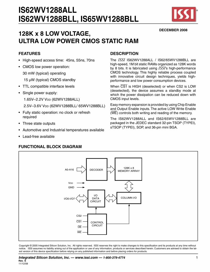
450-mil Plastic SOPPackage Code: Q (32-pin)
D
SEATING PLANE
Be C
1
N
E1
A1
A
E
L α
S
MILLIMETERS INCHES
Symbol Min. Max. Min. Max.No. Leads 32
A — 3.00 — 0.118A1 0.10 — 0.004 —B 0.36 0.51 0.014 0.020C 0.15 0.30 0.006 0.012D 20.14 20.75 0.793 0.817E 13.87 14.38 0.546 0.566
E1 11.18 11.43 0.440 0.450e 1.27 BSC 0.050 BSCL 0.58 0.99 0.023 0.039α 0° 10° 0° 10°S — 0.86 — 0.034
Notes:1. Controlling dimension: inches, unless
otherwise specified.2. BSC = Basic lead spacing between centers.3. Dimensions D and E1 do not include mold
flash protrusions and should be measuredfrom the bottom of the package.
4. Formed leads shall be planar with respect toone another within 0.004 inches at theseating plane.
Integrated Silicon Solution, Inc.
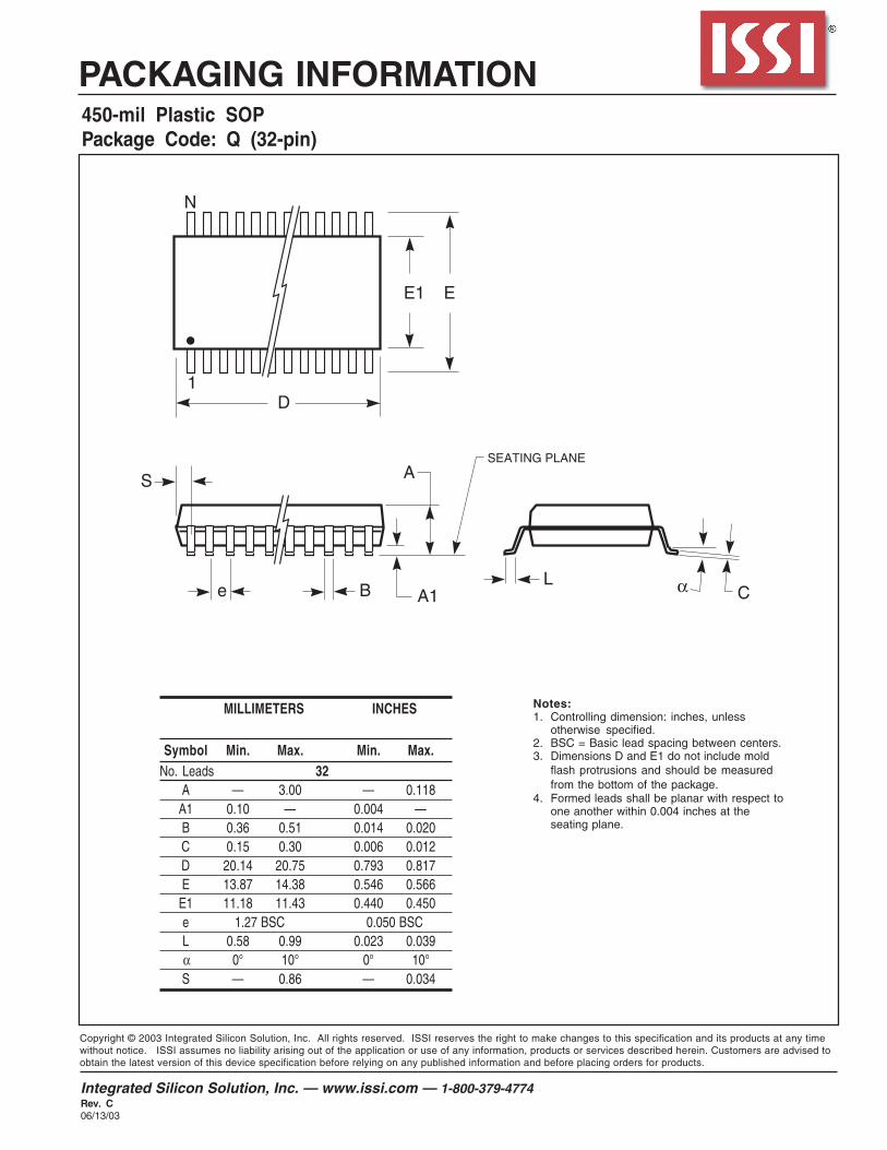
PACKAGING INFORMATIONPlastic STSOP - 32 pinsPackage Code: H (Type I)
Notes:1. Controlling dimension: millimeters, unless otherwise
specified.2. BSC = Basic lead spacing between centers.3. Dimensions D1 and E do not include mold flash protru-
sions and should be measured from the bottom of the package.4. Formed leads shall be planar with respect to one another
within 0.004 inches at the seating plane.
Plastic STSOP (H - Type I)Millimeters Inches
Symbol Min Max Min MaxRef. Std.
N 32A — 1.25 — 0.049
A1 0.05 — 0.002 —A2 0.95 1.05 0.037 0.041b 0.17 0.23 0.007 0.009C 0.14 0.16 0.0055 0.0063D 13.20 13.60 0.520 0.535
D1 11.70 11.90 0.461 0.469E 7.90 8.10 0.311 0.319e 0.50 BSC 0.020 BSCL 0.30 0.70 0.012 0.028S 0.28 Typ. 0.011 Typ.α 0° 5° 0° 5°
PK13197H32 Rev. B 04/21/03
D1 SEATING PLANE
C
D
1 N
e
S
b
A1A
A2
E
L α

Integrated Silicon Solution, Inc. — www.issi.com — 1-800-379-4774Rev. E01/15/03
Copyright © 2003 Integrated Silicon Solution, Inc. All rights reserved. ISSI reserves the right to make changes to this specification and its products at any timewithout notice. ISSI assumes no liability arising out of the application or use of any information, products or services described herein. Customers are advised toobtain the latest version of this device specification before relying on any published information and before placing orders for products.
PACKAGING INFORMATIONMini Ball Grid ArrayPackage Code: B (36-pin)
Notes:1. Controlling dimensions are in millimeters.
mBGA - 6mm x 8mm
MILLIMETERS INCHES
Sym. Min. Typ. Max. Min. Typ. Max.
N0.Leads 36 36
A — — 1.20 — — 0.047A1 0.24 — 0.30 0.009 — 0.012A2 0.60 — — 0.024 — —D 7.90 8.00 8.10 0.311 0.315 0.319D1 5.25BSC 0.207BSCE 5.90 6.00 6.10 0.232 0.236 0.240E1 3.75BSC 0.148BSC
e 0.75BSC 0.030BSC
b 0.30 0.35 0.40 0.012 0.014 0.016
mBGA - 8mm x 10mm
MILLIMETER INCHES
Sym. Min. Typ. Max. Min. Typ. Max.
N0.Leads 36 36
A — — 1.20 — — 0.047A1 0.24 — 0.30 0.009 — 0.012A2 0.60 — — 0.024 — —D 9.90 10.00 10.10 0.390 0.394 0.398D1 5.25BSC .207BSCE 7.90 8.00 8.10 0.311 0.315 0.319E1 3.75BSC 0.148BSC
e 0.75BSC 0.030BSC
b 0.30 0.35 0.40 0.012 0.014 0.016
SEATING PLANE
A
A1
A2
A
B
C
D
E
F
G
H
e
e
D1
E1E
D
φ b (36x)
Top View Bottom View
6 5 4 3 2 11 2 3 4 5 6
A
B
C
D
E
F
G
H

PACKAGING INFORMATION
Integrated Silicon Solution, Inc. — www.issi.com — 1-800-379-4774Rev. C06/13/03
Copyright © 2003 Integrated Silicon Solution, Inc. All rights reserved. ISSI reserves the right to make changes to this specification and its products at any timewithout notice. ISSI assumes no liability arising out of the application or use of any information, products or services described herein. Customers are advised toobtain the latest version of this device specification before relying on any published information and before placing orders for products.
Plastic TSOP-Type IPackage Code: T (32-pin)
D
SEATING PLANE
Be C
1
N
E
A1
AS
H
L α
Notes:1. Controlling dimension: millimeters, unless
otherwise specified.2. BSC = Basic lead spacing between centers.3. Dimensions D and E do not include mold
flash protrusions and should be measuredfrom the bottom of the package.
4. Formed leads shall be planar with respectto one another within 0.004 inches at theseating plane.
MILLIMETERS INCHES
Symbol Min. Max. Min. Max.No. Leads 32
A — 1.20 — 0.047A1 0.05 0.25 0.002 0.010B 0.17 0.23 0.007 0.009C 0.12 0.17 0.005 0.007D 7.90 8.10 0.311 0.319E 18.30 18.50 0.720 0.728H 19.80 20.20 0.780 0.795e 0.50 BSC 0.020 BSCL 0.40 0.60 0.016 0.024α 0° 8° 0° 8°S 0.25 REF 0.010 REF