Embed Size (px)
Citation preview
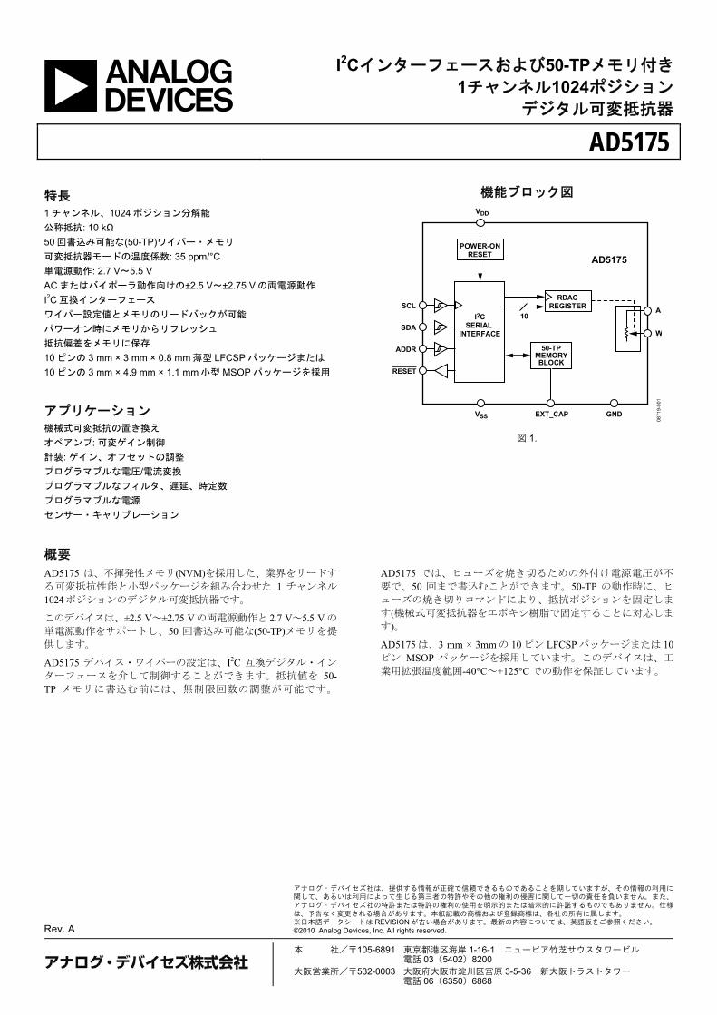
I2Cインターフェースおよび50-TPメモリ付き
1チャンネル1024ポジション デジタル可変抵抗器
AD5175
Rev. A
アナログ・デバイセズ社は、提供する情報が正確で信頼できるものであることを期していますが、その情報の利用に関して、あるいは利用によって生じる第三者の特許やその他の権利の侵害に関して一切の責任を負いません。また、アナログ・デバイセズ社の特許または特許の権利の使用を明示的または暗示的に許諾するものでもありません。仕様は、予告なく変更される場合があります。本紙記載の商標および登録商標は、各社の所有に属します。 ※日本語データシートは REVISION が古い場合があります。最新の内容については、英語版をご参照ください。 ©2010 Analog Devices, Inc. All rights reserved.
本 社/105-6891 東京都港区海岸 1-16-1 ニューピア竹芝サウスタワービル 電話 03(5402)8200
大阪営業所/532-0003 大阪府大阪市淀川区宮原 3-5-36 新大阪トラストタワー 電話 06(6350)6868
特長 1 チャンネル、1024 ポジション分解能
公称抵抗: 10 kΩ
50 回書込み可能な(50-TP)ワイパー・メモリ
可変抵抗器モードの温度係数: 35 ppm/°C
単電源動作: 2.7 V~5.5 V
AC またはバイポーラ動作向けの±2.5 V~±2.75 V の両電源動作
I2C 互換インターフェース
ワイパー設定値とメモリのリードバックが可能
パワーオン時にメモリからリフレッシュ
抵抗偏差をメモリに保存
10 ピンの 3 mm × 3 mm × 0.8 mm 薄型 LFCSP パッケージまたは
10 ピンの 3 mm × 4.9 mm × 1.1 mm 小型 MSOP パッケージを採用
アプリケーション 機械式可変抵抗の置き換え
オペアンプ: 可変ゲイン制御
計装: ゲイン、オフセットの調整
プログラマブルな電圧/電流変換
プログラマブルなフィルタ、遅延、時定数
プログラマブルな電源
センサー・キャリブレーション
機能ブロック図
10
VDD
A
W
AD5175
SCL
ADDR
SDA
I2CSERIAL
INTERFACE
POWER-ONRESET
RDACREGISTER
50-TPMEMORYBLOCK
RESET
VSS EXT_CAP GND
0871
9-0
01
図 1.
概要 AD5175 は、不揮発性メモリ(NVM)を採用した、業界をリードす
る可変抵抗性能と小型パッケージを組み合わせた 1 チャンネル
1024ポジションのデジタル可変抵抗器です。
このデバイスは、±2.5 V~±2.75 Vの両電源動作と 2.7 V~5.5 V の
単電源動作をサポートし、50 回書込み可能な(50-TP)メモリを提
供します。
AD5175 デバイス・ワイパーの設定は、I2C 互換デジタル・イン
ターフェースを介して制御することができます。抵抗値を 50-TP メモリに書込む前には、無制限回数の調整が可能です。
AD5175 では、ヒューズを焼き切るための外付け電源電圧が不
要で、50 回まで書込むことができます。50-TP の動作時に、ヒ
ューズの焼き切りコマンドにより、抵抗ポジションを固定しま
す(機械式可変抵抗器をエポキシ樹脂で固定することに対応しま
す)。
AD5175 は、3 mm × 3mm の 10 ピン LFCSP パッケージまたは 10ピン MSOP パッケージを採用しています。このデバイスは、工
業用拡張温度範囲-40°C~+125°C での動作を保証しています。

AD5235
Rev. A - 2/20 -
目次 特長......................................................................................................1 アプリケーション ..............................................................................1 機能ブロック図 ..................................................................................1 概要......................................................................................................1 改訂履歴 ..............................................................................................2 仕様......................................................................................................3
電気的特性......................................................................................3
インターフェース・タイミング仕様 ..........................................4
絶対最大定格 ......................................................................................6 熱抵抗..............................................................................................6
ESDの注意 ......................................................................................6
ピン配置およびピン機能説明 ..........................................................7 代表的な性能特性 ..............................................................................8 テスト回路 ........................................................................................11 動作原理 ............................................................................................12
シリアル・データ・インターフェース ....................................12
シフトレジスタ............................................................................ 12
書込み動作.................................................................................... 13
読出し動作.................................................................................... 15
RDACレジスタ............................................................................. 16
50-TPメモリ・ブロック .............................................................. 16
書込み保護機能............................................................................ 16
50-TPメモリ書込み―アクノリッジ・ポーリング................... 18
リセット ....................................................................................... 18
シャットダウン・モード ............................................................ 18
RDACアーキテクチャ................................................................. 18
可変抵抗のプログラミング ........................................................ 18
EXT_CAPコンデンサ .................................................................. 19
ピン電圧の動作範囲.................................................................... 19
パワーアップ・シーケンス ........................................................ 19
外形寸法............................................................................................ 20 オーダー・ガイド........................................................................ 20
改訂履歴 7/10—Rev. 0 to Rev. A
Changes to Ordering Guide ................................................................20
3/10—Revision 0: Initial Version
AD5175
Rev. A - 3/20 -
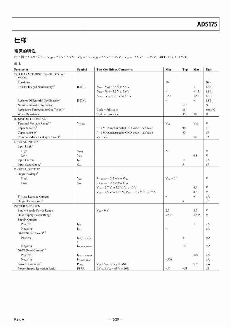
仕様
電気的特性 特に指定がない限り、VDD = 2.7 V~5.5 V、VSS = 0 V; VDD = 2.5 V~2.75 V、VSS = −2.5 V~−2.75 V; −40°C < TA < +125°C。
表 1.
Parameter Symbol Test Conditions/Comments Min Typ1 Max Unit
DC CHARACTERISTICS—RHEOSTAT MODE
Resolution 10 Bits
Resistor Integral Nonlinearity2, 3 R-INL |VDD − VSS| = 3.6 V to 5.5 V −1 +1 LSB
|VDD − VSS| = 3.3 V to 3.6 V −1 +1.5 LSB
|VDD − VSS| = 2.7 V to 3.3 V −2.5 +2.5 LSB
Resistor Differential Nonlinearity2 R-DNL −1 +1 LSB
Nominal Resistor Tolerance ±15 %
Resistance Temperature Coefficient4, 5 Code = full scale 35 ppm/°C
Wiper Resistance Code = zero scale 35 70 Ω
RESISTOR TERMINALS
Terminal Voltage Range4, 6 VTERM VSS VDD V
Capacitance A4 f = 1 MHz, measured to GND, code = half scale 90 pF
Capacitance W4 f = 1 MHz, measured to GND, code = half scale 40 pF
Common-Mode Leakage Current4 VA = VW 50 nA
DIGITAL INPUTS
Input Logic4
High VINH 2.0 V
Low VINL 0.8 V
Input Current IIN ±1 µA
Input Capacitance4 CIN 5 pF
DIGITAL OUTPUT
Output Voltage4
High VOH RPULL_UP = 2.2 kΩ to VDD VDD − 0.1 V
Low VOL RPULL_UP = 2.2 kΩ to VDD
VDD = 2.7 V to 5.5 V, VSS = 0 V 0.4 V
VDD = 2.5 V to 2.75 V, VSS = −2.5 V to −2.75 V 0.6 V
Tristate Leakage Current −1 +1 µA
Output Capacitance4 5 pF
POWER SUPPLIES
Single-Supply Power Range VSS = 0 V 2.7 5.5 V
Dual-Supply Power Range ±2.5 ±2.75 V
Supply Current
Positive IDD 1 µA
Negative ISS −1 µA
50-TP Store Current4, 7
Positive IDD_OTP_STOR
E 4 mA
Negative ISS_OTP_STORE −4 mA
50-TP Read Current4, 8
Positive IDD_OTP_READ 500 µA
Negative ISS_OTP_READ −500 µA
Power Dissipation9 PDISS VIH = VDD or VIL = GND 5.5 µW
Power Supply Rejection Ratio4 PSRR ΔVDD/ΔVSS = ±5 V ± 10% −50 −55 dB

AD5175
Rev. A - 4/20 -
Parameter Symbol Test Conditions/Comments Min Typ1 Max Unit
DYNAMIC CHARACTERISTICS4, 10
Bandwidth −3 dB, RAW = 5 kΩ, Terminal W, see Figure 23 700 kHz
Total Harmonic Distortion VA = 1 V rms, f = 1 kHz, RAW = 5 kΩ −90 dB
Resistor Noise Density RWB = 5 kΩ, TA = 25°C, f = 10 kHz 13 nV/√Hz 1 Typ 値は、25°C、VDD = 5 V、VSS = 0 V での平均測定値を表わします。 2 抵抗ポジション非直線性誤差 R-INL は、最大抵抗ワイパー・ポジションと最小抵抗ワイパー・ポジションとの間で測定された理論値からの差を表します。R-DNL は、
連続タップ・ポジション間での理論値からの相対的ステップ変化を表します。 3 各コードでの最大電流は、IAW = (VDD − 1)/RAWにより決定されます。 4 設計上保証しますが、出荷テストは行いません。 5 詳細については、図 8 を参照してください。 6 抵抗ピン Aと Wの極性は相互間で制約されません。両電源動作では、グラウンドを基準としたバイポーラ信号の調整が可能です。 7 動作電流とは異なります。ヒューズ書込みの電源電流は約 55 ms 間継続。 8 動作電流とは異なります。ヒューズ読出しの電源電流は約 500 ns 間継続。 9 PDISS は (IDD × VDD) + (ISS × VSS)で計算されます。 10 すべての動特性では、VDD = +2.5 Vかつ VSS = -2.5 V を使用。
インターフェース・タイミング仕様 特に指定のない限り、VDD = 2.7~5.5 V;すべての仕様は TMIN~TMAXで規定。
表 2.
Limit at TMIN, TMAX
Parameter Conditions1 Min Max Unit Description
fSCL2 Standard mode 100 kHz Serial clock frequency
Fast mode 400 kHz Serial clock frequency
t1 Standard mode 4 µs tHIGH, SCL high time
Fast mode 0.6 µs tHIGH, SCL high time
t2 Standard mode 4.7 µs tLOW, SCL low time
Fast mode 1.3 µs tLOW, SCL low time
t3 Standard mode 250 ns tSU;DAT, data setup time
Fast mode 100 ns tSU;DAT, data setup time
t4 Standard mode 0 3.45 µs tHD;DAT, data hold time
Fast mode 0 0.9 µs tHD;DAT, data hold time
t5 Standard mode 4.7 µs tSU;STA, set-up time for a repeated start condition
Fast mode 0.6 µs tSU;STA, set-up time for a repeated start condition
t6 Standard mode 4 µs tHD;STA, hold time (repeated) start condition
Fast mode 0.6 µs tHD;STA, hold time (repeated) start condition
High speed mode 160 ns tHD;STA, hold time (repeated) start condition
t7 Standard mode 4.7 µs tBUF, bus free time between a stop and a start condition
Fast mode 1.3 µs tBUF, bus free time between a stop and a start condition
t8 Standard mode 4 µs tSU;STO, setup time for a stop condition
Fast mode 0.6 µs tSU;STO, setup time for a stop condition
t9 Standard mode 1000 ns tRDA, rise time of the SDA signal
Fast mode 300 ns tRDA, rise time of the SDA signal
t10 Standard mode 300 ns tFDA, fall time of the SDA signal
Fast mode 300 ns tFDA, fall time of the SDA signal
t11 Standard mode 1000 ns tRCL, rise time of the SCL signal
Fast mode 300 ns tRCL, rise time of the SCL signal
t11A Standard mode 1000 ns tRCL1, rise time of the SCL signal after a repeated start condition and after an acknowledge bit
Fast mode 300 ns tRCL1, rise time of the SCL signal after a repeated start condition and after an acknowledge bit
t12 Standard mode 300 ns tFCL, fall time of the SCL signal
Fast mode 300 ns tFCL, fall time of the SCL signal
t13 RESET pulse time 20 ns Minimum RESET low time
tSP3 Fast mode 0 50 ns Pulse width of the spike is suppressed
tEXEC4, 5 500 ns Command execute time
tRDAC_R-PERF 2 µs RDAC register write command execute time (R-Perf mode)
tRDAC_NORMAL 600 ns RDAC register write command execute time (normal mode)
tMEMORY_READ 6 µs Memory readback execute time
tMEMORY_PROGRAM 350 ms Memory program time

AD5175
Rev. A - 5/20 -
Limit at TMIN, TMAX
Parameter Conditions1 Min Max Unit Description
tRESET 600 µs Reset 50-TP restore time
tPOWER-UP6 2 ms Power-on 50-TP restore time
1 最大バス容量は 400 pFに制限されます。 2 SDA と SCL のタイミングは入力フィルタをイネーブルして測定。入力フィルタを切り離すと、転送レートが向上しますが、デバイスの EMC動作に悪影響がありま
す。 3 SCL と SDA に入力フィルタを使うと、高速モードで 50 ns 以下にノイズ・スパイクが抑圧されます。 4 RDAC レジスタ書き込み動作については tRDAC_R-PERFと tRDAC_NORMALを参照してください。 5 メモリ・コマンド動作については、tMEMORY_READと tMEMORY_PROGRAMを参照してください。 6 VDD − VSS = 2.5 V となった後の最大時間。
シフトレジスタとタイミング図
DATA BITS
DB9 (MSB) DB0 (LSB)
D7 D6 D5 D4 D3 D2 D1 D0
CONTROL BITS
C0 C1 C2 D9 D8 C3 0 0
087
19-0
03
図 2.シフトレジスタの値
RESET
t7
t6
t2
t4
t11 t12 t6
t5t10
t1
SCL
SDA
P S S P
t3
t8
t9
t13
087
19-0
02
図 3. 2 線式 I2C のタイミング図
AD5175
Rev. A - 6/20 -
絶対最大定格 特に指定のない限り、TA = 25°C。
表 3.
Parameter Rating
VDD to GND –0.3 V to +7.0 V
VSS to GND +0.3 V to −7.0 V
VDD to VSS 7 V
VA, VW to GND VSS − 0.3 V, VDD + 0.3 V
Digital Input and Output Voltage to GND −0.3 V to VDD + 0.3 V
EXT_CAP to VSS 7 V
IA, IW
Pulsed1
Frequency > 10 kHz ±6 mA/d2
Frequency ≤ 10 kHz ±6 mA/√d2
Continuous ±6 mA
Operating Temperature Range3 −40°C to +125°C
Maximum Junction Temperature (TJ Maximum)
150°C
Storage Temperature Range −65°C to +150°C
Reflow Soldering
Peak Temperature 260°C
Time at Peak Temperature 20 sec to 40 sec
Package Power Dissipation (TJ max − TA)/θJA 1 最大ピン電流は、スイッチの最大処理電流、パッケージ最大消費電力、A ピ
ン、Wピン内の任意の 2 ピン間の、設定された抵抗での最大入力電圧により
制約されます。 2 パルス・デューティ・ファクタ。 3 50-TPメモリの書き込みを含みます。
上記の絶対最大定格を超えるストレスを加えるとデバイスに恒
久的な損傷を与えることがあります。この規定はストレス定格
の規定のみを目的とするものであり、この仕様の動作のセクシ
ョンに記載する規定値以上でのデバイス動作を定めたものでは
ありません。デバイスを長時間絶対最大定格状態に置くとデバ
イスの信頼性に影響を与えます。
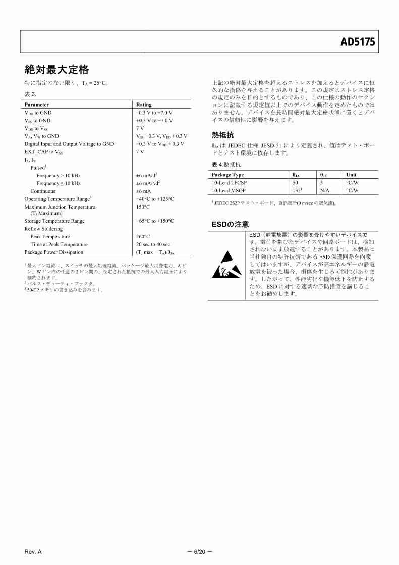
熱抵抗 θJA は JEDEC 仕様 JESD-51 により定義され、値はテスト・ボー
ドとテスト環境に依存します。
表 4.熱抵抗
Package Type θJA θJC Unit
10-Lead LFCSP 50 3 °C/W
10-Lead MSOP 1351 N/A °C/W 1 JEDEC 2S2Pテスト・ボード、自然空冷(0 m/sec の空気流)。
ESDの注意 ESD(静電放電)の影響を受けやすいデバイスで
す。電荷を帯びたデバイスや回路ボードは、検知
されないまま放電することがあります。本製品は
当社独自の特許技術である ESD 保護回路を内蔵
してはいますが、デバイスが高エネルギーの静電
放電を被った場合、損傷を生じる可能性がありま
す。したがって、性能劣化や機能低下を防止する
ため、ESD に対する適切な予防措置を講じるこ
とをお勧めします。

AD5175
Rev. A - 7/20 -
ピン配置およびピン機能説明
VDD 11
VSS
22A
33W
44 RESET
10
9
8
SCL
7
5EXT_CAP
SDA
6 GND
AD5175
TOP VIEW(Not to Scale)
ADDR
0871
9-0
04
*LEAVE FLOATING OR CONNECTED TO VSS.
ADDRVDD 1
VSS
2A
3W
4 RESET
10
9
8
SCL
7
5EXT_CAP
SDA
6 GND
AD5175
(EXPOSEDPAD)*
0871
9-1
03
図 4.MSOP ピン配置 図 5.LFCSP ピン配置
表 5.ピン機能の説明
ピン番号 記号 説明
1 VDD 正の電源。このピンは、0.1 µF のセラミック・コンデンサと 10 µF のコンデンサでデカップリングする必要がありま
す。
2 A RDAC の A ピン VSS ≤ VA ≤ VDD。
3 W RDAC のワイパー・ピン。VSS ≤ VW ≤ VDD。
4 VSS 負電源。単電源アプリケーションで 0 V へ接続してください。このピンは、0.1 µF のセラミック・コンデンサと 10 µF のコンデンサでデカップリングする必要があります。
5 EXT_CAP 外付けコンデンサ。1 µF のコンデンサを EXT_CAP と VSSの間に接続します。このコンデンサの定格電圧は 7 V 以上
である必要があります。
6 GND グラウンド・ピン、ロジック・グラウンド基準。
7 RESET ハードウェア・リセット・ピン。RDAC レジスタを 50-TP メモリ・レジスタ値でリセットします。最初に 50-TP ワイ
パー・メモリ・ロケーションが書込まれるまで、出荷時デフォルト値のミッド・スケールがロードされますRESETはアクティブ・ローです。使用しない場合は、RESETを VDDに接続してください。
8 SDA シリアル・データライン。このピンは、16 ビット入力レジスタにデータを入出力する SCL ラインと組み合わせて使
います。双方向のオープン・ドレイン・データ・ラインであるため、外付け抵抗で電源にプルアップする必要があり
ます。
9 SCL シリアル・クロック・ライン。このピンは、16 ビット入力レジスタにデータを入出力する SDA ラインと組み合わせ
て使います。
10 ADDR スリーステートのアドレス入力。7 ビット・スレーブ・アドレスの下位 2 ビット(ビットA1、ビットA0)を設定します(表 6 参照)。
EPAD エクスポー
ズド・パッ
ド
フローティングのままにするか、VSSへ接続してください。

AD5175
Rev. A - 8/20 -
代表的な性能特性 0.8
–0.6
–0.4
–0.2
0
0.2
0.4
0.6
0 128 256 384 512 640 768 896 1023
INL
(L
SB
)
CODE (Decimal)
+25°C–40°C+125°C
08
719
-01
4
図 6.ノーマル・モードでの R-INL 対コード対温度
0.4
–0.3
–0.2
–0.1
0
0.1
0.2
0.3
0 128 256 384 512 640 768 896 1023
DN
L (
LS
B)
CODE (Decimal)
+25°C–40°C+125°C
08
719
-01
5
図 7.コード対ノーマル・モードでの R-DNL 対温度
700
600
500
400
300
200
100
00 128 256 384 512 640 768 896 1023
RH
EO
ST
AT
MO
DE
TE
MP
CO
(p
pm
/°C
)
CODE (Decimal)
VDD/VSS = 5V/0V
08
71
9-0
19
図 8.コード対温度係数 ΔRWA/ΔT
0.7
0.6
0.5
0.4
0.3
0.2
0.1
0
–0.10 0.5 1.0 1.5 2.0 2.5 3.0 3.5 4.0 4.5 5.0 5.5
CU
RR
EN
T (
mA
)
VOLTAGE (V)
087
19-0
38
VDD/VSS = 5V/0V
図 9.デジタル入力電圧対電源電流(IDD)
–500
–400
–300
–200
–100
0
100
200
300
400
500C
UR
RE
NT
(n
A)
TEMPERATURE (°C)
–40 –30 –20 –10 0 20 30 40 50 60 70 80 90 100 11010
IDD = 5V
ISS = 5V
IDD = 3V
ISS = 3V
087
19-0
18
図 10.電源電流(IDD、ISS)の温度特性
7
0
1
2
3
4
5
6
0 1023850765 935680510 595340 425170 25585
TH
EO
RE
TIC
AL
l WA
_MA
X (
mA
)
CODE (Decimal) 0871
9-0
28
VDD/VSS = 5V/0V
図 11.コード対理論最大電流

AD5175
Rev. A - 9/20 -
087
19-0
31
VDD/VSS = 5V/0V–50
–45
–35
–40
–30
–25
–20
–15
–10
–5
0
1 10M1M100k10k1k10010
GA
IN (
dB
)
FREQUENCY (Hz)
0x040
0x020
0x010
0x008
0x0040x002
0x001
0x200
0x100
0x080
図 12.帯域幅対周波数対コード
TH
D +
N (
dB
)
0871
9-03
9
0
–120
–100
–80
–60
–40
–20
10 100 1k 10k 100k
FREQUENCY (Hz)
1M
VDD/VSS = ±2.5VCODE = HALF SCALEfIN = 1V rmsNOISE BW = 22kHz
図 13.THD + N の周波数特性
087
19-0
26
0
–100
–80
–60
–40
–20
0.001 0.01 0.1 1
TH
D +
N (
dB
)
AMPLITUDE (V rms)
10kΩ
VDD/VSS = ±2.5VCODE = HALF SCALEfIN = 1kHzNOISE BW = 22kHz
図 14.振幅対 THD + N
–20
–25
–30
–35
–40
–45
–50
–55
–6010 100 1M100k10k1k
PS
RR
(d
B)
FREQUENCY (Hz)
VDD/VSS = 5V/0VCODE = HALF SCALE
08
71
9-0
24
図 15.PSRR の周波数特性
4
5
6
7
8
VO
LT
AG
E (
V)
TIME (Seconds)
0.07 0.09 0.11 0.13 0.15 0.17
087
19-0
29
図 16.ヒューズ書込み時の VEXT_CAP波形
20
–70
–60
–50
–40
–30
–20
–10
0
10
–2 420
GL
ITC
H A
MP
LIT
UD
E (
mV
)
TIME (µs) 0871
9-10
2
VDD/VSS = ±2.5VIAW = 200µA
図 17.最大グリッチ・エネルギー

AD5175
Rev. A - 10/20 -
1.0
–1.5
–1.0
–0.5
0
0.5
–10 6050403020100
VO
LT
AG
E (
mV
)
TIME (µs) 0871
9-10
0
VDD/VSS = ±2.5VIAW = 200µA
図 18.デジタル・フィードスルー
0.006
–0.002
–0.001
0
0.001
0.002
0.003
0.004
0.005
0 1000900800700600500400300200100
ΔR
AW
RE
SIS
TA
NC
E (
%)
OPERATION AT 150°C (Hours) 0871
9-10
1
VDD/VSS = 5V/0VIAW = 10µACODE = HALF SCALE
図 19.バーンインにより加速した長時間ドリフト

AD5175
Rev. A - 11/20 -
テスト回路 図 20 ~図 24 に、仕様のセクションで使用したテスト条件を示します。
VMS
IW
A
W
DUT
087
19-0
33
図 20.抵抗ポジション非直線性誤差 (可変抵抗器動作; R-INL、R-DNL)
RWA =VMSIW
RW =RWA
2
A
W
IWDUT
VMS
CODE = 0x00
087
19-0
34
図 21.ワイパー抵抗
VDDIW
VMS
A
WV+
ΔVMS%ΔVDD%
VMSVDD
V+ = VDD ±10%
PSRR (dB) = 20 log
PSS (%/%) =
087
19-0
35
図 22.電源除去比(PSS、PSRR)
VMS
A
W
DUT
V
1GΩ
0871
9-0
36
図 23.ゲインの周波数特性
ICM
DUT
W
A
NC = NO CONNECT
GND
+2.75V
NC
+2.75V –2.75V
–2.75V
GND
GND
0871
9-03
7
図 24.コモン・リーク電流

AD5175
Rev. A - 12/20 -
動作原理 AD5175 は、VSS < VTERM < VDDのピン電圧範囲内のアナログ信号
に対して真の可変抵抗として動作するようにデザインされてい
ます。RDAC レジスタ値により抵抗ワイパー・ポジションが決
定されます。RDAC レジスタはスクラッチパッド・レジスタの
ように動作するため、抵抗設定値の変更回数には制限がありま
せん。RDAC レジスタには、I2C インターフェースを使って任意
のポジションを設定することができます。目的のワイパー・ポ
ジションが見つかった後に、この値を 50-TP メモリ・レジスタ
に保存することができます。それ以後、ワイパー・ポジション
は、後続パワーアップで常にそのポジションに回復されます。
50-TP データの保存には約 350ms 要し、この間 AD5175 がロッ
クされて、新しいコマンドをアクノリッジしないため、値の変
更が防止されます。アクノリッジ・ビットをポーリングして、
ヒューズ・プログラム・コマンドの完了を確認することができ
ます。
シリアル・データ・インターフェース AD5175 は、2 線式I2C互換シリアル・インターフェースを内蔵
しています。このインターフェースは、マスター・デバイスか
ら制御されるスレーブ・デバイスとしてI2Cバスに接続すること
ができます。書込みシーケンスのタイミング図については、図
3 を参照してください。
AD5175 は、標準(100 kHz)と高速(400 kHz)のデータ転送モード
をサポートしています。10 ビット・アドレシングとジェネラ
ル・コール・アドレシングはサポートされていません。
AD5175 は 7 ビットのスレーブ・アドレスを持っています。上位
5 ビットは 01011 で、下位 2 ビットはADDRピンの状態で指定さ
れます。 ADDRをハード・ワイヤー接続で変更する機能を使う
と、表 6 に示すように、1 つのバスにこれらのデバイスを最大 3個接続することができます。
2 線式シリアル・バス・プロトコルは、次のように動作します。
すなわち、マスターがスタート条件を設定してデータ転送を開
始させます。このスタート条件は、SCL がハイ・レベルの間に、
SDA ライン上でハイ・レベルからロー・レベルへの変化が起き
たときに発生します。次のバイトはアドレス・バイトであり、7ビットのスレーブ・アドレスと R/Wビットから構成されていま
す。送信されたアドレスに該当するスレーブ・デバイスは 9 番
目のクロック・パルスで、SDA ラインをロー・レベルにして応
答します(これはアクノリッジ・ビットと呼ばれます)。選択さ
れたデバイスがシフトレジスタに読み書きするデータを待つ間、
バス上の他の全デバイスはアイドル状態を維持します。
データは、9 個のクロック・パルスで 8 ビットのデータとそれ
に続くアクノリッジ・ビットの順にシリアル・バス上を伝送し
ます。SDA ラインは SCL のロー・レベル区間で変化して、SCLのハイ・レベル区間で安定に維持されている必要があります。
全データビットの読出しまたは書込みが終了すると、ストップ
条件が設定されます。書込みモードでは、マスターが 10 番目の
クロック・パルスで SDA ラインをハイ・レベルにプルアップし
て、ストップ状態を設定します。読出しモードでは、マスター
は 9 番目のクロック・パルスでアクノリッジを発行しません
(SDA ラインがハイ・レベルを維持)。この後、マスターは SDAラインをロー・レベルにして、10 番目のクロック・パルスがハ
イ・レベルになるときストップ条件を設定します。
シフトレジスタ AD5175 のシフトレジスタは、図 2 に示すように 16 ビット幅で
す。16 ビット・ワードは、未使用の 2 ビット(0 に設定)、それに
続く 4 ビットのコントロール・ビットと 10 ビットのRDACデー
タビットから構成されています。データはMSB(ビットD9)ファ
ーストでロードされます。4 ビットのコントロール・ビットは、
ソフトウェア・コマンドの機能を指定します(表 7 参照)。図 25 に、代表的な書込みシーケンスのタイミング図を示します。
コマンド・ビット(Cx)が、デジタル・ポテンショメータと内部
50-TP メモリの動作を制御します。データビット(Dx)は、デコー
ドされたレジスタにロードされる値です。
表 6.デバイス・アドレスの指定
ADDR Pin A1 A0 7-Bit I2C Device Address
GND 1 1 0101111
VDD 0 0 0101100
NC (No Connection)1 1 0 0101110 1 バイポーラ・モードでは使用できません。 VSS < 0 V。

AD5175
Rev. A - 13/20 -
書込み動作 RDAC レジスタまたはコントロール・レジスタに対してデータ
を書込むことができます。AD5175 へ書込みを行うときは、ま
ずスタート・コマンドを送信し、続いてアドレス・バイト(R/W = 0)を送信します。その後に AD5175 は SDA をロー・レベルに
して、データ受信の準備ができたことを通知します。
次に、2 バイトのデータ(上位バイトに続いて下位バイト)がRDACに書込まれます。これらのデータバイトはAD5175 により
アクノリッジされます。この後に、ストップ条件が続きます。
AD5175 に対する書込み動作を図 25 に示します。
繰り返し書込み機能は、デバイスに対するアドレシング指定を
1 回行うだけで、デバイスを複数回更新する柔軟性を提供しま
す(図 26 参照)。
SCL
SDA
START BYMASTER
ACK. BYAD5175
FRAME 1SERIAL BUS ADDRESS BYTE
FRAME 2MOST SIGNIFICANT DATA BYTE
FRAME 3LEAST SIGNIFICANT DATA BYTE
SCL (CONTINUED)
SDA (CONTINUED)
ACK. BYAD5175
ACK. BYAD5175
STOP BYMASTER
0
1 9
19 9
91
1 0 1 1 A1 A0 0 0 C3 C2 C1 C0 D9 D8
D7 D6 D5 D4 D3 D2 D1 D0
R/W
087
19-0
05
図 25.書込みコマンド

AD5175
Rev. A - 14/20 -
SCL
SDA 0
1 9
19 9
91
1 0 1 1 A1 A0 R/W 0 0 C3 C2 C1 C0 D9 D8
D7 D6 D5 D4 D3 D2 D1 D0
SCL (CONTINUED)
SDA (CONTINUED)
SCL (CONTINUED)
SDA (CONTINUED)
SCL (CONTINUED)
SDA (CONTINUED)
19 9
D7 D6 D5 D4 D3 D2 D1 D0
19 9
0 0 C3 C2 C1 C0 D9 D8
FRAME 4MOST SIGNIFICANT DATA BYTE
FRAME 5LEAST SIGNIFICANT DATA BYTE
START BYMASTER
ACK. BYAD5175
ACK. BYAD5175
ACK. BYAD5175
ACK. BYAD5175
ACK. BYAD5175
STOP BYMASTER
FRAME 1SERIAL BUS ADDRESS BYTE
FRAME 2MOST SIGNIFICANT DATA BYTE
FRAME 3LEAST SIGNIFICANT DATA BYTE
0871
9-0
06
図 26.複数回書込み
AD5175
Rev. A - 15/20 -
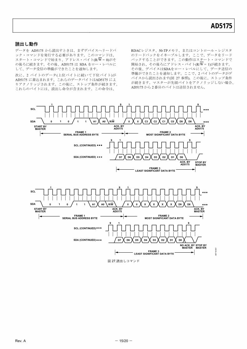
読出し動作 データを AD5175 から読出すときは、まずデバイスへリードバ
ック・コマンドを発行する必要があります。このコマンドは、
スタート・コマンドで始まり、アドレス・バイト(R/W = 0)がそ
の後ろに続きます。その後、AD5175 は SDA をロー・レベルに
して、データ受信の準備ができたことを通知します。
次に、2 バイトのデータ(上位バイトに続いて下位バイト)がAD5175 に書込まれます。これらのデータバイトはAD5175 によ
りアクノリッジされます。この後に、ストップ条件が続きます。
これらのバイトには、読出し命令が含まれます。この命令は、
RDACレジスタ、50-TPメモリ、またはコントロール・レジスタ
のリードバックをイネーブルします。ここで、データをリード
バックすることができます。この動作はスタート・コマンドで
開始され、その後ろにアドレス・バイト(R/W = 1)が続きます。
その後、デバイスはSDAをロー・レベルにして、データ送信の
準備ができたことを通知します。ここで、2 バイトのデータがデ
バイスから読出されます(図 27 参照)。この後に、ストップ条件
が続きます。マスターが先頭バイトをアクノリッジしない場合、
AD5175 から 2 番目のバイトは送信されません。
0
1 9
19 9
91
1 0 1 1 A1 A0 R/W 0 0 C3 C2 C1 C0 D9 D8
D7 D6 D5 D4 D3 D2 D1 D0
0
1 9
19 9
91
1 0 1 1 A1 A0 R/W 0 0 X X X X D9 D8
D7 D6 D5 D4 D3 D2 D1 D0
ACK. BYAD5175
ACK. BYAD5175
ACK. BYAD5175
ACK. BYAD5175
ACK. BYMASTER
NO ACK. BYMASTER
SCL
SDA
SCL (CONTINUED)
SDA (CONTINUED)
SCL (CONTINUED)
SDA (CONTINUED)
START BYMASTER
SCL
SDA
START BYMASTER
STOP BYMASTER
STOP BYMASTER
FRAME 1SERIAL BUS ADDRESS BYTE
FRAME 1SERIAL BUS ADDRESS BYTE
FRAME 2MOST SIGNIFICANT DATA BYTE
FRAME 2MOST SIGNIFICANT DATA BYTE
FRAME 3LEAST SIGNIFICANT DATA BYTE
FRAME 3LEAST SIGNIFICANT DATA BYTE 08
719-
007
図 27.読出しコマンド

AD5175
Rev. A - 16/20 -
RDACレジスタ RDAC レジスタは、デジタル可変抵抗器のワイパー・ポジショ
ンを直接制御します。例えば、RDAC レジスタに全ビット 0 を
ロードすると、ワイパーは可変抵抗の A ピンに接続されます。
I2C インターフェースを使って RDAC レジスタの書込みと読出
しを行うことができます。RDAC レジスタは標準のロジック・
レジスタであるため、許容変更回数には制限がありません。
50-TPメモリ・ブロック AD5175は、50-TPのプログラマブルなメモリ・レジスタのアレ
イを内蔵しています。このメモリ・レジスタを使うと、ワイパ
ー・ポジションを最大50回分書込むことができます。表11にメ
モリ・マップを示します。表7に示すコマンド3は、RDACレジ
スタ値をメモリへ書込みます。書込む先頭アドレスは、ロケー
ション0x01に配置されています(表11参照)。後続の各書込みご
とに、AD5175はメモリがフルになるまで50-TPメモリ・アドレ
スをインクリメントします。50-TPへのデータの書込みでは、55 ms間に約4 mAを消費し、完了までに約350 msを要します。この
間、シフトレジスタがロックされて、変更されないように保護
されます。表10に示すコントロール・レジスタのビットC2をポ
ーリングして、ヒューズ・プログラム・コマンドが正常に完了
したことを確認することができます。50-TPメモリの書込み時は、
電源電圧の変化は許されませんが、EXT_CAPピンに1 µFのコン
デンサは必要です(図29参照)。
50-TPをアクティブにする前は、パワーアップ時にAD5175はミッ
ドスケールに設定されます。コマンド5を使って、I2Cインター
フェースから任意の50-TPメモリ・レジスタ値をリードバックす
ることができます(表7)。データバイトの下位6ビット(D0~D5)により、リードバック対象のメモリ・ロケーションが選択され
ます。コマンド6を使うと、直前に書込まれたワイパー・メモ
リ・ロケーションのバイナリ符号化されたアドレスをリードバ
ックすることができます(表7)。この機能は、50-TPメモリ・ブ
ロックのスペア・メモリ・ステータスをモニタするときに使う
ことができます。
書込み保護機能 パワーアップ時に、RDACレジスタと 50-TPメモリ・レジスタに
対するシリアル・データ入力レジスタ書込みコマンドがディス
エーブルされます。コントロール・レジスタのRDAC書込み保
護ビットC1(表 9 と 表 10 参照)は、デフォルトで 0 に設定されま
す。これにより、ソフトウェア・コマンドに無関係にRDACレジ
スタ値の変更が禁止されます。ただし、ソフトウェア・リセッ
ト(コマンド 4)またはハードウェアのRESETピンを使って、
RDACレジスタを 50-TPメモリからリフレッシュすることはでき
ます。可変抵抗ワイパー・ポジションの書込み(RDACレジスタ
の書込み)をイネーブルときは、コントロール・レジスタの書込
み保護ビットC1 を先に設定する必要があります。これは、シリ
アル・データ入力レジスタにコマンド 7 をロードすることによ
り行われます(表 7)。50-TPメモリ・ブロック・ビットの書込み
をイネーブルするときは、コントロール・レジスタのC0 (デフ
ォルトで 0 に設定済み)を最初に 1 に設定する必要があります。
表 7.コマンド動作の真理値表
Command[DB13:DB10] Data[DB9:DB0]1 Command Number C3 C2 C1 C0 D9 D8 D7 D6 D5 D4 D3 D2 D1 D0 Operation
0 0 0 0 0 X X X X X X X X X X NOP: do nothing.
1 0 0 0 1 D9 D8 D7 D6 D5 D4 D3 D2 D1 D Write contents of serial register data to RDAC.
2 0 0 1 0 X X X X X X X X X X Read contents of RDAC wiper register.
3 0 0 1 1 X X X X X X X X X X Store wiper setting: store RDAC setting to 50-TP.
4 0 1 0 0 X X X X X X X X X X Software reset: refresh RDAC with the last 50-TP memory stored value.
52 0 1 0 1 X X X X D5 D4 D3 D2 D1 D0 Read contents of 50-TP from the SDO output in the next frame.
6 0 1 1 0 X X X X X X X X X X Read address of the last 50-TP programmed memory location.
73 0 1 1 1 X X X X X X X X D1 D0 Write contents of the serial register data to the control register.
8 1 0 0 0 X X X X X X X X X X Read contents of the control register.
9 1 0 0 1 X X X X X X X X X D0 Software shutdown.
D0 = 0; normal mode.
D0 = 1; shutdown mode. 1 X = don’t care. 2 50-TPメモリ・マップについては表 11 を参照してください。 3 詳細については、表 10 を参照してください。

AD5175
Rev. A - 17/20 -
表 8.RDAC と 50-TP メモリの書込みと読出し
DIN SDO1 Action
0x1C03 0xXXXX
Enable update of wiper position and 50-TP memory contents through digital interface.
0x0500 0x1C03 Write 0x100 to the RDAC register, wiper moves to ¼ full-scale position.
0x0800 0x0500 Prepare data read from RDAC register.
0x0C00 0x100 Stores RDAC register content into 50-TP memory. 16-bit word appears out of SDO, where the last 10-bits contain the contents of the RDAC Register 0x100.
0x1800 0x0C00 Prepare data read of the last programmed 50-TP memory monitor location.
0x0000 0xXX19 NOP Instruction 0 sends a 16-bit word out of SDO, where the six LSBs (that is, the last 6 bits) contain the binary address of the last programmed 50-TP memory location, for example, 0x19 (see Table 11).
0x1419 0x0000 Prepares data read from Memory Location 0x19.
0x2000 0x0100 Prepare data read from the control register. Sends a 16-bit word out of SDO, where the last 10-bits contain the contents of Memory Location 0x19.
0x0000 0xXXXX
NOP Instruction 0 sends a 16-bit word out of SDO, where the last four bits contain the contents of the control register. If Bit C2 = 1, fuse program command successful.
1 X = don’t care。
表 9.コントロール・レジスタのビット・マップ
DB9 DB8 DB7 DB6 DB5 DB4 DB3 DB2 DB1 DB0
0 0 0 0 0 0 C2 0 C1 C0
表 10.コントロール・レジスタの説明
Bit Name Description
C0 50-TP program enable
0 = 50-TP program disabled (default)
1 = enable device for 50-TP program
C1 RDAC register write protect
0 = wiper position frozen to value in OTP memory (default)1
1 = allow update of wiper position through a digital interface
C2 50-TP memory program success bit
0 = fuse program command unsuccessful (default)
1 = fuse program command successful 1 ワイパー・ポジションは 50-TP メモリに直前に書込んだ値に固定されます。50-TP メモリに書込みが行われない場合は、ワイパーはミッドスケールに固定されます。
表 11.メモリ・マップ
Data Byte[DB9:DB0]1
Command Number D9 D8 D7 D6 D5 D4 D3 D2 D1 D0 Register Contents
X X X 0 0 0 0 0 0 0 Reserved
X X X 0 0 0 0 0 0 1 1st programmed wiper location (0x01)
X X X 0 0 0 0 0 1 0 2nd programmed wiper location (0x02)
X X X 0 0 0 0 0 1 1 3rd programmed wiper location (0x03)
X X X 0 0 0 0 1 0 0 4th programmed wiper location (0x04)
… … … … … … … … … … …
X X X 0 0 0 1 0 1 0 10th programmed wiper location (0xA)
… … … … … … … … … … …
X X X 0 0 1 0 1 0 0 20th programmed wiper location (0x14)
… … … … … … … … … … …
X X X 0 0 1 1 1 1 0 30th programmed wiper location (0x1E)
… … … … … … … … … … …
X X X 0 1 0 1 0 0 0 40th programmed wiper location (0x28)
… … … … … … … … … … …
X X X 0 1 1 0 0 1 0 50th programmed wiper location (0x32)
… … … … … … … … … … …
X X X 0 1 1 1 0 0 1 MSB resistance tolerance (0x39)
5
X X X 0 1 1 1 0 1 0 LSB resistance tolerance (0x3A) 1 X = don’t care。

AD5175
Rev. A - 18/20 -
50-TPメモリ書込み―アクノリッジ・ポーリング 50-TP レジスタに対する各書込み動作の後に、内部書込みサイ
クルが開始されます。デバイスの I2C インターフェースはディ
スエーブルされます。内部書込みサイクルの終了と I2C インタ
ーフェースのイネーブルを確認するために、インターフェース
のポーリングを行うことができます。I2C インターフェースのポ
ーリングは、スタート条件を送信し、続いてスレーブ・アドレ
スと書込みビットを送信することにより実行することができま
す。I2C インターフェースがアクノリッジ(ACK)で応答してくる
場合、書込みサイクルが完了し、インターフェースは次の動作
が可能であることを意味します。その他の場合には、I2C インタ
ーフェースのポーリングが完了するまで繰り返すことができま
す。
リセット コマンド 4 を実行することによりソフトウェアからAD5175 をリ
セットすることもできます(表 7 参照)。あるいは、ハードウェ
アによりRESETピンにロー・レベル・パルスを入力することに
よりリセットすることもできます。リセット・コマンドにより、
直前に書込まれた 50-TPメモリ・ロケーションの値がRDACレジ
スタにロードされます。直前に書込まれた 50-TPメモリ・ロケ
ーションがない場合には、RDACレジスタにミッドスケールが
ロードされます。使用しない場合は、RESETをVDDに接続して
ください。
シャットダウン・モード AD5175 は、ソフトウェア・シャットダウン・コマンド(コマンド
9)を実行してLSBに 1 を設定することにより、シャットダウンす
ることができます(表 7 参照)。この機能によりRDACはゼロ消費
電力状態になり、ピンAはワイパー・ピンから切り離されます。
AD5175 がシャットダウン・モードにあるとき、表 7 の全コマン
ドを実行することができます。コマンド 9 を実行して、LSBを 0に設定するか、またはソフトウェア・リセットまたはハードウ
ェア・リセットを発行することにより、デバイスをシャットダ
ウン・モードから抜け出させることができます。
RDACアーキテクチャ 最適性能を実現するため、アナログ・デバイセズはすべてのデジ
タル・ポテンショメータに対してRDACセグメント化アーキテ
クチャの特許を取得しました。特に、AD5175 では 3 ステージ・
セグメント化を採用しています(図 28 参照)。AD5175 ワイパ
ー・スイッチは、トランスミッション・ゲートCMOS回路を採用
してデザインされています。
A
W
10-BITADDRESSDECODER
RL
RL RM
RM
RW
SW
RW
0871
9-00
8
図 28.簡略化した RDAC 回路
可変抵抗のプログラミング
可変抵抗器動作
ピン W とピン A の間の公称抵抗(RWA)は 10 kΩであり、ワイパ
ー・ピンからアクセスされるタップ・ポイント数は 1024 です。
RDAC ラッチ内の 10 ビット・データがデコードされて、1024通りのワイパー設定の内の 1 つを選択します。このため、W ピ
ンと A ピンとの間のデジタル的に設定する出力抵抗を決定する
一般式は次のようになります。
WAWA RDDR 1024
)( (1)
ここで、 D は、10 ビット RDAC レジスタにロードされるバイナリ・コー
ド・データの 10 進数表示。 RWAはピン間抵抗。
ゼロ・スケール状態では、有限な合計ワイパー抵抗が 120Ωとな
ります。デバイスが動作している設定に関らず、A ピン―Wピン
間と、Wピン―Bピン間の電流を最大連続電流±6 mAまたは 表 3に規定するパルス電流に制限するように注意する必要がありま
す。そうしないと、内部スイッチ・コンタクトの性能低下また
は破壊が生ずる恐れがあります。

AD5175
Rev. A - 19/20 -
実際のピン間抵抗の計算
抵抗偏差は工場出荷テスト時に内部メモリに保存されます。こ
のため、実際のピン間抵抗を計算することができ、これはキャ
リブレーション、偏差の一致、高精度アプリケーションで役立
ちます。
パーセント抵抗偏差は、固定小数点フォーマットにより 16 ビッ
ト符号付きバイナリで保存されています。符号ビット(0 =負お
よび 1 =正)と整数部分はアドレス 0x39 に配置されています(表11 参照)。アドレス 0x3Aには非整数部分が配置されています(表12 参照)。
すなわち、アドレス 0x39 からのデータ・リードバックが
0000001010 で、かつアドレス 0x3A からのデータが 0010110000 の
場合、ピン間抵抗は次のように計算されます。
メモリ・ロケーション 0x39 の場合
DB[9:8]: XX = don’t care DB[7]: 0 =負
DB[6:0]: 0001010 = 10
メモリ・ロケーション 0x3A の場合
DB[9:8]: XX = don’t care
DB[7:0]: 10110000 = 176 × 2−8 = 0.6875
したがって、偏差= −10.6875%で、RWA (1023)= 8.931 kΩ.
EXT_CAPコンデンサ パワーアップ時とAD5175 の動作中に、1 µFのコンデンサを
EXT_CAPピンとVSSとの間に接続する必要があります(図 29 参
照)。
AD5175
50-TPMEMORYBLOCK
EXT_CAPC1
1µF
VSS
VSS
087
19-0
09
図 29.EXT_CAP ハードウェアのセットアップ
ピン電圧の動作範囲 AD5175の正側VDD電源と負側VSS電源により、2端子デジタル抵
抗動作の動作範囲が決定されます。VDDまたはVSSを超えてピン
AとピンWに入力される電源信号は、内蔵の順方向バイアス・
ダイオードによりクランプされます(図30参照)。
VSS
VDD
A
W
087
19-1
09
図 30.VDDと VSSにより設定される最大ピン電圧
AD5175のグラウンド・ピンは、主にデジタル・グラウンド基準
として使われます。デジタル・グラウンド・バウンズを最小に
するため、AD5175のグラウンド・ピンはコモン・グラウンドか
ら離れた所で接続する必要があります。AD5175に対するデジタ
ル入力コントロール信号はデバイス・グラウンド・ピン(GND)を基準として、仕様のセクションに規定するロジック・レベル
を満たす必要があります。内蔵のレベル・シフト回路は、デジ
タル入力レベルに無関係に、3本のピンの同相モード電圧範囲を
VSSからVDDへ確実に拡張します。
パワーアップ・シーケンス ピンAとピンWでの電圧コンプライアンスを制限するダイオー
ドが内蔵されているため(図30)、ピンAとピンWに電圧を加える
前に先にVDD/VSSを加えることが重要です。そうしないと、ダイ
オードが順方向バイアスされて、意図せずにVDD/VSSに電源が接
続されてしまいます。最適なパワーアップ・シーケンスは、VSS、
GND、VDDデジタル入力の順、続いてVA、VWの順序です。電源
投入シーケンスVA、VW、デジタル入力の順は、VDD/VSS投入後
であれば、重要ではありません。
VDDが加わると直ちに、パワーオン・プリセットが起動されま
す。これにより先ずRDACがミッドスケールに設定され、次に
最後に書込まれた50-TP値がRDACレジスタに復元されます。
表 12.ピン間抵抗偏差の各バイト
Data Byte1
Memory Map Address DB9 DB8 DB7 DB6 DB5 DB4 DB3 DB2 DB1 DB0
0x39 X X Sign 26 25 24 23 22 21 20
0x3A X X 2−1 2−2 2−3 2−4 2−5 2−6 2−7 2−8 1X は don't care

AD5175
Rev. A - 20/20 -
外形寸法 2.482.382.23
0.500.400.30
1210
09-A
TOP VIEW
10
1
6
5
0.300.250.20
BOTTOM VIEW
PIN 1 INDEXAREA
SEATINGPLANE
0.800.750.70
1.741.641.49
0.20 REF
0.05 MAX0.02 NOM
0.50 BSC
EXPOSEDPAD
3.103.00 SQ2.90
PIN 1INDICATOR(R 0.15)
FOR PROPER CONNECTION OFTHE EXPOSED PAD, REFER TOTHE PIN CONFIGURATION ANDFUNCTION DESCRIPTIONSSECTION OF THIS DATA SHEET.
図 31.10 ピン・リードフレーム・チップ・スケール・パッケージ[LFCSP_WD] 3 mm × 3 mm ボディ、極薄、デュアル・リード(CP-10-9)
寸法: mm
COMPLIANT TO JEDEC STANDARDS MO-187-BA 0917
09-A
6°0°
0.700.550.40
5
10
1
6
0.50 BSC
0.300.15
1.10 MAX
3.103.002.90
COPLANARITY0.10
0.230.13
3.103.002.90
5.154.904.65
PIN 1IDENTIFIER
15° MAX0.950.850.75
0.150.05
図 32.10 ピン・ミニ・スモール・アウトライン・パッケージ[MSOP] (RM-10) 寸法: mm
オーダー・ガイド
Model1 RAB (kΩ) Resolution Temperature Range Package Description Package Option Branding
AD5175BRMZ-10 10 1,024 −40°C to +125°C 10-Lead MSOP RM-10 DDR
AD5175BRMZ-10-RL7 10 1,024 −40°C to +125°C 10-Lead MSOP RM-10 DDR
AD5175BCPZ-10-RL7 10 1,024 −40°C to +125°C 10-Lead LFCSP_WD CP-10-9 DEG 1 Z = RoHS 準拠製品。 I2C は、Philips Semiconductors 社(現在の NXP Semiconductors 社)が開発した通信プロトコルです。