Embed Size (px)
Citation preview

T021607_XC4VFX60
Synopsis V1.0 Heavy ion SEE test of Virtex4 FPGA XC4VFX60 from Xilinx
Christian Poivey1, Melanie Berg1, Scott Stansberry2, Mark Friendlich1, Hak Kim1,
Dave Petrick3, Ken LaBel3
1Muniz Engineering Inc. 2University of Southern California
3NASA-GSFC
Test Date(s): February 16-19, 2007 Report Date: June 28, 2007
I. Introduction
This study has been undertaken to determine the single event effect susceptibility of the Xilinx Virtex 4 Field Programmable Gate Array (FPGA) XC4VFX60. Device under test (DUT) was monitored for destructive and non destructive events induced by exposing it to a heavy ion beam at the Texas A&M Cyclotron Single Event Effects Test Facility. Test was performed in the frame of HST/RNS project.
II. Devices Tested
Device technology is 90 nm Copper CMOS. Device is packaged in a 1152 pin flip-chip fine pitch BGA package. Device cross-sections is shown in Figure 1. Max package thickness is 2.8mm. Lid (heat spreader) thickness is 0.65 +/- 0.05 mm. Die thickness is between 0.725 and 0.775 mm. Five samples were prepared for the tests. Lid was removed and die was thinned down to 100 µm. Then, test samples were mounted on daughter boards.
Figure 1: Device cross-section

T021607_XC4VFX60
The five test samples were coming from HST/RNS flight lots. Package marking of
test samples are: Xilinx Xilinx Virtex-4 Virtex4 XC4VFX60 XC4VFX60 FF1152DGQ0609 FF1152DGQ0609 DD1401594A DD1394545A 11I-ES1 11I-ES1
III. Test Facility
Facility: TEXAS A&M Cyclotron Single Event Effects Test Facility Beam: 25 MeV/u Flux: 10 to 1 x 10³ particles/cm2/s. Fluence: all tests were run to 1 x 10⁶ p/cm2 or until functional events occurred. Characteristics of ions used for these tests are shown in Table 1.
Table 1: Characteristics of ions used for the tests Ion Type Energy
(MeV) LET on target (MeVcm2/mg)
Range on target (µµµµm)
Ar 929 5.7 445 Kr 1858 20.6 284 Xe 2758 40.7 237
IV. Space Cube Application
Core of Space Cube is made of four Power PC (in two XC4VFX60 FPGA),
working in quadruple module redundancy to mitigate any SEE happening in the FPGAs. Voting is performed in a “radiation hardened” Aeroflex FPGA. FPGA configuration memory is scrubbed either with Xilinx self-scrubbing algorithms or an external scrubber running in Aeroflex FPGAs.
Power PCs do not work synchronously. External bus is 16 bits wide. Each Power PC uses 2Gx18 bits of external memory. Each Power PC has its own separate memory bank, but there is no separate memory bank for instruction and data. FPGA BRAM is used in the application as a boot loader. After the device is programmed, the Power PC uses the boot loader code stored in the BRAM to load in the operating system and applications from external flash memory to the SDRAM.
MGTs are not used in Space Cube application. All other I/Os are operated with a power supply voltage of 3.3V.
No PMCDs are currently used in the application, but multiple MCD are used. Power PC clock speed is 250 MHz. Clock speed for I/Os is 125 MHz.

T021607_XC4VFX60
V. Test Conditions and Error Modes
Test Temperature: ~60˚C (die)* Operating Frequency: 250 MHz for Power PC, 62 MHz for I/Os Power Supply Voltage: Vccint: 1.2V Vccaux: 2.5V
Vcco: 3.3V
* maximum junction temperature is 125˚C. Die temperature is given by DUT internal temperature sensing diode.
PARAMETERS OF INTEREST: Power supply currents, device functionality SEE Conditions: SEL, SEU, MEU, SET, SEFI
VI. Test Set-up
XC4VFX60 was tested with NASA-GSFC REAG (Radiation Effects and Analysis Group) high-speed digital tester (HSDT). HSDT is a reusable universal digital device tester based on Xilinx Virtex 2 Pro FPGA with input/output (I/O) operation speed up to 600 MHz.
High-speed tester is the main test board that interfaces with the DUT-specific
daughter card. The DUT on the daughter card is exercised using the configurable FPGA on high-speed tester with Hardware Design Language such as VHDL based coding. A remote PC controls the tester. XC4VFX60 daughter board includes 2 banks of 2Mx16 bit SRAM (one bank for each power PC), and one 22Mbit flash PROM to store DUT configuration.
In addition, via the JTAG interface, DUT can be configured, and configuration memory can be readback.
Electrical interfaces for the tester and XC4VFX60 daughter board are detailed in
Appendix 1. Figure 2 shows the general test set-up during irradiation. Figure 3 shows a picture of the high-speed tester with XC4VFX60 daughter board in front of the beam line at TEXAS A&M.

T021607_XC4VFX60
Irradiation room
HSDTFX60 daughter board
General I/O
Select MAPDUTPC
Interface(RS232)
Power Supply
3.3V 2.5V 1.8V 1.2V5V
multimeter
GPIB/Ethernet
User room
Test controlComputer
Power supply &Temperature control
Computer
RS232100 feet
Ethernet100 feet
TemperatureSensing Diode
Configuration & ReadbackComputer
JTAG interface
USB100 feet
Figure 2: XC4VFX60 test set-up
Figure 3: high-speed tester with XC4VFX60 daughter board
in front of beam output at TEXAS A&M

T021607_XC4VFX60
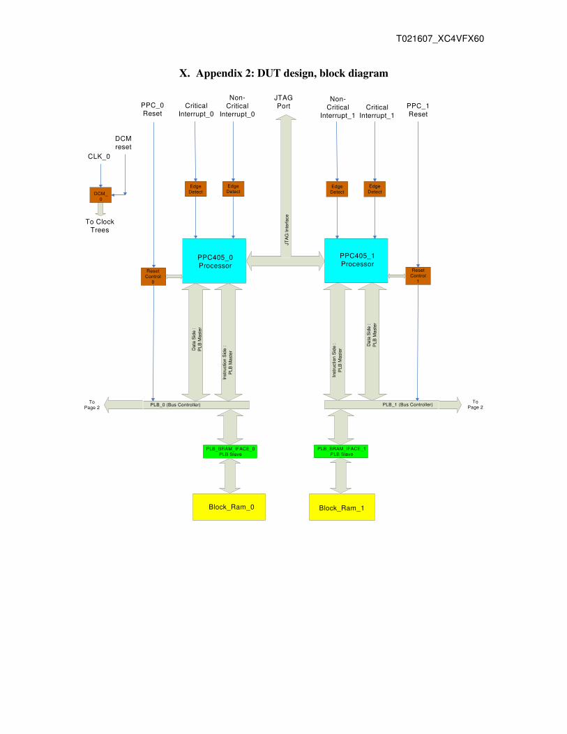
DUT design block diagram is shown in Appendix 2. It is basically made of the two XC4VFX60 embedded power PCs and one large shift register. The Power PC section of the DUT consists of two identical circuits each centered around one of the embedded power PC 405 processors. The tester feeds a single clock signal at a frequency of 62.5 MHz to the DUT. The processor runs at a frequency of 250 MHz generated by a local Digital Clock Manager (DCM). Each processor circuit contains a Processor Local Bus (PLB) that is the main memory bus of the processor and runs at 62.5 MHz. Each Power PC interfaces with one of the 2Mx16 SRAM banks on the DUT daughter board. External SRAMs on daughter board house both the instruction memory and data memory for all operations of the power PCs.
Each processor communicates to the tester board either through a UART that is
attached to an On chip Peripheral Bus (OPB) connected to the PLB by a PLB to OPB bridge or through a high speed parallel port. Via this port the tester board can access directly the external SRAMs banks through a multiplexer within the DUT.
One version of the design includes the Xilinx self-scrubbing of configuration memory with on chip Internal Configuration Access Port (ICAP).
Separately from the power PC circuits, a shift register made of 8 chains of 2000
flip-flops was implemented. Each shift register runs at 125 Mhz with a 4-bit parallel output operating at 31.25 Mhz representing the next 4 bits of the shift register. These shift registers are presented to the tester board as a 32-bit word with an associated 31.25 Mhz shift_clock.
Design utilization of XC4VFX60 resources is shown in Appendix 3. Shift register
uses most of the flip-flops. Without the shift register, only 7% of available flipf-flops would be used. Two different test programs have been used: - Multi interrupt or “ping-pong” program: Each PPC simply waits for a critical or non-
critical interrupt. Then, when the interrupt is received, a counter is incremented corresponding to the types of interrupt that is received and a message is sent out through the UART or high speed parallel port to HSDT board. The format of these messages is described in Appendix 4.
- One critical interrupt program: Tester sends a critical interrupt to each processor. This starts a principal counting program. Format of data sent to the HSDT is shown in Appendix 4.
During irradiation, DUT power supply currents (Vccint (1.2V), Vccaux(2.5V),
and Vcco(3.3V)) were monitored. Nominal DUT power supply currents are 440 mA, 70 mA, and 95 mA for Vccint, Vccaux, and Vcc0 respectively. As soon as one of the current reaches a programmable SEL detection level (750 mA for core, 500 mA for aux, and 500mA for I/O), the DUT power supplies were shutdown and irradiation was stopped.

T021607_XC4VFX60
DUT die temperature was measured via the DUT internal temperature sensing diode. Power supply and temperature monitoring and control are performed with a Labview program running on a laptop.
Another Labview program running on another laptop interfaced with HSDT. It set
test modes and collects telemetry. HSDT program performed two tasks during the irradiation. Shift register was exercised but not tested:
- Scrub of DUT configuration memory: all configuration memory but BRAM is scrubbed at a frequency of 31 MHz, scrubbing command is a manual command from Labview program. Test can be run with and without scrubbing. The time between scrubs is programmable. This scrub is a blind scrub that does not rely on readback and analysis of readback frame CRC as scrubbing can be done by other teams. DUT configuration is stored in HSDT SRAM and each configuration 32 bit word is rewritten every 15 ms.
- Test of the two power PCs in DUT. With the multi-interrupt test program, the HSDT program sends regularly (time between interrupts is programmable) interrupt request (critical and non critical) to each power PC, collects the processor response to this interrupt requests and sends the messages to the Labview program. If one of the power PC hangs (no response to interrupt request), a timeout signal is sent to the Labview program. With the “one critical interrupt” program, HSDT program send one critical interrupt to each power PC, then it collects the data from the processor. When data stop coming, a timeout signal is sent to the Labview program. Test start is a manual command from Labview program.
Test commands of HSDT program are shown in Appendix 5. Test procedure is a follows. In case of an event (time out or SEL) irradiation is stopped, and the following sequence is applied:
- reset PPC and restart PPC (manual Labview commands) If DUT is up and running again, another irradiation run can be started. If it does not work:
- Reset DUT and restart DUT (manual Labview commands) If DUT is up and running again, another irradiation run can be started. If it does not work:
- Unconfigure and reconfigure DUT (manual Labview commands) If DUT is up and running again, another irradiation run can be started. If it does not work:
- Reload test programs in SRAMs If DUT is up and running again, another irradiation run can be started. If it does not work:
- Power cycle DUT and reconfigure If DUT is up and running again, another irradiation run can be started. If it does not work:
- Resend DUT configuration bit file to the tester and reconfigure DUT

T021607_XC4VFX60
If DUT is up and running again, another irradiation run can be started. If it does not work:
- Power cycle tester board and DUT, reconfigure tester and DUT If DUT is up and running again, another irradiation run can be started After each irradiation run, content of DUT configuration memory was readback with Xilinx IMPACT software tool. IMPACT allows configuration, readback of configuration memory, and readback with verify though JTAG interface. IMPACT does the verification of configuration memory with a CRC code. List of test equipment is presented in Appendix 6.
VII. Test Results
No SEL was observed during the experiments up to the maximum tested LET of 58 MeVcm2/mg. The high current jumps observed on I/O power supply during previous tests at MSU1 and IUCF2 were not observed during these tests. We irradiated a delidded SRAM on DUT board, and we observed the same high-current jumps. This confirms that these jumps are due to microlatchup events in Cypress SRAMs on DUT board (see Figure 3) and do not come from XC4VFX60 FPGA. Cypress SRAMs mounted on DUT board share their 3.3V power supply with DUT I/O power supply. At MSU, ion penetration range was long enough to go through Cypress SRAMs plastic package and reach device sensitive areas. Cypress SRAM micro latchup sensitivity is high enough to be induced by protons2.
Table 2 shows a summary of test results obtained with multi-interrupt test
program. We started the tests with multi-interrupts program and a data transfer from DUT to tester via RS232 port. Time interval between interrupt requests was 1 second. It is not possible to send interrupt requests faster when using serial port without losing data. Then, we performed the same test using a data transfer from DUT to tester via high-speed port. As expected and shown in Figure 4 similar SEFI cross-sections were observed. The advantage of using the high-speed port is that we can reduce the time interval between interrupt requests without losing test data.
1 Heavy ion SEL test of Virtex-4 FPGA XC4VFX60 from Xilinx, test report, February 2007. 2 Proton SEL test of Virtex-4 FPGA XC4VFX60 from Xilinx, test report, February 2007.

T021607_XC4VFX60
Table 2: Summary of test results
SN #
Scrub
Time between
IT intervals (ms)
Ion
LET (MeVcm2/mg)
Tilt
eff. LET (MeVcm2/mg)
fluence (#/cm2)
SEFI #
X SEFI (cm2/dev)
CLmax (cm2/dev)
CLmin (cm2/dev)
S3 no 1000 Ar 5.7 0 5.71 4.84E+04 10 2.07E-04 3.50E-04 1.12E-04 S3 no 1000 Ar 5.7 45 8.06 6.18E+04 10 1.62E-04 2.74E-04 8.78E-05 S3 no 1000 Kr 20.6 45 29.13 3.80E+03 5 1.32E-03 2.77E-03 5.19E-04 no 1 Ar 5.7 0 5.70 1.60E+04 5 3.12E-04 6.56E-04 1.23E-04
S3 no 100 Ar 5.7 0 5.70 8.00E+04 10 1.25E-04 2.12E-04 6.78E-05 S3 no 100 Ar 5.7 0 5.70 8.25E+03 2 2.42E-04 7.63E-04 4.31E-05 S3 no 100 Ar 5.7 45 8.06 6.16E+03 3 4.87E-04 1.26E-03 1.33E-04
S2-S3 no 100 Kr 20.6 0 20.60 1.68E+04 11 6.53E-04 1.08E-03 3.66E-04 S2-S3 100 Kr 20.6 45 29.13 3.25E+03 9 2.77E-03 4.84E-03 1.45E-03
S2 no 100 Xe 40.7 0 40.70 1.20E+03 3 2.50E-03 6.47E-03 6.83E-04 S2 no 100 Xe 40.7 45 57.56 1.05E+03 4 3.80E-03 8.70E-03 1.30E-03 S3 external 1000 Kr 20.6 45 29.13 4.34E+04 3 6.91E-05 1.79E-04 1.88E-05 S3 external 1 Ar 5.7 0 5.70 3.12E+04 5 1.60E-04 3.36E-04 6.31E-05 S3 external 100 Ar 5.7 0 5.70 3.68E+05 10 2.72E-05 4.61E-05 1.47E-05 S3 external 100 Ar 5.7 0 5.70 4.09E+04 2 4.89E-05 1.54E-04 8.69E-06 S3 external 100 Ar 5.7 45 8.06 2.85E+04 3 1.05E-04 2.72E-04 2.87E-05
S2-S3 external 100 Kr 20.6 0 20.60 7.55E+04 10 1.32E-04 2.25E-04 7.19E-05 S2-S3 external 100 Kr 20.6 45 29.13 1.41E+04 8 5.66E-04 1.02E-03 2.82E-04
S2 external 100 Xe 40.7 0 40.70 6.42E+03 4 6.23E-04 1.43E-03 2.13E-04 S2 external 100 Xe 40.7 45 57.56 6.91E+03 4 5.79E-04 1.32E-03 1.98E-04 S3 self (ICAP) 1 Ar 5.7 0 5.70 3.67E+04 6 1.63E-04 3.22E-04 7.11E-05 S3 self(ICAP) 100 Ar 5.7 0 5.70 1.55E+05 10 6.47E-05 1.10E-04 3.51E-05
1.00E-05
1.00E-04
1.00E-03
4.00 5.00 6.00 7.00 8.00 9.00 10.00
Effective LET (MeVcm2/mg)
SE
FI C
ross
-sec
tion
(cm
2 /dev
ice)
RS232 1s, no scrubHigh-speed 1s, no scrubSeries2
Figure 4: SEFI cross-sections, multi-interrupt program, 1s interval between interrupts,
RS232 versus high-speed data transfer

T021607_XC4VFX60
Figure 5 shows SEFI cross-sections versus interval time between interrupts. We can see that SEFI cross-sections increase when time interval between interrupt requests decreases. The effect is more significant at high LET and with scrubbing.
Figure 6 shows SEFI cross-section with a time interval between interrupt requests of 100 ms. SEFI cross-sections are very high compared to SEFI on commercial Power PC chips available on the market3. Figure 6 shows that external scrub provides a significant improvement. SEFI cross-sections are reduced by about one order of magnitude. Self-scrub provides only marginal improvement.
Figure 5: SEFI cross-sections versus interval time between interrupt requests
3 F. Irom &al., “Single-Event Upset and Scaling Trends in New Generation of the Commercial SOI Power PC Microprocessors,” IEEE Trans. on Nuc. Sci., vol. 53, n˚6, December 2006

T021607_XC4VFX60
1.00E-06
1.00E-05
1.00E-04
1.00E-03
1.00E-02
0 10 20 30 40 50 60 70
LET (MeVcm2/mg)
SE
FI c
ross
sec
tion
(cm
2 /dev
)
no scrubexternal scrubself scrubno scrub CL
Figure 6: SEFI cross-sections for an interval time
between interrupt requests of 100 ms.
We can also a difference in the way the part is recovering from SEFI. In all cases, no power cycle was necessary to recover from SEFI. In most cases, it was necessary to reconfigure DUT and reload test programs in external SRAMs. This means that the SEFI caused a corruption of data and code stored in external SRAMs. Figure 7 shows that 100% of SEFIs needed a reconfiguration and a reload of test programs in external SRAMs to recover from when DUT configuration memory was not scrubbed. Without scrubbing, FPGA is going down before the PPCs.
No scrub
Reconfigure + reload SRAMReset PPCReset DUT
Figure 7: recoveries from SEFI when DUT
configuration memory is not scrubbed

T021607_XC4VFX60
Figure 8 shows the SEFI recovery modes when the DUT was self-scrubbed. We can see that in 13% of the cases, a PPC reset is sufficient to recover from SEFI. In these cases we have an actual SEFI within the PPC (corruption of command registers, program counters, stacks,….) before the FPGA is going down.
Self scrub
Reconfigure + reload SRAMReset PPCReset DUT
Figure 8: recoveries from SEFI when DUT
configuration memory is self-scrubbed
Figure 9 shows the SEFI recovery modes when DUT configuration memory is externally scrubbed. We can see that in about 50% of the cases a reset PPC is sufficient to recover from. In one occurrence, a reset DUT was sufficient to recover from a SEFI condition. With the external scrub we have about as much SEFI within the PPC than within the FPGA fabric.
External scrub
Reconfigure + reload SRAMReset PPCReset DUT
Fig 9: recoveries from SEFI when DUT configuration
memory is scrubbed externally

T021607_XC4VFX60
The external scrub is a blind scrub that does not rely on any coding. It can correct any kind of error. External scrub frequency is 32 MHz. So every configuration 32-bit word will be scrubbed every 15 ms (BRAM is not scrubbed).
Self-scrub is based on a Single Error Correct Double Error Detect (SECDED) EDAC. Therefore, multiple errors within a 32 bits word will not be corrected. ICAP gives the information about the occurrence of multiple errors detected, Single errors detected, and Single errors corrected. Table 3 shows these counts for some runs with self-scrub. We can see extremely large multiple errors counts. However, it should be noted that this count is not the actual count of multiple errors in configuration memory. Once a multiple error is detected, it would be counted every time the scrubber reads the same word because it can’t correct the error. Self-scrub has a frequency of 100MHz. It is significantly faster than external scrub. Every 32-bit word will be scrubbed every 5 ms. However, when an error is detected is takes about 100 ms to fix. Assuming a configuration memory sensitive cross-section of about 0.1 cm2 at the LET of 5.7 MeVcm2/mg, the error rates during the irradiation runs were between 1 per 60 ms (flux 168 #/cm2-s) and 1 per 190 ms (flux of 52 #/cm2-s). It is possible that the self-scrub was overwhelmed by this error rate and would have performed better at a slower error rate.
Table 3: Multiple errors detect, Single error detect, and
Single error correct counts for some runs with self-scrub
RUN #
Time between
IT intervals (ms)
Eff LET (MeVcm2/mg)
Flux (#/cm2-s)
Fluence (#/cm2)
SEFI #
X SEFI (cm2/dev)
Comment
Multiple Error detect
Single error
detect
Single error
correct 192 1 5.70 66 1.84E+03 1 5.43E-04 PPC0 down 9632 6 5 194 1 5.70 64 1.07E+03 1 9.35E-04 PPC1 down 5925 22 21 196 1 5.70 67 2.33E+04 1 4.29E-05 PPC0 down 2783 22 20 197 1 5.70 63 9.59E+02 1 1.04E-03 PPC1 down 4859 39 39 162 100 5.70 168 1.71E+04 1 5.85E-05 PPC1&0down 51156 19 18 163 100 5.70 160 6.38E+03 1 1.57E-04 PPC0 down 33630 21 19 164 100 5.70 164 2.32E+03 1 4.31E-04 PPC1 down 5515 8 5 167 100 5.70 52 1.00E+03 1 1.00E-03 PPC0 down 19378 15 14 168 100 5.70 57 2.12E+03 1 4.72E-04 PPC0 down 3157 13 13
A SEFI in our test is defined as a timeout when one of the two PPC does not answer to interrupt requests. Other test teams4 report Power On Reset (POR) SEFI and Select MAP (SMAP) SEFI. POR SEFI are detected if Done pin goes low, all configuration logic is reset, or if all configuration control registers are reset to a preconfigured state. SMAP SEFIs are detected by an inability to read/write configuration memory.
Done pin never went down during all test performed. In one occurrence only (run 193), we observed an extremely large number of errors in the readback file stored at the 4 G. Allen & al., “Initial Upset Measurements on a Virtex-4 FPGA Incorporating 90 nm Features and Thin Epitaxial Layer,” presented at SEE Symposium 2007, Long Beach, CA, April 2007.

T021607_XC4VFX60
end of irradiation. Even though IMPACT count of readback errors is not accurate, this may be an indicator of a POR SEFI.
As we don’t perform readback during irradiation, the only way to see a SMAP SEFI is when we have an external scrub. A SMAP SEFI would make the scrubbing not working. Therefore, SEFI cross-section would be similar to the SEFI cross-section without scrub. We never saw that during all our tests.
Maximum measured cross-section for POR and SMAP SEFI is about 2E-6 cm2/device4. It is 2 to 3 orders of magnitude lower than the SEFI cross-sections measured during this test. As we stopped the irradiations runs as soon as a SEFI occurred, we had a little chance to observe POR and SMAP SEFI during these tests.
A new high-current mode was also reported4. This event had a very low cross-section, one order of magnitude less than POR and SMAP SEFIs. Among the hundred plus irradiation runs performed during these tests, we only observed one irradiation run with a current jump on core current. Figure 10 shows the DUT power supply currents recorded during this run. The condition disappeared after DUT reconfiguration. A probable cause for this jump is a configuration bit upset that caused a signal contention in the circuit.
Run 73, external scrub, LET=20.6 MeVcm2/mg
0.00E+00
5.00E-01
1.00E+00
1.50E+00
2.00E+00
2.50E+00
3.00E+00
1 13 25 37 49 61 73 85 97 109
121
133
145
157
169
181
193
205
217
229
241
253
265
277
289
301
313
325
337
349
361
Time
Pow
er S
uppl
y cu
rren
t (A
)
IcoreIauxIio
Figure 10: Current profiles for run 73
We performed a few runs using PPC cache memory. Results are summarized in Figure 11. We can see a small increase of SEFI cross-section when cache memory is used.

T021607_XC4VFX60
0.00E+00
5.00E-05
1.00E-04
1.50E-04
2.00E-04
2.50E-04
3.00E-04
3.50E-04
Scrub no cache Scrub cache No scrub no cache No scrub cache
SE
FI C
ross
-sec
tion
(cm
2 /dev
)
Figure 11: Effect of cache memory on SEFI cross-sections, LET=5.7 MeVcm2/mg,
Time interval between IT requests=100 ms
An analysis of data files showed that there were only a few data errors. We see the SEFI before we see data errors. It should be noted that our test program that increments 2 counters for each PPC, one for each type of interrupt, critical and non critical, is not data intensive. More errors are expected on a data intensive application.
As noted before, after each irradiation run we read back configuration memory via JTAG interface and stored it for further analysis. Unfortunately, we could not use IMPACT because it uses CRC to verify and correct. Therefore, it can only work for a handful of errors. IMPACT Verify tool was intended on use while configuring the device, not to check the number of errors after an irradiation. We sent a subset of our files to Xilinx for analysis. Results are summarized in Table 4. Table 4 gives the error cross-sections in configuration memory per resource: routing bits, Look Up Tables, BRAM, and other miscellaneous resources. Figure 12 shows a plot for the LET of 5.7 MeVcm2/mg.
Table 4: summary of readback file analysis
LET (MeVcm2/mg) Scrub
conf/ routing cross-section
(cm2/dev)
LUT cross-section
(cm2/dev)
BRAM cross-section
(cm2/dev)
Misc cross-section
(cm2/dev) 5.7 no 3.05E-02 6.00E-02 6.32E-01 2.97E-03
8.06 no 7.13E-02 3.38E-01 2.11E+00 5.85E-03 5.7 external 0.00E+00 2.67E-03 7.63E-02 0.00E+00
8.06 external 0.00E+00 1.03E-02 3.81E-01 0.00E+00 5.7 self 2.00E-02 1.24E-02 3.16E-01 1.96E-03

T021607_XC4VFX60
0.00E+00
1.00E-01
2.00E-01
3.00E-01
4.00E-01
5.00E-01
6.00E-01
7.00E-01
Error cross-sections (cm2/dev)
conf/routing LUT BRAM Misc.
no scrubself scrubexternal scrub
Figure 12: Error cross-sections in configuration memory per resource
If we look at the routing bits, we can see that self-scrub only gives marginal improvement. Theoretically the number of errors with self-scrub should be the number of uncorrectable errors or multiple bit upsets (MBU) within a 32 bit word. According to the results in Table 4, the proportion of MBU would be 60%. This number is too high for a LET of 5.7 MeVcm2/mg, if published data on Virtex-4 is accurate5. This is another indication that the self-scrub could not catch-up with the error rate even at the low ion fluxes used for these tests. With the external scrub we did not get any error in the routing bits. This is a great demonstration of the efficiency of external scrub. The same observations apply to the miscellaneous resources bits.
If we look at the LUT, we can see that the number of errors, and, therefore, the cross-sections are higher even though the number of LUT bits is significantly lower than the number of routing bits (about 1.55E7 routing bits for 395K LUT bits). An explanation for this is that some LUT, LUTRAM, are dynamic. If a design uses these LUTRAM, the bits will change when the circuit is exercised. This applies for SRL16 registers as well. Also these LUTRAM and SRL16 cannot be scrubbed (at least by our external blind scrub that rewrite the original state) without impairing design functionality. This is the reason why we still have some remaining differences with the initial state at configuration even with the external scrub. We can’t explain why we always have the same number of
5 H. Quinn, “Eight years of MBU Data: What Does it all Mean?,” SEE Symposium 2007, Long Beach, CA, April 2007.

T021607_XC4VFX60
errors, though (we always got 98 errors in LUT on 13 different runs at different fluences for two LET values with the external scrub).
If we look at BRAM, we can see a significant difference in the number of errors for the different scrub modes, even though BRAM is never scrubbed. The reason for this is that some configuration/routing bits affect BRAM. There are the redundant column self-repair (256bits), the latch mode bit (9216 bits), as well as bits controlling the width, mode, and ports. Therefore, when these configuration bits are in error, the numbers of errors in BRAM looks higher than he actually is.
Table 6 gives total bit error cross-section for configuration bits and BRAM bits. Configuration bit error cross-section is obtained from the number of errors without scrubbing. BRAM bit error cross-section is obtained from the number of errors with external scrub (without any error in routing bits). We also excluded irradiation runs with abnormally high numbers of errors in BRAM. Number of BRAM bits is 4176 Kbits. BRAM bits are 8T cells. They are larger than 6T cells configuration bits. Memory cells are about twice the area of typical 6T and 8T cells.
Table 6: Bit error cross-sections
Effective LET (MeVcm2/mg)
conf/ routing cross-section
(cm2/bit)
BRAM cross-section
(cm2/bit) 5.7 1.97E-09 1.78E-08
8.06 4.60E-09 8.91E-08
VIII. Summary
XC4VFX60 Xilinx FPGA is not sensitive to Single Event Latchup up to the maximum tested LET of 58 MeVcm2/mg. SEFI sensitivity is high in comparison with commercial Power PC SEFI cross-sections. External scrub provides a significant improvement. Self-scrub is not very effective. Main reason is its inability to correct MBUs. It is also probable that test flux was too high for self-scrub capability. No other kind of SEFI was observed during these tests. In most cases recovery from SEFI is obtained via reconfiguration and reload of code stored in PPC external memories.

T021607_XC4VFX60
IX. Appendix 1: Electrical interfaces
a) Daughter board to main interface
FX60 Daughter Board interfaces with the main board, High Speed Digital Tester (HSDT), via 1156-pin Hi-Lo connector. There are TBD numbers of general purpose I/Os available for user. I/O standard can be any of Xilinx defined I/O standards. Beside general purpose I/Os, there are 8 data lines and 6 control lines available for Select MAP programming of FX60. Figure 1 depicts the block diagram of FX60 test setup electrical interface.
Hi-Lo Interface
FX60
JTAG Header
PROM
Mode Select
External Power
(Optional)
General I/O
Select MAP
Power
Power Supply Power Supply or DMM
(Optional)
PC
Interface (RS232)
Program Voltage
Regulator (PT6701)
JTAG
Header
Hi-Lo Interface
FPGA (VII-Pro)
PROM
Voltage Regulators
HSDT
Controller (PC)
GPIB (PC)
Programmer
(PC)
Figure 1. Block Diagram of FX60 Test Setup Electical Interface
For Heating Unit
Heating Unit
FX60 Daughter Board
Thermistor/IR Dector
b) FX60 Daughter board Besides Hi-Lo interface connector to HSDT, JTAG programming connector,
Mode pins, and power supply connections are available for external connection. JTAG program connector is a 6-pin single strip header that can be connected to
PC via programming cable. JTAG connector is used to program the PROM (XCF32P) on the daughter board as well as FX60.
Mode pins select the FX60 programming mode, either Select MAP Program or Serial PROM Download. Mode pins are pull up jumpers that can be grounded using shorting plugs. HSDT can also select the programming mode if the jumpers are removed. This will allow the user to control the mode remotely.
Heating coils may be placed along the edge of FX60 if needed. This is to test the device at elevated temperature for latch up condition. High power resistors or Thermofoil heaters from Minco will be used for heating coils. The temperature of the device will be monitored by either thermistor or IR detector and controlled by the power supply to the coils.

T021607_XC4VFX60
The daughter board requires four power supplies (3.3V, 2.5V, 1.8V, and 1.2V) to FX60 and peripheral devices such as PROM and SRAM. The daughter board can be powered up by the HSDT’s programmable voltage regulators (PT6701) or by external power supplies. HDST supplies the power to the daughter board via Hi-Lo connector. Each supply line from Hi-Lo connector has set of jumpers in series. When these jumpers are shorted, the daughter board gets power from the HSDT regulators. The jumpers can be used to monitor device currents using a digital multi-meters in series or by using shunt resistors. To supply power to FX60 using external power supply, the shorting jumper should be removed and the required power should be connected to the jumper pins. Figure 2 shows the power options for FX60 daughter board.
Hi-Lo Interface
FX60 Daughter Board
In-Line Headers
From HSDT
To FX60 and others
Place jumper to enable power route from HSDT. DMM in series / or shunt resistor can be used to monitor current.
Jumpers may be removed and external supply can be brought in via these pins.
Figure 2. Power Options for FX60 Board
c) HSDT Connection
HSDT board is powered by single +5V supply via BNC. Onboard regulators will convert +5V to supply necessary powers to the board.
HSDT has RS232, USB and Ethernet connections for communication with an external PC. The PC is the controller that commands HSDT and collects data from HSDT. For the initial test of FX60, RS232 will be used.
HSDT’s main processor (VirtexII-Pro) can be programmed using JTAG connector or onboard PROM. The PROM is programmed via JTAG as well. JTAG connector for the HSDT is also a 6-pin single strip header.
T021607_XC4VFX60
X. Appendix 2: DUT design, block diagram
PPC405_0Processor
PPC405_1Processor
PLB_0 (Bus Controller) PLB_1 (Bus Controller)
Dat
a S
ide
: P
LB M
aste
r
PLB_BRAM_IFACE_0PLB Slave
PLB_BRAM_IFACE_1PLB Slave
Block_Ram_0
JTA
G In
terfa
ce
JTAG Port
ResetControl
0
ResetControl
1
DCM_0
To Clock Trees
CLK_0
ToPage 2
ToPage 2
Inst
ruct
ion
Sid
e :
PLB
Mas
ter
Inst
ruct
ion
Sid
e :
PLB
Mas
terD
ata
Sid
e :
PLB
Mas
ter
DCM reset
EdgeDetect
EdgeDetect
CriticalInterrupt_0
Non-Critical
Interrupt_0
EdgeDetect
EdgeDetect
PPC_0Reset
PPC_1Reset
CriticalInterrupt_1
Non-Critical
Interrupt_1
Block_Ram_1

T021607_XC4VFX60
PLB_0 (Bus Controller)
PLB_EMC_0(SRAM Controller)
PLB Slave
CEn, OEn, WEnADDR(0 to 20)
DQ(0 to 15)To
External SRAM Block 0
FromPage 1
CE
n, OE
n, WE
nA
DD
R(0 to 20)
DQ
(0 to 15)
SRAM_MUX_0
CE
n, OE
n, WE
nA
DD
R(0 to 20)
DQ
(0 to 15)
SRAM0 InterfaceFrom
Tester Board
SRAM_MUX_0Control fromTester Board
PLB_1 (Bus Controller)
PLB_EMC_1(SRAM Controller)
PLB Slave
CEn, OEn, WEnADDR(0 to 20)
DQ(0 to 15)To
External SRAM Block 1
FromPage 1
CE
n, O
En,
WE
nA
DD
R(0
to 2
0)D
Q(0
to 1
5)
SRAM_MUX_1
CE
n, O
En,
WE
nA
DD
R(0
to 2
0)D
Q(0
to 1
5)
SRAM1 InterfaceFrom
Tester Board
SRAM_MUX_1Control fromTester Board

T021607_XC4VFX60
Shift Registers(32 X 2000)
ToTesterBoard
FromDCM_0
CLK2X (125Mhz)
PLB_0 (Bus Controller)
HS_PORT_0(SRAM Controller)
PLB Slave
CEn, OEn, WEnDQ(0 to 31)
To External Tester Interface 0
FromPage 1
High-Speed (Parallel) Ports
PLB_1 (Bus Controller)
HS_PORT_1(SRAM Controller)
PLB Slave
CEn, OEn, WEnDQ(0 to 32)
To External Tester Interface 1
FromPage 1
High-Speed (Parallel) Ports

T021607_XC4VFX60
PLB_1 (Bus Controller) FromPage 1
PLB
_to_
OP
B_1
Brid
ge
OPB_1 (Bus Controller)
RS232_1(opb_uart_lite)
OPB Slave
RS232_1_RXRS232_1_TX
To Tester
Board
SERIAL PORTS

T021607_XC4VFX60
PLB_0 (Bus Controller)From
Page 1
PLB
_to_
OP
B_0
Brid
ge
OPB_0 (Bus Controller)
RS232_0(opb_uart_lite)
OPB Slave
RS232_0_RXRS232_0_TX
To Tester
Board
SERIAL PORTS

T021607_XC4VFX60
ICAP/Frame_ECC
SEU Detection and Correction
ICAP / Frame ECC Control Logic
BRAM
Frame ECC Block ICAP
Self-Scrub Interface
ToTester

T021607_XC4VFX60
XI. Appendix 3: DUT design utilization of FPGA resources
Device Utilization Summary
Logic Utilization Used Available UtilizationNumber of Slice Flip Flops 19,652 50,560 38%Number of 4 input LUTs 3,412 50,560 6%Logic Distribution Number of occupied Slices 11,443 25,280 45% Number of Slices containing only related logic 11,443 3,433 100% Number of Slices containing unrelated logic 0 3,433 0%Total Number 4 input LUTs 4,150 50,560 8%Number used as logic 3,428Number used as a route-thru 138Number used for Dual Port RAMs 360Number used as Shift registers 224Number of bonded IOBs 277 576 48%Number of BUFG/BUFGCTRLs 3 32 9% Number used as BUFGs 3 Number used as BUFGCTRLs 0Number of FIFO16/RAMB16s 64 232 27% Number used as FIFO16s 0 Number used as RAMB16s 64Number of DCM_ADVs 1 12 8%Number of PPC405_ADVs 2 2 100%Number of DCIRESETs 1 1 100%Number of JTAGPPCs 1 1 100%Total equivalent gate count for design 4,414,652Additional JTAG gate count for IOBs 13,296
Additionally, the following resources are used when the ICAP controller is instantiated:
Design Summary for SEU_cntrl Target Device: 4vfx60ff1152-10Total Slices 156 25,280 .62% ? 1%Slice Flip Flops 153 50,560 .30% ? 1%Total LUTs 238 50,560 .47% ? 1%BRAMs 2 232 .86% ? 1%ICAP_VIRTEX4s 1 2 50%FRAME_ECC_VIRTEX4s 1 1 100%
Total equivalent gate count for ICAP instantiation: 10,359

T021607_XC4VFX60
XII. Appendix 4 Data formats
THERE ARE 2 PAGES TO THE FORMATS. ******** MEANS YOU ALREADY HAVE IT ---------------- RS232 DATA if (new_data_read = '1' and new_data_read_1q = '0') then ************ fx60_error_read(7 downto 0) <= fx60data; fx60_error_read(31 downto 16) <= error_stuffer ; fx60_error_read(32) <= sent_int ; fx60_error_read(33) <= sent_cint ; fx60_error_read(40) <= done_pin ; fx60_error_read(47 downto 41) <= (others=> '0'); fx60_error_read(71 downto 48) <=timeout_counter; fx60_error_read(79 downto 72) <= PC_NUMBER; new_data_write <= '1'; ------------------- HIGH Speed pingpong interrupts ******************************** elsif new_hs_data = '1' and (read_on = '0' or turn_all_on = '1') then fx60_error_read(31 downto 0) <=hs_data; fx60_error_read(32) <= sent_int ; fx60_error_read(33) <= sent_cint ; fx60_error_read(40) <= done_pin ; fx60_error_read(47 downto 41) <= (others=> '1'); fx60_error_read(71 downto 48) <= timeout_counter; fx60_error_read(79 downto 72) <= PC_NUMBER; new_data_write <= '1'; ---------------- HIGH SPEED (no ping pong – always write to hs post – just one crit int ) Counter after resync 16 times no luck must reset - all one’s come on elsif count_burst = 15 then fx60_error_read(79 downto 0) <= (others=> '1'); new_data_write <= '1'; elsif error_count_Reg = '1'then fx60_error_read(15 downto 0) <=hs_data(15 downto 0); fx60_error_read(31 downto 16) <=count_exp; fx60_error_read(32) <= sent_int ; fx60_error_read(33) <= sent_cint ; fx60_error_read(39 downto 36) <= count_burst ; fx60_error_read(40) <= done_pin ; fx60_error_read(47 downto 41) <= (others=> '1'); fx60_error_read(71 downto 48) <= timeout_counter; fx60_error_read(79 downto 72) <= PC_NUMBER; new_data_write <= '1'; ---------------------- Time out occurs – high speed elsif current_state = TM then************************************* fx60_error_read(39 downto 0) <=(others =>'0'); fx60_error_read(71 downto 41) <=(others =>'0'); fx60_error_read(40) <=done_pin; fx60_error_read(79 downto 72) <= PC_NUMBER; new_data_write <= '1';

T021607_XC4VFX60
-------------------Another timeout – high speed with counter elsif WATCH_DOG = CLK_ERROR AND ONE_MS = '1' then fx60_error_read(39 downto 0) <=(others =>'0'); fx60_error_read(71 downto 41) <=(others =>'0'); fx60_error_read(40) <=done_pin; fx60_error_read(77 downto 72) <= PC_NUMBER( 5 downto 0); fx60_error_read(79 downto 78) <= read_on & read_on; new_data_write <= '1'; else new_data_write <= '0'; end if; -------------------CHECK SHIFT REG COMMAND if ( error_start = '1' ) then shft_error_read_i(79 downto 72) <= x"03"; shft_error_read_i(31 downto 0) <= shft_data_read_ff; shft_error_read_i(63 downto 32) <= timer_ms; new_data_write_i <= '1'; ------------------- These are all self scan errors ------------------------ GOT ERROR AND WILL TRY TO FIX IT elsif got_error_scan = '1' and do_scan = '1' then shft_error_read_i(79 downto 72) <= x"0F"; shft_error_read_i(71 downto 24) <= time_scan; shft_error_read_i(23 downto 16) <= (others=> '1'); shft_error_read_i(15 downto 0) <= error_scan; new_data_write_i <= '1'; -------------- FIXED IT!!!!!!!!!!!!!!!!!!!!!!!!!!!!!!!!!!!!!!!!!!!!!!!!!!! elsif falling_SEU_DETECT = '1' then shft_error_read_i(79 downto 72) <= x"0E"; shft_error_read_i(71 downto 24) <= time_scan; shft_error_read_i(23 downto 16) <= (others=> '1'); shft_error_read_i(15 downto 0) <= error_scan; new_data_write_i <= '1'; -------------------------------- A RED LIGHT SHOULD LIGHT NO THIS ONE – MBUS HAVE OCCURRED AND CAN NOT BE FIXED: elsif scan_error_tester = '1' and do_scan = '1' then shft_error_read_i(79 downto 72) <= x"1F"; shft_error_read_i(71 downto 24) <= time_scan; shft_error_read_i(23 downto 0) <= (others=> '1'); new_data_write_i <= '1';

T021607_XC4VFX60
XIII. Appendix 5: Test procedures and commands
A. TESTS After a start test, a command 9 must be entered – this will start the interrupts. This was added so that clocks and resets occur (start test) but no interrupts until command.
1. Ping Pong : Test though highspeed port by interrupts Tester sends Interrupt to ppc0 then Interrupt to ppc1. Afterwards Critical Interrupt to ppc0 then Critical to ppc1. Data format corresponds to new_hs_data and read_on =’0’ (see format doc)
2. One Critical Interrupt Command 8 Tester only sends one interrupt. PPCs stay in interrupt routine and constantly write the high speed port. Happens about 270*8ns cycles. This is the test that pushes the pc’s because they are constantly working. This corresponds to error_count_reg. The tester will try to sync with the erroneous counter 16 times in a row (max). If it can not sync, then count_burst =15 and will cause ALL “1’s – you will need to reset the ppc.
3. Duration of Interrupts Command D0 has replaced command C0 – there is no longer an overlap.
4. Self Scrubbing See Mark for details. Command is AA. See format doc for new formats. There are 3 types of detects.
• SEU is detected(will start trying to correct) : got_error_scan • SEU that was detected has been corrected: SEU_DETECT • MBU – need to shut down: scan_error_tester = '1' and do_scan = '1'
B. Commands The major commands: Command HEX# MSB Byte1 Byte2 Byte3 Description Reset Dut 01 x x Start Test 02 x x x Starts critical interrupts and
data capture from PPC. Type of data capture is dependent on PPC software – tester will catch both serial and parallel
Start Interrupts 09 x x x SHOULD GO AFTER START TEST
HS Count 08 x x x High speed test – only one critical interrupt per ppc. PPC stays in interrupt routine and writes high speed port. MUST GO BEFORE START TEST
DCM RESET 0A x x x Generates dcm reset pulse Ppc0 reset 14 x x x Reset ppc0 No ppc0 reset 15 x x x Turn off reset of ppc0 Ppc1 reset 16 x x x Reset ppc1 No ppc1 reset 17 x x x Turn off reset of ppc1

T021607_XC4VFX60
Start_config 04 x x x Tester configures DUT Start scrub 06 x x x Tester scrubs dut via select
map Stop scrub 26 x x x Stop scrubbing – NOT
TESTED readback 05 x x x NOT TESTED Write_config 81 x x x Labview sends config bit file
to tester
Inject_error on 0E x x x Turn on error injection – need to set range first
Inject error off 0F x x x Turn off error
Milli_count B0 15 : 8 7 : 0 x MS Time between scrubbing – default = 0- timer starts at start of scrub – when expires and at end of scrub memory, scrubbing will start over
Error inj high mem address
7A 19 : 16 15:8 7:0 Address is the converted 32 bit address as stored in the tester SRAM. Divide actual config byte address by 4 to get mapped address. Inject error must be turned off to set this
Error inj low mem address
79 19 : 16 15:8 7:0 Address is the converted 32 bit address as stored in the tester SRAM. Divide actual config byte address by 4 to get mapped address- Inject error must be turned off to set this
Scrub_freq C0 3:0 x x 125MHz clock divider – default is 3. This determines the frequency of the select map clock to the DUT
Time_to_int D0 23: 16 15:8 7:0 Duration of an interrupt period (not cycle). The interrupt cycle is ¼ this speed (because 3 other interrupts occur). Default=020000
Self scrub AA x x x Turn on self scrubbing – only with ICAP design

T021607_XC4VFX60
C. Configure DUT
• Reset DUT • Send configdata to tester: command 81 and the config file – this sequence is in
labview and is not a miscellaneous command (optional if SRAM has already been written)
• Start configuration: command 4 x x x– Misc command D. Start Scrubbing
Before scrubbing is performed, a test should be done to validate that it is working. This can be done by the error inj commands and selecting a wide range of memory:
E. Debug • Reset dUT • 0F – turn off error inj • 79 00 00 00 – set error inj low address • 7A 07 00 00 – set error inj high address • 06 xx xx xx - turn on scrubbing • 0E – turn on error inj • Look for errors or done to disappear
F. Change Scrub Frequency Scrub Frequency (selectmap clock can be changed) The value is a clock divider. The clock is 125MHz. Therefore a value of 2 would be 62.5 (this speed has not been tested). Default is a divider of 3.
• C0 xN xx xx : N is the 4 LSB and should be greater than 2 (maybe 3) • Command 6 : start scrub
G. Change Scrub Cycle The scrubbing cycle is a window. Commence scrubbing at start of window. Scrubbing will stop at end of memory range. Scrubbing will begin at next window start. If window is smaller than time to scrub through memory, the scrubber will never stop. Default is to never stop.
• B0 : set mili_count- this is the size of the window in milliseconds • 06 : start scrub
H. Start Test After the DUT has been configured, start test can begin
• 01 xx xx xx - Reset DUT • 20 xx xx xx - PPC0 reset on (optional) • 22 xx xx xx - Ppc1 reset on (optional) • 21 xx xx xx - Ppc0 reset off (optional) • 23 xx xx xx - Ppc1 reset off (optional) • 06 xx xx xxTurn on scrubbing (optional) • 02 xx xx xx - Start test • 09 xx xx xx – start interrupts
Based on reset sequencing,

T021607_XC4VFX60
Appendix 6: Equipment list
- HSDT board - DUT daughter boards (x6) - Agilent N6700B power supply DUT - Agilent 6624A power supply - HP34401 multimeter - Xilinx JTAG probe - Keithley multimeter - Laptops (x3) - 100 feet Ethernet cable - 100 feet USB cable - router - GPIB cables - BNC cables