Embed Size (px)
Citation preview
MPC603/D(Motorola Order Number)
6/94REV
3
MPR603TSU-03(IBM Order Number)
™
603
Tech
nica
l Sum
mar
y
F
ree
sca
le S
em
ico
nd
uc
tor,
I
Freescale Semiconductor, Inc.n
c..
.
MICONDUCTOR, INC.
Advance InformationPowerPC™ 603 RISC MicroprocessorTechnical SummaryThis document provides an overview of the PowerPC 603™ microprocessor features,including a block diagram showing the major functional components. It also provides anoverview of the PowerPC Architecture™, and information about how the 603implementation complies with the architectural definitions.
This document is divided into three parts:
• Part 1, “PowerPC 603 Microprocessor Overview,” provides an overview of the 603 features, including a block diagram showing the major functional components.
• Part 2, “Levels of the PowerPC Architecture,” describes the three levels of the PowerPC architecture.
• Part 3, “PowerPC 603 Microprocessor: Implementation,” describes the PowerPC architecture in general, and specific details about the implementation of the 603 as a low-power, 32-bit member of the PowerPC processor family.
In this document, the terms “PowerPC 603 microprocessor” and “603” are used to denotethe second microprocessor from the PowerPC architecture family. The PowerPC 603microprocessors are available from IBM as PPC603 and from Motorola as MPC603.
ARCHIVED BY FREESCALE SE
used by Motorola under license from IBM Corp.PowerPC, PowerPC Architecture, POWER Architecture, PowerPC 603, and PowerPC 601 are trademarks of International Business Machines Corp.
This document contains information on a new product under development. Specifications and information herein are subject to change without notice.
© Motorola Inc. 1994Portions hereof © International Business Machines Corp. 1991–1994
For More Information On This Product,
Go to: www.freescale.com
F
ree
sca
le S
em
ico
nd
uc
tor,
I
Freescale Semiconductor, Inc.n
c..
.
Part 1 PowerPC 603 Microprocessor OverviewThis section describes the features of the 603, provides a block diagram showing the major functional units,and gives an overview of how the 603 operates.
The 603 is the first low-power implementation of the PowerPC microprocessor family of reduced instructionset computer (RISC) microprocessors. The 603 implements the 32-bit portion of the PowerPC architecture,which provides 32-bit effective addresses, integer data types of 8, 16, and 32 bits, and floating-point datatypes of 32 and 64 bits. For 64-bit PowerPC microprocessors, the PowerPC architecture provides 64-bitinteger data types, 64-bit addressing, and other features required to complete the 64-bit architecture.
The 603 provides four software controllable power-saving modes. Three of the modes (the nap, doze, andsleep modes) are static in nature, and progressively reduce the amount of power dissipated by the processor.The fourth is a dynamic power management mode that causes the functional units in the 603 toautomatically enter a low-power mode when the functional units are idle without affecting operationalperformance, software execution, or any external hardware.
The 603 is a superscalar processor capable of issuing and retiring as many as three instructions per clock.Instructions can execute out of order for increased performance; however, the 603 makes completion appearsequential.
The 603 integrates five execution units—an integer unit (IU), a floating-point unit (FPU), a branchprocessing unit (BPU), a load/store unit (LSU), and a system register unit (SRU). The ability to execute fiveinstructions in parallel and the use of simple instructions with rapid execution times yield high efficiencyand throughput for 603-based systems. Most integer instructions execute in one clock cycle. The FPU ispipelined so a single-precision multiply-add instruction can be issued every clock cycle.
The 603 provides independent on-chip, 8-Kbyte, two-way set-associative, physically addressed caches forinstructions and data and on-chip instruction and data memory management units (MMUs). The MMUscontain 64-entry, two-way set-associative, data and instruction translation lookaside buffers (DTLB andITLB) that provide support for demand-paged virtual memory address translation and variable-sized blocktranslation. The TLBs and caches use a least recently used (LRU) replacement algorithm. The 603 alsosupports block address translation through the use of two independent instruction and data block addresstranslation (IBAT and DBAT) arrays of four entries each. Effective addresses are compared simultaneouslywith all four entries in the BAT array during block translation. In accordance with the PowerPC architecture,if an effective address hits in both the TLB and BAT array, the BAT translation takes priority.
The 603 has a selectable 32- or 64-bit data bus and a 32-bit address bus. The 603 interface protocol allowsmultiple masters to compete for system resources through a central external arbiter. The 603 provides athree-state coherency protocol that supports the exclusive, modified, and invalid cache states. This protocolis a compatible subset of the MESI (modified/exclusive/shared/invalid) four-state protocol and operatescoherently in systems that contain four-state caches. The 603 supports single-beat and burst data transfersfor memory accesses; it also supports both memory-mapped I/O and direct-store interface addressing.
The 603 uses an advanced, 3.3-V CMOS process technology and maintains full interface compatibility withTTL devices.
1.1 PowerPC 603 Microprocessor FeaturesThis section describes details of the 603’s implementation of the PowerPC architecture. Major features ofthe 603 are as follows:
• High-performance, superscalar microprocessor
— As many as three instructions issued and retired per clock
— As many as five instructions in execution per clock
ARCHIVED BY FREESCALE SEMICONDUCTOR, INC.
2 PowerPC 603 RISC Microprocessor Technical Summary For More Information On This Product,
Go to: www.freescale.com
F
ree
sca
le S
em
ico
nd
uc
tor,
I
Freescale Semiconductor, Inc.n
c..
.
— Single-cycle execution for most instructions
— Pipelined FPU for all single-precision and most double-precision operations
• Five independent execution units and two register files
— BPU featuring static branch prediction
— A 32-bit IU
— Fully IEEE 754-compliant FPU for both single- and double-precision operations
— LSU for data transfer between data cache and GPRs and FPRs
— SRU that executes condition register (CR) and special-purpose register (SPR) instructions
— Thirty-two GPRs for integer operands
— Thirty-two FPRs for single- or double-precision operands
• High instruction and data throughput
— Zero-cycle branch capability (branch folding)
— Programmable static branch prediction on unresolved conditional branches
— Instruction fetch unit capable of fetching two instructions per clock from the instruction cache
— A six-entry instruction queue that provides look-ahead capability
— Independent pipelines with feed-forwarding that reduces data dependencies in hardware
— 8-Kbyte data cache—two-way set-associative, physically addressed; LRU replacement algorithm
— 8-Kbyte instruction cache—two-way set-associative, physically addressed; LRU replacement algorithm
— Cache write-back or write-through operation programmable on a per page or per block basis
— BPU that performs CR look-ahead operations
— Address translation facilities for 4-Kbyte page size, variable block size, and 256-Mbyte segment size
— A 64-entry, two-way set-associative ITLB
— A 64-entry, two-way set-associative DTLB
— Four-entry data and instruction BAT arrays providing 128-Kbyte to 256-Mbyte blocks
— Software table search operations and updates supported through fast trap mechanism
— 52-bit virtual address; 32-bit physical address
• Facilities for enhanced system performance
— A 32- or 64-bit split-transaction external data bus with burst transfers
— Support for one-level address pipelining and out-of-order bus transactions
— Bus extensions for direct-store interface operations
• Integrated power management
— Low-power 3.3-volt design
— Internal processor/bus clock multiplier that provides 1/1, 2/1, 3/1, and 4/1 ratios
— Three power saving modes: doze, nap, and sleep
— Automatic dynamic power reduction when internal functional units are idle
• In-system testability and debugging features through JTAG boundary-scan capability
ARCHIVED BY FREESCALE SEMICONDUCTOR, INC.
PowerPC 603 RISC Microprocessor Technical Summary 3 For More Information On This Product,
Go to: www.freescale.com
F
ree
sca
le S
em
ico
nd
uc
tor,
I
Freescale Semiconductor, Inc.n
c..
.
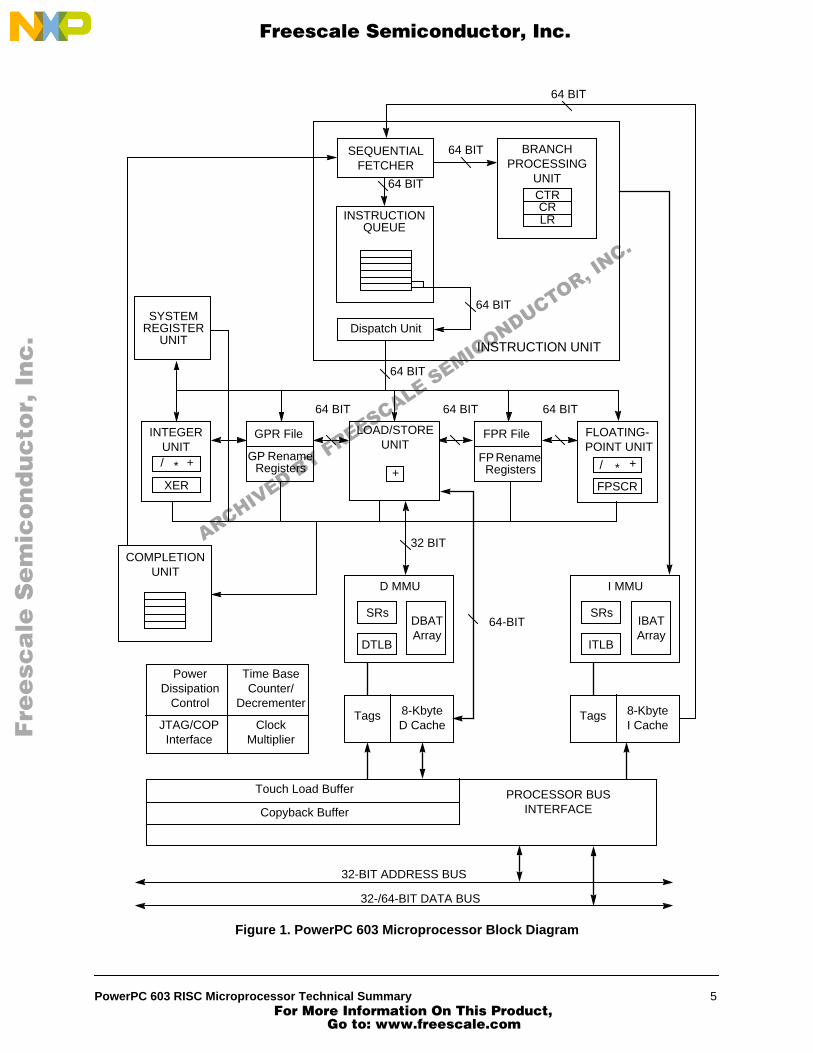
1.2 Block DiagramFigure 1 provides a block diagram of the 603 that illustrates how the execution units—IU, FPU, BPU, LSU,and SRU—operate independently and in parallel.
The 603 provides address translation and protection facilities, including an ITLB, DTLB, and instructionand data BAT arrays. Instruction fetching and issuing is handled in the instruction unit. Translation ofaddresses for cache or external memory accesses are handled by the MMUs. Both units are discussed inmore detail in Sections 1.3, “Instruction Unit,” and 1.5.1, “Memory Management Units (MMUs).”
1.3 Instruction UnitAs shown in Figure 1, the 603 instruction unit, which contains a fetch unit, instruction queue, dispatch unit,and BPU, provides centralized control of instruction flow to the execution units. The instruction unitdetermines the address of the next instruction to be fetched based on information from the sequential fetcherand from the BPU.
The instruction unit fetches the instructions from the instruction cache into the instruction queue. The BPUextracts branch instructions from the fetcher and uses static branch prediction on unresolved conditionalbranches to allow the instruction unit to fetch instructions from a predicted target instruction stream whilea conditional branch is evaluated. The BPU folds out branch instructions for unconditional branches orconditional branches unaffected by instructions in progress in the execution pipeline.
Instructions issued beyond a predicted branch do not complete execution until the branch is resolved,preserving the programming model of sequential execution. If any of these instructions are to be executedin the BPU, they are decoded but not issued. Instructions to be executed by the FPU, IU, LSU, and SRU areissued and allowed to complete up to the register write-back stage. Write-back is allowed when a correctlypredicted branch is resolved, and instruction execution continues without interruption along the predictedpath.
If branch prediction is incorrect, the instruction unit flushes all predicted path instructions, and instructionsare issued from the correct path.
ARCHIVED BY FREESCALE SEMICONDUCTOR, INC.
4 PowerPC 603 RISC Microprocessor Technical Summary For More Information On This Product,
Go to: www.freescale.com
F
ree
sca
le S
em
ico
nd
uc
tor,
I
Freescale Semiconductor, Inc.n
c..
.
Figure 1. PowerPC 603 Microprocessor Block Diagram
BRANCH PROCESSING
UNIT
32-/64-BIT DATA BUS
32-BIT ADDRESS BUS
INSTRUCTION UNIT
INTEGERUNIT
FLOATING- POINT UNIT
FPR File
FP Rename Registers
8-KbyteD Cache
Tags
SEQUENTIAL FETCHER
CTRCRLR
+*/
FPSCR
SYSTEM REGISTER
UNIT
+*/
PROCESSOR BUS INTERFACE
D MMU
SRs
DTLB
DBATArray
Touch Load Buffer
Copyback Buffer
64 BIT
32 BIT
Dispatch Unit
64 BIT
64 BIT
Power Dissipation
Control
COMPLETION UNIT
Time Base Counter/
Decrementer
ClockMultiplier
JTAG/COPInterface
XER
I MMU
SRs
ITLB
IBATArray
8-KbyteI Cache
Tags
64 BIT
64 BIT
64 BIT
64 BIT64 BIT
GPR File LOAD/STORE UNIT
+
64-BIT
GP Rename Registers
INSTRUCTIONQUEUE
ARCHIVED BY FREESCALE SEMICONDUCTOR, INC.
PowerPC 603 RISC Microprocessor Technical Summary 5 For More Information On This Product,
Go to: www.freescale.com

F
ree
sca
le S
em
ico
nd
uc
tor,
I
Freescale Semiconductor, Inc.n
c..
.
1.3.1 Instruction Queue and Dispatch UnitThe instruction queue (IQ), shown in Figure 1, holds as many as six instructions and loads up to twoinstructions from the instruction unit during a single cycle. The instruction fetch unit continuously loads asmany instructions as space in the IQ allows. Instructions are dispatched to their respective execution unitsfrom the dispatch unit at a maximum rate of two instructions per cycle. Dispatching is facilitated to the IU,FPU, LSU, and SRU by the provision of a reservation station at each unit. The dispatch unit performs sourceand destination register dependency checking, determines dispatch serializations, and inhibits subsequentinstruction dispatching as required.
For a more detailed overview of instruction dispatch, see Section 3.7, “Instruction Timing.”
1.3.2 Branch Processing Unit (BPU)The BPU receives branch instructions from the fetch unit and performs CR look-ahead operations onconditional branches to resolve them early, achieving the effect of a zero-cycle branch in many cases.
The BPU uses a bit in the instruction encoding to predict the direction of the conditional branch. Therefore,when an unresolved conditional branch instruction is encountered, the 603 fetches instructions from thepredicted target stream until the conditional branch is resolved.
The BPU contains an adder to compute branch target addresses and three user-control registers—the linkregister (LR), the count register (CTR), and the CR. The BPU calculates the return pointer for subroutinecalls and saves it into the LR for certain types of branch instructions. The LR also contains the branch targetaddress for the Branch Conditional to Link Register (bclrx) instruction. The CTR contains the branch targetaddress for the Branch Conditional to Count Register (bcctrx) instruction. The contents of the LR and CTRcan be copied to or from any GPR. Because the BPU uses dedicated registers rather than GPRs or FPRs,execution of branch instructions is largely independent from execution of integer and floating-pointinstructions.
1.4 Independent Execution UnitsThe PowerPC architecture’s support for independent execution units allows implementation of processorswith out-of-order instruction execution. For example, because branch instructions do not depend on GPRsor FPRs, branches can often be resolved early, eliminating stalls caused by taken branches.
In addition to the BPU, the 603 provides four other execution units and a completion unit, which aredescribed in the following sections.
1.4.1 Integer Unit (IU)The IU executes all integer instructions. The IU executes one integer instruction at a time, performingcomputations with its arithmetic logic unit (ALU), multiplier, divider, and integer exception register (XER).Most integer instructions are single-cycle instructions. Thirty-two general-purpose registers are provided tosupport integer operations. Stalls due to contention for GPRs are minimized by the automatic allocation ofrename registers. The 603 writes the contents of the rename registers to the appropriate GPR when integerinstructions are retired by the completion unit.
1.4.2 Floating-Point Unit (FPU)The FPU contains a single-precision multiply-add array and the floating-point status and control register(FPSCR). The multiply-add array allows the 603 to efficiently implement multiply and multiply-addoperations. The FPU is pipelined so that single-precision instructions and double-precision instructions canbe issued back-to-back. Thirty-two floating-point registers are provided to support floating-point operations.Stalls due to contention for FPRs are minimized by the automatic allocation of rename registers. The 603
ARCHIVED BY FREESCALE SEMICONDUCTOR, INC.
6 PowerPC 603 RISC Microprocessor Technical Summary For More Information On This Product,
Go to: www.freescale.com
F
ree
sca
le S
em
ico
nd
uc
tor,
I
Freescale Semiconductor, Inc.n
c..
.
writes the contents of the rename registers to the appropriate FPR when floating-point instructions areretired by the completion unit.
The 603 supports all IEEE 754 floating-point data types (normalized, denormalized, NaN, zero, and infinity)in hardware, eliminating the latency incurred by software exception routines. (The term, ‘exception’ is alsoreferred to as ‘interrupt’ in the architecture specification.)
1.4.3 Load/Store Unit (LSU)The LSU executes all load and store instructions and provides the data transfer interface between the GPRs,FPRs, and the cache/memory subsystem. The LSU calculates effective addresses, performs data alignment,and provides sequencing for load/store string and multiple instructions.
Load and store instructions are issued and translated in program order; however, the actual memory accessescan occur out of order. Synchronizing instructions are provided to enforce strict ordering.
Cacheable loads, when free of data dependencies, execute in a speculative manner with a maximumthroughput of one per cycle and a two-cycle total latency. Data returned from the cache is held in a renameregister until the completion logic commits the value to a GPR or FPR. Stores cannot be executedspeculatively and are held in the store queue until the completion logic signals that the store operation is tobe completed to memory. The time required to perform the actual load or store operation varies dependingon whether the operation involves the cache, system memory, or an I/O device.
1.4.4 System Register Unit (SRU)The SRU executes various system-level instructions, including condition register logical operations andmove to/from special-purpose register instructions. In order to maintain system state, most instructionsexecuted by the SRU are completion-serialized; that is, the instruction is held for execution in the SRU untilall prior instructions issued have completed. Results from completion-serialized instructions executed bythe SRU are not available or forwarded for subsequent instructions until the instruction completes.
1.4.5 Completion UnitThe completion unit tracks instructions from dispatch through execution, and then retires, or “completes”them in program order. Completing an instruction commits the 603 to any architectural register changescaused by that instruction. In-order completion ensures the correct architectural state when the 603 mustrecover from a mispredicted branch or any exception.
Instruction state and other information required for completion is kept in a first-in-first-out (FIFO) queue offive completion buffers. A single completion buffer is allocated for each instruction once it enters thedispatch unit. An available completion buffer is a required resource for instruction dispatch; if nocompletion buffers are available, instruction dispatch stalls. A maximum of two instructions per cycle arecompleted in order from the queue.
1.5 Memory Subsystem SupportThe 603 provides support for cache and memory management through dual instruction and data memorymanagement units. The 603 also provides dual 8-Kbyte instruction and data caches, and an efficientprocessor bus interface to facilitate access to main memory and other bus subsystems. The memorysubsystem support functions are described in the following subsections.
1.5.1 Memory Management Units (MMUs)The 603’s MMUs support up to 4 Petabytes (252) of virtual memory and 4 Gigabytes (232) of physicalmemory (referred to as real memory in the architecture specification) for instruction and data. The MMUsalso control access privileges for these spaces on block and page granularities. Referenced and changed
ARCHIVED BY FREESCALE SEMICONDUCTOR, INC.
PowerPC 603 RISC Microprocessor Technical Summary 7 For More Information On This Product,
Go to: www.freescale.com
F
ree
sca
le S
em
ico
nd
uc
tor,
I
Freescale Semiconductor, Inc.n
c..
.
status is maintained by the processor for each page to assist implementation of a demand-paged virtualmemory system.
The LSU calculates effective addresses for data loads and stores, performs data alignment to and from cachememory, and provides the sequencing for load and store string and multiple word instructions. Theinstruction unit calculates the effective addresses for instruction fetching.
After an address is generated, the higher-order bits of the effective address are translated by the appropriateMMU into physical address bits. Simultaneously, the lower-order address bits (that are untranslated andtherefore, considered both logical and physical), are directed to the on-chip caches where they form theindex into the two-way set-associative tag array. After translating the address, the MMU passes the higher-order bits of the physical address to the cache, and the cache lookup completes. For cache-inhibited accessesor accesses that miss in the cache, the untranslated lower-order address bits are concatenated with thetranslated higher-order address bits; the resulting 32-bit physical address is then used by the memory unitand the system interface, which accesses external memory.
The MMU also directs the address translation and enforces the protection hierarchy programmed by theoperating system in relation to the supervisor/user privilege level of the access and in relation to whether theaccess is a load or store.
For instruction accesses, the MMU performs an address lookup in both the 64 entries of the ITLB, and inthe IBAT array. If an effective address hits in both the ITLB and the IBAT array, the IBAT array translationtakes priority. Data accesses cause a lookup in the DTLB and DBAT array for the physical addresstranslation. In most cases, the physical address translation resides in one of the TLBs and the physicaladdress bits are readily available to the on-chip cache.
When the physical address translation misses in the TLBs, the 603 provides hardware assistance forsoftware to perform a search of the translation tables in memory. The hardware assist consists of thefollowing features:
• Automatic storage of the missed effective address in the IMISS and DMISS registers
• Automatic generation of the primary and secondary hashed real address of the page table entry group (PTEG), which are readable from the HASH1 and HASH2 register locations
The HASH data is generated from the contents of the IMISS or DMISS register. Which register is selected depends on which miss (instruction or data) was last acknowledged.
• Automatic generation of the first word of the page table entry (PTE) for which the tables are being searched
• A real page address (RPA) register that matches the format of the lower word of the PTE
• Two TLB access instructions (tlbli and tlbld) that are used to load an address translation into the instruction or data TLBs
• Shadow registers for GPRs 0–3 that allow miss code to execute without corrupting the state of any of the existing GPRs
These shadow registers are only used for servicing a TLB miss.
See Section 3.6.2, “PowerPC 603 Microprocessor Memory Management,” for more information aboutmemory management for the 603.
1.5.2 Cache UnitsThe 603 provides independent 8-Kbyte, two-way set-associative instruction and data caches. The cache linesize is 32 bytes in length. The caches are designed to adhere to a write-back policy, but the 603 allowscontrol of cacheability, write policy, and memory coherency at the page and block levels. The caches use aleast recently used (LRU) replacement policy.
ARCHIVED BY FREESCALE SEMICONDUCTOR, INC.
8 PowerPC 603 RISC Microprocessor Technical Summary For More Information On This Product,
Go to: www.freescale.com
F
ree
sca
le S
em
ico
nd
uc
tor,
I
Freescale Semiconductor, Inc.n
c..
.
As shown in Figure 1, the caches provide a 64-bit interface to the instruction fetch unit and load/store unit.The surrounding logic selects, organizes, and forwards the requested information to the requesting unit.Write operations to the cache can be performed on a byte basis, and a complete read-modify-write operationto the cache can occur in each cycle.
The load/store and instruction fetch units provide the caches with the address of the data or instruction to befetched. In the case of a cache hit, the cache returns two words to the requesting unit.
Since the 603 data cache tags are single ported, simultaneous load or store and snoop accesses causeresource contention. Snoop accesses have the highest priority and are given first access to the tags, unlessthe snoop access coincides with a tag write, in which case the snoop is retried and must re-arbitrate foraccess to the cache. Loads or stores that are deferred due to snoop accesses are executed on the clock cyclefollowing the snoop.
1.6 Processor Bus InterfaceBecause the caches on the 603 are on-chip, write-back caches, the predominant type of transaction for mostapplications is burst-read memory operations, followed by burst-write memory operations, single-beat(noncacheable or write-through) memory read and write operations, and direct-store interface operations.Additionally, there can be address-only operations, variants of the burst and single-beat operations, (forexample, global memory operations that are snooped and atomic memory operations), and address retryactivity (for example, when a snooped read access hits a modified line in the cache).
Memory accesses can occur in single-beat (1–8 bytes) and four-beat burst (32 bytes) data transfers when thebus is configured as 64 bits, and in single-beat (1–4 bytes), two-beat (8 bytes), and eight-beat (32 bytes) datatransfers when the bus is configured as 32 bits. The address and data buses operate independently to supportpipelining and split transactions during memory accesses. The 603 can pipeline its own transactions to adepth of one level.
Access to the system interface is granted through an external arbitration mechanism that allows devices tocompete for bus mastership. This arbitration mechanism is flexible, allowing the 603 to be integrated intosystems that implement various fairness and bus parking procedures to avoid arbitration overhead.
Typically, memory accesses are weakly ordered—sequences of operations, including load/store string andmultiple instructions, do not necessarily complete in the order they begin—maximizing the efficiency of thebus without sacrificing coherency of the data. The 603 allows read operations to precede store operations(except when a dependency exists). Because the processor can dynamically optimize run-time ordering ofload/store traffic, overall performance is improved.
1.7 System Support FunctionsThe 603 implements several support functions that include power management, time base/decrementerregisters for system timing tasks, an IEEE 1149.1(JTAG)/common on-chip processor (COP) test interface,and a phase-locked loop (PLL) clock multiplier. These system support functions are described in thefollowing subsections.
1.7.1 Power ManagementThe 603 provides four power modes selectable by setting the appropriate control bits in the machine stateregister (MSR) and hardware implementation register 0 (HID0) registers. The four power modes are asfollows:
ARCHIVED BY FREESCALE SEMICONDUCTOR, INC.
PowerPC 603 RISC Microprocessor Technical Summary 9 For More Information On This Product,
Go to: www.freescale.com
F
ree
sca
le S
em
ico
nd
uc
tor,
I
Freescale Semiconductor, Inc.n
c..
.
• Full-power–This is the default power state of the 603. The 603 is fully powered and the internal functional units are operating at the full processor clock speed. If the dynamic power management mode is enabled, functional units that are idle will automatically enter a low-power state without affecting performance, software execution, or external hardware.
• Doze–All the functional units of the 603 are disabled except for the time base/decrementer registers and the bus snooping logic. When the processor is in doze mode, an external asynchronous interrupt, a system management interrupt, a decrementer exception, a hard or soft reset, or machine check brings the 603 into the full-power state. The 603 in doze mode maintains the PLL in a fully powered state and locked to the system external clock input (SYSCLK) so a transition to the full-power state takes only a few processor clock cycles.
• Nap–The nap mode further reduces power consumption by disabling bus snooping, leaving only the time base register and the PLL in a powered state. The 603 returns to the full-power state upon receipt of an external asynchronous interrupt, a system management interrupt, a decrementer exception, a hard or soft reset, or a machine check input (MCP). A return to full-power state from a nap state takes only a few processor clock cycles.
• Sleep–Sleep mode reduces power consumption to a minimum by disabling all internal functional units, after which external system logic may disable the PLL and SYSCLK. Returning the 603 to the full-power state requires the enabling of the PLL and SYSCLK, followed by the assertion of an external asynchronous interrupt, a system management interrupt, a hard or soft reset, or a machine check input (MCP) signal after the time required to relock the PLL.
1.7.2 Time Base/DecrementerThe time base is a 64-bit register (accessed as two 32-bit registers) that is incremented once every four busclock cycles; external control of the time base is provided through the time base enable (TBEN) signal. Thedecrementer is a 32-bit register that generates a decrementer exception after a programmable delay. Thecontents of the decrementer register are decremented once every four bus clock cycles, and the decrementerexception is generated as the count passes through zero.
1.7.3 IEEE 1149.1 (JTAG)/COP Test InterfaceThe 603 provides IEEE 1149.1 and COP functions for facilitating board testing and chip debug. The IEEE1149.1 test interface provides a means for boundary-scan testing the 603 and the board to which it isattached. The COP function shares the IEEE 1149.1 test port, provides a means for executing test routines,and facilitates chip and software debugging.
1.7.4 Clock MultiplierThe internal clocking of the 603 is generated from and synchronized to the external clock signal, SYSCLK,by means of a voltage-controlled oscillator-based PLL. The PLL provides programmable internal processorclock rates of 1x, 2x, 3x, and 4x multiples of the externally supplied clock frequency. The bus clock is thesame frequency and is synchronous with SYSCLK.
Part 2 Levels of the PowerPC Architecture The PowerPC architecture consists of the following layers, and adherence to the PowerPC architecture canbe measured in terms of which of the following levels of the architecture is implemented:
• PowerPC user instruction set architecture (UISA)—Defines the base user-level instruction set, user-level registers, data types, floating-point exception model, memory models for a uniprocessor environment, and programming model for a uniprocessor environment.
ARCHIVED BY FREESCALE SEMICONDUCTOR, INC.
10 PowerPC 603 RISC Microprocessor Technical Summary For More Information On This Product,
Go to: www.freescale.com

F
ree
sca
le S
em
ico
nd
uc
tor,
I
Freescale Semiconductor, Inc.n
c..
.
• PowerPC virtual environment architecture (VEA)—Describes the memory model for a multiprocessor environment, defines cache control instructions, and describes other aspects of virtual environments. Implementations that conform to the VEA also adhere to the UISA, but may not necessarily adhere to the OEA.
• PowerPC operating environment architecture (OEA)—Defines the memory management model, supervisor-level registers, synchronization requirements, and the exception model. Implementations that conform to the OEA also adhere to the UISA and the VEA.
The PowerPC architecture allows a wide range of designs for such features as cache and system interfaceimplementations.
Part 3 PowerPC 603 Microprocessor: ImplementationThe PowerPC architecture is derived from the IBM POWER Architecture™ (Performance Optimized withEnhanced RISC architecture). The PowerPC architecture shares the benefits of the POWER architectureoptimized for single-chip implementations. The PowerPC architecture design facilitates parallel instructionexecution and is scalable to take advantage of future technological gains.
This section describes the PowerPC architecture in general, and specific details about the implementationof the 603 as a low-power, 32-bit member of the PowerPC processor family.
• Features—Section 3.1, “Features,” describes general features that the 603 shares with the PowerPC microprocessor family.
• Registers and programming model—Section 3.2, “PowerPC Registers and Programming Model,” describes the registers for the operating environment architecture common among PowerPC processors and describes the programming model. It also describes the additional registers that are unique to the 603.
• Instruction set and addressing modes—Section 3.3, “Instruction Set and Addressing Modes,” describes the PowerPC instruction set and addressing modes for the PowerPC operating environment architecture, and defines and describes the PowerPC instructions implemented in the 603.
• Cache implementation—Section 3.4, “Cache Implementation,” describes the cache model that is defined generally for PowerPC processors by the virtual environment architecture. It also provides specific details about the 603 cache implementation.
• Exception model—Section 3.5, “Exception Model,” describes the exception model of the PowerPC operating environment architecture and the differences in the 603 exception model.
• Memory management—Section 3.6, “Memory Management,” describes generally the conventions for memory management among the PowerPC processors. This section also describes the 603’s implementation of the 32-bit PowerPC memory management specification.
• Instruction timing—Section 3.7, “Instruction Timing,” provides a general description of the instruction timing provided by the superscalar, parallel execution supported by the PowerPC architecture and the 603.
• System interface—Section 3.8, “System Interface,” describes the signals implemented on the 603.
3.1 FeaturesThe 603 is a high-performance, superscalar PowerPC microprocessor. The PowerPC architecture allowsoptimizing compilers to schedule instructions to maximize performance through efficient use of thePowerPC instruction set and register model. The multiple, independent execution units allow compilers tooptimize instruction throughput. Compilers that take advantage of the flexibility of the PowerPCarchitecture can additionally optimize system performance of the PowerPC processors.
ARCHIVED BY FREESCALE SEMICONDUCTOR, INC.
PowerPC 603 RISC Microprocessor Technical Summary 11 For More Information On This Product,
Go to: www.freescale.com

F
ree
sca
le S
em
ico
nd
uc
tor,
I
Freescale Semiconductor, Inc.n
c..
.
Specific features of the 603 are listed in Section 1.1, “PowerPC 603 Microprocessor Features.”
3.2 PowerPC Registers and Programming ModelThe PowerPC architecture defines register-to-register operations for most computational instructions.Source operands for these instructions are accessed from the registers or are provided as immediate valuesembedded in the instruction opcode. The three-register instruction format allows specification of a targetregister distinct from the two source operands. Load and store instructions transfer data between registersand memory.
PowerPC processors have two levels of privilege—supervisor mode of operation (typically used by theoperating system) and user mode of operation (used by the application software). The programming modelsincorporate 32 GPRs, 32 FPRs, special-purpose registers (SPRs), and several miscellaneous registers. EachPowerPC microprocessor also has its own unique set of hardware implementation (HID) registers.
Having access to privileged instructions, registers, and other resources allows the operating system tocontrol the application environment (providing virtual memory and protecting operating-system and criticalmachine resources). Instructions that control the state of the processor, the address translation mechanism,and supervisor registers can be executed only when the processor is operating in supervisor mode.
The following sections summarize the PowerPC registers that are implemented in the 603.
3.2.1 General-Purpose Registers (GPRs)The PowerPC architecture defines 32 user-level, general-purpose registers (GPRs). These registers are either32 bits wide in 32-bit PowerPC microprocessors and 64 bits wide in 64-bit PowerPC microprocessors. TheGPRs serve as the data source or destination for all integer instructions.
3.2.2 Floating-Point Registers (FPRs)The PowerPC architecture also defines 32 user-level, 64-bit floating-point registers (FPRs). The FPRs serveas the data source or destination for floating-point instructions. These registers can contain data objects ofeither single- or double-precision floating-point formats.
3.2.3 Condition Register (CR)The CR is a 32-bit user-level register that consists of eight four-bit fields that reflect the results of certainoperations, such as move, integer and floating-point compare, arithmetic, and logical instructions, andprovide a mechanism for testing and branching.
3.2.4 Floating-Point Status and Control Register (FPSCR)The floating-point status and control register (FPSCR) is a user-level register that contains all exceptionsignal bits, exception summary bits, exception enable bits, and rounding control bits needed for compliancewith the IEEE 754 standard.
3.2.5 Machine State Register (MSR)The machine state register (MSR) is a supervisor-level register that defines the state of the processor. Thecontents of this register are saved when an exception is taken and restored when the exception handlingcompletes. The 603 implements the MSR as a 32-bit register; 64-bit PowerPC processors implement a 64-bit MSR.
ARCHIVED BY FREESCALE SEMICONDUCTOR, INC.
12 PowerPC 603 RISC Microprocessor Technical Summary For More Information On This Product,
Go to: www.freescale.com
F
ree
sca
le S
em
ico
nd
uc
tor,
I
Freescale Semiconductor, Inc.n
c..
.
3.2.6 Segment Registers (SRs)For memory management, 32-bit PowerPC microprocessors implement sixteen 32-bit segment registers(SRs). To speed access, the 603 implements the segment registers as two arrays; a main array (for datamemory accesses) and a shadow array (for instruction memory accesses). Loading a segment entry with theMove to Segment Register (mtsr) instruction loads both arrays.
3.2.7 Special-Purpose Registers (SPRs)The PowerPC operating environment architecture defines numerous special-purpose registers that serve avariety of functions, such as providing controls, indicating status, configuring the processor, and performingspecial operations. During normal execution, a program can access the registers, shown in Figure 2,depending on the program’s access privilege (supervisor or user, determined by the privilege-level (PR) bitin the MSR). Note that registers such as the GPRs and FPRs are accessed through operands that are part ofthe instructions. Access to registers can be explicit (that is, through the use of specific instructions for thatpurpose such as Move to Special-Purpose Register (mtspr) and Move from Special-Purpose Register(mfspr) instructions) or implicit, as the part of the execution of an instruction. Some registers are accessedboth explicitly and implicitly
In the 603, all SPRs are 32 bits wide.
3.2.7.1 User-Level SPRsThe following 603 SPRs are accessible by user-level software:
• Link register (LR)—The link register can be used to provide the branch target address and to hold the return address after branch and link instructions. The LR is 32 bits wide in 32-bit implementations.
• Count register (CTR)—The CTR is decremented and tested automatically as a result of branch-and-count instructions. The CTR is 32 bits wide in 32-bit implementations.
• Integer exception register (XER)—The 32-bit XER contains the summary overflow bit, integer carry bit, overflow bit, and a field specifying the number of bytes to be transferred by a Load String Word Indexed (lswx) or Store String Word Indexed (stswx) instruction.
3.2.7.2 Supervisor-Level SPRsThe 603 also contains SPRs that can be accessed only by supervisor-level software. These registers consistof the following:
• The 32-bit DSISR defines the cause of data access and alignment exceptions.
• The data address register (DAR) is a 32-bit register that holds the address of an access after an alignment or DSI exception.
• Decrementer register (DEC) is a 32-bit decrementing counter that provides a mechanism for causing a decrementer exception after a programmable delay.
• The 32-bit SDR1 specifies the page table format used in virtual-to-physical address translation for pages. (Note that physical address is referred to as real address in the architecture specification.)
• The machine status save/restore register 0 (SRR0) is a 32-bit register that is used by the 603 for saving the address of the instruction that caused the exception, and the address to return to when a Return from Interrupt (rfi) instruction is executed.
• The machine status save/restore register 1 (SRR1) is a 32-bit register used to save machine status on exceptions and to restore machine status when an rfi instruction is executed.
• The 32-bit SPRG0–SPRG3 registers are provided for operating system use.
ARCHIVED BY FREESCALE SEMICONDUCTOR, INC.
PowerPC 603 RISC Microprocessor Technical Summary 13 For More Information On This Product,
Go to: www.freescale.com
F
ree
sca
le S
em
ico
nd
uc
tor,
I
Freescale Semiconductor, Inc.n
c..
.
• The external access register (EAR) is a 32-bit register that controls access to the external control facility through the External Control In Word Indexed (eciwx) and External Control Out Word Indexed (ecowx) instructions.
• The time base register (TB) is a 64-bit register that maintains the time of day and operates interval timers. The TB consists of two 32-bit fields—time base upper (TBU) and time base lower (TBL).
• The processor version register (PVR) is a 32-bit, read-only register that identifies the version (model) and revision level of the PowerPC processor.
• Block address translation (BAT) arrays—The PowerPC architecture defines 16 BAT registers, divided into four pairs of data BATs (DBATs) and four pairs of instruction BATs (IBATs). See Figure 2 for a list of the SPR numbers for the BAT arrays.
The following supervisor-level SPRs are implementation-specific to the 603:
• The DMISS and IMISS registers are read-only registers that are loaded automatically upon an instruction or data TLB miss.
• The HASH1 and HASH2 registers contain the physical addresses of the primary and secondary page table entry groups (PTEGs).
• The ICMP and DCMP registers contain a duplicate of the first word in the page table entry (PTE) for which the table search is looking.
• The required physical address (RPA) register is loaded by the processor with the second word of the correct PTE during a page table search.
• The hardware implementation (HID0) register provides means for enabling the 603’s checkstops and features.
• The instruction address breakpoint register (IABR) is loaded with an instruction address that is compared to instruction addresses in the dispatch queue. When an address match occurs, an instruction address breakpoint exception is generated.
Figure 2 shows all the 603 registers available at the user and supervisor level. The numbers to the right ofthe SPRs indicate the number that is used in the syntax of the instruction operands to access the register.
ARCHIVED BY FREESCALE SEMICONDUCTOR, INC.
14 PowerPC 603 RISC Microprocessor Technical Summary For More Information On This Product,
Go to: www.freescale.com

F
ree
sca
le S
em
ico
nd
uc
tor,
I
Freescale Semiconductor, Inc.n
c..
.
Figure 2. PowerPC 603 Microprocessor Programming Model—Registers
DSISR
SPR 18DSISR
Data Address Register
SPR 19DAR
SPR 26SRR0
SPR 27SRR1
SPRGs
SPR 272SPRG0
SPR 273SPRG1
SPR 274SPRG2
SPR 275SPRG3
Exception Handling Registers
Save and Restore
Instruction BATRegisters
SPR 528IBAT0U
SPR 529IBAT0L
SPR 530IBAT1U
SPR 531IBAT1L
SPR 532IBAT2U
SPR 533IBAT2L
SPR 534IBAT3U
SPR 535IBAT3L
Data BAT Registers
SPR 536DBAT0U
SPR 537DBAT0L
SPR 538DBAT1U
SPR 539DBAT1L
SPR 540DBAT2U
SPR 541DBAT2L
SPR 542DBAT3U
SPR 543DBAT3L
Memory Management RegistersSoftware Table
Search Registers1
SPR 976DMISS
SPR 977DCMP
SPR 978HASH1
SPR 979HASH2
SPR 980IMISS
SPR 981ICMP
SPR 982RPA
Machine StateRegister
MSR
Processor VersionRegister
SPR 287PVR
Configuration RegistersHardware Implementation
Register1
SPR1 008HID0
TBR 268TBL
TBR 269TBU
SPR 1
USER MODEL
Floating-Point Status and Control Register
CR
FPSCR
Condition Register
GPR0
GPR1
GPR31
General-PurposeRegisters
Floating-PointRegisters
XER
XER
SPR 8
Link Register
LR
Time Base Facility (For Reading)
SUPERVISOR MODEL
SPR 22
Decrementer
DEC
Time Base Facility(For Writing)
SPR 284TBL
SPR 285TBU
SPR 282
External AddressRegister (Optional)
EAR
SDR1
SPR 25SDR1
SPR 9
Count Register
CTR
Miscellaneous Registers
SPR 1010IABR
Instruction Address Breakpoint Register1
Segment Registers
SR0
SR1
SR15
FPR0
FPR1
FPR31
1 These registers are 603–specific registers. They may not be supported by other PowerPC processors.
ARCHIVED BY FREESCALE SEMICONDUCTOR, INC.
PowerPC 603 RISC Microprocessor Technical Summary 15 For More Information On This Product,
Go to: www.freescale.com
F
ree
sca
le S
em
ico
nd
uc
tor,
I
Freescale Semiconductor, Inc.n
c..
.
3.3 Instruction Set and Addressing ModesThe following subsections describe the PowerPC instruction set and addressing modes in general.
3.3.1 PowerPC Instruction Set and Addressing ModesAll PowerPC instructions are encoded as single-word (32-bit) opcodes. Instruction formats are consistentamong all instruction types, permitting efficient decoding to occur in parallel with operand accesses. Thisfixed instruction length and consistent format greatly simplifies instruction pipelining.
3.3.1.1 PowerPC Instruction SetThe PowerPC instructions are divided into the following categories:
• Integer instructions—These include computational and logical instructions.
— Integer arithmetic instructions
— Integer compare instructions
— Integer logical instructions
— Integer rotate and shift instructions
• Floating-point instructions—These include floating-point computational instructions, as well as instructions that affect the FPSCR.
— Floating-point arithmetic instructions
— Floating-point multiply/add instructions
— Floating-point rounding and conversion instructions
— Floating-point compare instructions
— Floating-point status and control instructions
• Load/store instructions—These include integer and floating-point load and store instructions.
— Integer load and store instructions
— Integer load and store multiple instructions
— Floating-point load and store
— Primitives used to construct atomic memory operations (lwarx and stwcx. instructions)
• Flow control instructions—These include branching instructions, condition register logical instructions, trap instructions, and other instructions that affect the instruction flow.
— Branch and trap instructions
— Condition register logical instructions
• Processor control instructions—These instructions are used for synchronizing memory accesses and management of caches, TLBs, and the segment registers.
— Move to/from SPR instructions
— Move to/from MSR
— Synchronize
— Instruction synchronize
• Memory control instructions—These instructions provide control of caches, TLBs, and segment registers.
— Supervisor-level cache management instructions
— User-level cache instructions
— Segment register manipulation instructions
— Translation lookaside buffer management instructions
ARCHIVED BY FREESCALE SEMICONDUCTOR, INC.
16 PowerPC 603 RISC Microprocessor Technical Summary For More Information On This Product,
Go to: www.freescale.com
F
ree
sca
le S
em
ico
nd
uc
tor,
I
Freescale Semiconductor, Inc.n
c..
.
Note that this grouping of the instructions does not indicate which execution unit executes a particularinstruction or group of instructions.
Integer instructions operate on byte, half-word, and word operands. Floating-point instructions operate onsingle-precision (one word) and double-precision (one double word) floating-point operands. The PowerPCarchitecture uses instructions that are four bytes long and word-aligned. It provides for byte, half-word, andword operand loads and stores between memory and a set of 32 GPRs. It also provides for word and double-word operand loads and stores between memory and a set of 32 floating-point registers (FPRs).
Computational instructions do not modify memory. To use a memory operand in a computation and thenmodify the same or another memory location, the memory contents must be loaded into a register, modified,and then written back to the target location with distinct instructions.
PowerPC processors follow the program flow when they are in the normal execution state. However, theflow of instructions can be interrupted directly by the execution of an instruction or by an asynchronousevent. Either kind of exception may cause one of several components of the system software to be invoked.
3.3.1.2 Calculating Effective Addresses The effective address (EA) is the 32-bit address computed by the processor when executing a memoryaccess or branch instruction or when fetching the next sequential instruction.
The PowerPC architecture supports two simple memory addressing modes:
• EA = (rA|0) + offset (including offset = 0) (register indirect with immediate index)
• EA = (rA|0) + rB (register indirect with index)
These simple addressing modes allow efficient address generation for memory accesses. Calculation of theeffective address for aligned transfers occurs in a single clock cycle.
For a memory access instruction, if the sum of the effective address and the operand length exceeds themaximum effective address, the memory operand is considered to wrap around from the maximum effectiveaddress to effective address 0.
Effective address computations for both data and instruction accesses use 32-bit unsigned binary arithmetic.A carry from bit 0 is ignored in 32-bit implementations.
3.3.2 PowerPC 603 Microprocessor Instruction SetThe 603 instruction set is defined as follows:
• The 603 provides hardware support for all 32-bit PowerPC instructions.
• The 603 provides two implementation-specific instructions used for software table search operations following TLB misses:
– Load Data TLB Entry (tlbld)
– Load Instruction TLB Entry (tlbli)
• The 603 implements the following instructions which are defined as optional by the PowerPC architecture:
– External Control In Word Indexed (eciwx)
– External Control Out Word Indexed (ecowx)
– Floating Select (fsel)
– Floating Reciprocal Estimate Single-Precision (fres)
– Floating Reciprocal Square Root Estimate (frsqrte)
– Store Floating-Point as Integer Word (stfiwx)
ARCHIVED BY FREESCALE SEMICONDUCTOR, INC.
PowerPC 603 RISC Microprocessor Technical Summary 17 For More Information On This Product,
Go to: www.freescale.com

F
ree
sca
le S
em
ico
nd
uc
tor,
I
Freescale Semiconductor, Inc.n
c..
.
3.4 Cache ImplementationThe following subsections describe the PowerPC architecture’s treatment of cache in general, and the 603-specific implementation, respectively.
3.4.1 PowerPC Cache Characteristics The PowerPC architecture does not define hardware aspects of cache implementations. For example, somePowerPC processors, including the 603, have separate instruction and data caches (Harvard architecture),while others, such as the PowerPC 601™ microprocessor, implement a unified cache.
PowerPC microprocessors control the following memory access modes on a page or block basis:
• Write-back/write-through mode
• Cache-inhibited mode
• Memory coherency
Note that in the 603, a cache line is defined as eight words. The VEA defines cache management instructionsthat provide a means by which the application programmer can affect the cache contents.
3.4.2 PowerPC 603 Microprocessor Cache ImplementationThe 603 has two 8-Kbyte, two-way set-associative (instruction and data) caches. The caches are physicallyaddressed, and the data cache can operate in either write-back or write-through mode as specified by thePowerPC architecture.
The data cache is configured as 128 sets of 2 lines each. Each line consists of 32 bytes, two state bits, andan address tag. The two state bits implement the three-state MEI (modified/exclusive/invalid) protocol. Eachline contains eight 32-bit words. Note that the PowerPC architecture defines the term block as the cacheableunit. For the 603, the block size is equivalent to a cache line. A block diagram of the data cache organizationis shown in Figure 3.
The instruction cache also consists of 128 sets of 2 lines, and each line consists of 32 bytes, an address tag,and a valid bit. The instruction cache may not be written to except through a line fill operation. Theinstruction cache is not snooped, and cache coherency must be maintained by software. A fast hardwareinvalidation capability is provided to support cache maintenance. The organization of the instruction cacheis very similar to the data cache shown in Figure 3.
Each cache line contains eight contiguous words from memory that are loaded from an 8-word boundary(that is, bits A27–A31 of the effective addresses are zero); thus, a cache line never crosses a page boundary.Misaligned accesses across a page boundary can incur a performance penalty.
The 603’s cache lines are loaded in four beats of 64 bits each. The burst load is performed as “critical doubleword first.” The cache that is being loaded is blocked to internal accesses until the load completes. Thecritical double word is simultaneously written to the cache and forwarded to the requesting unit, thusminimizing stalls due to load delays.
To ensure coherency among caches in a multiprocessor (or multiple caching-device) implementation, the603 implements the MEI protocol. These three states, modified, exclusive, and invalid, indicate the state ofthe cache block as follows:
• Modified—The cache line is modified with respect to system memory; that is, data for this address is valid only in the cache and not in system memory.
• Exclusive—This cache line holds valid data that is identical to the data at this address in system memory. No other cache has this data.
• Invalid—This cache line does not hold valid data.
ARCHIVED BY FREESCALE SEMICONDUCTOR, INC.
18 PowerPC 603 RISC Microprocessor Technical Summary For More Information On This Product,
Go to: www.freescale.com

F
ree
sca
le S
em
ico
nd
uc
tor,
I
Freescale Semiconductor, Inc.n
c..
.
Cache coherency is enforced by on-chip bus snooping logic. Since the 603’s data cache tags are singleported, a simultaneous load or store and snoop access represent a resource contention. The snoop access isgiven first access to the tags. The load or store then occurs on the clock following the snoop.
Figure 3. Data Cache Organization
3.5 Exception ModelThe following subsections describe the PowerPC exception model and the 603 implementation,respectively.
3.5.1 PowerPC Exception ModelThe PowerPC exception mechanism allows the processor to change to supervisor state as a result of externalsignals, errors, or unusual conditions arising in the execution of instructions, and differ from the arithmeticexceptions defined by the IEEE for floating-point operations. When exceptions occur, information about thestate of the processor is saved to certain registers and the processor begins execution at an address (exceptionvector) predetermined for each exception. Processing of exceptions occurs in supervisor mode.
Although multiple exception conditions can map to a single exception vector, a more specific condition maybe determined by examining a register associated with the exception—for example, the DSISR and theFPSCR. Additionally, some exception conditions can be explicitly enabled or disabled by software.
The PowerPC architecture requires that exceptions be handled in program order; therefore, although aparticular implementation may recognize exception conditions out of order, they are presented strictly inorder. When an instruction-caused exception is recognized, any unexecuted instructions that appear earlierin the instruction stream, including any that have not yet entered the execute state, are required to completebefore the exception is taken. Any exceptions caused by those instructions are handled first. Likewise,exceptions that are asynchronous and precise are recognized when they occur, but are not handled until theinstruction currently in the completion stage successfully completes execution or generates an exception,and the completed store queue is emptied.
Unless a catastrophic condition causes a system reset or machine check exception, only one exception ishandled at a time. If, for example, a single instruction encounters multiple exception conditions, thoseconditions are encountered sequentially. After the exception handler handles an exception, the instructionexecution continues until the next exception condition is encountered. However, in many cases there is noattempt to re-execute the instruction. This method of recognizing and handling exception conditionssequentially guarantees that exceptions are recoverable.
Exception handlers should save the information stored in SRR0 and SRR1 early to prevent the program statefrom being lost due to a system reset and machine check exception or to an instruction-caused exception inthe exception handler, and before enabling external interrupts.
Address Tag 1Block 1
128 Sets
Address Tag 0Block 0
8 Words/Block
State
State
Words 0–7
Words 0–7
ARCHIVED BY FREESCALE SEMICONDUCTOR, INC.
PowerPC 603 RISC Microprocessor Technical Summary 19 For More Information On This Product,
Go to: www.freescale.com
F
ree
sca
le S
em
ico
nd
uc
tor,
I
Freescale Semiconductor, Inc.n
c..
.
The PowerPC architecture supports four types of exceptions:
• Synchronous, precise—These are caused by instructions. All instruction-caused exceptions are handled precisely; that is, the machine state at the time the exception occurs is known and can be completely restored. This means that (excluding the trap and system call exceptions) the address of the faulting instruction is provided to the exception handler and that neither the faulting instruction nor subsequent instructions in the code stream will complete execution before the exception is taken. Once the exception is processed, execution resumes at the address of the faulting instruction (or at an alternate address provided by the exception handler). When an exception is taken due to a trap or system call instruction, execution resumes at an address provided by the handler.
• Synchronous, imprecise—The PowerPC architecture defines two imprecise floating-point exception modes, recoverable and nonrecoverable. Even though the 603 provides a means to enable the imprecise modes, it implements these modes identically to the precise mode (that is, all enabled floating-point enabled exceptions are always precise on the 603).
• Asynchronous, maskable—The external, SMI, and decrementer interrupts are maskable asynchronous exceptions. When these exceptions occur, their handling is postponed until the next instruction, and any exceptions associated with that instruction, completes execution. If there are no instructions in the execution units, the exception is taken immediately upon determination of the correct restart address (for loading SRR0).
• Asynchronous, nonmaskable—There are two nonmaskable asynchronous exceptions: system reset and the machine check exception. These exceptions may not be recoverable, or may provide a limited degree of recoverability. All exceptions report recoverability through the MSR[RI] bit.
3.5.2 PowerPC 603 Microprocessor Exception ModelAs specified by the PowerPC architecture, all 603 exceptions can be described as either precise or impreciseand either synchronous or asynchronous. Asynchronous exceptions (some of which are maskable) arecaused by events external to the processor’s execution; synchronous exceptions, which are all handledprecisely by the 603, are caused by instructions. The 603 exception classes are shown in Table 1.
Although exceptions have other characteristics as well, such as whether they are maskable or nonmaskable,the distinctions shown in Table 1 define categories of exceptions that the 603 handles uniquely. Note thatTable 1 includes no synchronous imprecise instructions. While the PowerPC architecture supportsimprecise handling of floating-point exceptions, the 603 implements these exception modes as preciseexceptions.
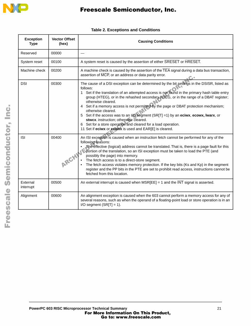
The 603’s exceptions, and conditions that cause them, are listed in Table 2. Exceptions that are specific tothe 603 are indicated.
Table 1. PowerPC 603 Microprocessor Exception Classifications
Synchronous/Asynchronous Precise/Imprecise Exception Type
Asynchronous, nonmaskable Imprecise Machine checkSystem reset
Asynchronous, maskable Precise External interruptDecrementerSystem management interrupt
Synchronous Precise Instruction-caused exceptions
ARCHIVED BY FREESCALE SEMICONDUCTOR, INC.
20 PowerPC 603 RISC Microprocessor Technical Summary For More Information On This Product,
Go to: www.freescale.com
E
Res
Sys
Mac n,
DSI s
ry r;
ISI
is
t be
Extinte
Alig of an
F
ree
sca
le S
em
ico
nd
uc
tor,
I
Freescale Semiconductor, Inc.n
c..
.
Table 2. Exceptions and Conditions
xception Type
Vector Offset(hex)
Causing Conditions
erved 00000 —
tem reset 00100 A system reset is caused by the assertion of either SRESET or HRESET.
hine check 00200 A machine check is caused by the assertion of the TEA signal during a data bus transactioassertion of MCP, or an address or data parity error.
00300 The cause of a DSI exception can be determined by the bit settings in the DSISR, listed afollows:1 Set if the translation of an attempted access is not found in the primary hash table ent
group (HTEG), or in the rehashed secondary HTEG, or in the range of a DBAT registeotherwise cleared.
4 Set if a memory access is not permitted by the page or DBAT protection mechanism; otherwise cleared.
5 Set if the access was to an I/O segment (SR[T] =1) by an eciwx, ecowx, lwarx, or stwcx. instruction; otherwise cleared.
6 Set for a store operation and cleared for a load operation. 11 Set if eciwx or ecowx is used and EAR[E] is cleared.
00400 An ISI exception is caused when an instruction fetch cannot be performed for any of the following reasons:• The effective (logical) address cannot be translated. That is, there is a page fault for th
portion of the translation, so an ISI exception must be taken to load the PTE (and possibly the page) into memory.
• The fetch access is to a direct-store segment.• The fetch access violates memory protection. If the key bits (Ks and Kp) in the segmen
register and the PP bits in the PTE are set to prohibit read access, instructions cannot fetched from this location.
ernal rrupt
00500 An external interrupt is caused when MSR[EE] = 1 and the INT signal is asserted.
nment 00600 An alignment exception is caused when the 603 cannot perform a memory access for anyseveral reasons, such as when the operand of a floating-point load or store operation is in I/O segment (SR[T] = 1).
ARCHIVED BY FREESCALE SEMICONDUCTOR, INC.
PowerPC 603 RISC Microprocessor Technical Summary 21 For More Information On This Product,
Go to: www.freescale.com
Pro
ed n R. n
nd or o
r
d
Floauna
Dec )
Res
Sys
Trac is
Res se
Res
Insttranmis
Dattranmis
d
Dattranmis
re bit
Instaddbre
le
E
F
ree
sca
le S
em
ico
nd
uc
tor,
I
Freescale Semiconductor, Inc.n
c..
.
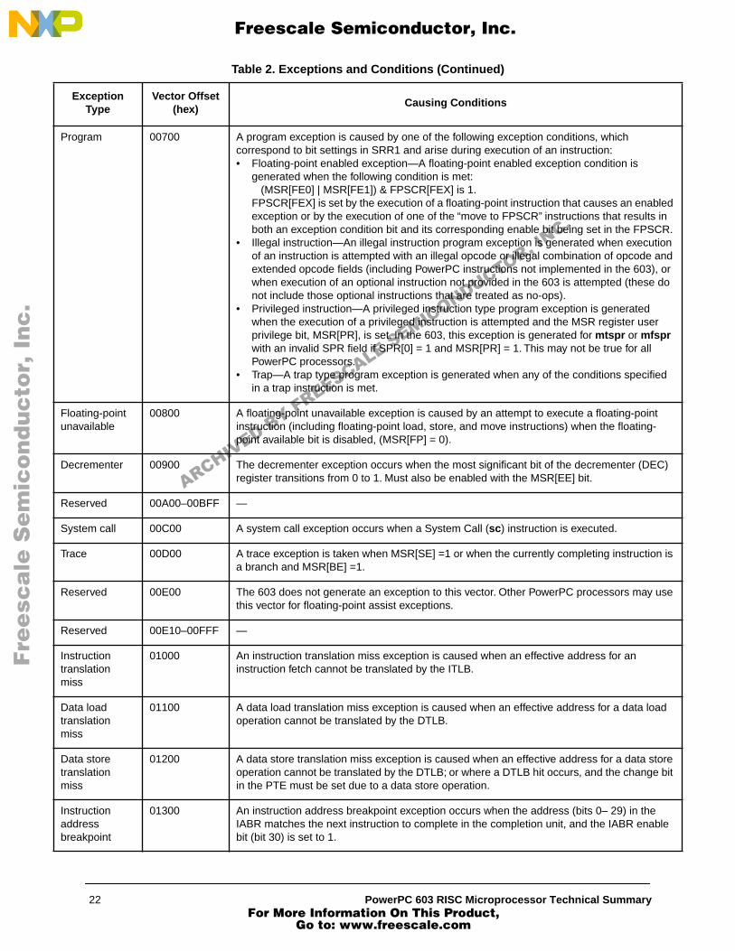
gram 00700 A program exception is caused by one of the following exception conditions, which correspond to bit settings in SRR1 and arise during execution of an instruction:• Floating-point enabled exception—A floating-point enabled exception condition is
generated when the following condition is met: (MSR[FE0] | MSR[FE1]) & FPSCR[FEX] is 1.
FPSCR[FEX] is set by the execution of a floating-point instruction that causes an enablexception or by the execution of one of the “move to FPSCR” instructions that results iboth an exception condition bit and its corresponding enable bit being set in the FPSC
• Illegal instruction—An illegal instruction program exception is generated when executioof an instruction is attempted with an illegal opcode or illegal combination of opcode aextended opcode fields (including PowerPC instructions not implemented in the 603), when execution of an optional instruction not provided in the 603 is attempted (these dnot include those optional instructions that are treated as no-ops).
• Privileged instruction—A privileged instruction type program exception is generated when the execution of a privileged instruction is attempted and the MSR register user privilege bit, MSR[PR], is set. In the 603, this exception is generated for mtspr or mfspwith an invalid SPR field if SPR[0] = 1 and MSR[PR] = 1. This may not be true for all PowerPC processors.
• Trap—A trap type program exception is generated when any of the conditions specifiein a trap instruction is met.
ting-point vailable
00800 A floating-point unavailable exception is caused by an attempt to execute a floating-point instruction (including floating-point load, store, and move instructions) when the floating-point available bit is disabled, (MSR[FP] = 0).
rementer 00900 The decrementer exception occurs when the most significant bit of the decrementer (DECregister transitions from 0 to 1. Must also be enabled with the MSR[EE] bit.
erved 00A00–00BFF —
tem call 00C00 A system call exception occurs when a System Call (sc) instruction is executed.
e 00D00 A trace exception is taken when MSR[SE] =1 or when the currently completing instructiona branch and MSR[BE] =1.
erved 00E00 The 603 does not generate an exception to this vector. Other PowerPC processors may uthis vector for floating-point assist exceptions.
erved 00E10–00FFF —
ruction slation s
01000 An instruction translation miss exception is caused when an effective address for an instruction fetch cannot be translated by the ITLB.
a load slation s
01100 A data load translation miss exception is caused when an effective address for a data loaoperation cannot be translated by the DTLB.
a store slation s
01200 A data store translation miss exception is caused when an effective address for a data stooperation cannot be translated by the DTLB; or where a DTLB hit occurs, and the change in the PTE must be set due to a data store operation.
ruction ress akpoint
01300 An instruction address breakpoint exception occurs when the address (bits 0– 29) in the IABR matches the next instruction to complete in the completion unit, and the IABR enabbit (bit 30) is set to 1.
Table 2. Exceptions and Conditions (Continued)
xception Type
Vector Offset(hex)
Causing Conditions
ARCHIVED BY FREESCALE SEMICONDUCTOR, INC.
22 PowerPC 603 RISC Microprocessor Technical Summary For More Information On This Product,
Go to: www.freescale.com
Sysmaninte
Res
E
F
ree
sca
le S
em
ico
nd
uc
tor,
I
Freescale Semiconductor, Inc.n
c..
.
3.6 Memory ManagementThe following subsections describe the memory management features of the PowerPC architecture, and the603 implementation, respectively.
3.6.1 PowerPC Memory ManagementThe primary functions of the MMU are to translate logical (effective) addresses to physical addresses formemory accesses, I/O accesses (most I/O accesses are assumed to be memory-mapped), and direct-storeinterface accesses, and to provide access protection on blocks and pages of memory.
There are three types of accesses generated by the 603 that require address translation— instructionaccesses, data accesses to memory generated by load and store instructions, and direct-store interfaceaccesses generated by load and store instructions.
The PowerPC MMU and exception model support demand-paged virtual memory. Virtual memorymanagement permits execution of programs larger than the size of physical memory; demand-paged impliesthat individual pages are loaded into physical memory from system memory only when they are firstaccessed by an executing program.
The hashed page table is a variable-sized data structure that defines the mapping between virtual pagenumbers and physical page numbers. The page table size is a power of 2, and its starting address is a multipleof its size.
The page table contains a number of page table entry groups (PTEGs). A PTEG contains eight page tableentries (PTEs) of eight bytes each; therefore, each PTEG is 64 bytes long. PTEG addresses are entry pointsfor table search operations.
Address translations are enabled by setting bits in the MSR—MSR[IR] enables instruction addresstranslations and MSR[DR] enables data address translations.
3.6.2 PowerPC 603 Microprocessor Memory ManagementThe instruction and data memory management units in the 603 provide 4 Gbytes of logical address spaceaccessible to supervisor and user programs with a 4-Kbyte page size and 256-Mbyte segment size. Blocksizes range from 128 Kbyte to 256 Mbyte and are software selectable. In addition, the 603 uses an interim52-bit virtual address and hashed page tables for generating 32-bit physical addresses. The MMUs in the603 rely on the exception processing mechanism for the implementation of the paged virtual memoryenvironment and for enforcing protection of designated memory areas.
Instruction and data TLBs provide address translation in parallel with the on-chip cache access, incurringno additional time penalty in the event of a TLB hit. A TLB is a cache of the most recently used page tableentries. Software is responsible for maintaining the consistency of the TLB with memory. The 603’s TLBsare 64-entry, two-way set-associative caches that contain instruction and data address translations. The 603provides hardware assist for software table search operations through the hashed page table on TLB misses.Supervisor software can invalidate TLB entries selectively.
tem agement
rrupt
01400 A system management interrupt is caused when MSR[EE] =1 and the SMI input signal isasserted.
erved 01500–02FFF —
Table 2. Exceptions and Conditions (Continued)
xception Type
Vector Offset(hex)
Causing Conditions
ARCHIVED BY FREESCALE SEMICONDUCTOR, INC.
PowerPC 603 RISC Microprocessor Technical Summary 23 For More Information On This Product,
Go to: www.freescale.com
F
ree
sca
le S
em
ico
nd
uc
tor,
I
Freescale Semiconductor, Inc.n
c..
.
The 603 also provides independent four-entry BAT arrays for instructions and data that maintain addresstranslations for blocks of memory. These entries define blocks that can vary from 128 Kbytes to 256 Mbytes.The BAT arrays are maintained by system software.
As specified by the PowerPC architecture, the hashed page table is a variable-sized data structure thatdefines the mapping between virtual page numbers and physical page numbers. The page table size is apower of 2, and its starting address is a multiple of its size.
Also as specified by the PowerPC architecture, the page table contains a number of page table entry groups(PTEGs). A PTEG contains eight page table entries (PTEs) of eight bytes each; therefore, each PTEG is 64bytes long. PTEG addresses are entry points for table search operations.
3.7 Instruction TimingThe 603 is a pipelined superscalar processor. A pipelined processor is one in which the processing of aninstruction is reduced into discrete stages. Because the processing of an instruction is broken into a seriesof stages, an instruction does not require the entire resources of an execution unit. For example, after aninstruction completes the decode stage, it can pass on to the next stage, while the subsequent instruction canadvance into the decode stage. This improves the throughput of the instruction flow. For example, it maytake three cycles for a floating-point instruction to complete, but if there are no stalls in the floating-pointpipeline, a series of floating-point instructions can have a throughput of one instruction per cycle.
The instruction pipeline in the 603 has four major pipeline stages, described as follows:
• The fetch pipeline stage primarily involves retrieving instructions from the memory system and determining the location of the next instruction fetch. Additionally, the BPU decodes branches during the fetch stage and folds out branch instructions before the dispatch stage if possible.
• The dispatch pipeline stage is responsible for decoding the instructions supplied by the instruction fetch stage, and determining which of the instructions are eligible to be dispatched in the current cycle. In addition, the source operands of the instructions are read from the appropriate register file and dispatched with the instruction to the execute pipeline stage. At the end of the dispatch pipeline stage, the dispatched instructions and their operands are latched by the appropriate execution unit.
• During the execute pipeline stage each execution unit that has an executable instruction executes the selected instruction (perhaps over multiple cycles), writes the instruction's result into the appropriate rename register, and notifies the completion stage that the instruction has finished execution. In the case of an internal exception, the execution unit reports the exception to the completion/writeback pipeline stage and discontinues instruction execution until the exception is handled. The exception is not signaled until that instruction is the next to be completed. Execution of most floating-point instructions is pipelined within the FPU allowing up to three instructions to be executing in the FPU concurrently. The pipeline stages for the floating-point unit are multiply, add, and round-convert. Execution of most load/store instructions is also pipelined. The load/store unit has two pipeline stages. The first stage is for effective address calculation and MMU translation and the second stage is for accessing the data in the cache.
• The complete/writeback pipeline stage maintains the correct architectural machine state and transfers the contents of the rename registers to the GPRs and FPRs as instructions are retired. If the completion logic detects an instruction causing an exception, all following instructions are cancelled, their execution results in rename registers are discarded, and instructions are fetched from the correct instruction stream.
A superscalar processor is one that issues multiple independent instructions into multiple pipelines allowinginstructions to execute in parallel. The 603 has five independent execution units, one each for integerinstructions, floating-point instructions, branch instructions, load/store instructions, and system registerinstructions. The IU and the FPU each have dedicated register files for maintaining operands (GPRs and
ARCHIVED BY FREESCALE SEMICONDUCTOR, INC.
24 PowerPC 603 RISC Microprocessor Technical Summary For More Information On This Product,
Go to: www.freescale.com
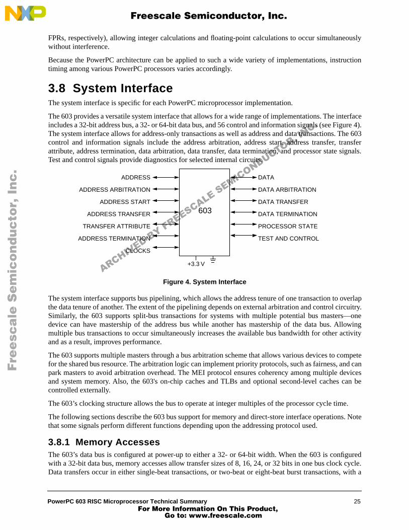
F
ree
sca
le S
em
ico
nd
uc
tor,
I
Freescale Semiconductor, Inc.n
c..
.
FPRs, respectively), allowing integer calculations and floating-point calculations to occur simultaneouslywithout interference.
Because the PowerPC architecture can be applied to such a wide variety of implementations, instructiontiming among various PowerPC processors varies accordingly.
3.8 System Interface The system interface is specific for each PowerPC microprocessor implementation.
The 603 provides a versatile system interface that allows for a wide range of implementations. The interfaceincludes a 32-bit address bus, a 32- or 64-bit data bus, and 56 control and information signals (see Figure 4).The system interface allows for address-only transactions as well as address and data transactions. The 603control and information signals include the address arbitration, address start, address transfer, transferattribute, address termination, data arbitration, data transfer, data termination, and processor state signals.Test and control signals provide diagnostics for selected internal circuits.
Figure 4. System Interface
The system interface supports bus pipelining, which allows the address tenure of one transaction to overlapthe data tenure of another. The extent of the pipelining depends on external arbitration and control circuitry.Similarly, the 603 supports split-bus transactions for systems with multiple potential bus masters—onedevice can have mastership of the address bus while another has mastership of the data bus. Allowingmultiple bus transactions to occur simultaneously increases the available bus bandwidth for other activityand as a result, improves performance.
The 603 supports multiple masters through a bus arbitration scheme that allows various devices to competefor the shared bus resource. The arbitration logic can implement priority protocols, such as fairness, and canpark masters to avoid arbitration overhead. The MEI protocol ensures coherency among multiple devicesand system memory. Also, the 603's on-chip caches and TLBs and optional second-level caches can becontrolled externally.
The 603’s clocking structure allows the bus to operate at integer multiples of the processor cycle time.
The following sections describe the 603 bus support for memory and direct-store interface operations. Notethat some signals perform different functions depending upon the addressing protocol used.
3.8.1 Memory AccessesThe 603’s data bus is configured at power-up to either a 32- or 64-bit width. When the 603 is configuredwith a 32-bit data bus, memory accesses allow transfer sizes of 8, 16, 24, or 32 bits in one bus clock cycle.Data transfers occur in either single-beat transactions, or two-beat or eight-beat burst transactions, with a
603
ADDRESS
ADDRESS ARBITRATION
ADDRESS START
ADDRESS TRANSFER
TRANSFER ATTRIBUTE
ADDRESS TERMINATION
CLOCKS
DATA
DATA ARBITRATION
DATA TRANSFER
DATA TERMINATION
PROCESSOR STATE
TEST AND CONTROL
+3.3 VARCHIVED BY FREESCALE SEMICONDUCTOR, INC.
PowerPC 603 RISC Microprocessor Technical Summary 25 For More Information On This Product,
Go to: www.freescale.com
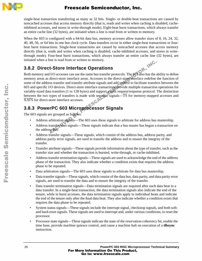
F
ree
sca
le S
em
ico
nd
uc
tor,
I
Freescale Semiconductor, Inc.n
c..
.
single-beat transaction transferring as many as 32 bits. Single- or double-beat transactions are caused bynoncached accesses that access memory directly (that is, reads and writes when caching is disabled, cache-inhibited accesses, and stores in write-through mode). Eight-beat burst transactions, which always transferan entire cache line (32 bytes), are initiated when a line is read from or written to memory.
When the 603 is configured with a 64-bit data bus, memory accesses allow transfer sizes of 8, 16, 24, 32,40, 48, 56, or 64 bits in one bus clock cycle. Data transfers occur in either single-beat transactions or four-beat burst transactions. Single-beat transactions are caused by noncached accesses that access memorydirectly (that is, reads and writes when caching is disabled, cache-inhibited accesses, and stores in write-through mode). Four-beat burst transactions, which always transfer an entire cache line (32 bytes), areinitiated when a line is read from or written to memory.
3.8.2 Direct-Store Interface OperationsBoth memory and I/O accesses can use the same bus transfer protocols. The 603 also has the ability to definememory areas as direct-store interface areas. Accesses to the direct-store interface redefine the function ofsome of the address transfer and transfer attribute signals and add control to facilitate transfers between the603 and specific I/O devices. Direct-store interface transactions provide multiple transaction operations forvariably-sized data transfers (1 to 128 bytes) and support a split request/response protocol. The distinctionbetween the two types of transfers is made with separate signals—TS for memory-mapped accesses andXATS for direct-store interface accesses.
3.8.3 PowerPC 603 Microprocessor SignalsThe 603 signals are grouped as follows:
• Address arbitration signals—The 603 uses these signals to arbitrate for address bus mastership.
• Address transfer start signals—These signals indicate that a bus master has begun a transaction on the address bus.
• Address transfer signals—These signals, which consist of the address bus, address parity, and address parity error signals, are used to transfer the address and to ensure the integrity of the transfer.
• Transfer attribute signals—These signals provide information about the type of transfer, such as the transfer size and whether the transaction is bursted, write-through, or cache-inhibited.
• Address transfer termination signals—These signals are used to acknowledge the end of the address phase of the transaction. They also indicate whether a condition exists that requires the address phase to be repeated.
• Data arbitration signals—The 603 uses these signals to arbitrate for data bus mastership.
• Data transfer signals—These signals, which consist of the data bus, data parity, and data parity error signals, are used to transfer the data and to ensure the integrity of the transfer.
• Data transfer termination signals—Data termination signals are required after each data beat in a data transfer. In a single-beat transaction, the data termination signals also indicate the end of the tenure, while in burst accesses, the data termination signals apply to individual beats and indicate the end of the tenure only after the final data beat. They also indicate whether a condition exists that requires the data phase to be repeated.
• System status signals—These signals include the interrupt signal, checkstop signals, and both soft- and hard-reset signals. These signals are used to interrupt and, under various conditions, to reset the processor.
• Processor state signals—These signals indicate the state of the reservation coherency bit, enable the time base, provide machine quiesce control, and cause a machine halt on execution of a tlbsync instruction.
ARCHIVED BY FREESCALE SEMICONDUCTOR, INC.
26 PowerPC 603 RISC Microprocessor Technical Summary For More Information On This Product,
Go to: www.freescale.com
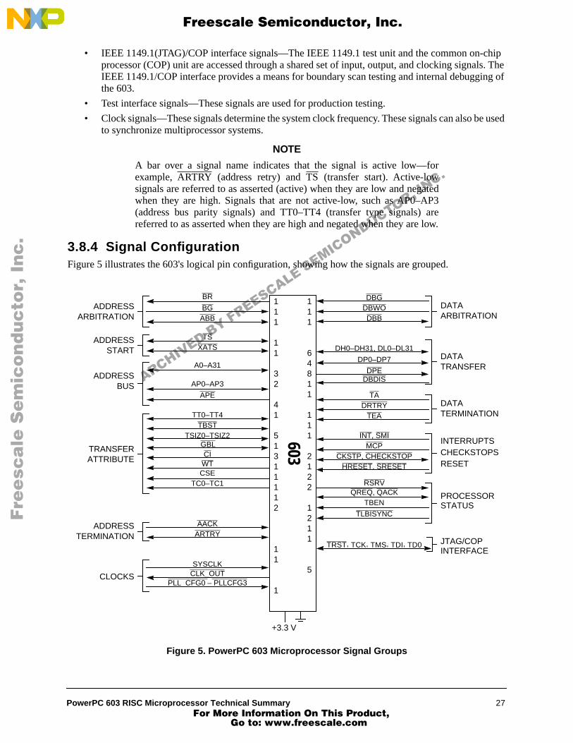
F
ree
sca
le S
em
ico
nd
uc
tor,
I
Freescale Semiconductor, Inc.n
c..
.
• IEEE 1149.1(JTAG)/COP interface signals—The IEEE 1149.1 test unit and the common on-chip processor (COP) unit are accessed through a shared set of input, output, and clocking signals. The IEEE 1149.1/COP interface provides a means for boundary scan testing and internal debugging of the 603.
• Test interface signals—These signals are used for production testing.
• Clock signals—These signals determine the system clock frequency. These signals can also be used to synchronize multiprocessor systems.
NOTE
A bar over a signal name indicates that the signal is active low—forexample, ARTRY (address retry) and TS (transfer start). Active-lowsignals are referred to as asserted (active) when they are low and negatedwhen they are high. Signals that are not active-low, such as AP0–AP3(address bus parity signals) and TT0–TT4 (transfer type signals) arereferred to as asserted when they are high and negated when they are low.
3.8.4 Signal ConfigurationFigure 5 illustrates the 603's logical pin configuration, showing how the signals are grouped.
Figure 5. PowerPC 603 Microprocessor Signal Groups
111
11
32
41
51311112
11
1
111
64811
111
2122
1211
5
603DBG
DBWODBB
DH0–DH31, DL0–DL31
DP0–DP7
DPEDBDIS
TADRTRY
TEA
INT, SMIMCP
CKSTP, CHECKSTOPHRESET, SRESET
RSRVQREQ, QACK
TBEN
TLBISYNC
TRST, TCK, TMS, TDI, TD0
ADDRESSARBITRATION
ADDRESSSTART
ADDRESSBUS
TRANSFERATTRIBUTE
ADDRESSTERMINATION
CLOCKS
DATAARBITRATION
DATATRANSFER
DATATERMINATION
INTERRUPTSCHECKSTOPSRESET
PROCESSORSTATUS
JTAG/COPINTERFACE
+3.3 V
GBL
BR
BGABB
TSXATS
A0–A31
AP0–AP3
APE
TT0–TT4TBST
TSIZ0–TSIZ2
CIWTCSE
TC0–TC1
AACKARTRY
SYSCLKCLK_OUT
PLL_CFG0 – PLLCFG3
ARCHIVED BY FREESCALE SEMICONDUCTOR, INC.
PowerPC 603 RISC Microprocessor Technical Summary 27 For More Information On This Product,
Go to: www.freescale.com
F
ree
sca
le S
em
ico
nd
uc
tor,
IFreescale Semiconductor, Inc.
nc
...
ICONDUCTOR, INC.
Information in this document is provided solely to enable system and software implementers to use PowerPC microprocessors. There are no express or impliedcopyright licenses granted hereunder to design or fabricate PowerPC integrated circuits or integrated circuits based on the information in this document.
The PowerPC 603 microprocessor embodies the intellectual property of IBM and of Motorola. However, neither party assumes any responsibility or liability as toany aspects of the performance, operation, or other attributes of the microprocessor as marketed by the other party. Neither party is to be considered an agent orrepresentative of the other party, and neither has granted any right or authority to the other to assume or create any express or implied obligations on its behalf.Information such as errata sheets and data sheets, as well as sales terms and conditions such as prices, schedules, and support, for the microprocessor may varyas between IBM and Motorola. Accordingly, customers wishing to learn more information about the products as marketed by a given party should contact that party.
Both IBM and Motorola reserve the right to modify this manual and/or any of the products as described herein without further notice. Nothing in this manual, norin any of the errata sheets, data sheets, and other supporting documentation, shall be interpreted as conveying an express or implied warranty, representation, orguarantee regarding the suitability of the products for any particular purpose. The parties do not assume any liability or obligation for damages of any kind arisingout of the application or use of these materials. Any warranty or other obligations as to the products described herein shall be undertaken solely by the marketingparty to the customer, under a separate sale agreement between the marketing party and the customer. In the absence of such an agreement, no liability isassumed by the marketing party for any damages, actual or otherwise.
“Typical” parameters can and do vary in different applications. All operating parameters, including “Typicals,” must be validated for each customer application bycustomer’s technical experts. Neither IBM nor Motorola convey any license under their respective intellectual property rights nor the rights of others. The productsdescribed in this manual are not designed, intended, or authorized for use as components in systems intended for surgical implant into the body, or otherapplications intended to support or sustain life, or for any other application in which the failure of the product could create a situation where personal injury or deathmay occur. Should customer purchase or use the products for any such unintended or unauthorized application, customer shall indemnify and hold IBM andMotorola and their respective officers, employees, subsidiaries, affiliates, and distributors harmless against all claims, costs, damages, and expenses, andreasonable attorney fees arising out of, directly or indirectly, any claim of personal injury or death associated with such unintended or unauthorized use, even ifsuch claim alleges that Motorola or IBM was negligent regarding the design or manufacture of the part.
Motorola and are registered trademarks of Motorola, Inc. Motorola, Inc. is an Equal Opportunity/Affirmative Action Employer.
IBM is a registered trademark of IBM Corp. , , PowerPC, PowerPC Architecture, POWER Architecture, PowerPC 603,and PowerPC 601 are trademarks of International Business Machines Corp. used by Motorola under license from IBM Corp.
Motorola Literature Distribution Centers:USA: Motorola Literature Distribution, P.O. Box 20912, Phoenix, Arizona 85036.EUROPE: Motorola Ltd., European Literature Centre, 88 Tanners Drive, Blakelands, Milton Keynes, MK14 5BP, England.JAPAN: Nippon Motorola Ltd., 4-32-1, Nishi-Gotanda, Shinagawa-ku, Tokyo 141 Japan.ASIA-PACIFIC: Motorola Semiconductors H.K. Ltd., Silicon Harbour Centre, No. 2 Dai King Street, Tai Po Industrial Estate,Tai Po, N.T., Hong Kong.Technical Information: Motorola Inc. Semiconductor Products Sector Technical Responsiveness Center; (800) 521-6274.Document Comments: FAX (512) 891-2638, Attn: RISC Applications Engineering.
IBM Microelectronics:USA: IBM Microelectronics, Mail Stop A25/862-1, PowerPC Marketing, 1000 River Street, Essex Junction, VT 05452-4299; Tel.: (800) PowerPC [(800) 769-3772]; FAX (800) POWERfax [(800) 769-3732].EUROPE: IBM Microelectronics, PowerPC Marketing, Dept. 1045, 224 Boulevard J.F. Kennedy, 91105 Corbeil-EssonnesCEDEX, France; Tel. (33) 1-60-88 5167; FAX (33) 1-60-88 4920.JAPAN: IBM Microelectronics, PowerPC Marketing, Dept., R0260, 800 Ichimiyake, Yasu-cho, Yasu-gun, Shinga-ken, Japan520-23; Tel. (81) 775-87-4745; FAX (81) 775-87-4735.
For More Information On This Product, Go to: www.freescale.com
ARCHIVED BY FREESCALE SEM