Embed Size (px)
Citation preview
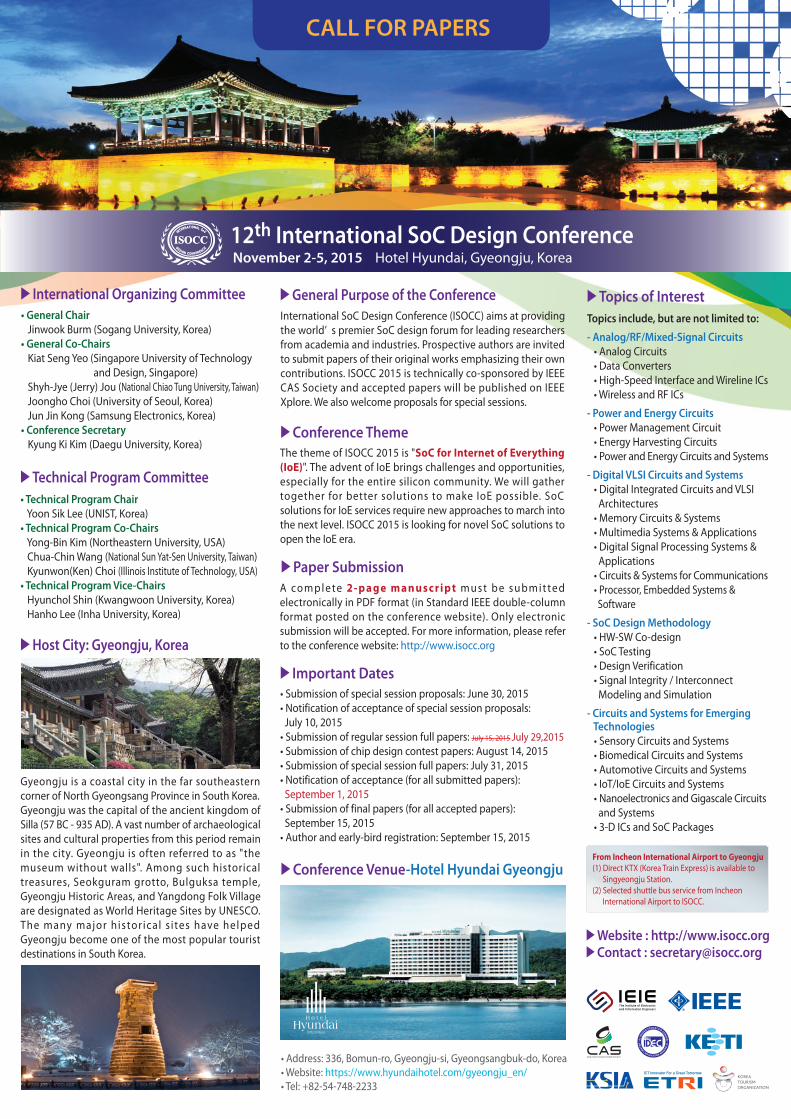
November 2-5, 2015 Hotel Hyundai, Gyeongju, Korea
▶Website : http://www.isocc.org▶Contact : [email protected]
Topics include, but are not limited to:
- Analog/RF/Mixed-Signal Circuits • Analog Circuits • Data Converters • High-Speed Interface and Wireline ICs • Wireless and RF ICs
- Power and Energy Circuits • Power Management Circuit • Energy Harvesting Circuits • Power and Energy Circuits and Systems
- Digital VLSI Circuits and Systems • Digital Integrated Circuits and VLSI Architectures • Memory Circuits & Systems • Multimedia Systems & Applications • Digital Signal Processing Systems & Applications • Circuits & Systems for Communications • Processor, Embedded Systems & Software
- SoC Design Methodology • HW-SW Co-design • SoC Testing • Design Verification • Signal Integrity / Interconnect Modeling and Simulation
- Circuits and Systems for Emerging Technologies • Sensory Circuits and Systems • Biomedical Circuits and Systems • Automotive Circuits and Systems • IoT/IoE Circuits and Systems • Nanoelectronics and Gigascale Circuits and Systems • 3-D ICs and SoC Packages
▶Topics of Interest▶General Purpose of the Conference
CALL FOR PAPERS
International SoC Design Conference (ISOCC) aims at providing the world’ s premier SoC design forum for leading researchers from academia and industries. Prospective authors are invited to submit papers of their original works emphasizing their own contributions. ISOCC 2015 is technically co-sponsored by IEEE CAS Society and accepted papers will be published on IEEE Xplore. We also welcome proposals for special sessions.
▶Conference ThemeThe theme of ISOCC 2015 is "SoC for Internet of Everything (IoE)". The advent of IoE brings challenges and opportunities, especially for the entire silicon community. We will gather together for better solutions to make IoE possible. SoC solutions for IoE services require new approaches to march into the next level. ISOCC 2015 is looking for novel SoC solutions to open the IoE era.
▶Paper SubmissionA co m p l e te 2 - p a g e m a n u s c r i p t m u s t b e s u b m i t te d electronically in PDF format (in Standard IEEE double-column format posted on the conference website). Only electronic submission will be accepted. For more information, please refer to the conference website: http://www.isocc.org
▶Important Dates
▶Conference Venue-Hotel Hyundai Gyeongju
• Submission of special session proposals: June 30, 2015• Notification of acceptance of special session proposals: July 10, 2015• Submission of regular session full papers: July 15, 2015 July 29,2015• Submission of chip design contest papers: August 14, 2015• Submission of special session full papers: July 31, 2015• Notification of acceptance (for all submitted papers): September 1, 2015• Submission of final papers (for all accepted papers): September 15, 2015• Author and early-bird registration: September 15, 2015
• Address: 336, Bomun-ro, Gyeongju-si, Gyeongsangbuk-do, Korea• Website: https://www.hyundaihotel.com/gyeongju_en/• Tel: +82-54-748-2233
From Incheon International Airport to Gyeongju(1) Direct KTX (Korea Train Express) is available to Singyeongju Station.(2) Selected shuttle bus service from Incheon International Airport to ISOCC.
12th International SoC Design Conference
▶International Organizing Committee
• Technical Program Chair Yoon Sik Lee (UNIST, Korea)• Technical Program Co-Chairs Yong-Bin Kim (Northeastern University, USA) Chua-Chin Wang (National Sun Yat-Sen University, Taiwan) Kyunwon(Ken) Choi (Illinois Institute of Technology, USA)• Technical Program Vice-Chairs Hyunchol Shin (Kwangwoon University, Korea) Hanho Lee (Inha University, Korea)
▶Technical Program Committee
▶Host City: Gyeongju, Korea
Gyeongju is a coastal city in the far southeastern corner of North Gyeongsang Province in South Korea. Gyeongju was the capital of the ancient kingdom of Silla (57 BC - 935 AD). A vast number of archaeological sites and cultural properties from this period remain in the city. Gyeongju is often referred to as "the museum without walls". Among such historical treasures, Seokguram grotto, Bulguksa temple, Gyeongju Historic Areas, and Yangdong Folk Village are designated as World Heritage Sites by UNESCO. The many major histor ical s i tes have helped Gyeongju become one of the most popular tourist destinations in South Korea.
• General Chair Jinwook Burm (Sogang University, Korea)• General Co-Chairs Kiat Seng Yeo (Singapore University of Technology and Design, Singapore) Shyh-Jye (Jerry) Jou (National Chiao Tung University, Taiwan) Joongho Choi (University of Seoul, Korea) Jun Jin Kong (Samsung Electronics, Korea)• Conference Secretary Kyung Ki Kim (Daegu University, Korea)
10 International SoC Design Conference
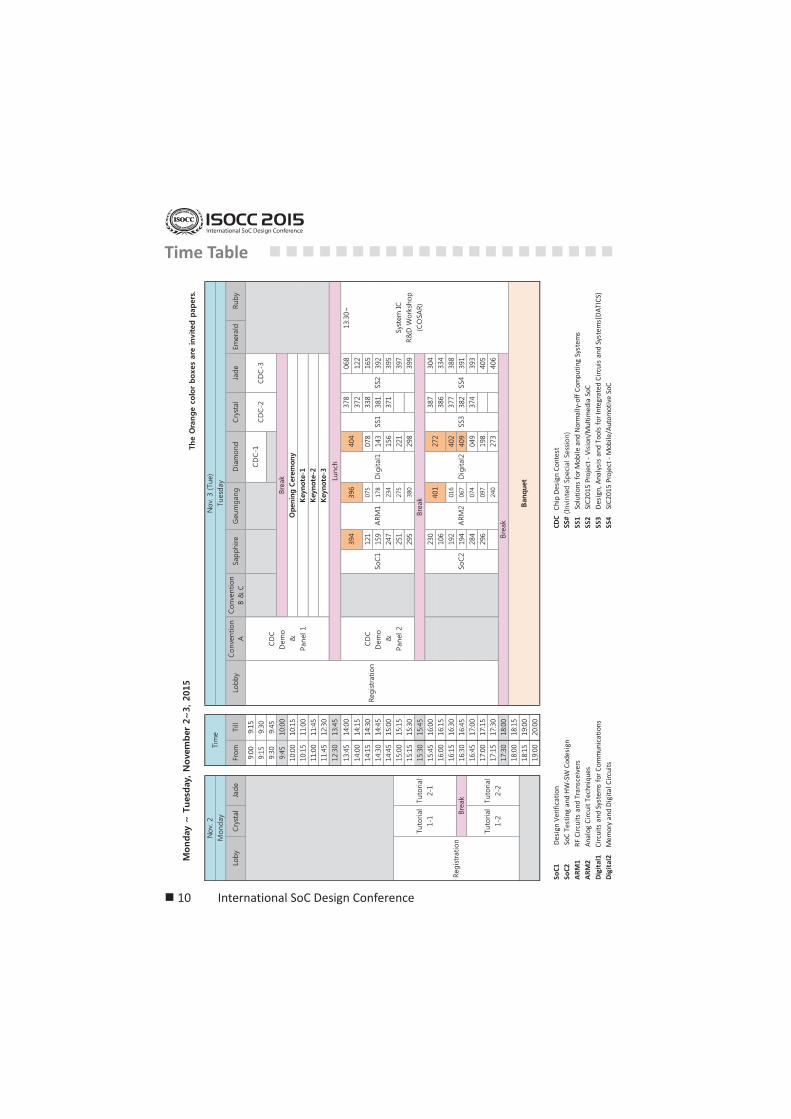
Time Table
SoC1
D
esig
n Ve
rific
atio
nCD
C C
hip
Desi
gn C
onte
stSo
C2
SoC
Tes
ting
and
HW-S
W C
odes
ign
ARM
1
RF
Circ
uits
and
Tra
nsce
iver
sSS
1
Solu
tions
for M
obile
and
Nor
mal
ly-o
ff Co
mpu
ting
Syst
ems
ARM
2
An
alog
Circ
uit T
echn
ique
sSS
2
SIC2
015
Proj
ect -
Vis
ion/
Mul
timed
ia S
oCDi
gita
l1
Circ
uits
and
Sys
tem
s fo
r Com
mun
icat
ions
SS3
De
sign
, Ana
lysi
s an
d To
ols
for I
nteg
rate
d Ci
rcui
s an
d Sy
stem
s(DA
TICS
)Di
gita
l2
Mem
ory
and
Digi
tal C
ircui
tsSS
4
SIC2
015
Proj
ect -
Mob
ile/A
utom
otiv
e So
C
Anrtisu Session RF Circuits and Transceivers Nov. 3, 13:45~15:30 Geumgang
Chair: Kang-Yoon Lee (Sungkyunkwan University, Korea)
Invited Paper RF Receiver Design for IOE Applications Joung Won Park Qualcomm Technology Inc., USA.
A Low-Voltage PLL with a Current Mismatch Compensated Charge Pump Sung-Geun Kim, Jinsoo Rhim, Dae-Hyun Kwon, Min-Hyeong Kim, and Woo-Young Choi Yonsei University, Korea
A 10 Gbps SerDes For Wireless Chip-to-chip Communication Sangwoo Han1, Taegyu Kim1, Jintae Kim2, and Jongsun Kim1 1Hongik University, Korea 2Konkuk University, Korea
A design of META-VCO based-on meta-material using CMOS process Jongsuk Lee and Yong Moon Soongsil University, Korea
A Low Power RF CMOS Direct-Conversion Transmitter Using High Conversion Gain Front end for IEEE 802.15.4 Standard Changwon Seo1,2, Hanjin Cho1, Seyoung Baik2 , Jinyong Kim2 , Ho Jeong Jin2, and Choon Sik Cho2 1ETRI, Korea 2Korea Aerospace University, Korea
Design of a 40GHz PLL Frequency Synthesizer with Wide Locking Range ILFD in 65nm CMOS Woongtae Nam, Jihoon Son, and Hyunchol Shin Kwangwoon University,Korea

-1- ISOCC 2015
A Low-Voltage PLL with a Current Mismatch Compensated Charge Pump
Sung-Geun Kim, Jinsoo Rhim, Dae-Hyun Kwon, Min-Hyeong Kim, and Woo-Young Choi Department of Electrical and Electronic Engineering, Yonsei University
Seodaemun-gu, Seoul 120-749, Korea [email protected]
Abstract—A low-voltage phase-locked loop (PLL) circuit having a charge pump (CP) with a novel negative feedback replica bias scheme for current mismatch compensation is demonstrated. A prototype 400-MHz PLL circuit operating at 0.65-V is fabricated with 180-nm standard CMOS process. Measurement results show that current mismatch compensation is successfully achieved. Our PLL consumes only 140-μW.
Keywords-component;low voltage charge pump, phase locked loop, power efficiency, spur reduction
I. INTRODUCTION
Power consumption reduction is the key design consi-deration for modern integrated circuits. Lowering the supply voltage is the most effective way for achieving this goal and optimal design of mixed-signal circuits such as phase-locked loops (PLLs) operating at low supply voltages is attracting research interests [1]-[3].
With low supply voltages, transistors used for current sources become more sensitive to drain-to-source voltage (VDS) variations. This can be a serious problem for the charge pump (CP) in PLL as it results in the reference spur due to CP current mismatch. Several design techniques for preventing this problem have been reported [2, 3]. In [2], dynamic-threshold CMOS is used to alleviate the voltage headroom problem but this requires special processing technology. An active loop-filter (ALF) with a single-ended two-stacked CP is used in [3], but this can suffer from inferior noise performance due to active devices in the loop-filter. Moreover, designing OP-amp used in ALF can be challenging for low supply-voltage applications.
In this paper, we present a low-voltage PLL with a novel structure for current mismatch compensating charge pump. Our PLL realized in 180-nm CMOS achieves 400-MHz operation at 0.65-V supply voltage with well-compensated CP current mismatch.
II. CIRCUIT IMPLEMENTATION
A. PLL Architecture
Fig. 1 shows the block diagram of our PLL. The CP has a two-transistor stacked gate-controlled structure and the phase-frequency detector (PFD) consists of conventional CMOS logic
gates and D-flip flops (DFFs). The VCO has inverter based pseudo differential structure. The divide-by-16 frequency divider consists of an extended true-single-phase-clock (E-TSPC) DFF and three TSPC DFFs [4].
B. Charge Pump
The structure of our CP with a novel negative feedback replica bias circuit is shown in Fig. 2. The CP structure is based on two-stack gate-controlled CP for low supply-voltage operation [1]. The conventional replica bias circuit uses negative feedback by directly connecting OP-amp output to the switching node for current mismatch compensation [5]. However, this requires high slew-rate OP-amp for fast switching operating, which can consume a significant amount of power and optimal design of which can be challenging for low supply-voltage applications. In our CP, the negative feedback bias is divided into replica circuit and VBiasP generator
This work was supported by the National Research Foundation of Korea (NRF) grant funded by the Korea government (MEST) [2015R1A2A2A01007772]. The authors are thankful to IC Design Education Center (IDEC) for EDA software and MPW support.
Figure 2. Two-stack gate-controlled CP with a bias circuit.
Figure 1. PLL block diagram.

-2- ISOCC 2015
to avoid direct connection between OP-amp output and the switching node, VBiasP. The output of OP-amp (VMis) controls the gate node of MNBias and generates proper VBiasP, which makes the voltage of FBCP same as same as that of OUTCP. The VBiasP generator produces currents instead of OP-amp when switch signals come from PFD and, consequently, the burden of high slew-rate of OP-amp is eliminated.
Fig. 3 shows the transient simulation result for VBiasP in 180-nm CMOS for the proposed and the conventional CPs. For simulation, PLL is locked and PFD delivers 3-ns wide pulses to CP. The same OP-amp having slew-rate of 0.124-V/μs and power consumption less than 0.2-μW is used for both types of CP simulation. VBiasP in conventional CP cannot reach the target bias voltage due to the limited slew-rate of OP-amp while VBiasP in our proposed CP does. Fig. 3 also shows charging and discharging currents produced by our CP. As can be seen in the figure, charging and discharging currents match very well.
III. MEASUREMENT RESULTS
A prototype PLL circuit is fabricated in 180-nm standard CMOS technology. Fig. 4 shows the micro-photograph of the fabricated chip. The core chip area is 0.0075-mm2, excluding output buffers. The fabricated chip is mounted and wire-bonded on FR4 printed-circuit board for measurement. The loop filter is implemented externally so that our PLL has bandwidth of 0.8-MHz. The PLL circuit consumes 140-µW for 400-MHz output at 0.65-V supply voltage.
Fig. 5 shows the measured phase noise and timing jitter of our PLL. The phase noise is -90.3-dBc/Hz at 1-MHz offset. The rms and peak-to- peak jitter at 400-MHz are 13.1-ps and
100-ps, respectively. Fig. 6 shows the measured output spectrum at 400-MHz output with and without CP mismatch compensation. The measured reference spur is -55.57-dBc with compensation and -38.5-dBc without compensation.
IV. CONCLUSION
A low-voltage PLL with a novel current mismatch compensated CP is demonstrated in 180-nm standard CMOS technology. The CP successfully compensates current mismatch and reduces PLL output spur by 17-dB. The entire PLL consumes 140-µW for 400-MHz output at 0.65-V supply voltage.
REFERENCES
[1] K.-H. Cheng, Y.-C. Tsai, Y.-L. Lo, and J.-S. Huang, “A 0.5-V 0.4–2.24-
GHz inductorless phase-locked loop in a system-on-chip,” IEEE Trans. Circuits Syst. I, Reg. Papers, vol. 58, no. 5, pp. 849–859, May 2011.
[2] W.-H. Chen, W.-F. Loke, and B. Jung, “A 0.5-V, 440-μW frequency synthesizer for implantable medical devices,” IEEE J. Solid-State Circuits, vol. 47, no. 8, pp. 1896–1907, Aug. 2012.
[3] J.-W. Moon, K.-C. Choi, and W.-Y. Choi, “A 0.4-V, 90 ∼ 350-MHz PLL With an Active Loop-Filter Charge Pump,” IEEE Trans. Circuits Syst. II, Exp. Briefs, vol. 61, no. 5, pp. 319–323, May. 2014.
[4] J. Yuan and C. Svensson, “High-speed CMOS circuit technique,” IEEE J. Solid-State Circuits, vol. 24, no. 1, pp. 62–70, Feb. 1989.
[5] J.-W. Moon, K.-C. Choi, M.-H. Kim, and W.-Y. Choi, “A spur free 0.4-V 88-μW 200-MHz Phase-Locked Loop,” in Proc. IEEE Int. SoC Design Conf., Busan, Korea, 2013, pp. 134-137.
Figure 6. Measured output spectrum of PLL.
Figure 5. Measured phase noise and timing jitter of PLL.
Figure 4. Microphotograph of fabricated PLL.
Figure 3. Transient simulation results of CP.


![Project 2 Design Guide - Yonsei Universitytera.yonsei.ac.kr/.../document/Project2_DesignGuide.pdf · 2015-05-22 · MATLAB[10], Active RC filter[30], Switched-capacitor filter[40],](https://img.dokumen.tips/doc/110x75/5e78d197c9d9e263821fcfc5/project-2-design-guide-yonsei-2015-05-22-matlab10-active-rc-filter30-switched-capacitor.jpg)