Embed Size (px)
Citation preview

High-Speed Serial-Link Transmitter and Receiver for Optical Display Interconnects
Kangyeob Park
The Graduate School
Yonsei University
Department of Electrical and Electronic Engineering

High-Speed Serial-Link Transmitter and Receiver for Optical Display Interconnects
A Dissertation
Submitted to the Department of Electrical and Electronic Engineering
and the Graduate School of Yonsei University
in partial fulfillment of the requirements for the degree of
Doctor of Philosophy
Kangyeob Park
August 2013

This certifies that the dissertation of Kangyeob Park is approved.
___________________________________ Thesis Supervisor: Woo-Young Choi
___________________________________ Tae Wook Kim
___________________________________ Youngcheol Chae
___________________________________ Chong-Gun Yu
___________________________________ Pyung-Su Han
The Graduate School
Yonsei University
August 2013

Thanks to my proud father and devoted mother... Youngbok Park and Seunghee Kim
Thanks to the savior of my life, grandparents... Changbum Park and Yungnuen Hur The late Jangwon Kim and Soboon Choi
Thanks to my grateful relatives... Youngwoo Park, Kyunghee Choi, and Jungyeon Park Seokno Baek, Youngmi Park, Jaemin Baek, and Sookyung Baek Seonyeob Kim, Youngjoo Park, Yongrok Kim, and Yonggi Kim Youngseo Park, Jaekyung Lee, Sooyang Park, and Jiyang Park Sangdae Kim, Sunghee Chun, Younjin Kim, and Taehee Kim Bongsuk Kim and Soyoun Park
Thanks to my new family… Seunggil Park, Bongshim Kang, Minjung Park, and Jihoon Park
Thanks to my friends, HSCS colleagues, and all who helped me, including my advisors, Won-Seok Oh and Prof. Woo-Young Choi.
Dedicated to my lovely pseon...

i
Contents Abbreviations and Acronyms ...................................................... iii
List of Figures ................................................................................ ix List of Tables ............................................................................... xiii Abstract ........................................................................................ xiv CHAPTER 1 Introduction ............................................................ 1
1.1 Serial link system ....................................................................... 1
1.2 Display interconnects ................................................................. 9
1.3 Research goals and organization .............................................. 21
CHAPTER 2 Serial-link architecture ........................................ 23
2.1 Single-fiber HDMI link requirements ...................................... 23
2.2 Proposed serial-link architecture ................................................. 30
CHAPTER 3 Serial-link transmitter ......................................... 43
3.1 Transmitter structure ................................................................ 43
3.2 Transmitter input stage ............................................................. 45
3.3 Transmitter digital stage ........................................................... 57
ii
3.4 Transmitter output stage ........................................................... 69
CHAPTER 4 Serial-link receiver ............................................... 73
4.1 Receiver structure ..................................................................... 73
4.2 Receiver input stage ................................................................. 75
4.3 Receiver digital stage ............................................................... 93
4.4 Receiver output stage ............................................................. 102
CHAPTER 5 Implementation and experiment results ………. 111
5.1 Implementation ....................................................................... 111
5.2 Experiment results .................................................................. 115
CHAPTER 6 Discussions and Conclusions ............................. 142
6.1 Discussions on stationary-data-rate scheme .......................... 142
6.2 Future works ........................................................................... 146
6.3 Conclusions ............................................................................ 150
References .................................................................................... 152

iii
Abbreviations and Acronyms
AFE analog front-end
AMC auto-modulation control
AOC active optical cable
APC auto-power control
ATA advanced technology attachment
ATEST analog test bus output
BBPD bang-bang phase detector
BER bit error rate
CCTV closed-circuit televisions
CDR clock-and-data-recovery
CML current-mode logic
CP charge pump
CPU central processing unit
CWDM coarse wavelength division multiplexing
DAV data valid
DEMUX demultiplexer
DE data enable signal
DFF D flip-flop
DFIFOfill dummy FIFO fill more or less than half full

iv
DLL delay-locked-loop
DTCLK20 TCLK20 of the dummy PLL
DTEST digital test bus output
DSM delta-sigma modulator
DUT device under test
DVD digital video disc
DVI digital video interface
DVS dynamic voltage scaling
EarlyF fast BBPD output (clock leads data)
EarlyS slow BBPD output (clock leads data)
EMI electromagnetic interference
E/O electrical to optical converter (VCSEL driver)
ESD electro-static discharge
FB-DIV feedback fractional frequency divider
FIFOfill FIFO fill more or less than half full
FIFO first-in first-out
FPD flat-panel display
FSM finite state machine
GCC Gray code counter
GUI graphic user interface
HDMI high-definition multimedia interface

v
HSYNC horizontal synchronization signal
Imod modulation current of VCSEL
I/O input/output
ISI inter-symbol interference
Ith threshold current of VCSEL
LateF fast BBPD output (data leads clock)
LateS slow BBPD output (clock leads data)
LCD liquid crystal display
LD lock detector
LF loop filter
LMT limiting amplifier
LOCK the output of lock detector
LPF low-pass filter
MMF multi-mode fiber
MTTF mean time to failure
MUX multiplexer
NRZ non-return-to-zero
O/E optical to electrical converter (optical receiver AFE)
OHE one-hot encoder
OSA optical sub-assembly
PCB printed circuit board

vi
PCI peripheral component interconnect
PD photodiode
PDIV post frequency dividing factor
PFD phase frequency detector
PLL phase-locked loop
PVT process, voltage, and temperature
R<5:0> read pointers of FIFO
Range<1:0> indicates frequency range of incoming TMDS clock
RGC regulated cascade
SATA serial advanced technology attachment
SCLK S-domain clock having 6.24GHz
SCSI small computer system interface
SDCLK serial data clock (pin for analog and digital test bus)
SDH synchronous digital hierarchy
SDIN serial data in (pin for analog and digital test bus)
SDLOAD serial data load (pin for analog and digital test bus)
S-domain stationary clock domain
SDR stationary data rate
SERDES serializer and de-serializer
SMF single-mode fiber
SONET synchronous optical network

vii
SVGA super video graphics array
SXGA super extended graphics array
SYNC synchronization signal of Barrel shifter
TCLK T-domain clock having 250~1950MHz
T-domain TMDS clock domain
TIA trans-impedance amplifier
TIS trans-impedance stage
TMDS transition minimized differential signaling
UHD ultra high definition
USB universal serial bus
UXGA ultra-extended graphics array
VCO voltage-controlled oscillator
VCSEL vertical-cavity surface emitting laser
VGA video graphics array
VSYNC vertical synchronization signal
VtuneI VCO tuning voltage for integral path
WUXGA wide ultra extended graphics array
WXGA wide extended graphics array
W<5:0> write pointers of FIFO
WS<5:0> write pointers synchronized with SCLK64
XGA extended video graphics array
viii
XOR exclusive OR
X-TAL crystal oscillator
Δ-Σ PLL delta-sigma (fractional) PLL

ix
List of Figures
Figure 1.1: Rent’s rule Figure 1.2: Skew across high-speed parallel link Figure 1.3: General serial-link system Figure 1.4: DVI and HDMI cables Figure 1.5: HDMI display link Figure 1.6: TMDS data link details Figure 1.7: VCSEL-based optical link Figure 1.8: VCSEL cross-section view Figure 1.9: VCSEL-based HDMI link Figure 1.10: CWDM-based HDMI link Figure 2.1: Single-fiber VCSEL-based HDMI link using serial-link transmitter and receiver compared with original HDMI link Figure 2.2: Simplified architecture of the transmitter and receiver Figure 2.3: Serial-link transmitter architecture for SDR scheme Figure 2.4: Frame timing diagram with DAV signal Figure 2.5: Summarized signal flow chart of the serial-link transmitter Figure 2.6: Serial-link receiver architecture for SDR scheme Figure 2.7: Summarized signal flow chart of the serial-link receiver Figure 3.1: Three parts of the serial-link transmitter Figure 3.2: TMDS input stage Figure 3.3: TMDS input buffer for 3.3-V I/O Figure 3.4: TMDS clock buffer with CML-to-CMOS conversion Figure 3.5: Ring-PLL-based dual-loop CDR architecture Figure 3.6: 1:20 DEMUX with BBPD

x
Figure 3.7: 1:2 DEMUX with BBPD and decimation gate Figure 3.8: Clocked sense amplifier Figure 3.9: Timing diagram and truth table of BBPD logic Figure 3.10: Three-stage inverter-type ring-VCO Figure 3.11: Transmitter digital stage architecture Figure 3.12: Range detector with dummy encoder Figure 3.13: Simplified state machine for range detection Figure 3.14: Data aligner Figure 3.15: FIFO, header encoder, and DAV generator for frequency domain conversion Figure 3.16: Timing diagram of frequency domain conversion (a) DAV ratio = 1/2 and (b) DAV ratio = 3/5 Figure 3.17: 64:1 MUX with 6.24-GHz LC-PLL Figure 3.18: VCSEL driver with auto-power and –modulation control Figure 4.1: Three parts of the serial-link receiver Figure 4.2: Receiver input stage Figure 4.3: Optical receiver analog front-end Figure 4.4: Detail schematic of optical receiver AFE Figure 4.5: Dual-loop CDR with 1:64 DEMUX Figure 4.6: Frequency acquisition step of the dual-loop CDR Figure 4.7: Phase alignment step of the dual-loop CDR Figure 4.8: Samplers, fast BBPD, slow BBPD, and 1:8 DEMUX Figure 4.9: Timing diagram of fast bang-bang signals when (a) clock leads data and (b) clock lags data Figure 4.10: Clocked sense amplifier Figure 4.11: LC-type VCO with 4-phase frequency divider Figure 4.12: LC-type VCO tuning range

xi
Figure 4.13: Peak detector to maintain VCO output swing Figure 4.14: PRBS7 error checker Figure 4.15: Receiver digital stage Figure 4.16: Conceptual timing diagram and state diagram of the Barrel shifter Figure 4.17: 6-bit shift signals according to the location of header Figure 4.18: Block diagram for recovery of DAV and range codes Figure 4.19: Simplified receiver FIFO Figure 4.20: Receiver output stage with the FIFO Figure 4.21: Conceptual plot for (a) the real DSM loop and (b) the dummy DSM loop Figure 4.22: Second-order Δ-Σ modulator Figure 4.23: FFT of the DSM output Figure 4.24: Fractional PLL: (a) real TMDS PLL and (b) dummy PLL for fast locking Figure 5.1: Layout and microphotography of test chip for the receiver input stage Figure 5.2: Layout and microphotography of the serial-link transmitter Figure 5.3: Layout and microphotography of the serial-link receiver Figure 5.4: Analog test bus (ATEST) Figure 5.5:Built-in programming register and its timing diagram Figure5.6: GUI using C++ language for the programming register Figure5.7: Simulation for the programming register Figure 5.8: Built-in PRBS generator and checker for testing serial-to-parallel and parallel-to-serial operations Figure 5.9: Additional testing points for the receiver input stage

xii
Figure 5.10: Measurement setup for the receiver input stage Figure 5.11: Measured S21 at TP-1 of the receiver input stage Figure 5.12: Measured BER according to the incident optical power and 6.25-Gb/s eye diagram at TP-1 of the receiver input stage Figure 5.13: (a) Measured half-rate clock waveforms at TP-2 (3.125-GHz) and (b) measured eye diagram at TP-3 (1.5625-Gb/s) Figure 5.14: Additional testing point for the serial-link transmitter Figure 5.15: 6.24-Gb/s eye diagram at in front of VCSEL driver Figure 5.16: Photograph of the evaluation boards Figure 5.17: Measurement setup for serial link: (a) block diagram and (b) real photograph Figure5.18: Simulated and measured DAV according to the video resolutions Figure5.19: TCLK20 according to the resolutions at DTEST of the receiver Figure5.20: Recovered TMDS clock according to the resolutions at the output of the receiver Figure5.21: Video transmission test Figure5.22: Optical transmission test with respect to attenuation Figure 6.1: Serial-link transmitter architecture with and without the wide-range PLL and CDR Figure 6.2: Serial-link receiver architecture with and without the wide-range PLL and CDR Figure 6.3: Continuous-rate CDR architecture using 8B10B run-length counter Figure 6.4: Cascaded barrel shifter architecture Figure 6.5: Matrix barrel shifter architecture
xiii
Figure 6.6: Display interconnect systems combined with SERDES-based IC technology and CWDM-based optical technology
List of Tables Table 1.1 Various resolutions for monitors and FPDs Table 2.1 System cost of HDMI optical interconnects Table 2.2 Requirements of single-fiber HDMI link Table 2.3 Clock description Table 3.1 Truth table of gray-code counter and one hot encoder Table 3.2 Combinations of R<5:0> and WS<5:0> for high DAV Table 5.1 Simulated and measured DAV ratio according to the video resolutions Table 5.2 Performance summary

xiv
ABSTRACT
High-Speed Serial-Link Transmitter and Receiver
for Optical Display Interconnects
Kangyeob Park
Dept. of Electrical and Electronic Engineering
The Graduate School
Yonsei University
Uncompressed digital display interconnects, such as digital video interface
(DVI), high-definition multimedia interface (HDMI), and DisplayPort, are
widely used in modern consumer electronics. As the consumer demands for high-
definition contents increase, required data rate becomes higher. Consequently,
interconnects for uncompressed video signals are more difficult to realize and
become more expensive display systems. Especially, long-haul applications such
as high-definition closed-circuit televisions, large outdoor electronic displays,
and interconnects in office or hospital environments, have difficulties in
connecting with existing copper-based cables because of high signal loss,
bandwidth limitation, and skews between channels. The 850-nm multi-mode

xv
fiber (MMF) link based on vertical-cavity surface-emitting laser (VCSEL) is one
of the most promising solutions for the uncompressed long-haul video
interconnects.
HDMI display link consists of three data channels and one clock channel.
Therefore four pairs of optical devices and four fibers are required for the optical
link. For reducing system costs and improving system-reliability, a single-fiber
HDMI link for long-haul display interconnects are realized by using electrical
serializer and de-serializer. The serial link for display interconnects has to provide
wide-range frequency depending on the required display resolution. A stationary-
data-rate architecture is proposed to cover wide operating ranges without using a
wide-range phase-locked loop (PLL) and a clock-and-data-recovery (CDR) circuit.
In this architecture, all parallel data having wide-range data rates are serialized
into a fixed data rate. To realize stationary-data-rate architecture, conversion
between stationary clock and wide-range clock is conducted by first-in first-out,
data valid signal, range codes, and fractional PLL.
High-speed analog circuits including PLL, CDR, multiplexer, de-multiplexer,
and optical analog front ends, and digital circuits for the serial link are realized
using 0.18-μm CMOS technology. The implemented chipset is installed on a
printed-circuit board for prototype test. The functionality and performance of the
serial-link transmitter and receiver are verified with measurements. For the testing

xvi
purpose, built-in pseudo-random-bit-sequence (PRBS) generator, built-in PRBS
error checker, digital test bus, and analog test bus are embedded. In the
experiments, the VCSEL-based serial link successfully transmits full-HD video
signals from a display source device to a display sink device up to 700-m long
MMF.
Key words: serial link, display interconnects, VCSEL-based optical link,
stationary-data-rate scheme, serializer, de-serializer

1
CHAPTER 1
INTRODUCTION
1.1 Serial link system
1.1.1 High-speed data link: parallel to serial
For a long time, parallel links were mainly used in data communications
because serial links were considered slower than parallel links. In principle,
parallel communications are intrinsically faster than serial communications,
because the capacity of a parallel link is equal to the number of symbols sent in
parallel times the symbol rate of each individual path, however, parallel links are
being replaced by serial links in high-speed data links.
The reason to choose serial links is cost. In long-haul applications, cable cost
is dominant. In serial links, the number of cables and the number of optical
devices and optoelectronic devices can be reduced. In short-haul applications,
especially high-speed applications, packaging cost is an issue. The pin count of
parallel links is more than that of serial links, which increases the packaging cost.
The packaging cost represents 25% of the total system cost in some highly-
integrated electronic products [1].

2
In addition, there are two additional reasons that a serial link is preferred in
the high-speed data link. The first reason is with respect to the physical limit. As
information technology advances, the amount of data transported in various
applications, such as display interconnects, high-performance computing, and
memory interfaces is continuously increasing. In addition, the integration level of
chips, modules, and systems is also increasing. Rent’s rule indicates the
relationship between the number of external signal connections, pin count, and the
number of logic gates, as shown in Figure 1.1. It has been applied to circuit
ranging from small digital circuits to mainframe computers [2]. Rent’s rule can be
summarized into following equation: PT A G= ⋅ , where T is the number of
terminals (pin count) at the boundaries of integrated circuit designs, G is the
number of logic gates, A is constant, and P is Rent exponent (P is generally 0.5 <
P < 0.8), with P = 0.55, 0.6, and 0.64 for microprocessors, gate arrays, and high-
speed computers, respectively [3]. However, expanding pin counts has a limitation
due to its physical and cost constraints. Thus enlarging bandwidth per pin, i.e.
serial links, is chosen in high-speed data links.
Second, the main challenges that deprecate parallel links are clock skew, data
skew, and crosstalk [4], [5]. Skew is the difference in arrival time of symbols
transmitted at the same time. Symbols are basically electromagnetic pulses.
Because no electromagnetic wave can travel faster than the free-space light, the

3
time it takes for a signal to travel from the transmitter to the receiver is determined
by the length of the electrical or optical trace and the group velocity of the signal.
Although the difference of arrival time of signals along different paths is usually
very small, it can lead to considerable phase difference in high-speed data links,
since the frequency is very high. For example, 10-mm path difference causes 240-
degree phase difference for 10-GHz clock signals traveling with a velocity that is a
half of the free-space light speed. Capacitive coupling, components delay, and
process, voltage, temperature (PVT) variation also contribute to the clock skew
and data skew. Clock skew can be corrected by delay-locked-loop (DLL)
composed of a variable delay line and a control loop due to the periodical nature
of the clock signal [6], and data skew can also be corrected. However, due to the
large number of links and analog nature of the received signals, data skew is much
more troublesome in parallel links. As a consequence the system has to slow down
to wait for the path with the largest delay. In Figure 1.2, because of skew in the
Data2, the setup and hold time should be adjusted, and it narrows a timing margin
for a clock edge to occur. Consequently, the skew limits the parallel-link speed. A
serial link can solve this critical skew problem because a serial link is self-
clocking, and there is no skew between data and clock. Crosstalk is the
interference between adjacent data links. When the data rate and the number of
links increase, crosstalk also tends to increase. In addition, connectors and bias

4
break the continuity of electromagnetic fields and increase the chance of crosstalk
[7].
For the reasons mentioned above, serial links are dominant in modern high-
speed communications. High-speed serial data links include backplane links such
as PCI (peripheral component interconnect) express, computer networking such as
Ethernet, computer to peripheral devices such USB (universal serial bus),
computer to storage interface such as serial ATA (advanced technology
attachment), serial attached SCSI (small computer system interface), high-speed
telecommunications such as SONET (synchronous optical network) and SDH
(synchronous digital hierarchy), and multimedia interface such as HDMI (high-
definition multimedia interface), DVI (digital visual interface), and DisplayPort.

5
1.1.2 Serial link architecture
A general serial link consists of a serializer, a link channel, and a deserializer.
Figure 1.3 shows a typical block diagram of a serial data link. The serializer is
also called a serial-link transmitter, and the deserializer is called a serial-link
receiver. A serializer/deserializer is simply called SERDES. The transmitter
receives parallel input data from a source digital framer. A source can be a
backbone router, a computer, a CPU, an I/O chip, or a display source. The parallel
input data are multiplexed by the transmitter and become a high-speed serial data
stream. For example, if a source device transmits 1.25-Gb/s 8-bit inputs through a
10:1 transmitter, the serial data stream from the transmitter will have 10-Gb/s data
rate. The task of parallel-to-serial conversion is performed by a multiplexer
(MUX) in the transmitter. The MUX should be synchronized with a system clock
generated by a frequency synthesizer. The receiver receives the serial data stream
and converts the serial data to the original parallel data using an incorporated de-
multiplexer (DEMUX). A clock for the DEMUX should be synchronized with the
system clock in the transmitter to recover the correct data sequence, but any
additional clocking information is generally not transmitted from the transmitter.
Consequently, the receiver should recover from the incoming data an internal
clock whose frequency is equal to that in the transmitter. The overall recovery
operation is called clock-and-data-recovery (CDR).

6
A serial data stream is generally a non-return-to-zero (NRZ) digital data to
increase the data rate of a serial link. If a transmitted data stream has too long runs
of one or zero pattern, the use of AC coupling between SERDES is prohibited.
Also a low transition density makes clock recovery very difficult. In order to
prevent such a problem, transmitted data are often encoded to DC-balanced and
high-transition-density code having equal numbers of ones or zeros. A typical
encoding method is 8B/10B coding mapping an 8-bit word to a 10-bit word. Most
modern high-speed serial links use this coding [8].

7
Figure 1.1: Rent’s rule [2]
Data0
Data1
Data2
DataN
………
Clock
Setup Hold
Skew
TimingMargin
Figure 1.2: Skew across high-speed parallel link

8
Dig
ital
Fram
er(S
ourc
e)M
UX
Clo
ck
1 0 1 1 0 1 0 0
Dig
ital
Fram
er(S
ink)
DEM
UX
Clo
ck
1 0 1 1 0 1 0 0
10
11
01
00
Seria
l-lin
k tr
ansm
itter
Link
cha
nnel
Seria
l-lin
k re
ceiv
er
Figure 1.3: General serial-link system

9
1.2 Display interconnects
1.2.1 Display interconnects: analog to digital and parallel to serial
Today’s consumers are entranced with the wealth of high-definition contents,
and they are very interested in flat-panel displays (FPDs). Until recently, most
video-based entertainment devices, such as DVD players, set-top boxes, and TVs,
were limited to analog video connections. The move to digital devices also drove
the need for digital connection standards. The first of these was the digital visual
interface (DVI) standard, which made its first appearance on personal computers
and liquid crystal display (LCD) monitors. DVI is a high-quality digital
replacement for the long-standing video graphics array (VGA) connector. DVI is a
kind of serial links and has one clock channel and three data channels, while the
VGA connector has 24 bits of red, green, and blue data and some control data.
Therefore the DVI is the first serial display interface as well as the first digital
interface. With DVI, PCs and monitors can maintain all digital-connection
between computer’s graphic chips and the display. In the TV connection, however,
DVI is limited: became it supports brought only limited intelligence to the system.
As a result, a group of companies took the DVI framework and created a new
standard that could carry both digital video and digital audio signals over a single
cable and leverage the advantage of a digital connection for other control
10
functions. Another goal was to create smaller and more consumer-friendly
connectors, as shown in Figure 1.4. The goals were realized as HDMI [9], [10].
HDMI is a digital connection standard designed to provide the highest
possible uncompressed video and audio quality over a thin, easy-to-use cable with
a simple, and consumer-friendly connector. HDMI can carry video signals at
resolutions up to (and beyond) 1080p in full-color at full 60Hz (and higher)
refresh rates. It is also backwards compatible with DVI, requiring only a simple
passive adaptor or cable to connect between the two interfaces. Most importantly,
it supports up to 8 channels of full-resolution digital audio. Since its inception,
HDMI has offered the ability to transmit basic control codes from a device to a
device, making the goal of system integration easier to achieve.
1.2.2 HDMI signaling and coding: TMDS
HDMI is a high-speed, serial, and digital signaling system that is designed to
transport extremely large amounts of digital data over a long cable length with
high accuracy and reliability. The standard incorporates a number of innovative
technologies to make this possible using low-cost semiconductor chips and copper
cables. Specifically, HDMI uses transition minimized differential signaling
(TMDS). Like many types of digital interfaces, HDMI also uses differential
signaling. This technology works by using two wires to carry a signal and an
inverse of the signal simultaneously. The receiver end measures the difference

11
between these two signals. This is done to compensate any interference that may
have impacted the signal between the source and sink devices. In TMDS, the
transmitter performs encoding it to reduce the number of transitions between ones
and zeros. As it encodes the signal, it marks whether and what type of transition
reduction, or minimization, has been done. The receiving device decodes this
simplified data and recreates the original digital signal. One benefit of doing this
is to enable the receiving device to clearly demarcate where each byte of data
starts and ends, thereby ensuring proper reception of the signal. This unique
encoding and serialization technique in TMDS is what enables HDMI to achieve
data rates that far exceed other differential signaling technologies.
TMDS is a technology for transmitting high-speed serial data. Transmitter
incorporates an advanced coding algorithm which reduces electromagnetic
interference (EMI) over copper cables and enables robust clock recovery at the
receiver to achieve high skew tolerance. TMDS converts an input of 8 bits into a
10-bit code. TMDS is electrically same to current mode logic (CML), DC-coupled
and terminated to 3.3V supply. TMDS is also long-term DC-balanced sequence. A
HDMI display link consists of a clock channel (TMDS clock) and three data
channels: Blue, Green, and Red, as shown in Figure 1.5. The TMDS clock has
1/10 frequency compared with the data channels. For example, ultra-extended
graphics array (UXGA) resolution has 1620-Mb/s TMDS data rates and 162-MHz
TMDS clock frequency.

12
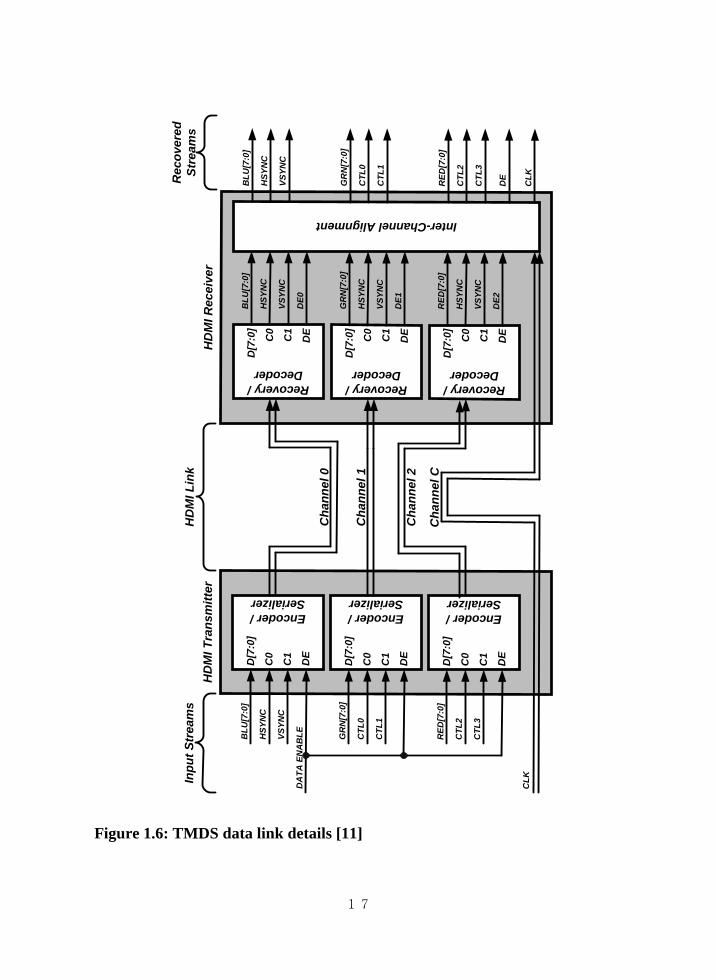
More details of HDMI display link is depicted in Figure 1.6. In the TMDS
transmitter, 8-bit color data and 2-bit control data are serialized in one TMDS data
channel with data enable (DE) signal [11]. In the TMDS receiver, three TMDS
channels are deserialized into original raw data stream with TMDS clock. Various
resolutions and their characteristics for monitors and FPDs are summarized in
Table 1.1 [12]. The TMDS rate per one data channel can be calculated as follows:
TMDS data rate per Ch = (H-pixel + H-blank) (V-pixel + V-blank) (Color depth) (Frame rate) (Overhead)
×× × ×
(1.1)
where overhead means increase of the data rate due to TMDS. The overhead is
same to 8B/10B ANSI coding, 25%. All color depth and frame rate are default
values, 8 bits and 60 Hz, except 1080i resolution. Frame rate for 1080i is 30 Hz.

13
1.2.3 VCSEL-based optical link for HDMI
As data rates of video technology become higher, interconnects for
uncompressed video signals are increasingly harder to make, and more expensive.
Especially, long-haul applications such as HD closed-circuit televisions (CCTV),
large outdoor electronic displays, and interconnects between office display-related
devices or medical equipments, have difficulties in connecting with existing
copper-based cables. Optical interconnects based on low-cost 850-nm vertical-
cavity surface-emitting lasers (VCSELs) and multi-mode fibers (MMFs) are one
of the most promising candidates for uncompressed long-haul video interconnects.
At the most basic level, a VCSEL-based optical link consists of an optical
transmitter, an optical channel, and an optical receiver, as shown in Figure 1.7.
The VCSEL driver converts electrical data to a modulated optical signal, which
propagates through the channel and is converted back into electrical domain at the
optical receiver.
A VCSEL, shown in Figure 1.8, is a semiconductor laser diode which emits
light perpendicular to its top surface. This surface emitting laser offers several
manufacturing advantages over conventional edge-emitting lasers, including
wafer-scale testing ability and dense 2D-array production. The most common and
cost-effective VCSELs are GaAs-based operating at 850nm [13], [14]. 1310-nm

14
GaInNAs-based VCSELs are recently introduced [15], and research-grade devices
near 1550nm are reported [16].
MMF (optical channel) with large core diameters (typically 50 or 62.5μm)
allows several propagating modes, and thus it is relatively easy to couple light into.
This fiber is used in short and medium distance applications such as computing
systems, display interconnects, and campus-scale interconnections. Often
relatively inexpensive VCSELs operating at wavelengths near 850nm are used as
the optical sources for the MMF link. While fiber loss (about 3dB/km for 850-nm
light) can be significant, the major performance limitation of MMF is modal
dispersion caused by the different light modes propagating at different velocities.
Due to modal dispersion, the MMF is used for short and medium distance
applications shorter than 2km.
An optical receiver generally determines the overall optical link performance,
as their sensitivity sets the maximum data rate and amount of tolerable channel
loss, i.e. transmission distance. Typical optical receivers use a photodiode (PD) to
sense the high-speed optical signal and produce currents. This photocurrent is then
converted to a voltage and amplified sufficiently for data resolution. In order to
achieve increasing data rates, sensitive high-bandwidth photodiodes and receiver
circuits are necessary.

15
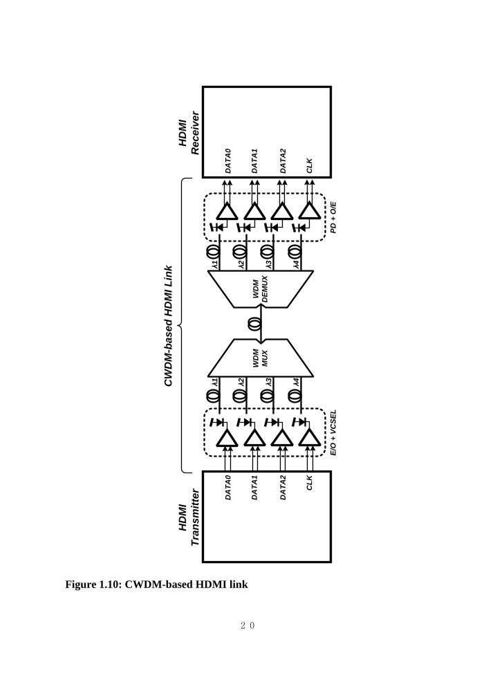
To realize VCSEL-based optical link for HDMI, four VCSELs, MMFs, and
PDs are necessary, as shown in Figure 1.9. As the data rate for HD video requires
at least a few giga-bit per second, not only cable costs become more expensive but
also the skew between channels becomes more serious. To reduce cable costs,
coarse wavelength division multiplexing (CWDM) technique is adopted for
HDMI active optical cable (AOC), as shown in Figure 1.10 [17]. Although the
CWDM system needs only one fiber, extra cost for CWDM MUX and DEMUX is
added and four optical devices are still needed. The optical MUX and DEMUX
are much larger than electrical SERDES ICs, and thus CWDM-based optical link
makes the optical sub-assembly (OSA) module of the AOC be bigger. Besides,
VCSEL reliability can be also issue in productivity angle. VCSEL reliability
potentially poses a serious impediment to very high-speed modulation. Therefore,
use of four optical devices makes the HDMI link be less reliable [18].

16
Figure 1.4: DVI and HDMI cables
HDMITransmitter
HDMIReceiver
TMDS Data 0 (Blue)
TMDS Data 1 (Green)
TMDS Data 2 (Red)
TMDS Clock
Video
Audio
Control Control
Display Control Channel EDIDROM
HDMI Source Component HDMI Sink Component
Video
Audio
Figure 1.5: HDMI display link
17
D[7
:0]
C0
C1
DE
Encoder / Serializer
BLU
[7:0
]
HSY
NC
VSYN
C
D[7
:0]
C0
C1
DE
Encoder / Serializer
GR
N[7
:0]
CTL
0
CTL
1
D[7
:0]
C0
C1
DE
Encoder / Serializer
RED
[7:0
]
CTL
2
CTL
3
DA
TA E
NA
BLE
Inpu
t Str
eam
s
CLK
Cha
nnel
0
Cha
nnel
1
Cha
nnel
2
Cha
nnel
C
D[7
:0]
C0
C1
DE
Recovery / Decoder
BLU
[7:0
]
HSY
NC
VSYN
C
DE0
D[7
:0]
C0
C1
DE
Recovery / Decoder
GR
N[7
:0]
HSY
NC
VSYN
C
DE1
D[7
:0]
C0
C1
DE
Recovery / Decoder
RED
[7:0
]
HSY
NC
VSYN
C
DE2
Inter-Channel Alignment
BLU
[7:0
]
HSY
NC
VSYN
C
GR
N[7
:0]
CTL
0
CTL
1
RED
[7:0
]
CTL
2
CTL
3
DE
CLK
HD
MI L
ink
HD
MI T
rans
mitt
erH
DM
I Rec
eive
r
Rec
over
edSt
ream
s
Figure 1.6: TMDS data link details [11]

18
VCSE
Ldr
v.VC
SEL
Dig
ital
NR
Zda
taR
ecei
ver
PIN
PD
Dig
ital
NR
Zda
ta
MM
F
Opt
ical
tran
smitt
erO
ptic
al c
hann
elO
ptic
al re
ceiv
er
Cur
rent
Driv
ing
Cur
rent
Det
ectio
n
Figure 1.7: VCSEL-based optical link

19
P-Contact
N-ContactN-Contact
LightOut
Topmirror
Bottommirror
Oxidelayer
Gainregion
Figure 1.8: VCSEL cross-section view
VCSEL-based HDMI LinkTMDSTransmitter
DATA0
DATA1
DATA2
CLK
E/O + VCSEL PD + O/E
TMDSReceiver
DATA0
DATA1
DATA2
CLK
Figure 1.9: VCSEL-based HDMI link
20
HD
MI
Rec
eive
r
DA
TA0
DA
TA1
DA
TA2
CLK
HD
MI
Tran
smitt
er DA
TA0
DA
TA1
DA
TA2
CLK
E/O
+ V
CSE
LPD
+ O
/E
λ1 λ2 λ3 λ4
WD
MM
UX
WD
MD
EMU
X
λ1 λ2 λ3 λ4
CW
DM
-bas
ed H
DM
I Lin
k
Figure 1.10: CWDM-based HDMI link

21
1.3 Research goals and organization
The main goal of this research is to investigate and develop single-fiber
HDMI link using electrical SERDES for long-haul display interconnects. With
electrical SERDES, the HDMI link can be realized in single fiber with one pair of
optical device. A serial-link transmitter and receiver with optical analog front-end
(AFE) are designed and realized in standard 0.18-μm CMOS technology. Special
attention is paid to solve the wide-range issue. The single-fiber HDMI link should
support wide-range resolutions from VGA to 1080p, as shown in Table 1.1. One
TMDS data channel exhibits wide data-rate range from 250Mb/s to 1950Mb/s.
Therefore, serial data should cover 750~5850-Mb/s range. This wide-range issue
is solved by the stationary-data-rate architecture.
The dissertation consists of six chapters. In Chapter 2, serial-link architecture
that solves the wide-resolution issue is introduced. Detail system requirements and
solutions are explained. In Chapter 3 and 4, the detailed block-level and
schematic-level circuits for the serial-link transmitter and receiver are respectively
described. Chapter 5 gives implementation and experiment results of the designed
serial-link transmitter and receiver with optical AFEs. Finally, Chapter 6
concludes and summarizes the research carried in this dissertation and gives an
outlook for the future works.

22
Table 1.1 Various resolutions for monitors and FPDs
Resolutions H-pixel (H-blank)
V-pixel (V-blank)
TMDS clock (Pixel clock) [MHz]
TMDS rate/Ch [Mb/s]
Total throughput [Mb/s]
VGA 640 (160)
480 (45) 25.20 252.00 756.00
SVGA 800 (256)
600 (28) 39.79 397.90 1193.70
XGA 1024 (320)
768 (38) 65.00 649.96 1949.88
SXGA 1280 (408)
1024 (42) 107.96 1079.64 3238.93
WXGA 1280 (400)
800 (31) 83.76 837.65 2512.94
UXGA 1600 (560) 1200 (50) 162.00 1620.00 4860.00
1080i 1920 (280)
1080 (45) 74.25 742.50 2227.5
1080p (full HD)
1920 (280)
1080 (45) 148.50 1485.00 4455.00
WUXGA 1920 (672)
1200 (45) 193.52 1935.22 5808.67
1) H-pixel: the number of horizontal pixels, H-blank: the number of horizontal blank pixels
2) V-pixel: the number of vertical pixels, V-blank: the number of vertical blank pixels
3) Color depth for all resolutions is 8 bits.
4) Frame rate (refresh rate) for all resolutions is 60 Hz except 1080i. Frame rate for 1080i is 30 Hz.

23
CHAPTER 2
SERIAL-LINK ARCHITECTURE
2.1 Single-fiber HDMI link requirements
Figure 2.1 shows the original HDMI link architecture and the single-fiber
VCSEL-based HDMI optical link using electrical SERDES, which is the main
goal of this dissertation. In the original HDMI link, raw input streams are
converted into three TMDS data through HDMI transmitter. And these TMDS
data are recovered to the raw data. The raw data include RGB signals (RED[7:0],
BLU[7:0], GRN[7:0]), vertical synchronization signal (VSYNC), horizontal
synchronization signal (HSYNC), and data enable signal (DE). The HDMI
transmitter consists of three 10:1 serializer and TMDS encoder, and the HDMI
receiver is composed of 1:10 de-serializer, TMDS decoder, and inter-channel
alignment block. The proposed SERDES-based HDMI link is very cost-effective
system compared with basic 4-channel HDMI optical link and CWDM-based
HDMI link. With existing commercial products, system costs of three HDMI
optical links are summarized in Table 2.1.
The single-fiber VCSEL-based HDMI optical link using electrical SERDES
deals with three TMDS data (TMDS DATA0, DATA1, and DATA2) and one
24
TMDS clock as the final inputs and outputs. The serial-link transmitter converts
three parallel data into serial data with TMDS clock. The serial-link transmitter
also includes VCSEL driver (E/O) which drives an off-chip VCSEL for optical
interconnects. This serialized optical signal is transmitted through the optical
channel (MMF), and arrived at the PIN PD. The incident optical signal is changed
into electrical current by the PIN PD. This current signal is converted into voltage
signal by optical receiver (O/E). The serialized signal is again parallelized into
TMDS data and clock by the serial-link receiver.
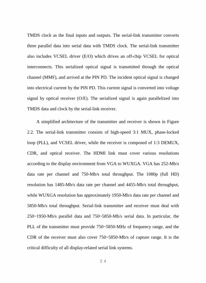
A simplified architecture of the transmitter and receiver is shown in Figure
2.2. The serial-link transmitter consists of high-speed 3:1 MUX, phase-locked
loop (PLL), and VCSEL driver, while the receiver is composed of 1:3 DEMUX,
CDR, and optical receiver. The HDMI link must cover various resolutions
according to the display environment from VGA to WUXGA. VGA has 252-Mb/s
data rate per channel and 750-Mb/s total throughput. The 1080p (full HD)
resolution has 1485-Mb/s data rate per channel and 4455-Mb/s total throughput,
while WUXGA resolution has approximately 1950-Mb/s data rate per channel and
5850-Mb/s total throughput. Serial-link transmitter and receiver must deal with
250~1950-Mb/s parallel data and 750~5850-Mb/s serial data. In particular, the
PLL of the transmitter must provide 750~5850-MHz of frequency range, and the
CDR of the receiver must also cover 750~5850-Mb/s of capture range. It is the
critical difficulty of all display-related serial link systems.

25
In the PLL side, there are many candidates to meet the wide-range
requirements. A multi-band PLL using multi voltage-controlled oscillators
(VCOs) can be a solution. One of the possible solutions is using octave VCO with
programmable frequency divider [19]. Wideband VCO having 2925~5850-MHz
tuning range with programmable frequency divider can make continuous
750~5850-MHz clocks, however, it is not easy to realize.
In the CDR side, wide-range CDR is necessary. The wide-range CDR has to
detect the bit rate of the incoming data without harmonic lock. A wide-range
frequency detector is an essential block to recover the data with a wide-range data
rates. In frequency detection process, complex-rate detection with finite-state
machine (FSM) is needed to prevent from harmonic lock [20]. Performance,
accuracy, and stability also depend on the data-pattern characteristics, such as run
length, DC balance, and coding schemes [21-22]. HDMI serial link using wide-
band PLL and CDR has the merit of being more energy-efficient system using
adaptive supply regulation according to the data rates [23]. However, it is difficult
to realize and it is sensitive to data patterns, and needs more expensive CMOS
process to realize the high-performance frequency detector. To provide full video
resolutions without wide-range PLL and CDR, we proposed stationary-data-rate
(SDR) architecture having a fixed serial data rate for wide-range input. Input and
output requirements for stationary-data-rate scheme are summarized in Table 2.2.

26
Table 2.1 System cost of HDMI optical interconnects
Basic HDMI Optical
Link CWDM-based HDMI
Link SERDES-based
HDMI Link
Number of Fiber Channel 4 1 1
Components (number of
components)
Laser, PD (4) Optical AFE (4) Fiber (4)
Laser, PD (4) Optical AFE (4) Fiber (1) CWDM (1)
Laser, PD (1) Optical AFE (1) Fiber (1) SERDES (1)
Link Cost for 1km MMF
Laser, PD = $320 AFE= $144 Fiber = $600 Total = $1,064
Laser, PD= $320 AFE= $144 Fiber = $150 CWDM = $660 Total = $1,274
Laser, PD = $80 Fiber = $150 SERDES w/ AFE = $100 Total = $330
Link Cost for 10km SMF
Laser, PD = $320 AFE = $144 Fiber = $8,000 Total = $8,464
Laser, PD = $320 AFE = $144 Fiber = $2,000 CWDM = $660 Total = $3,124
Laser, PD = $80 Fiber = $2,000 SERDES w/ AFE = $100 Total = $2,180
Pros. - Easy to implement
- Good for long-haul SMF link
- BW limit of IC = 1/4 of throughput
- Good for high-performance & high-speed link
- High reliability
- Low cost - High reliability - High system integration level - Good for short-haul or low-cost MMF link
Cons. - High cost - Low reliability
- High cost for short link - Low system integration level (CWDM MUX and DEMUX has large size)
- BW limit of electrical circuit (Max. speed = 40Gb/s)

27
Table 2.2 Requirements of single-fiber HDMI link
Divisions Contents Remark
Input stream data
rate
(TMDS data)
250Mb/s ~
1950Mb/s
VGA to WUXGA
including 1080p
Input clock
frequency
(TMDS clock)
25MHz ~
195MHz
1/10 frequency
compared to the
TMDS data rate
Serial data rate
w/o overhead
5850Mb/s
(1950Mb/s x
3Ch)
determined w.r.t.
highest video
resolution (WUXGA)
Serial data rate
w/ overhead
6240Mb/s
(5850Mb/s x
64/60)
Including 64/60
overhead
Input/Output
electrical
specification
Current-mode
logic
3.3V pull-up with AC
coupling (due to
TMDS electrical
specification)
Serial-link
electrical
specification
(miss, MMF)
Current-mode
logic
1.8V pull-up with AC
coupling (due to
internal core power
supply)

28
DATA0
DATA1
DATA2
TCLK
DATA0
DATA1
DATA2
TCLK
HD
MI S
eria
lizer
DATA0
DATA1
DATA2
TCLKHD
MI D
eser
ializ
er
MMF
D[7:0]
C0
C1
DE Enco
der /
Se
rializ
erBLU[7:0]
HSYNC
VSYNC
D[7:0]
C0
C1
DE Enco
der /
Se
rializ
er
GRN[7:0]
CTL0
CTL1
D[7:0]
C0
C1
DE Enco
der /
Se
rializ
er
RED[7:0]
CTL2
CTL3
DATA ENABLE
Input Streams
CLK
TMDS DATA0
TMDS DATA1
TMDS DATA2
TMDS CLK
D[7:0]
C0
C1
DERec
over
y /
Dec
oder
BLU[7:0]
HSYNC
VSYNC
DE0
D[7:0]
C0
C1
DERec
over
y /
Dec
oder
GRN[7:0]
CTL0
CTL1
DE1
D[7:0]
C0
C1
DERec
over
y /
Dec
oder
RED[7:0]
CTL2
CTL3
DE2
Inte
r-C
hann
el A
lignm
ent
BLU[7:0]
HSYNC
VSYNC
GRN[7:0]
CTL0
CTL1
RED[7:0]
CTL2
CTL3
DE
CLK
HDMI LinkHDMI Transmitter HDMI Receiver
RecoveredStreams
DATA0
DATA1
DATA2
TCLK
E/O O/E
Serial-Link Transmitter
Serial-Link Receiver
VCSEL PIN PD
Figure 2.1: Single-fiber VCSEL-based HDMI link using serial-link
transmitter and receiver compared with original HDMI link

29
Serial-link Receiver
TMDS DATA0
TMDS DATA1
TMDS DATA2
TMDS CLK
TMDS DATA0
TMDS DATA1
TMDS DATA2
TMDS CLK
3:1MUX
1:3DEMUX
E/O O/E
MMF
Serial-link Transmitter
VCSEL PIN PD
CDRPLL
Figure 2.2: Simplified architecture of the transmitter and receiver

30
2.2 Proposed serial-link architecture: stationary-data-rate scheme
In this dissertation, SDR architecture is proposed to realize VCSEL-based
HDMI serial link without wide-range PLL and CDR. In short, all parallel data
having wide-range data rates are serialized into a fixed data rate. The stationary
serial data rate is determined for the highest resolution, WUXGA
(1950Mb/s/channel).
Before we start the discussion, explanation about illuminating prefixes and
suffixes, T-, S-, -10, -64, and so on, is required. For SDR scheme, there are two
clock domains. One is synchronized with TMDS data and clock, namely TMDS
clock domain (T-domain), and the other is based on stationary serial data, namely
stationary clock domain (S-domain). T-domain clock (TCLK) varies according to
the incoming TMDS data rate, while S-domain clock (SCLK) is always fixed at
6.24GHz. A suffix number means dividing factor, for example, SCLK64 means
stationary clock divided by 64 and TCLK10 means TMDS clock divided by 10.
We summarize various clock names and their description in Table 2.2.
Figure 2.3 shows the serial-link transmitter architecture to realize the SDR
scheme. Serial-link transmitter consists of three CDRs with 1:20 DEMUX, digital
processing block, 64:1 MUX with LC-type PLL, and optical transmitter AFE for
VCSEL. Digital signal processing is needed for implementing SDR scheme. For

31
digital processing, high-speed TDMS data should be parallelized. Each TMDS
data is parallelized to 20-bit wide data by 1:20 DEMUX. These 60-bit parallel
data go to a digital processing block having under 100-Mb/s data rate. TMDS
clock has one tenth frequency of TMDS data rate, thus it cannot be directly used
as a clock of 1:20 DEMUX. Besides TMDS clock has no optimized phase
relationship with TMDS data. Thus CDR circuit is necessary to guarantee the
frequency and the phase relationship for de-multiplexing. The CDR has to have
wide capture range to cover all the video resolutions from 250Mb/s to 1950Mb/s.
The ring-type PLL-based architecture with programmable frequency divider is
used for this CDR. Programmable dividing factor is determined by a range
detector of digital processing block.
In the digital processing block, many complicated functions must be
conducted for SDR scheme. First it is the range detection. The range detector
compares T-domain with S-domain, and generates 2-bit range codes having
frequency range information. These range codes determine the dividing factor of
input CDRs into 1, 2, or 4. Second is data alignment. Incoming 60-bit data and
three clocks come from CDRs. Each 20-bit data and output clock of the CDR are
synchronized each other, however, three parts of data group have no phase relation.
Data alignment block looks for rising edges of the CDR output clocks
(TCLK20_0, TCLK20_1, and TCLK20_2) near the TCLK10. When all the rising
edges are detected, the data alignment block generates divider reset signal for

32
frequency divider of the input CDRs. And then all three frequency dividers of the
input CDRs are reset to guarantee the phase relationship.
Third is frequency domain conversion. This function is the most important in
this SDR scheme. As mentioned above, there are two clock domains. One is T-
domain based on TMDS clock, and the other is S-domain synchronized to
stationary clock referenced on external crystal oscillator (X-TAL). Stationary
clock having 6.24GHz is produced by LC-PLL with X-TAL reference clock and
frequency dividing factor of 256. Frequency domain conversion means data
streams synchronized with T-domain are converted into data streams synchronized
with S-domain. In other words, 60-bit wide data having 12.5~97.5-Mb/s rate is
changed to 97.5-Mb/s fixed data. Therefore 97.5-Mb/s fixed data exhibits empty
timing slots. By filling out dummy data to empty timing slots, these underflows
can be solved. We use frame-based signal processing for effective and simple
dummy filling. Parallel 60-bit wide data stream and 4-bit header compose one
frame. Two types of 4-bit header indicate whether this frame is real data or
dummy data. To determine how many dummy data are needed, we create data
valid (DAV) ratio. DAV ratio is defined to the ratio of the real timing slots
compared with total time, that is, it can be expressed as follows:
6420 20 ) (
SCLKTCLK
e) Frame Rat(Staionary Rate) / (TMDS DataRatioDAV == (2.1)

33
DAV signal indicates the incoming data goes through how much underflow is.
High DAV signal means that this frame is real.
For example, TMDS data rate is 1462.5Mb/s. Then parallelized data rate is
73.125Mb/s and stationary frame rate is 97.5MHz, and DAV ratio is 3/4. Frame
timing diagram in this case is depicted in Figure 2.4. First-in first-out (FIFO) is
used for clock-rate conversion. TCLK20 is used as read clock of FIFO, while
SCLK64 is used as write clock of FIFO. The output of FIFO (real data) and
dummy data go through the selecting MUX. The DAV signal is used as the
control signal in the selecting MUX. Dummy data are generated by the dummy
encoder, which includes frequency range information. The frequency range of
input CDR from 200MHz to 2000MHz (including margin) is separated into three
parts, 2000~1000MHz, 1000~500MHz, and under 500MHz. 2-bit range codes
represent each frequency range. According to these range codes dummy data
patterns have difficult. 60-bit dummy data for one dummy frame consists of
twelve times recursive 5-bit patterns. In summary, FIFO, DAV encoder, selecting
MUX, header encoder, and dummy encoder compose the frequency domain
conversion block.
The fourth function of digital processing block is scrambling. To guarantee
the transition density for clock extraction of the serial-link receiver, 60-bit wide
data are encoded to 215-1 PRBS (PRBS15) data by 4-parallel 15-wide scramblers.

34
After digital processing, frame-based 64-bit wide parallel signals having
stationary 97.5-Mb/s data rate are serialized by 64:1 MUX and LC-type PLL. 64:1
multiplexing is done in two steps, first 64:4 with CMOS logic and second 4:1 with
CML. To minimize power consumption, CML is used only when necessary for
high-speed MUX, while low-speed MUX uses CMOS logic. Low-speed 64:8
MUX is based on the shift-register architecture for chip area reduction, while
high-speed 8:4 MUX and 4:1 MUX are designed with the tree architecture for
power reduction [24]. LC-type PLL generates 6.24-GHz full-rate clock with
20.375-MHz X-TAL for low-jitter characteristics. Quality of this full-rate clock
determines link performances, such as bit error rate (BER), transmission distance,
and optical sensitivity. The electrical serial signal is converted into optical signal
by optical transmitter and off-chip 850-nm VCSEL, and this optical NRZ signal is
transmitted to the serial-link receiver. Summary chart explaining signal path and
control signal of the serial-link transmitter is shown in Figure 2.5.
The serial-link receiver architecture for SDR scheme is described in Figure
2.6. It consists of optical receiver AFE, 1:64 DEMUX with PLL-based CDR,
digital processing block, and three 20:1 MUXs with fractional PLL for TMDS
clock recovery. Optical receiver converts the incident light into electrical NRZ
data having fixed output swing (400mVpp). The LC-PLL-based CDR extracts
full-rate clock and recovers data with 1:64 DEMUX. The CDR has dual-loop
architecture. One is the frequency adjustment loop based on X-TAL and phase

35
frequency detector (PFD), and the other is the phase alignment loop with a bang-
bang phase detector (BBPD).
In the receiver digital processing block, inverse of the transmitter functions
are done. The first step is sequence alignment. It is finding out where the first bit
of the frame is. A barrel shifter is used for sequence alignment. The barrel shifter
searches for recursive header bit per 64 bits. The second step is descrambling the
transmitted data. 60-bit data except 4-bit header are descrambled. These 60-bit
wide data are now synchronized with S-domain. The third step is inversely
frequency domain conversion from S-domain to T-domain in the same way as the
transmitter. However there is no T-domain clock in the receiver. T-domain clock
of the transmitter is the physical input, while T-domain clock of the receiver
should be autonomously generated. Information on TMDS data rate in the receiver
is only on the 4-bit of header. As mentioned earlier, 4-bit header has two kinds of
code, ‘1100’ or ‘0011’. ’1100’ means this frame is real, or vice versa. After
sequence alignment, we can separate one frame into 4-bit header and 60-bit data
stream. Thus we can recover DAV signal. Now we know the DAV ratio, then we
get the TMDS data rate by comparing S-domain clock. If DAV ratio is 1/4,
TCLK20 is one fourth of SCLK64, i.e. 24.375MHz. SCLK64 is not always
multiples of TCLK20, therefore output PLL for generating TMDS clock should be

36
fractional. In a similar way, 2-bit range codes are discovered from specific dummy
data patterns.
Fractional PLL (Δ-Σ PLL, delta-sigma PLL) is exploited for recovering the
TMDS clock. From information on DAV ratio we can determine a dividing factor
of PLL having the fractional value. The reference clock of this PLL is based on
stationary clock (SCLK64). In summary, TMDS clock is generated from a clock
synchronized to SCLK64 with fractional dividing factor which is determined by
DAV signal. With recovered TMDS clock, sequence-aligned 60-bit wide real data
are serialized in three TMDS data by three 20:1 MUXs. A signal flow chart is
shown in Figure 2.7. In this chapter, we discussed the stationary-data-rate
architecture in a block level. Detailed descriptions of each building block will be
explained in the next two chapters.

37
Table 2.3 Clock description
Clock name Description Frequency
or data rate
TCLK The output clock of transmitter input CDR synchronized with TMDS clock. It varies as video resolutions.
250 ~ 1950MHz
TCLK10
TMDS clock behind TMDS clock buffer The frequency is same to input TMDS clock having one tenth of TMDS data rate.
25 ~ 195MHz
TCLK20 TCLK divided by 20 12.5 ~ 97.5MHz
TCLK20 0~3
TCLK divided by 20 (output of transmitter input CDRs, synchronized to the 20-bit parallel data from CDRs)
12.5 ~ 97.5MHz
SCLK
Stationary clock based on external crystal oscillator (X-TAL). It is determined by maximum input video resolution (now WUXGA).
6240MHz
SCLK64 SCLK divided by 64 97.5MHz
SCLK256 SCLK divided by 256 (same to frequency of X-TAL) 24.375MHz

38
TMD
S D
ATA
0
1:20
D
EMU
Xw
/ CD
R
TMD
S D
ATA
1
1:20
D
EMU
Xw
/ CD
R
TMD
S D
ATA
2
1:20
D
EMU
Xw
/ CD
R
TMD
SC
lock
Buf
fer
TMD
S C
LK
20 20 20
TCLK
20_0
TCLK
20_1
TCLK
20_2
TCLK
10
Dig
ital P
roce
ssin
g
1. R
ange
det
ectio
n2.
Dat
a al
ignm
ent
3. F
req.
dom
ain
conv
ersi
on
- FIF
O
- Hea
der e
ncod
ing
(
64/6
0 ov
erhe
ad)
- D
umm
y en
codi
ng4.
Scr
ambl
ing
6464
:1M
UX
1
LC-P
LL(6
.24G
Hz)
X-TA
LSC
LK64
E/O
VCSE
L
Seria
l-Lin
k Tr
ansm
itter
Figure 2.3: Serial-link transmitter architecture for SDR scheme

39
...
00 11 Dummy Frame
Real Data Frame
11 00 Real Data Frame
Real Data Frame
DA
V si
gnal
4-bi
t hea
der
60-b
it da
ta
stre
am
Fram
e ra
te =
97.
5Mb/
s
00 11 Dummy Frame
Dummy Frame
Dummy Frame
11 0011 00
11 0011 00
11 0011 00
11 0011 00
11 0011 00
11 0000 11
00 1111 00
11 00
Real Data Frame
Real Data Frame
Real Data Frame
Real Data Frame
Real Data Frame
Real Data Frame
Real Data Frame
Real Data Frame
Real Data Frame
Real Data Frame
Real Data Frame
Figure 2.4: Frame timing diagram with DAV signal
40
250~1950Mb/s TMDS data (3ea)25~195MHz TMDS clock (1ea)
1:20 DEMUXw/ CDR (3x)
TMDS data0, data1, data2
Data alignment
60-bit not-aligned dataTCLK20
divider reset
Range detection
TCLK20 SCLK64
TCLK10
range<1:0>
Dummy encoding
60-bit aligned data
FIFO
TCLK20(write clk)
SCLK64(read clk)
DAV gen.0 1DAVsignal
64:1 MUX Headerencoder
4-bit header
60-bit data
LC-PLL(6.24GHz)
X-TAL(24.375MHz)
E/O(VCSEL drv.)
6.24Gb/soptical signal
real framedummy frame
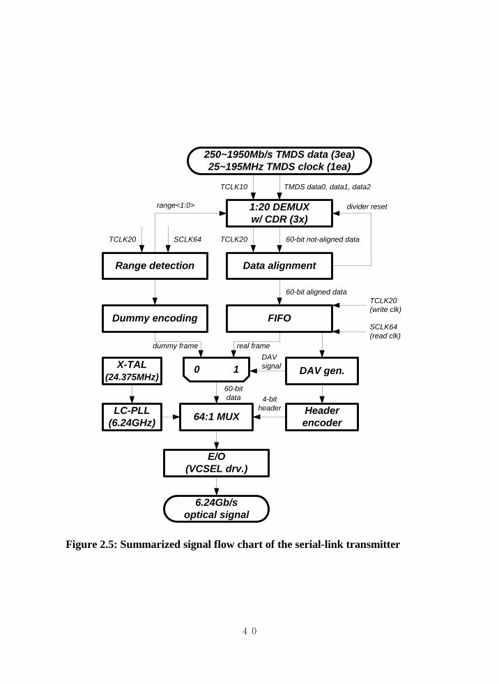
Figure 2.5: Summarized signal flow chart of the serial-link transmitter

41
O/E
PIN
PD1:
64D
EMU
X
LC-P
LL
base
d C
DR
(6.2
4GH
z)
1
X-TA
L
Dig
ital P
roce
ssin
g
1. S
eque
nce
Alig
nmen
t
(Bar
rel s
hifte
r)2.
Des
cram
blin
g3.
Fre
q. d
omai
n co
nver
sion
- F
IFO
- D
AV
reco
verin
g fr
om
h
eade
r4.
Ran
ge d
etec
tion
(D
umm
y de
codi
ng)
64
SCLK
64
20:1
MU
X
20:1
MU
X
20:1
MU
X
∆-Σ
PLL
TCLK
1020 20 20
TMD
S D
ATA
0
TMD
S D
ATA
1
TMD
S D
ATA
2
TMD
S C
LK
Seria
l-Lin
k R
ecei
ver
Figure 2.6: Serial-link receiver architecture for SDR scheme
42
6.24Gb/soptical signal
O/E(Optical receiver)
1:64 DEMUX 6.24Gb/s CDR
Sequence align(Barrel shifter) DAV recovering
FIFOTCLK20
(read clk)
SCLK64(write clk)
X-TAL(24.375MHz)
60-bit aligned data
4-bitheader
Range detection
DAV signal
∆-Σ PLL
range<1:0>60-bit FIFO output
60:3MUX
250~1950Mb/s TMDS data (3ea)25~195MHz TMDS clock (1ea)
Three TMDS data TMDS Clock
Figure 2.7: Summarized signal flow chart of the serial-link receiver

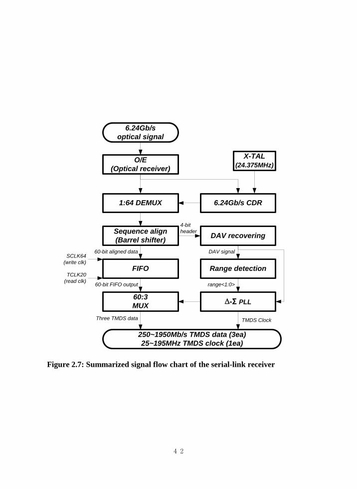
43
CHAPTER 3
SERIAL-LINK TRANSMITTER
3.1 Transmitter structure
Figure 3.1 shows block diagrams of the serial-link transmitter. According to
the synchronized clocks and roles, it can be divided into three parts: transmitter
input stage, transmitter digital stage, and transmitter output stage. First the
transmitter input stage is synchronized with T-domain, and its vital role is slowing
down three TMDS input data for the digital stage. The digital stage has digital
processing blocks including data aligner, range detector, dummy encoder, FIFO,
selecting MUX, header encoder, and scrambler. The digital stage connects T-
domain and S-domain. The transmitter output stage generates 6.24-Gb/s serial
data and 6.24-GHz stationary clock based on external X-TAL. It includes 6.24-
GHz LC-type PLL, 64:1 MUX, and optical transmitter AFE (VCSEL driver) for
optical interconnect.

44
250~
1950
Mb/
sTM
DS
Dat
a (x
3)
25~1
95M
Hz
TMD
S C
lock
60
Dat
aA
ligne
r
FIFO
60
Dum
my
Enco
der
5x12
Hea
der
Enco
der
1 0
60
Scra
mbl
er60
64
4
Dig
ital
Proc
essi
ng B
lock
6.24
-GH
zLC
-PLL
X-TA
L(2
3.37
5MH
z)
VCSE
LD
rv.
VCSE
L
64:1
MU
X6.
24 G
b/s
Seria
lized
Dat
a
%64
SCLK
64
DA
V Si
gnal
CD
R(x
3)w
ith1:
20D
EMU
X
Dat
aO
ut
TCLK
20 Out
On
Chi
pO
ff-C
hip
Sele
ctin
gM
UXs
(x60
)
Hea
der
Ran
geD
et.
Buf
fere
dC
lkTC
LK20
Ran
ge<1
:0>
SCLK
TCLK
10
Div
ider
Res
et3
Dum
my
read
writ
e
Tran
smitt
er in
put s
tage
Tran
smitt
er d
igita
l sta
geTr
ansm
itter
out
put
stag
e
Figure 3.1: Three parts of the serial-link transmitter

45
3.2 Transmitter input stage
The transmitter input stage includes TMDS input buffer, TMDS clock buffer,
three ring-PLL-based CDRs, and three 1:20 DEMUXs. And the input stage is
synchronized with T-domain. A vital role of the input stage is generating parallel
60-bit data from three TMDS input data for next digital processing. Figure 3.2
shows the block diagram of TMDS input stage. Through buffering, three TMDS
inputs and one TMDS clock go into 1:20 DEMUX and ring-PLL-based CDR.
Ring-PLL-based CDR generates full-rate clock (TCLK) referenced on TMDS
input clock having one tenth frequency of data. Also this TCLK and TMDS input
data have optimal phase relations produced by CDR.
3.2.1 TMDS input buffer and clock buffer
TMDS coding scheme is electrically same as CML, and it is DC coupled and
terminated to 3.3-V supply. For this, all TMDS-based inputs and outputs use 3.3-
V I/O. Because core circuits must operate under 1.8-V supply, these 3.3V-
terminated signals should be leveled down. Figure 3.3 shows TMDS input buffer
for data. A conventional common-drain buffer is used for level-shifting. To deal
with 3.3V signal in a 0.18-μm CMOS technology, thick-gate transistors (TPM1,
TPM2, TNM1, and TNM2) are used. By using the resistor ratios rather than
absolute values, effects on process variations are minimized. Finally, level-shifted
differential signals are converted into 1.8-V pull-up signals by CML buffer. Figure

46
3.4 depicts TMDS clock buffer. Unlike TMDS data, TMDS clock should be
converted into single-ended signal because the next PFD requires full-swing
CMOS signal. TMDS clock buffer consists of TMDS input buffer and CML-to-
CMOS buffer with scaling inverters.
3.2.2 Wide-range ring-PLL-based dual-loop CDR with 1:20 DEMUX
A full-rate clock or half-rate 4-phase clocks are required for de-multiplexing
TMDS data into 20-bit slow data. Besides, parallelization always requires well-
defined phase relations between data and sampling clock. Therefore PLL-based
clock-and-data-recovery circuit is required. As you can see in Table 1.1, TMDS
data has a rate between 250Mb/s and 1950Mb/s according to the incoming video
resolutions. Thus CDR should cover these wide ranges. To provide wide capture
range, we select the ring-type VCO with programmable frequency divider.
Considering a design margin, ring VCO should be able to oscillate at 250MHz to
2000MHz. To relax the VCO design, a programmable frequency divider is used.
The entire data-rate range is separated into three ranges: 250~500MHz,
500~1000MHz, and 1000~2000MHz. Each range is represented by the range code
from the range detector. The range detection for the incoming data is easy to
realize because we have another definite reference clock from an external crystal
oscillator. If ring VCO can cover the frequency range from 1000MHz to

47
2000MHz, the PLL can generate any frequency below 2000MHz with a
programmable dividing factor. The programmable dividing factor is 1, 2, or 4 with
respect to three separating frequency ranges. For the incoming data of 250Mb/s,
800Mb/s, and 1620MHz, for example, the ring VCO is locked to 1GHz with
dividing factor of 4, 1.6GHz with 2, and 1.62GHz with 1.
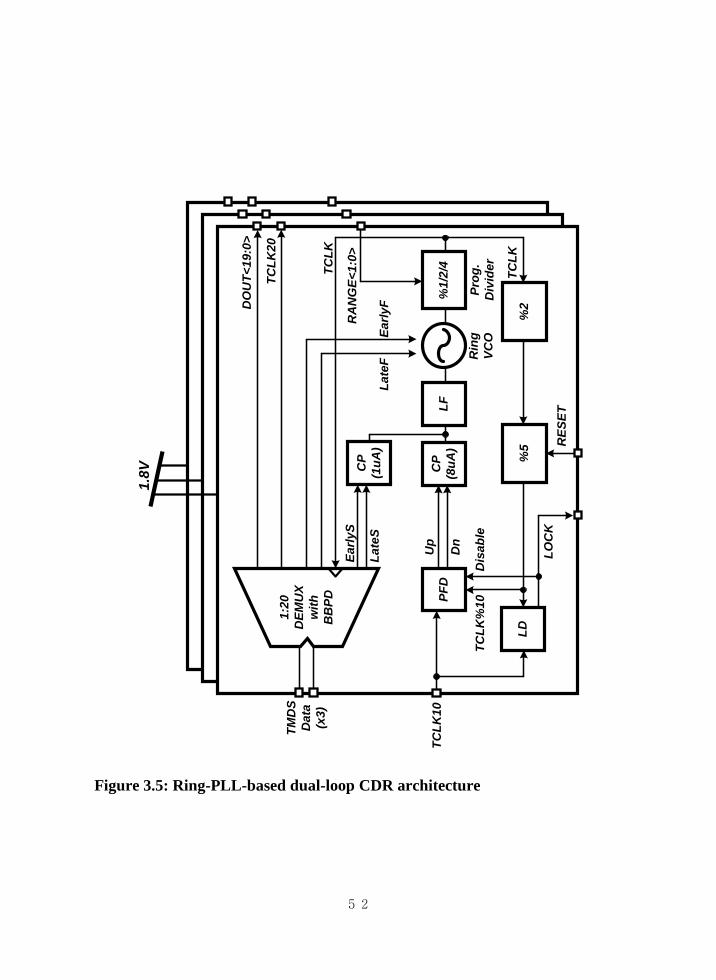
Figure 3.5 shows the ring-PLL-based CDR. The CDR consists of dual-loop
architecture. One loop performs frequency acquisition, and the other phase
alignment. The frequency acquisition loop is composed of PFD, charge pump(CP),
loop filter(LF), ring-type VCO, programmable frequency divider, lock
detector(LD) and frequency divider having fixed dividing factor of 10. If VCO
output frequency equals tenth of TCLK10, LD generates lock signal (LOCK). And
PFD is disabled. In the phase alignment loop, BBPD drives CP instead of PFD.
Charge-pump current is comparatively high (8μA) for fast frequency acquisition,
while charge-pump current for phase alignment is 1μA. VCO output frequency is
controlled by two paths: integral path and proportional path. The integral path
controls frequency through integration of charge-pump current, while proportional
path directly controls the ring-VCO currents. The BBPD generates fast bang-bang
signals (EarlyF and LateF) for proportional path and slow bang-bang signals
(EarlyS and LateS) for integral path. By separating the control path of BBPD, the
feedback-loop latency can be reduced and the bandwidth requirement of the CP
can be relaxed [25]. 1:20 DEMUX with BBPD is depicted in Figure 3.6. It is

48
separated into three parts: 1:2 tree-type DEMUX with fast and slow BBPD, 2:4
tree-type DEMUX, and 4:20 shifter-resistor-type DEMUX.
Detail 1:2 DEMUX with BBPD is shown in Figure 3.7. It consists of 1:2
DEMUX with slow BBPD for integral control, fast BBPD for proportional control,
and decimation gate. CMOS logic is used for power reduction. Sense amplifier is
exploited for conversion CML to CMOS logic, as shown in Figure 3.8. To
generate bang-bang signals, three samples (A, T, and B) are required. Fast BBPD
compares TMDS data with TCLK, while slow BBPD compares de-multiplexed
data with divided TCLK2. Basic operations and truth table of the BBPD logic is
depicted in Figure 3.9. As the figure depicts, (A) means first rising-edge sampled
data, (B) means next rising-edge sampled data, and (T) means falling-edge sample
data, i.e. transition. In the inset table of Figure 3.9, state 0 and 7 mean relation
between data and clock is optimum or there is no transition. State 2 and 5 are
generally impossible states. State 1 and 6 indicate clock leads data, thus late signal
is generated to slow clock down, and vice versa. Decimation gate is used to relax
speed limit of charge pump. 2, 4, or 8 counters according to the range codes count
how many TCLK2 exits during slow bang-bang signal (Early2 or Late2) is high,
and each carry of the counters makes the other-side D flip-flops be disable to
prevent from simultaneous bang-bang signals. These decimated slow bang-bang
signals (EarlyS and LateS) go into small CP having 1-μA pumping current.

49
Three-stage inverter-type ring-VCO is depicted in Figure 3.10. The VCO is
controlled by integral tuning voltage (VtuneI) and fast bang-bang signals (EarlyF
and LateF). VtuneI affects on a gate voltage of PM16 through current mirroring
(PM1, PM2, NM1, NM2, NM3, NM4, NM5, and PM15). EarlyF can also control
the gate voltage of PM16, while LateF control the source voltage of PM16.
EarlyF and LateF drive switching transistors (PM7, PM8, PM9, and PM10) with
current sources driven by VtuneI. By controlling the currents flowing through
PM16, transconductance of the inverters, i.e. delay time of the inverters, can be
adjusted to the target frequency. The final output clock (TCLK) exhibits full swing
through inverter arrays, while the output of three-stage VCO has lower swing (1-V
swing) to relax speed limits.

50
3.3V 1.8V
TMDSCLK
Buffer
1:20DEMUX
(x3)
DOUT<19:0>
TCLK20TMDS Data (x3)
RANGE<1:0>
TCLK10
3.3V 1.8V
TMDSBuffer
(x3)
TMDS Clock
TCLK
1.8V
1.8V
Ring-PLL-based CDR(x3)
3
3
Figure 3.2: TMDS input stage
50Ω
I/O Supply = 3.3V
PowerDown
TMDSInput CML
Output
TPM1 TPM2
TNM1 TNM2
RS1
RS2
RD
Itail
Core Supply = 1.8V
50-Ω termination Level shifting CML buffer
NM1 NM2
Figure 3.3: TMDS input buffer for 3.3-V I/O

51
50Ω
I/O S
uppl
y =
3.3V
Pow
erD
own
TMD
SIn
put
TPM
1TP
M2
TNM
1TN
M2
RS1 RS2
RD
Itail
Cor
e Su
pply
= 1
.8V
50-Ω
term
inat
ion
Leve
l shi
fting
CM
L bu
ffer
NM
1N
M2
Itail
Cor
e Su
pply
= 1
.8V
NM
1N
M2
PM1
PM2
1x2x
8x
CM
L-to
-CM
OS
with
CM
OS
inve
rter
s
TCLK
10
Figure 3.4: TMDS clock buffer with CML-to-CMOS conversion
52
PFD
CP
(8uA
)LF
%2
%1/
2/4
Early
S
Late
S
1:20
DEM
UX
with
BB
PD
DO
UT<
19:0
>
TCLK
20
Early
FLa
teF R
ing
VCO
LD
TMD
S D
ata
(x3)
LOC
K
RA
NG
E<1:
0>
TCLK
10U
p
Dn
%5 R
ESET
TCLK
TCLK
Prog
. D
ivid
er
1.8V C
P(1
uA)
TCLK
%10
Dis
able
Figure 3.5: Ring-PLL-based dual-loop CDR architecture

53
1:2
DEM
UX
w/
BB
PD
2:4
DEM
UX
4TM
DS
Dat
aTC
LK2
Dat
a<1:
0>
Dec
imat
ion
(x2/
x4/x
8)
TCLK
44:
20
DEM
UX
Early
FLa
teF
Early
SLa
teS
20
TCLK
20
Ran
ge<1
:0>
TCLK
Figure 3.6: 1:20 DEMUX with BBPD

54
TCLK
Sens
eA
mpl
ifier
with
FF1
x
TMD
SD
ata
XNO
R2
2xD
FFC
MO
S 1x
XNO
R2
2xD
FFC
MO
S 1x
Late
F
Early
F
Sens
eA
mpl
ifier
with
FF1
x
DFF
CM
OS
1x
1x4x
2x
2x
6x 6x
LATC
HC
MO
S 1x
6x1:
2D
EMU
X
1:2
DEM
UX
A T B1x 1x
Dou
t<1>
Dou
t<0>
BB
PD
A T BB
BPD
DFF
CM
OS
1x
%2
2x4x
16x
TCLK
_ATB
2x4x
TCLK
2
NA
ND
22x
1x 1x 1x 1xN
AN
D2
2x
NA
ND
22x
NA
ND
22x
LOC
K
DFF
CM
OS
1x DFF
CM
OS
1x
1xEa
rly2
1xLa
te2
DFF
CM
OS
1x
2/4/
8C
ount
er
Early
2TC
LK_A
TBRan
ge<1
:0>
DFF
CM
OS
1x
2/4/
8C
ount
er
Late
2TC
LK_A
TBRan
ge<1
:0>
Dis
able
Dis
able
Early
S
Late
S
Dec
imat
ion
Gat
e
1:2
DEM
UX
with
Slo
w B
ang-
Ban
g PD
Fast
Ban
g-B
ang
PD
TA
B
T21
T22
Figure 3.7: 1:2 DEMUX with BBPD and decimation gate

55
CLK
INP
OUTMx2x4 x2 x4
INM
OUTP
PM1 PM3PM2 PM4
NM1 NM2
PM5
PM6
PM7
NM3
Figure 3.8: Clocked sense amplifier
A BT
1) Optimum sampling
0 or 1 1 or 0
Early = B T
A T B Early Late Remark
0 0 0 0 0 optimumor no transition
0 0 1 0 1 slow down
0 1 0 1 1 impossible
0 1 1 1 0 speed up
1 0 0 1 0
1 0 1 1 1 impossible
1 1 0 0 1 slow down
1 1 1 0 0
speed up
Late= A T
A01
B10
T10
Early11
Late00
2) Clock lags data
0 or 1 1 or 0
A01
B10
T01
Early00
Late11
3) Clock leads data
0 or 1 1 or 0
State
0
1
2
3
4
5
6
7 optimumor no transition
Figure 3.9: Timing diagram and truth table of BBPD logic

56
Vtun
e
TCLK
2x4x
8x
Late
FN
AN
D2
2x
NA
ND
22x
2x
Late
F+
Late
F-
Early
FN
AN
D2
2x
NA
ND
22x
2x
Early
F+
Early
F-
PM1
PM2
PM3
PM4
PM5
PM6
PM7
PM9
PM8
PM10
PM11
PM13
PM12
PM14
PM15
PM16
PM17
NM
1N
M2
NM
3
NM
4
NM
5M
1
M2
M3
M4
M5
M6
M7
M8
Late
F+La
teF-
Early
F+Ea
rlyF-
3-St
age
Inve
rter
-type
Rin
g-VC
O
Dire
ct F
req.
Con
trol
w
/ Ear
ly/L
ate
f0f1
20f2
40
Figure 3.10: Three-stage inverter-type ring-VCO

57
3.3 Transmitter digital stage
Main roles of a transmitter digital stage are converting frequency domain
from T-domain to S-domain, transmitting related information to the receiver side,
and controlling input stage and output stage from detected information. The digital
stage consists of range detector, data aligner, dummy encoder, FIFO, selecting
MUX, header encoder, and scrambler, as depicted in Figure 3.11. Range detector
senses the range of incoming data rate by comparing TCLK10 and SCLK64. This
range codes determine frequency programmable dividing factor of input stage and
patterns of dummy encoder. Dummy encoder generates three different 5-bit
patterns according to the range codes to recover the range codes in the receiver
side. Data aligner makes three 20-bit parallel data synchronize each other by
generating reset signal for frequency divider of input stage. These aligned 60-bit
data and clock is used as inputs and read clock of FIFO. The FIFO reads the input
data with TCLK20 and writes the data with SCLK64. The FIFO also generates data
valid (DAV) signals by comparing two clocks. As mentioned in chapter 2, DAV
indicates the ratio of TCLK20 compared with SCLK64. This DAV signal is
exploited as a control signal of sixty selecting MUXs. Through the selecting
MUXs, 60-bit stationary-data-rate parallel data with appropriately rating dummy
data. Header encoder makes two kinds of 4-bit header according to the DAV. To
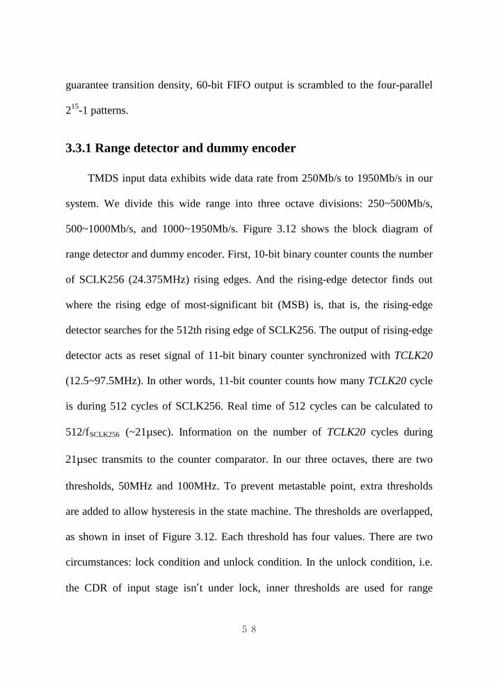
58
guarantee transition density, 60-bit FIFO output is scrambled to the four-parallel
215
3.3.1 Range detector and dummy encoder
-1 patterns.
TMDS input data exhibits wide data rate from 250Mb/s to 1950Mb/s in our
system. We divide this wide range into three octave divisions: 250~500Mb/s,
500~1000Mb/s, and 1000~1950Mb/s. Figure 3.12 shows the block diagram of
range detector and dummy encoder. First, 10-bit binary counter counts the number
of SCLK256 (24.375MHz) rising edges. And the rising-edge detector finds out
where the rising edge of most-significant bit (MSB) is, that is, the rising-edge
detector searches for the 512th rising edge of SCLK256. The output of rising-edge
detector acts as reset signal of 11-bit binary counter synchronized with TCLK20
(12.5~97.5MHz). In other words, 11-bit counter counts how many TCLK20 cycle
is during 512 cycles of SCLK256. Real time of 512 cycles can be calculated to
512/fSCLK256 (~21μsec). Information on the number of TCLK20 cycles during
21μsec transmits to the counter comparator. In our three octaves, there are two
thresholds, 50MHz and 100MHz. To prevent metastable point, extra thresholds
are added to allow hysteresis in the state machine. The thresholds are overlapped,
as shown in inset of Figure 3.12. Each threshold has four values. There are two
circumstances: lock condition and unlock condition. In the unlock condition, i.e.
the CDR of input stage isn’t under lock, inner thresholds are used for range

59
detection, and vice versa. Counter comparator already knows these threshold
values. Counter comparator judge the incoming 11 bits are larger or smaller than
each threshold values. Assume the incoming video resolution is XGA having 65-
MHz pixel clock under lock condition. In our notation, XGA has 32.5-MHz of
TCLK20. During 512 cycles of SCLK256, TCLK20 approximately has 683 cycles.
There are eight comparators for eight threshold values. Each threshold value
already knows each specific counter output. Counter value is easily calculated as
follows:
20256
512( ) TCLKSCLK
Counter value f(f )
= × (3.1)
For example, comparator for 50MHz, 51.2MHz, 100MHz, and 102.5MHz has 525,
538, 1050, and 1075 of counter value, respectively. Lower threshold determines
least-significant bit of range codes (Range<0>), while higher threshold determines
MSB (Range<1>). Through counter comparator and range detection, we get the
range codes (Range<1:0>). Simplified state machine is depicted in Figure 3.13.
The range codes also determine the patterns of 5-bit dummy data. According to
Range<1:0>, 10101, 01010, or 10110 patterns are selected. And these specific
patterns help the receiver recover the range codes.

60
3.3.2 Data aligner
In the CDRs and 1:20 DEMUXs of the input stage, three TMDS data are
parallelized to the three 20-bit wide data. These 60-bit data and three output
clocks of the CDRs have no phase relationship. Therefore data alignment is
necessary. Data aligner looks for rising edge of three output clocks of CDRs near
the alignment clock (Aligned TCLK20), as shown in Figure 3.14. TCLK20 from
the TMDS clock buffer experiences two delay circuits. Through two delays, three
TCLK20 clocks having different delay time are generated: TCLK20-Early, aligned
TCLK20, and TCLK20-Late. Rising-edge detector generates a divider reset signal
when all rising edges of three TCLK20 clocks are detected. This reset signal
makes the frequency dividers of the CDRs simultaneously restart. By using rising-
edge detector and divider reset all rising edges of three TCLK20 clocks are
between TCLK20-early and TCLK20-late, thus mid-delayed clock (aligned
TCLK20) is used for retiming clock of D flip flop (DFF).
3.3.3 Frequency domain conversion: FIFO, DAV generator, , header encoder, and scrambler
To realize the stationary-data-rate scheme, frequency domain conversion is
required from T-domain into S-domain. FIFO, DAV generator, and header
encoder perform the frequency domain conversion. Figure 3.15 shows the block
diagram of the FIFO, DAV generator, and header encoder. TCLK20 and SCLK64

61
are respectively used as write clock and read clock in the FIFO. To control the
FIFO, Gray-code counter and one-hot encoder are exploited. Truth table of the 6-
state Gray-code counter (GCC) and one-hot encoder (OHE) is depicted in Table
3.1.
First Gray-code counter (GCC-1) is operated with TCLK20, and generates 3-
bit 6-state Gray code (GCT<2:0>). This Gray code is one-hot-coded into 6-bit
write pointers (W<5:0>) that only one bit is high among six bits. Second Gray-
code counter (GCC-2) and one-hot encoder (OHE-2) have same operations except
data-valid signal (DAV) acts as enable signal. GCC-2 generates 6-bit read pointers
(R<5:0>) for the FIFO. The output of GCC1 is retimed with SCLK64 through
three DFFs and these Gray codes are also one-hot-encoded to write pointers
synchronized with SCLK64 (WS<5:0>). The write pointers and read pointers are
exploited as control signals of the FIFO units, and retimed write pointers and read
pointers are used for DAV generator. The DAV generator is simple digital logic
having following Boolean equation:
0 2 1 3 2 4 3 5 4 0 5 1DAV R WS R WS R WS
R WS R WS R WS= < > < > + < > < > + < > < >
+ < > < > + < > < > + < > + < > (3.2)
As we can see the equation, DAV is only high when R<5:0> and WS<5:0> have
specific combinations. Because R<5:0> and WS<5:0> are one-hot codes, there are
only six combinations that make DAV to be logic high as indicated in Table 3.2.

62
In the FIFO, there are 6 x 60 FIFO units. All data inputs (Din<59:0>) come into
DFFs with enable signals, write pointers (W<5:0>). Din<59:0> is consecutively
written to applicable FIFO unit by W<5:0>. Written data is loaded in the output of
DFF (Load<5:0>). And read pointers (R<5:0>) read the applicable data to the
FIFO output.
The write pointers are synchronized with T-domain clock, while the read
pointers are operated with S-domain clock. The read pointers also have
information on the DAV ratio. Detail timing diagram of this complicated
operations are depicted in Figure 3.16. Figure 3.16(a) is under conditions that
TCLK20 is 48.75MHz, i.e. DAV ratio is one half. In that figure, two write pointers
(W<5:0> and WS<5:0>) change in regular sequence irrespective of the DAV,
while the read pointers (R<5:0>) only change when previous DAV is high. In
other words, R<5:0> is fixed until DAV is high. And WS<5:0> continuously
change, and DAV goes to high when specific combinations are established. Figure
3.16(b) indicates the timing diagrams when DAV ratio is three-fifths. In the
timing diagrams, the output of FIFO (FIFOout<59:0>) has duplicate data. Sixty
selecting MUXs choose the data between FIFOout<59:0> and dummy data
according to the DAV. These S-domain 60-bit wide data is encoded to 215-1 PRBS
data by 4-parallel 15-wide scramblers. And 4-bit header is also generated
depending on the DAV. When DAV is high, 4-bit header is ‘1100’, and vice versa.

63
Finally, we get the 64-bit frame-based stationary-data-rate data which reflect the
TMDS data rate.
FIFO
1 0
60 60
DAV He
ader
Enco
der
Scra
mbl
er(1
5 x
4)60
4
6064
To 6
4:1
MUX
Sele
ctin
g M
UX (x
60)
Rang
eDe
tect
orDu
mm
yEn
code
r
TCLK
10
SCLK
64
Rang
e<1:
0>
Dum
my<
4:0>
x 1
2
Data
Alig
ner
Data
<59:
0>
Alig
ned
TCLK
20
Alig
ned
Data
<59:
0>
Divi
der
Rese
t
TCLK
203
2
Figure 3.11: Transmitter digital stage architecture
64
TCLK
10
10bi
tB
inar
y C
ount
er
SCLK
256
MSB
Res
et
DFF
Del
ayed
R
eset
11bi
tB
inar
y C
ount
erC
ount
erC
ompa
rato
r
50.0
MH
z50
.5M
Hz
50.7
MH
z51
.2M
Hz
100.
0MH
z10
1.0M
Hz
101.
5MH
z10
2.5M
Hz
Ran
ge-0
Ris
ing-
Edge
Det
ecto
r
Ran
geD
etec
tion R
ange
<1:0
>
12.5
~97.
5MH
z25
~195
MH
z
Ran
ge-1
Ran
ge-2
TCLK
10
Dum
my
Enco
der
00: 1
0101
01: 0
1010
1x: 1
0110
5
11
TMD
S D
ata
Rat
esR
ange
<1:0
>25
0 ~
500M
b/s
2b’0
050
0 ~
1000
Mb/
s2b
’01
1000
~ 1
950M
b/s
2b’1
x
50.0MHz 50.5MHz 50.7MHz 51.2MHz
100.0MHz 101.0MHz 101.5MHz 102.5MHz
%2
Thre
shol
d-1
Thre
shol
d-2
Figure 3.12: Range detector with dummy encoder

65
TCLK10 > 50MHz ?
TCLK10 < 51.2MHz ?
TCLK10 > 50.5MHz ?
TCLK10 < 50.7MHz ?
TCLK10 > 101MHz ?
TCLK10 < 101.5MHz ?
TCLK10 < 102.5MHz ?
YES
YES
Range<1:0>=2b’00
NO
YES
Range<1:0>=2b’01
TCLK10 > 100MHz ?NO
YES
Range<1:0>=2b’1x
NO Range<1:0>=2b’00
Range Detection Start
YES
YES
Range<1:0>=2b’00
NO
YES
Range<1:0>=2b’01
NO
YES
Range<1:0>=2b’1x
NO Range<1:0>=2b’00
LOCK ?
YES
NO
Figure 3.13: Simplified state machine for range detection

66
%2TCLK10
Delay Delay
TCLK20
TCLK20-Early
TCLK20-Late
DividerReset
DFFData<59:0> Aligned
Data<59:0>
Rising-EdgeDetector
Aligned TCLK20
3
Figure 3.14: Data aligner
Table 3.1 Truth table of gray-code counter and one hot encoder
6-State Gray Code Output <2:0>
(Binary / Decimal)
One Hot Encoder Output <5:0>
(Binary / Decimal) 000 / 0 001000 / 8 001 / 1 010000 / 16 011 / 3 100000 / 32 111 / 7 000001 / 1 110 / 6 000010 / 2 100 / 4 000100 / 4
Table 3.2 Combinations of R<5:0> and WS<5:0> for high DAV
R<5:0> (Binary / Decimal)
WS<5:0> (Binary / Decimal)
000001 / 1 000100 / 4 000010 / 2 001000 / 8 000100 / 4 010000 / 16 001000 / 8 100000 / 32 010000 / 16 000001 / 1 100000 / 32 000010 / 2

67
6-St
ate
Gra
y C
ode
Cou
nter
TCLK
20
Enab
le
One
Hot
Enco
der
6-St
ate
Gra
y C
ode
Cou
nter
SCLK
64
Enab
le
One
Hot
Enco
der
3 3
DFF (x3)
One
Hot
Enco
der
3
FIFO
uni
t6
x 60
Dat
aVa
lidG
ener
ator
66 6
W<5
:0>
R<5
:0>
Din
<59:
0>60
60 FIFO
out
<59:
0>
DA
V
GC
C1
GC
C2
DFF
60
Enab
leW
<0>
TCLK
20
NA
ND
2R
<0>
Din
<59:
0>
FIFO
uni
t<0>
(x60
)
DFF
60
Enab
leW
<5>
TCLK
20
NA
ND
2R
<5>
Din
<59:
0>
FIFO
uni
t<5>
(x60
)
NA
ND
6(x
60)
…
…
Dou
t<59
:0>
GC
T<2:
0>
GC
S<2:
0>
WS<
5:0>
Hea
der
Enco
der
1: 1
100
0: 0
011
0 1
12 x
Dum
my<
4:0>
60
4
Dou
t<63
:0>
Sele
ctin
g M
UX(
x60)
Load
<5>
Load
<0>
Figure 3.15: FIFO, header encoder, and DAV generator for frequency
domain conversion

68
R<5:0>
SCLK64(97.5MHz)
GCT<2:0>
W<5:0>
GCS<2:0>
TCLK20(48.75MHz)
WS<5:0>
DAV
4 8 8 16 16 32 32 1 1 2 2 4 4 8 8 16 16 32 32 1 1 2 2 4
Din<59:0>
Load<0>
Load<1>
Load<2>
Load<3>
Load<4>
Load<5>
1100
d1
0011
1100
d2
0011
1100
d3
0011
1100
d4
0011
1100
d5
0011
1100
d6
0011
1100
d7
0011
1100
d8
0011
d1
na1
na2
na4
na5
d2
d1
na1
na2
na5
d2
d1
d3
na1
na2
na1
na2
d2
d1
d3
d2
d1
d3
na2
d5
d6
d2
d1
d3
d5
d6
d2
d7
d3
d5
d6
d8
d7
d3
d5
d6
d8
d7
d9
d5
d6
d8
d7
d9
d5
d6
d8
d7
d9
d11
d12
d8
d7
d9
d11
FIFOout<59:0> na1 na1 na2 na2 d1 d1 d2 d2 d3 d3 d4 d4 d5 d5 d6 d6 d7 d7 d8 d8 d9 d9 d10 d10
0 1 3 7 6 4 0 1 3 7 6 4
8 16 32 1 2 4 8 16 32 1 2 4
6 6 4 4 0 0 1 1 3 3 7 7 6 6 4 4 0 0 1 1 3 3 7 7
2 2 4 4 8 8 16 16 32 32 1 1 2 2 4 4 8 8 16 16 32 32 1 1
0 1 0 1 0 1 0 1 0 1 0 1 0 1 0 1 0 1 0 1 0 1 0 1
d1 d2 d3 d4 d5 d6 d7 d8 d9 d10 d11 d12
na0 na0 na0 d4 d4 d4 d4 d4 d4 d10 d10 d10
0011
1100
d9
0011
1100
d10
0011
1100
na
0011
1100
na
0011
12
X
01010
12
X
01010
12
X
01010
12
X
01010
12
X
01010
12
X
01010
12
X
01010
12
X
01010
12
X
01010
12
X
01010
12
X
01010
12
X
01010
12
X
01010
MUXOutput<63:0>
(a)
R<5:0>
SCLK64(97.5MHz)
GCT<2:0>
W<5:0>
GCS<2:0>
TCLK20(58.5MHz)
WS<5:0>
DAV
4 8 8 16 32 32 1 1 2 4 4 8 8 16 32 32 1 1 2 4 4 8 8 16
Din<59:0>
Load<0>
Load<1>
Load<2>
Load<3>
Load<4>
Load<5>FIFOout<59:0> na1 na1 na2 na2 d1 d2 d2 d3 d3 d4 d5 d5 d6 d6 d7 d8 d8 d9 d9 d10 d11 d11 d12 d12
6 4 0 1 3 7 6 4 0 1 3 7 6 4
2 4 8 16 32 1 2 4 8 16 32 1 2 4
0 1 0 1 1 0 1 0 1 1 0 1 0 1 1 0 1 0 1 1 0 1 0 1
1100
na
0011
12
X
10110
8 16 32 1 2 4 8 16 32 1 2 4 8 16 32
0 1 3 7 6 4 0 1 3 7 6 4 0 1 3
d1 d2 d3 d4 d5 d6 d7 d8 d9 d10 d11 d12 d13 d14
na0 d4
d1
d2
d3
d5
d6
d7
d8
d9
d10
d11
d12
d13
d14
na0 na0
na1 na1 na1 na1
na2 na2 na2 na2 na2
na4
na5 na5
d1 d1 d1 d1 d1
d2 d2 d2 d2 d2
d3 d3 d3 d3 d3
d4 d4 d4 d4 d4
d5 d5 d5 d5 d5
d6 d6 d6 d6 d6
d7 d7 d7 d7 d7
d8 d8 d8 d8 d8
d9 d9 d9 d9 d9
d13
d12 d12
d11 d11 d11
d10 d10 d10 d10
1100
na
0011
1100
d1
12
X
10110
1100
d2
0011
12
X
10110
1100
d3
0011
1100
d4
12
X
10110
1100
d5
0011
12
X
10110
1100
d6
0011
1100
d7
12
X
10110
1100
d8
0011
12
X
10110
1100
d9
0011
1100
d10
12
X
10110
1100
d11
0011
12
X
10110
1100
d12
0011
12
X
10110
MUXOutput<63:0>
(b)
Figure 3.16: Timing diagram of frequency domain conversion (a) DAV ratio
= 1/2 and (b) DAV ratio = 3/5
69
3.4 Transmitter output stage
3.4.1 64:1 MUX with 6.24-GHz LC-PLL
The jitter performance of transmitter is influence on the system BER and the
sensitivity requirement of a receiver. The jitter performance of the serial data is
determined by S-domain. Therefore LC-type PLL is adopted in the transmitter
output stage. Block diagram of 64:1 MUX with 6.24-GHz LC-type PLL is shown
in Figure 3.17. 64:8 and 8:4 MUXs are realized with CMOS logic, while 4:1 high-
speed MUX uses CML logic. 64:8 MUX is implemented with shift-register
architecture for chip area reduction, while the other MUXs are based on tree
structure for power reduction. For testing 64:1 MUX with LC-PLL, 64-bit wide
parallel pseudo-random bit stream 27
-1 (PRBS7) generator is integrated in front of
64:8 MUX. By using enable signal, 64-bit parallel inputs are selected to the real
data streams (Din<63:0>) or PRBS7 data. In the PRBS7 testing mode, we can
easily verify the serial data is PRBS7 or not by measuring. The LC VCO has N-
core switching transistors. A center-tap spiral inductor (1.15nH) is used, and
locking range is from 6.05GHz to 6.45GHz with 1.4-V range of tuning voltage.
The gain of LC-VCO is ~286MHz/V.

70
3.4.2 Optical transmitter AFE: VCSEL driver
Stand-alone VCSEL driver conventionally consists of an input buffer for
electrical interface, a pre driver, and a main driver. The pre driver plays a role of
driving the large switching transistors of the main driver. However, we can omit
the input buffer and the pre driver. At the end of the 64:1 MUX, the CML buffer is
designed to have a sufficient driving capacity. Therefore by adding only the main
VCSEL driver, we can complete an optical AFE. To compensate physical
variations of the VCSEL due to temperature variations and aging effect, threshold
current (Ith) and modulation current (Imod) of VCSEL should be controlled [26].
External control bits for both currents are added for testing. Figure 3.18 shows a
block diagram of the main driver. The Ith and Imod can respectively be controlled
from 1mA to 2.5 mA and from 5mA to 20mA to meet the specification of
commercial VCSEL [27]. The commercial VCSEL is integrated on a printed-
circuit board for optical test.

71
PRB
S7G
ener
ator
64 64 Enab
le
6464
:8C
MO
S8
8:4
CM
OS
44:
1C
ML
CM
LB
uffe
r1
To V
CSE
LD
PFD
Up Dn
180u
A
180u
A
Vtun
eC
ML
Div
ider
%16
CM
OS
Div
ider
%16
%2
%2
SCLK
2SC
LK4
%2
SCLK
8
%2
SCLK
16
%4
SCLK
64To
dig
ital
proc
essi
ng
bloc
k
CLK
ref
24.3
75M
Hz
SCLK
256
LC V
CO
Din
<63:
0>
Cha
rge
Pum
p
6.24
-GH
z LC
-type
PLL
0 1
Figure 3.17: 64:1 MUX with 6.24-GHz LC-PLL

72
5mA
1mA
2mA
4mA
8mA
Mod
ulat
ion
Con
trol
M1
M2
VCSE
LD
umm
yVC
SEL
1mA
0.1m
A0.
2mA
0.4m
A0.
8mA
Thre
shol
d C
tl-1
Thre
shol
d C
tl-2
Two
Flas
h A
DC
s(E
NO
B :
4-bi
t)
4A
PC
AC
Info
.Fo
r Im
od
4
AM
CTop
Hol
d
Bot
tom
Hol
d
V TO
P
V BO
T
V AVG
Peak
Det
ecto
r
OPA
MP
DC
Info
.Fo
r Ith
DC
Ref
.
AC
Ref
.
PD
TIA
6.24
-Gb/
sSe
rial D
ata
1mA
0.1m
A0.
2mA
0.4m
A0.
8mA
Figure 3.18: VCSEL driver with auto-power and –modulation control

73
CHAPTER 4
SERIAL-LINK RECEIVER
4.1 Receiver structure
Figure 4.1 shows block diagrams of serial-link receiver. According to the
synchronized clocks and roles, it can be divided into three parts: receiver input
stage, receiver digital stage, and receiver output stage. First the receiver input
stage is synchronized with S-domain, and its vital roles are conversion an incident
optical signal into an electrical signal, extracting 6.24-GHz clock from the
incoming NRZ data, and parallelizing the 6.24-Gb/s NRZ data into 64-bit wide
data for next digital processing. Second, receiver digital stage fulfills the contrary
roles to the transmitter digital stage. It includes Barrel shifter, DAV decoder, de-
scrambler, range decoder, and FIFO. Unlike the transmitter, there is no T-domain
clock in the receiver. Based on information received by the transmitter, the
receiver should recover the T-domain clock. The digital stage extracts necessary
information from the incoming data, and deliveries it to receiver output stage.
Lastly, receiver output stage generates the T-domain clock and three TMDS data
by serializing. To make the T-domain clock from fractional DAV information, Δ-
Σ PLL is required.

74
PIN
PD
6.24
Gb/
sSe
rializ
ed D
ata
O/E
1:64
DEM
UX
with
CD
R
X-TA
L(2
3.37
5MH
z)
64B
arre
lSh
ifter
64
Sync
. M
onito
r
5
De-
Scra
mbl
er604
DA
VD
ecod
er
FIFO
60
Ran
geD
ecod
er5
2
CLK
64 (6
.25G
Hz/
64)
60
∆-Σ
Fra
ctio
nal
PLL
250~
1950
Mb/
sTM
DS
DA
TA (x
3)
25~1
95M
Hz
TMD
S C
lock
20:1
MU
X(x
3)
Dig
ital
Proc
essi
ng B
lock
Rec
eive
r inp
ut s
tage
Rec
eive
r dig
ital s
tage
Rec
eive
r out
put s
tage
On
Chi
pO
ff-C
hip
Figure 4.1: Three parts of the serial-link receiver
75
4.2 Receiver input stage
Receiver input stage consists of optical receiver AFE, LC-PLL-based dual-
loop CDR, and 1:64 DEMUX, as depicted in Figure 4.2. Optical receiver AFE
includes pre amplifier (trans-impedance amplifier, TIA) and post amplifier
(limiting amplifier, LMT). Optical receiver AFE converts the incoming 6.24-Gb/s
current signal into voltage signal having fixed swing. Dual-loop CDR extracts S-
domain clock from input data and retimes the input data with extracted clock. 1:64
DEMUX parallelizes 6.24-Gb/s data into 64-bit wide 97.5-Mb/s data.
4.2.1 Optical receiver analog front-end circuit
Figure 4.3 shows the optical receiver AFE circuit. Pre amplifier consists of a
regulated-cascode (RGC) current buffer, shunt-feedback trans-impedance stage
(TIS), and DC-offset-error cancellation buffer. The RGC buffer helps the effect of
an inherent PD junction capacitance from the bandwidth determination minimize
by providing very low input impedance [28]. The pre amplifier is designed with
consideration for a commercial GaAs-based p-i-n PD having 0.5-A/W
responsivity, 0.3-pF junction capacitance, and 8.5-Gb/s maximum data rate [29].
Conventional common-source differential pair is used for voltage amplifier of the
TIS with 2kΩ of feedback amplifier (RF). DC-offset-error cancellation buffer is
essential for a differential optical receiver to cancel DC-offset errors between
differential TIS outputs due to an inherent pseudo differential structure [30]. The
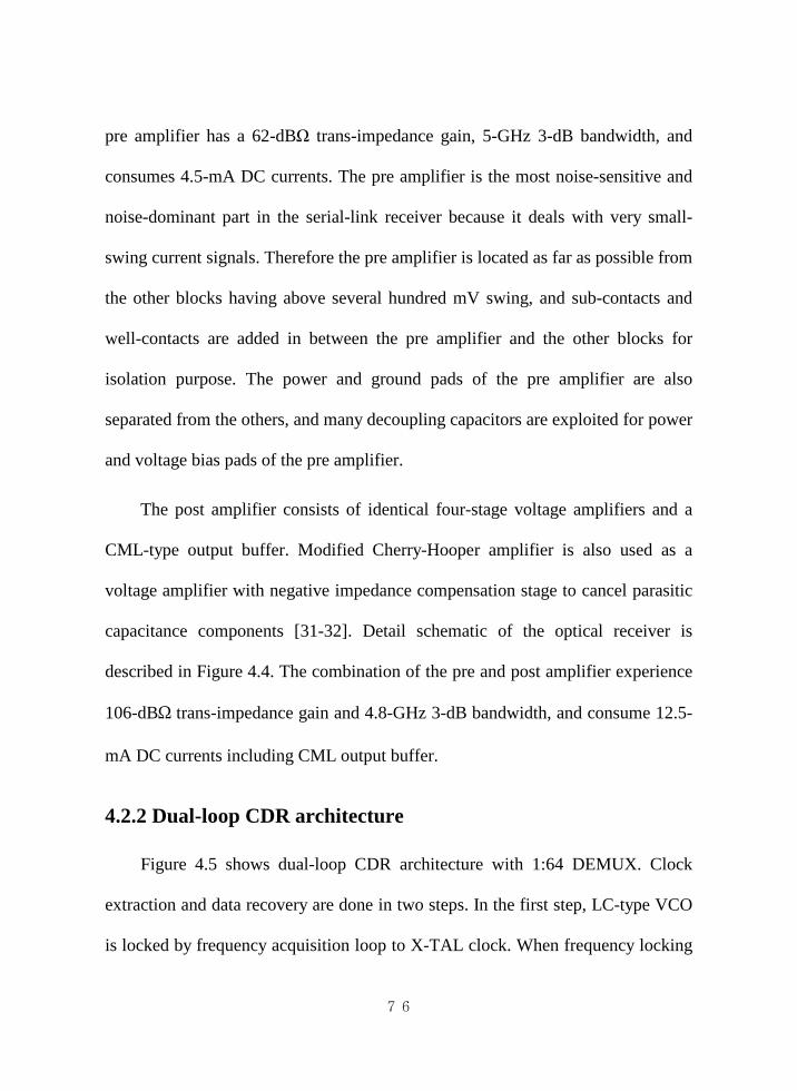
76
pre amplifier has a 62-dBΩ trans-impedance gain, 5-GHz 3-dB bandwidth, and
consumes 4.5-mA DC currents. The pre amplifier is the most noise-sensitive and
noise-dominant part in the serial-link receiver because it deals with very small-
swing current signals. Therefore the pre amplifier is located as far as possible from
the other blocks having above several hundred mV swing, and sub-contacts and
well-contacts are added in between the pre amplifier and the other blocks for
isolation purpose. The power and ground pads of the pre amplifier are also
separated from the others, and many decoupling capacitors are exploited for power
and voltage bias pads of the pre amplifier.
The post amplifier consists of identical four-stage voltage amplifiers and a
CML-type output buffer. Modified Cherry-Hooper amplifier is also used as a
voltage amplifier with negative impedance compensation stage to cancel parasitic
capacitance components [31-32]. Detail schematic of the optical receiver is
described in Figure 4.4. The combination of the pre and post amplifier experience
106-dBΩ trans-impedance gain and 4.8-GHz 3-dB bandwidth, and consume 12.5-
mA DC currents including CML output buffer.
4.2.2 Dual-loop CDR architecture
Figure 4.5 shows dual-loop CDR architecture with 1:64 DEMUX. Clock
extraction and data recovery are done in two steps. In the first step, LC-type VCO
is locked by frequency acquisition loop to X-TAL clock. When frequency locking

77
is done, lock detector generates lock signal (LOCK) which makes the phase
alignment loop be enable. With this, the VCO output (fOUT
Details of dual-loop CDR operation are described in Figure 4.6 and 4.7.
Figure 4.6 shows the frequency acquisition step. The phase-locked loop (PLL)
consists of phase-frequency detector (PFD), charge pump (CP), loop filter (LF),
LC-type VCO, and frequency dividers. The LD generates selecting signal of the
selecting MUX. Under unlock condition, the charge pump is controlled by the
output (Up and Dn) of the PFD. The phase alignment step is depicted in Figure 4.7.
When LOCK goes high, fast and slow BBPDs are enabled. The bang-bang phase
control is separated into two parts: proportional path and integral path [33]. The
fast bang-bang signals (EarlyF and LateF) of the proportional path directly control
a set of varactors inside LC-VCO with information on phase error polarity. The
) is aligned to the
optimum sampling point to the incoming NRZ data. The clock distributor
provides proper clock signals having desired frequency, driving capacity, and
swing levels to DEMUXs. De-multiplexing is also done in two steps, 1:4 first step
with CML and 4:64 second step with CMOS logic. To minimize power
consumption, CML is used only when necessary for high-speed blocks, while
other low-speed blocks use CMOS logic. High-speed 1:4 and 4:8 DEMUXs are
designed with the tree structure for power reduction while 4:64 DEMUX is based
on the shift-register architecture for chip area reduction. For testing purpose, a
PRBS error checker is embedded.

78
integral path is controlled by the slow bang-bang signals (EarlyS and LateS)
through the CP followed by a LF having two poles and one zero. The CDR has
loop bandwidth of 407kHz, phase margin of 61○
4.2.3 Samplers, DEMUXs, and bang-bang phase detector
, and closed-loop peaking of
1.32dB. By separating the bang-bang phase control path, the feedback-loop
latency can be reduced and the bandwidth requirements of the CP can be relaxed.
The amount of added RMS jitter generation due to the proportional path is
960fsec corresponding to the 6mUI-RMS. To prevent this jitter generation,
proportional control path can be substitute into a linear phase detector [34].
Through two parts of bang-bang phase control, the phase alignment loop tries to
align the rising edge of 4-phase clock to the optimal sampling point. To prevent
any interactions between the two loops, simultaneous operation doesn’t occur [35].
Figure 4.8 shows the block diagram of samplers with 1:2 DEMUX, 2:4 CML
DEMUX, 4:8 CMOS DEMUX, fast BBPD, and slow BBPD. Fast and slow
BBPDs are enabled by LOCK as mentioned above. 6.24-Gb/s serial data go
through three paths (A, B, and T) by three samplers and each path consists of three
sampling D-FFs with a delay buffer, sampling D-FFs or D latch (for path B), and
retiming D-FFs. In Figure 4.8, path A and B represent successive data streams
sampled at 0○ and 180○ of the clock phase. Path T samples an input data at the
transition timing between path A and B with 90○ of the clock phase. When two

79
sampled bits of path A and B have different polarities, path T can sense whether
the clock is early or late compared with data. If T3 equals to A3, the clock leads
the data and vice versa. The fast BBPD generates the maximum 3.12-GHz bang-
bang control signals (EarlyF and LateF) by comparing path A, path B, and path T
through exclusive OR (XOR) gates. To minimize the effect of a phase mismatch
between quadrature clocks, retiming D-FFs are used before the fast BBPD. The
samplers and fast bang-bang phase detector combined with 1:2 and 2:4 CML
DEMUX makes the chip area small, and makes a phase alignment between
proportional path and integral path unnecessary. A detailed timing diagram for
samplers and fast BBPD is described in Figure 4.9 for both fast and slow clock
conditions. Slow bang-bang signals (EarlyS and LateS) are generated by de-
multiplexing EarlyF and LateF through the bang-bang gating circuit. These slow
bang-bang signals control VCO through the charge pump and the loop filter.
Samplers, fast BBPD, 2:4 DEMUX, and divider operate on high-speed CML
signals and consume a large amount of currents. To reduce current consumption,
4:8 DEMUX and slow BBPD are designed with CMOS logic. A clocked sense
amplifier is used for efficient conversion from CML to CMOS logic, as shown in
Figure 4.10. The notations of each CML block in Figure 4.8, for example 1x, 2x,
and 4x, indicate the amount of tail currents compared with that in the basic CML
buffer, which consumes 0.15mA. The CMOS logic can process up to 1.56-Gb/s
data.

80
4.2.4 LC-VCO with 4-phase frequency divider
Figure 4.11 depicts LC-type N-core VCO with 4-phase frequency divider. A
center-tap spiral inductor (1.15nH) is used, and Miller capacitors are used as
variable capacitors, shown in inset of Figure 4.11. The variable capacitors are
controlled by two different control signals. One is a proportional control signal
(VtuneP<1:0>) from the fast BBPD, and the other is an integral control signal
(VtuneI) from the slow BBPD in the phase alignment loop or from the PFD
through the CP and the LF in the frequency acquisition loop. VtuneP<1:0> have
information only on the phase error polarity and rapidly changes with the data
frequency, while VtuneI has information on the accumulated phase error.
VtuneP<1:0> are digital signals with CML level where the low level is
represented by 1.2V and the high level by 1.8V. These proportional control signals
directly control variable capacitors. Consequently, the proportional path pushes
fast locking while the integral path makes it possible to achieve the accuracy.
A variable capacitance controlled by VtuneI is designed to be larger than one
controlled by VtuneP<1:0> by factor of 4 in order to reduce ripple voltages. The
proportional path has 208MHz/V of VCO gain and the integral path 1.095GHz/V.
The simulated frequency tuning range at different conditions of EarlyF/LateF and
VtuneI is depicted in Figure 4.12. The peak detector forces the output swing of
LC-VCO to equal the bandgap voltage (1.25V) by controlling tail currents, and its

81
schematic is depicted in Figure 4.13. LC-VCO output passes through 4-phase
frequency divider for half-rate bang-bang operation, shown in inset of Figure 4.11.
To confirm 1:64 DEMUX properly operates for 64-bit parallel output data,
the PRBS error checker is embedded and its schematic is shown in Figure 4.14.
The error checker can make a decision whether parallel 64-bit data are correct
PRBS7 data or not. In the experiment environment, we can easily judge the input
stage is clear by inputting PRBS7 signals into serial-link receiver.
1:64DEMUX
Dout<63:0>Pre/Post
Amp.
LC-PLL-based Dual-loop CDR
64
PINPD
X-TAL(24.375MHz)
SCLK64CX
Figure 4.2: Receiver input stage

82
RGCBuffer
iPDNRZ Optical Signal
MMF
DC-offsetCancel
GainStages
CX
CMLBuf.
ToSamplers
Pre Amplifier(TIA)
Post Amplifier (LMT)
PIN PD
RF
RF
TIS
Figure 4.3: Optical receiver analog front-end

83
M6
M6
M4
M4
M4
M4
RD
RD
RD
RD
Mod
ified
Che
rry-
Hoo
per
Am
plifi
er w
/ NIC
M5
M5
C
RF
RF
M1
M1
RFI
LT
CFI
LT
RFI
LT
CFI
LT
PDCX
V PD
M3
M3
M3
M3
M7
M7
Gai
n St
age
LPF
+ D
C-o
ffset
Can
cella
tion
Buf
fer
4-St
age
Lim
iting
Am
p. (M
odifi
ed C
herr
y-H
oope
r Am
plifi
er w
/ NIC
)C
ML
Buf
fer
Pre
Am
plifi
erPo
st A
mpl
ifier
MB
RB
M1
MB
RB
M1
Reg
ulat
ed-C
asco
de
Cur
rent
Buf
fer
i PDR
D
RD
RD
RD
RD
RD
Off-
Chi
p
PIN
PD
ToSa
mpl
ers
RD
RD
M6
M6
M4
M4
M4
M4
RD
RD
RD
RD
Mod
ified
Che
rry-
Hoo
per
Am
plifi
er w
/ NIC
M5
M5
C
Figure 4.4: Detail schematic of optical receiver AFE

84
1:4CML
DEMUX
4:64CMOS
DEMUX
1
0FrequencyAdjustment
Loop
PhaseAlignment
Loop
fREF
LockDetector
PRBSError
Checker
ClockDistrubutor
6.24GHz
LC VCO
NRZData
24.375MHzX-TAL
fOUT
VLOCK
Figure 4.5: Dual-loop CDR with 1:64 DEMUX

85
Samplers
FastBBPDwith
2:4 DEMUX
4-PhaseDivider
1/2
4-Phase Clock
LoopFilter
ChargePump
10
SlowBBPDwith
4:8 DEMUX
8:64DEMUX
Phase-Freq.
Detector
1/2 1/8
4 8 64 Built-inError
Checker
LockDetecter
1/4LC-VCO
Proportional Path
IntegralPath
EarlyF/LateF
ErrorIndication
Phase-Locked Loop
fOUT
fREFLOCK
VtuneI
VtuneP<1:0>
SCLK256Up/Dn
LOCK
SCLK641/2
64:1TestMUX Deserialized
Data
NRZ Data6.24 Gb/s
SelectMUX
LOCK
EarlyS/LateS
Figure 4.6: Frequency acquisition step of the dual-loop CDR
Proportional Path
Samplers
FastBBPDwith
2:4 DEMUX
4-Phase Clock
SlowBBPDwith
4:8 DEMUX
8:64DEMUX
4 8 64 Built-inError
Checker
IntegralPath
EarlyF/LateF UpS/DnS
VtuneP<1:0>
LOCK
LOCK
64:1TestMUX
4-PhaseDivider
1/2
LoopFilter
ChargePump
10 Phase-
Freq.Detector
1/2 1/8
1/4LC-VCO
Phase-Locked Loop
fOUT
fREFLOCK
VtuneI
SCLK256Up/Dn
SCLK641/2
NRZ Data6.24 Gb/s
SelectMUX
LockDetecter
ErrorIndication
Deserialized Data
Figure 4.7: Phase alignment step of the dual-loop CDR

86
CM
L1x
D-F
FC
ML1
x
D-F
FC
ML1
x
D-L
ATC
HC
ML1
x
D-F
FC
ML1
x
D-F
FC
ML1
x
D-F
FC
ML1
xD
-FF
CM
L2x
with
Buf
.
1:2
CM
L2x
1:2
CM
L2x
1/2
CM
L1x
BU
FFER
CM
L2x
BU
FFER
CM
L4x
Sam
pler
s
6.24
Gb/
sD
ATA
CLK
2 90
SCLK
4D
ivid
er
2:4
DEM
UX
CLK
2 270
Ret
imin
g D
-FFs
BU
FC
ML1
x
BU
FC
ML1
x
Early
F+
Late
F+
B AA
1
Fast
BB
PD
SCLK
2 0SC
LK2 1
80
SCLK
8
4:8
CM
OS
Dou
t<7:
0>
1/2
CM
OS
Sens
eA
mpl
ifier
with
FF
(x4)
Sens
eA
mpl
ifier
with
FF
(x4)
2:4
CM
L1x
CM
L1x
CM
L to
CM
OS
Early
-Lat
eG
atin
gEa
rlyS
Late
SEa
rly-L
ate
Gat
ing
Slow
BB
PD
4:8
DEM
UX
D-F
FC
ML2
xw
ith B
uf.
D-F
FC
ML2
xw
ith B
uf.
A2
A3
B1
B2
B3
TT 1
T 2
T 3
D-F
FC
ML1
x
D-F
FC
ML1
x
A1
= D
0B
1 =
D18
0T1
= D
90
A2
= D
0,0
B2
= D
180,
0T2
= D
90,9
0
A3
= D
0,0,
0B
3 =
D18
0,0,
0T3
= D
90,9
0,0
Early
F =
A3
+ T3
Late
F =
B3
+ T3
Early
F-
Late
F-
Figure 4.8: Samplers, fast BBPD, slow BBPD, and 1:8 DEMUX
87
CK0
CK90
CK180
CK270
0 1 2 3 4 5 6 7
1 3
1 3
1 3 5
1 3 5
1 3 5
1 3
0 2 4 6
0 2 4
0 2
A1
A2
A3
B1
B2
B3
C1
C2
C3
DATA
+ +EarlyFNo Signal
LateFRandomSignal
Optimal Sampling
Point
(a)
CK0
CK90
CK180
CK270
0 1 2 3 4 5 6 7
0 2
0 2
0 2 4
1 3 5
1 3 5
1 3
0 2 4 6
0 2 4
0 2
A1
A2
A3
B1
B2
B3
C1
C2
C3
DATA
+ +EarlyFRandom Signal
LateFNo
Signal
Optimal Sampling
Point
(b)
Figure 4.9: Timing diagram of fast bang-bang signals when (a) clock leads
data and (b) clock lags data

88
CLKIN
PIN
M
x2x4
x2x4
SR-
Latc
hD
-FF
x6O
UT
M1
M2
M3
M4
M6
M5
M7M
8M
9
M10
M11
M12
Figure 4.10: Clocked sense amplifier

89
Peak
Det
ecto
rD
-LA
TCH
CM
L 1x
D-L
ATC
HC
ML
1x
CM
LVC
O B
uffe
r
CM
LVC
O B
uffe
rC
K27
0
CK
90
CK
180
CK
0
4-Ph
ase
Freq
. Div
ider
M4
M3
M2
M1 C
ente
r-ta
p Sp
iral I
nduc
tor V t
uneP
<1:0
>
V tun
eI
M8
M7
M5
M6
VCO
OU
TPVC
OO
UTM
V tun
e
Varia
ble
Cap
acito
r U
nit
4x1x Vara
ctor
s
VCO
OU
TMVC
OO
UTP
VB1
VB2
Figure 4.11: LC-type VCO with 4-phase frequency divider

90
Figure 4.12: LC-type VCO tuning range

91
OPA
MP
V BG
VB2
VB1
VCO
OU
TMVC
OO
UTP
V BIA
S
Tail
Cur
rent
Bia
sing
M9
M10
M11
M12
M13
M14
M15
M16
M17
M18
M19
M20
M22M21
M23
C1
C2
Figure 4.13: Peak detector to maintain VCO output swing

92
DINx<19:7>DINx<18:6>DINx<12:0>
XNOR3NOR3
NOR3
NOR3
NOR3
NAND2Enable
DIN<19:0> DINx<19:0>
XORout<12:0>XORout<1>XORout<2>XORout<8>
XORout<7>XORout<6>XORout<0>
XORout<10>XORout<9>XORout<3>
XORout<4>XORout<5>
XORout<11>
XORout<12>
CLK
D-FF Error
20-bit wide PRBS7 Error Checker
NAND5
Enable
DIN<19:0>
SCLK64
DIN<23:4>
DIN<43:24>
DIN<63:44>
20b-wideError
Checker
20b-wideError
Checker
20b-wideError
Checker
20b-wideError
Checker
D-FF Error
NOR2
NOR2
NAND2
Figure 4.14: PRBS7 error checker
93
4.3 Receiver digital stage
Main roles of a receiver digital stage are aligning 64-bit parallel sequence,
extracting information on T-domain clock from 4-bit header and dummy patterns,
transmitting this information to the receiver output stage, and converting S-
domain into T-domain by using recovered T-domain clock by fractional PLL. The
digital stage consists of Barrel shifter, DAV decoder, range decoder, de-scrambler,
and FIFO, as shown in Figure 4.15.
The 64-bit parallel data from the receiver input stage can have any one of 64
possible starting locations. To read the range information from the data and to
align three TMDS channels, Barrel shifter with synchronization monitor is
exploited. DAV decoder recovers DAV signal same to the transmitter side from 4-
bit header. Except for header, 60-bit data is again de-scrambled. With recovering
DAV signal and dummy patterns when DAV signal is logic 0, range decoder
extracts range codes equal to the transmitter side. This range information becomes
a reference on T-domain clock. The FIFO reads the 60-bit data with S-domain
clock and writes with T-domain clock. The FIFO also generates current ratio
between S-domain clock and T-domain clock, and transmits this information to
the fractional PLL. This information determines frequency dividing factor of the
delta-sigma modulator in the fractional PLL.

94
4.3.1 Barrel shifter with synchronization monitor
The receiver input stage parallelizes 6.24-Gb/s serial data into 64-bit 97.5-
Mb/s data. In this process serial data is randomly sampled, thus any bit can be first
bit of frame. In the all serial-link systems, channel alignment is always issue.
Conceptual timing diagram of channel alignment is depicted in Figure 4.16. In the
transmitter side, we add 4-bit header in front of 60-bit data frame. 4-bit header has
two kinds of simple sequence: 1100 for real frame or 0011 for dummy frame. 60
bits except for header were now scrambled. Therefore if we look for header and
we check the repetitive header indicates every frame during eight cycles, we have
confidence that the channels are aligned. Synchronization monitor (sync. monitor)
looks at 4-bit header. If 4-bit header once matches, the monitor checks the header
every frame. If the header matches to known value during eight clocks,
synchronization signal (SYNC) goes to high. To align the frame by rotating 64-bit
data, shifting range from 0 bit to 63 bits is required. In order to shift by up to 63
bits, the current 64 bits word and the previous 63 bits are needed. Therefore the
monitor generates 6-bit shift signals (SFT<5:0>) for 63-bit shifting. 6-stage
shifter either shifts by 2N or the data goes straight, i.e. SFT<N> signal determines
relating stage shifts the data by 2N or no shift. Among 127 bits (current 64 bits +
previous 63 bits) the monitor searches for the location of header, as described in
Figure 4.17.

95
4.3.2 DAV decoder, de-scrambler, range decoder, and FIFO
In the receiver side, there is no T-domain clock. However, information on T-
domain clock is in the input data. By aligning 64-bit parallel data, we can easily
check the header and decide this frame is real or dummy. The 4-bit header is
encoded in the transmitter to 1100 for real frame or 0011 for dummy frame. With
this pattern difference, DAV decoder simply generates DAV signal same to the
one of the transmitter. And this DAV signal is very crucial information for
synthesizing TMDS clock. As previously explained in the Chapter 3, DAV signal
indicates the ratio of TCLK20 to SCLK64. Through the de-scrambler, aligned 60-
bit data becomes original data. In the dummy frame, i.e. DAV is logic 0, specific
dummy patterns appear according to the range codes. By checking already known
dummy patterns, the range codes (Range<1:0>) can be recovered. Simple
diagram for DAV decoder, de-scrambler, and range decoder is shown in Figure
4.18.
The asynchronous receiver FIFO is used to convert S-domain data into T-
domain data in common with the transmitter FIFO. In the receiver FIFO,
situations are different compared with the transmitter FIFO. In the transmitter, T-
domain and S-domain clocks are defined from the TMDS input clock and X-TAL
reference clock. However, there is no T-domain clock above mentioned. With
DAV signal and range codes, we ought to recover the TMDS clock. Figure 4.19
96
depicts the receiver FIFO. The write clock comes from the receiver input stage
and is always 97.5MHz (SCLK64). The read clock should be TCLK20 and is
synthesized by the fractional PLL. The DAV acts as an enable signal of write
operation. Before the output PLL finds the correct T-domain clock, the read
operation cannot work properly. The FIFOfill indicates whether the FIFO is filled
more or less than half full. The FIFOfill provides phase and frequency information
for the T-domain clock synthesis. The receiver FIFO organizationally operates
with delta-sigma modulator and fractional PLL of the receiver output stage. The
operations of the FIFO will be treated in more detail in the next section.

97
Bar
rel
Shift
er
Dat
a<63
:0>
SCLK
64
Sync
. M
onito
r
5
Alig
ned
Dat
a<59
:0>
Hea
der<
3:0>
De-
Scra
mbl
er(1
5 x
4)
DA
V D
ecod
er
Dat
a<59
:0>
DA
VR
ange
Dec
oder
Ran
ge<1
:0>
FIFO
Rea
d C
lock
2
Writ
e C
lock
(TC
LK20
)
FIFO
fill
From
Δ-Σ
PLL
To Δ
-Σ P
LL
To Δ
-Σ P
LL
Sync
Figure 4.15: Receiver digital stage

98
Rea
l(1
100)
Dum
my
(001
1)D
umm
y(0
011)
Dum
my
(001
1)
Rea
l(1
100)
Dum
my
(001
1)D
umm
y(0
011)
Dum
my
(001
1)
Bar
rel S
hifte
r
Dat
a fr
omin
put s
tage
DA
V si
gnal
Alig
ned
Dat
a<59
:0>
Sync
. Mon
itor
SYN
C =
1
SYN
C =
0
SYN
C =
0 Eigh
t goo
d fr
ames
One
bad
fr
ame
Figure 4.16: Conceptual timing diagram and state diagram of the Barrel
shifter

99
Cur
rent
64-
bit w
ord
Prev
ious
63-
bit w
ord
27-b
its s
hifti
ng64
bits
SFT<
5:0>
= 0
1101
1
head
erhe
ader
SYN
C
Stag
e 0
Stag
e 5
Stag
e 4
Stag
e 3
Stag
e 2
Stag
e 1
SFT<0>
Sync
. mon
itor
SFT<5>
SFT<4>
SFT<3>
SFT<2>
SFT<1>
Shift
by
(32,
0)Sh
ift b
y(1
6,0)
Shift
by
(8,0
)Sh
ift b
y(4
,0)
Shift
by
(2,0
)Sh
ift b
y(1
,0)
Cur
rent
64-
bit w
ord
Prev
ious
63-
bit w
ord
43-b
its s
hifti
ng64
bits
SFT<
5:0>
= 1
0101
1
head
erhe
ader
Cur
rent
64-
bit w
ord
Prev
ious
63-
bit w
ord
50-b
its s
hifti
ng64
bits
SFT<
5:0>
= 1
1001
0
head
erhe
ader
Figure 4.17: 6-bit shift signals according to the location of header

100
DA
V R
OM
“110
0”
Hea
der<
3:0>
4XO
R2
(x4)
4A
ND
4
De-
Scra
mbl
er4
x 15
60D
ata
DFF
DA
V
Dum
my
RO
M
1010
1: 0
001
010:
01
1011
0: 1
x
SCLK
64
602
Ran
ge<1
:0>
Figure 4.18: Block diagram for recovery of DAV and range codes

101
FIFOin<59:0> FIFOout<59:0>
FIFO6 x 60
W<5
:0>
R<5
:0>
FIFOController
SCLK64 TCLK20
Write CLK Read CLK
DAV FIFOfill
Figure 4.19: Simplified receiver FIFO

102
4.4 Receiver output stage
Main roles of the receiver output stage are synthesizing the TMDS clock with
the FIFO of the digital stage and serializing the 60-bit wide data into three TMDS
data with recovered TMDS clock. The output stage includes real and dummy
fractional PLL with Δ-Σ modulator (DSM), three 60:3 MUX, PRBS7 generator,
and TMDS output buffer.
Figure 4.20 describes the block diagram of the receiver output stage with the
FIFO. The FIFO controller generates FIFOfill signal which indicates whether the
FIFO is filled more or less than half full by comparing read and write clock. And
the FIFOfill controls the DSM and determines a fractional dividing factor of the
PLL. The PLL frequencies are adjusted by means of the feedback dividing factor.
The output clock of the PLL is again fed back to the FIFO as the read clock. This
feedback loop is divided into two different paths. By adding the dummy FIFO
controller and the dummy fractional PLL, fast locking and jitter reduction due to
dithering can be achieved.
First is the dummy loop. The dummy FIFO controller compares SCLK64
(write clock) with the output of dummy fractional PLL and generates dummy
FIFOfill (DFIFOfill). Through the DSM, fractional dividing factor for the dummy
PLL is determined from six control bits (DFDIV<5:0>). The dummy dividing
factor affects the output of the dummy PLL (DTCLK20) as well as the real DSM

103
through the digital low-pass filter (LPF). The DFIFOfill also controls a phase
rotator. Through the phase rotator, the dummy DSM loop has high slew rate.
Besides the charge pump current (8μA) of the dummy PLL is larger than that
(1μA) of the real PLL. Therefore the DTCLK20, the DFIFOfill, and the dummy
dividing factor can be changed quickly. The purpose of the dummy loop is to find
the nominal dividing factor for the real PLL. The dummy loop cannot be used for
the TMDS clock synthesis directly due to large hunting jitters. The phase rotating
divider is implemented with a divide by 19 or 21. This produces jitter of ±1UI
instantly.
Second, the real loop directly affects the TMDS clock. The dummy dividing
factor provides the nominal value of the real dividing factor through digital LPF.
The real loop unlike dummy loop has slow slew rate, therefore the DSM
effectively acts as a slow phase rotator. The FIFOfill either adds or subtracts a
small amount to the dummy dividing factor. This causes the frequency to be
higher or lower by a small amount corresponding to the small jitter. The
conceptual timing diagram for the FIFOfill, frequency of the TCLK20, and phase
of the TCLK20 is depicted in Figure 4.21 compared with the dummy PLL.
Second-order DSM which is used to control the fractional dividing factor of
the PLL is described in Figure 4.22. The input is N-integer bits and M-fractional
bits, corresponding to N-fractional bits of the output. Currently 18 fractional bits

104
and 6 integer bits are used. This allows for the frequency to be set to 1 part in 262
thousand. The first integrator has no delay and the second is vice versa. Each
integrator is depicted in Figure 4.22 as insets. The non-delayed integrator is
similar to the delayed-integrator but with the DFF in the feedback path. The
adders, for this design, are all N+M bits (24 bits) and are implemented in the
carry-bypass style. The quantizer simply consists of taking the N integer bits and
discarding the M fractional bits. Figure 4.23 shows the plot with respect to fast
Fourier transform of the DSM output. It can be seen that the phase noise rises at
40dB/decade and has a high pass response. This is due to the double integration
architecture. The result does not contribute significantly to the total phase noise
because the DSM noise is filtered by the low-pass response of the PLL.
Figure 4.24 shows the two fractional PLLs. The differences between them are
the existence of the phase rotator and the charge pump current. Feedback divider
(FB-DIV) is controlled by the DSM from 16 to 63 of fractional dividing factor.
The SCLK128 having 48.75-MHz frequency is used for a reference clock. Post
frequency dividing factor (PDIV) is controlled by the range codes according to the
frequency range of the input data. In the case of the UXGA resolution, TCLK10
has 162-MHz frequency and the dividing factor of the post divider is fixed to 1.
Therefore the fractional dividing factor is about 33.2. The fractional dividing
factor (FDIV) can be simply calculated as follows:
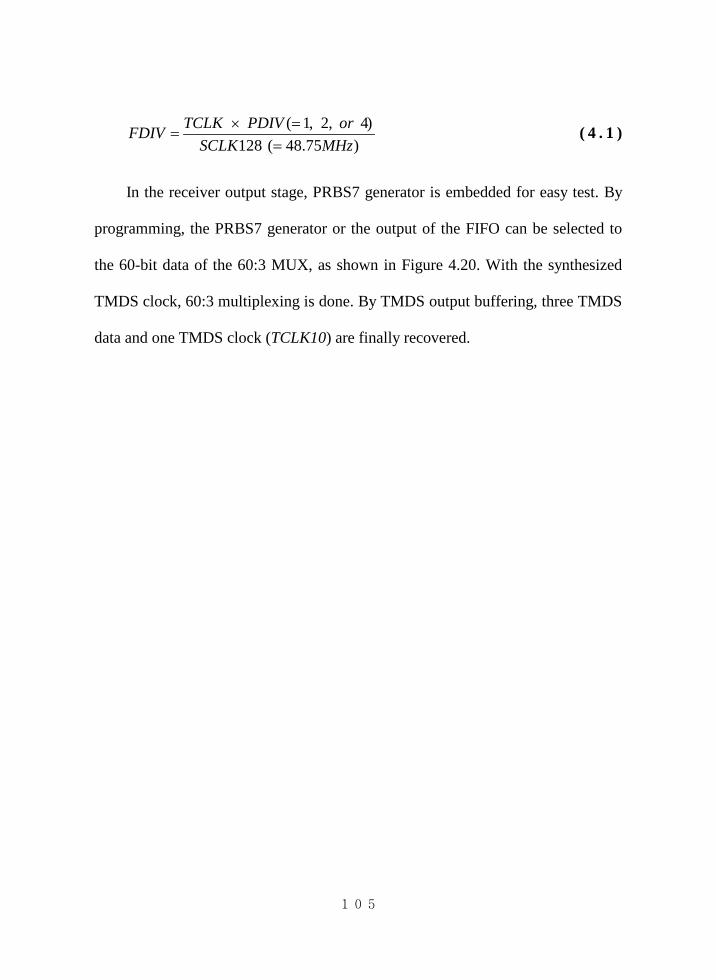
105
( 1, 2, 4)128 ( 48.75 )
TCLK PDIV orFDIVSCLK MHz
× ==
= ( 4 . 1 )
In the receiver output stage, PRBS7 generator is embedded for easy test. By
programming, the PRBS7 generator or the output of the FIFO can be selected to
the 60-bit data of the 60:3 MUX, as shown in Figure 4.20. With the synthesized
TMDS clock, 60:3 multiplexing is done. By TMDS output buffering, three TMDS
data and one TMDS clock (TCLK10) are finally recovered.

106
FIFO
in<5
9:0>
FIFO
out<
59:0
>
FIFO
6 x
60 W<5:0>
R<5:0> Rea
lFI
FOC
ontr
olle
rSC
LK64
TCLK
20W
rite
Rea
d
DA
VFI
FOfil
l
Dum
my
FIFO
Con
trol
ler
DTC
LK20
DFI
FOfil
l
Writ
e R
ead
Dum
my
24bi
t DSM
Rea
lFr
ac. P
LL
Dum
my
Frac
. PLL
DFD
IV<5
:0>
Phas
e R
otat
ing
Div
ider
%19
/21
Dig
ital
LPF
Rea
l24
bit D
SMA
dder
FDIV
<5:0
>
Ran
ge<1
:0>
60:3
MU
Xw
/ TM
DS
Buf
fer
DA
TA2
DA
TA1
DA
TA0
PRB
S7G
ener
ator
0 160
60
Prog
ram
min
g
Rec
eive
r out
put s
tage
%2
%10
TCLK
10
Figure 4.20: Receiver output stage with the FIFO

107
FIFOfill
Freq. (TCLK20)
Phase (TCLK20)
DFIFOfill
Phase (DTCLK20)
(a)
(b)
Figure 4.21: Conceptual plot for (a) the real DSM loop and (b) the dummy
DSM loop

108
Inte
grat
orw
ithou
t del
ayIn
tegr
ator
with
del
ay+
N-b
it +
M-b
it
+Q
uant
izer
__
DFF
+
N-b
it
N+M
N+M
CLK
DFF
+N
+M
N+M
CLK
Figure 4.22: Second-order Δ-Σ modulator

109
Figure 4.23: FFT of the DSM output
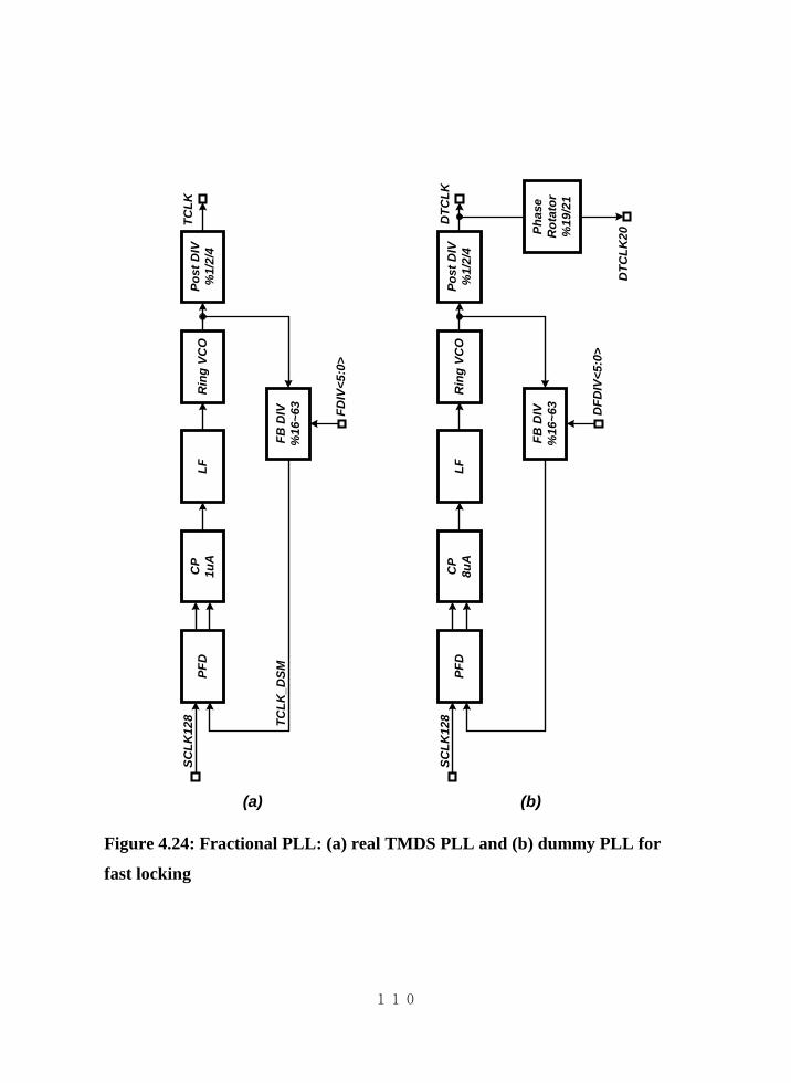
110
PFD
CP
1uA
LFR
ing
VCO
Post
DIV
%1/
2/4
FB D
IV%
16~6
3
SCLK
128
TCLK
FDIV
<5:0
>
TCLK
_DSM PF
DC
P8u
ALF
Rin
g VC
OPo
st D
IV%
1/2/
4
FB D
IV%
16~6
3
SCLK
128
DTC
LK
DFD
IV<5
:0>
Phas
e R
otat
or%
19/2
1
DTC
LK20
(a) (b)
Figure 4.24: Fractional PLL: (a) real TMDS PLL and (b) dummy PLL for
fast locking

111
CHAPTER 5
IMPLEMENTATION AND EXPERIMENT
RESULTS
5.1 Implementation
Serial-link transmitter and receiver with optical AFEs for display
interconnects are realized using a 0.18-μm standard CMOS technology. For
testing purpose, a test chip for the receiver input stage including optical receiver
AFE, 1:64 DEMUX, and dual-loop 6.24-Gb/s CDR is separately implemented
using same technology. Figure 5.1 shows the layout and microphotography of the
test chip. Serial-link transmitter and receiver chips are mounted on printed-circuit-
boards (PCBs), while the test chip for receiver input stage is measured in probe
station. Figure 5.2 and 5.3 respectively shows the layout and microphotography of
the serial-link transmitter and receiver. All bonding pads are protected by electro-
static discharge (ESD) protection diodes. The transmitter and receiver chips
occupy the area of 1.75mm × 1.97mm and 1.75mm × 2.08mm including ESD
protection diodes, respectively. High-speed in/out nodes more than 1Gb/s exploits
special pads made of only top metal to reduce parasitic capacitance (under 0.5pF),

112
while another pads exploits normal pads including all metals to provide efficient
current density.
Figure 5.1: Layout and microphotography of test chip for the receiver input
stage
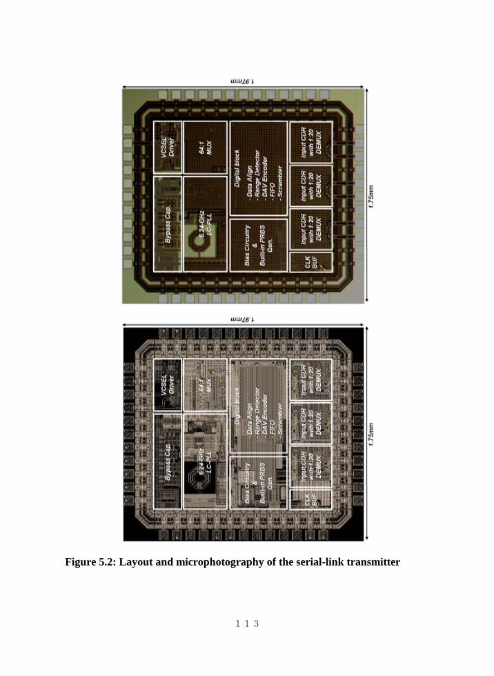
113
Figure 5.2: Layout and microphotography of the serial-link transmitter

114
Figure 5.3: Layout and microphotography of the serial-link receiver

115
5.2 Experiment results
5.2.1 Built-in testing circuitries
To realize stationary-data-rate scheme, serial-link transmitter and receiver
include very complex digital processing blocks. Therefore there are a lot of testing
points for both analog and digital signals. Analog test buses (ATEST) for
checking DC voltages, such as regulated 1.8-V core supply, bias voltages, and
VCO tuning voltages, are designed according to Figure 5.4. A 10-kΩ resistor is
included for ESD protection and to isolate the sensitive analog nodes being tested
from external noise. For testing digital signals, the transmitter and receiver are
programmed using a three wire serial data interface. The three pins are needed to
program the chips: SDLOAD (serial data load), SDIN (serial data in), and SDCLK
(serial data clock). The three pins drive a simple double buffered shift register. A
simplified diagram of the shift register is given in Figure 5.5. In order to program
the shift register, the data bits to be programmed using C++ language are driven
onto the SDIN and clocked in one at a time by rising edges of the SDCLK. Once
all of the necessary data is clocked into position in the bottom row of the shift
register, the data is loaded by asserting a rising edge of the SDLOAD. The shift
register is 64-bits long on the each chip. The timing diagram for three
programming pins is shown in an inset of Figure 5.5. The programming register
can be disabled when the three pins are all equal to logic high. This feature makes

116
disabling the programming of the DUTs (devices under test). Digital test buses
can measure the digital signals below 100-Mb/s data rate. Therefore we can
observe important signals influencing on the whole operations, such as TCLK20,
range codes, DAV signal, output of lock detector, built-in PRBS error, SCLK64,
and so on. Figure 5.6 and 5.7 show the graphic user interface (GUI) using C++
language and the simulation results of the programming pins. By simply clicking a
check box, we can measure the relevant node. The interface between computer
and the DUTs consists of a simple parallel port.
To easily confirm serial-to-parallel and parallel-to-serial operations in the
serial-link transmitter and receiver, PRBS7 generator and error checker is
embedded in the chips. For testing the transmitter input stage, three PRBS7 error
checkers are included. By inputting PRBS7 signal from pattern generator
instrument with clock divided by 10 to each TMDS data, each three 20-bit wide
data is checked whether PRBS7 is or not. And the results are observed in the
digital test bus (DTEST). For testing the transmitter output stage, 64-bit parallel
PRBS7 generator is designed. By controlling to the DTEST, the transmitter output
stage can select real 64-bit data or PRBS7 data as inputs. The serial output is
easily judged if PRBS7 is or not in the oscilloscope. The receiver input stage and
output stage are checked, along with the transmitter as described in Figure 5.8.

117
ATEST
10KΩVtest0
Vtest1
Vtest2
Vtest3
Figure 5.4: Analog test bus (ATEST)

118
DFF
DQ
D[0]
DFF
DQ
DFF
DQ
D[1]
DFF
DQ
DFF
DQ
D[2]
DFF
DQ
DFF
DQ
D[N-
1]
DFF
DQ
DFF
DQ
D[N]
DFF
DQ
……
…
……
…
SDLO
AD
SDIN
SDCL
K
D[63
]D[
62]
D[61
]D[
1]…
…D[
0]SD
IN
SDCL
K
SDLO
AD
……
D[60
]D[
59]
D[58
]D[
57]
Figure 5.5:Built-in programming register and its timing diagram
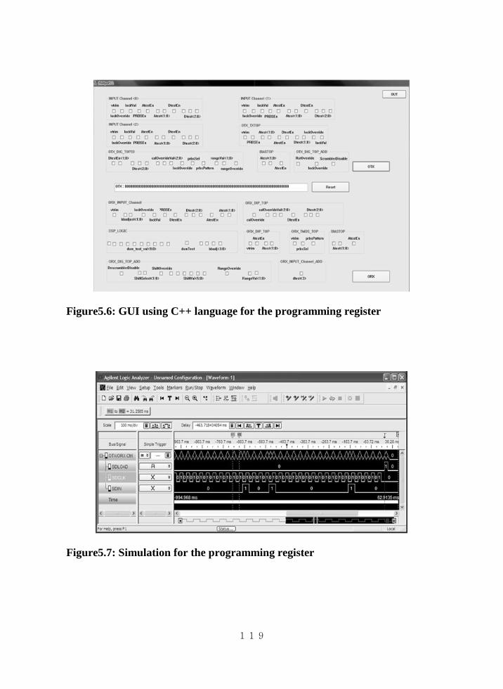
119
Figure5.6: GUI using C++ language for the programming register
Figure5.7: Simulation for the programming register

120
Opt
ical
Rx
&1:
64 D
EMU
Xw
/ CD
R
Dig
ital
Stag
e60
:3 M
UX
w/ P
LL
1
Seria
l D
ata
6460
PRB
S7C
heck
264
PRB
S7G
en2
60
DTE
ST
Dig
ital
Stag
e
64:1
MU
Xw
/ PLL
&O
ptic
al T
x
6064
1
Seria
l D
ata
60PR
BS7
Che
ck1 PR
BS7
Gen
164
1:20
DEM
UX
w/ C
DR
(x3)
DTE
ST
PRB
S7Pa
ttern
gene
rato
r
Clo
ck
Dat
a2
Dat
a1
Dat
a0
Osc
illos
cope
Clo
ck
Dat
a2
Dat
a1
Dat
a0
Osc
illos
cope
PRB
S7Pa
ttern
gene
rato
r
Seria
l-lin
k re
ceiv
er
Seria
l-lin
k tr
ansm
itter
Figure 5.8: Built-in PRBS generator and checker for testing serial-to-parallel
and parallel-to-serial operations

121
5.2.2 Measurement of the receiver input stage
The receiver input stage including optical receiver AFE, LC-PLL-based dual-
loop CDR, and 1:64 DEMUX is separately implemented to ensure operations of
the optical interface. Above and beyond test points on analog and digital test bus,
there are high-speed test points required additional output buffers. In the test chip
for receiver input stage, three testing points are added: behind optical receiver for
sensitivity and BER test, one of the 4-phase recovered clocks, and behind high-
speed 1:4 DEMUX having 1.56-Gb/s data rate, as shown in Figure 5.9.
Figure 5.10 shows the measurement setup for the receiver input stage. As
explained in Figure 5.9, the test chip has three additional high-speed test points:
the output of optical receiver AFE (TP-1), 4-phase output clock of the CDR (TP-
2), and the output of 1:4 DEMUX (TP-3). The fabricated chip was integrated with
a commercial 850-nm GaAs PIN PD on a PCB. The PD has 7.5-GHz bandwidth,
0.5-A/W responsivity, and 0.3-pF junction capacitance according to its data sheet.
A pulse-pattern generator (PPG) created PRBS7 for the on-chip error checker and
PRBS31 for other measurements. For optical measurement, a commercial 850-nm
VCSEL driver module and multi-mode fiber are used. An optical attenuator is
used for the optical sensitivity measurement. Measured S21 at TP-1, depicted in
Figure 5.11, exhibits 4.8-GHz bandwidth with 2-dB peaking at around 1.6GHz
which results from the modified Cherry-Hooper amplifier of the post amplifier.

122
Measured bandwidth indicates 77% of target bit rate, therefore the optical receiver
is located at near optimal points in terms of noise performance. Measured eye
diagram at TP-1 is shown in Figure 5.12 as an inset. 6.25-Gb/s eye diagram
exhibits 5-psec root-mean-square (RMS) jitter and 30-psec peak-to-peak (p-p)
jitter with differential 400-mVpp output swing, corresponding to the horizontal
eye opening of more than 0.8 UI. Figure 5.12 shows measured BER at different
incident optical power. Optical sensitivities for 1e-9 and 1e-12 BERs are
measured to -19.4dBm and -18dBm, respectively at 6.25-Gb/s data rate. Used
MMF having 62.5-μm core diameter has about 2.9dB/km of transmission loss.
Assuming 4-dB of coupling and insertion loss and -4-dBm of VCSEL output
power, ~3.9-km transmission distance is expected for 1e-9 BER. Of course this
distance is calculated without secondary dispersion effects of the MMF. Therefore
real distance can be reduced. Figure 5.13 shows the output of half-rate recovered
clock at TP-2 and the eye diagram of the 1:4 parallelized data at TP-3. The half-
rate 3.125-GHz clock of the CDR has 1.4-psec RMS jitter and 8.4-psec p-p jitter.

123
6.24Gb/s
MMF
TIALA
TP-1
PD1:4
CMLDEMUX
4:64CMOS
DEMUX4
Dual-loop CDR
64 Built-inError
CheckerError
Indication
64:1TestMUX
Deserialized Data
4-Phase Clock TP-2
TP-3
24.375MHzX-TAL
DUT (receiver input stage)
Figure 5.9: Additional testing points for the receiver input stage
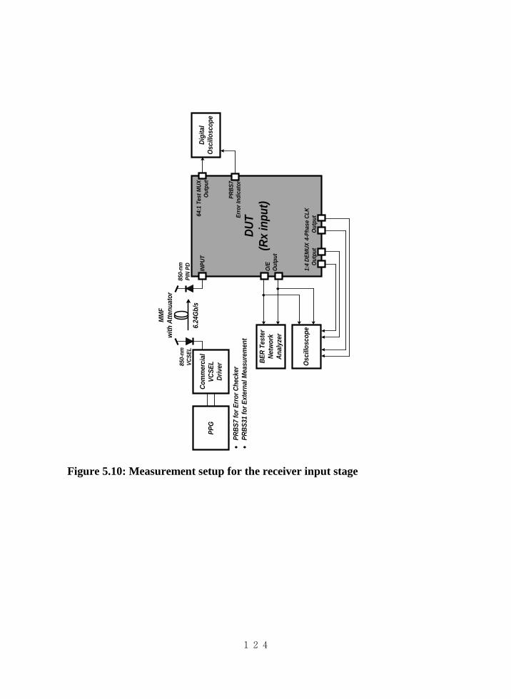
124
DUT
(Rx
inpu
t)
PPG
Com
mer
cial
VCSE
LDr
iver
6.24
Gb/s
MM
Fwi
th A
ttenu
ator
O/E
Outp
ut
BER
Test
erNe
twor
k An
alyz
er
1:4
DEM
UXOu
tput
4-Ph
ase
CLK
Outp
utOs
cillo
scop
e
Digi
tal
Osci
llosc
ope
INPU
T64
:1 T
est M
UXOu
tput
PRBS
7Er
ror I
ndic
ator
• PR
BS7
for E
rror C
heck
er•
PRBS
31 fo
r Ext
erna
l Mea
sure
men
t
850-
nmVC
SEL
850-
nmPI
N PD
Figure 5.10: Measurement setup for the receiver input stage

125
Figure 5.11: Measured S21 at TP-1 of the receiver input stage

126
Figure 5.12: Measured BER according to the incident optical power and 6.25-
Gb/s eye diagram at TP-1 of the receiver input stage

127
Figure 5.13: (a) Measured half-rate clock waveforms at TP-2 (3.125-GHz)
and (b) measured eye diagram at TP-3 (1.5625-Gb/s)

128
5.2.3 Measurements of the serial link
Before the link measurement, electrical serial data in front of VCSEL driver
(TP-1) of the transmitter is taken out of the chip for testing the signal quality
without optical receiver, as depicted in Figure 5.14. In the serial-link receiver,
additional test point is not applied for eliminating possible parasitic effects. The
differential 6.24-Gb/s data is measured at TP-1 as shown in Figure 5.15. 0.66-UI
of horizontal eye opening and 0.5-UI of vertical eye opening are measured. These
results come from the additional output buffer having large input parasitic
capacitance. In the link measurement, another transmitter chip which doesn’t have
the additional test point is exploited.
Evaluation boards of the serial-link transmitter and receiver appear in Figure
5.16. Transmitter optical sub-assembly (TOSA) and receiver optical sub-assembly
(ROSA) are used for optical-to-electrical (O/E) and electrical-to-optical (E/O)
conversions. The transmitter and receiver are located in middle of the board and
wire-bonded with the board. DVI ports are exploited for the final TMDS input and
output. With these, we can insert real TMDS data and clock according to the video
resolutions and we can also do video transmission experiments. Figure 5.17
describes the link measurement setup. Video signal generator provides three
TMDS data and synchronized TMDS clock having one tenth of the TMDS data
rate. Video signal generator can change the data rate by selecting the video

129
resolutions of the output. In the laptop or computer, control signals (SDIN,
SDCLK, and SDLOAD) are generated by C++ language and are transmitted to the
DUTs through parallel printer ports. DTEST and ATEST according to the
programming values can be observed in the oscilloscope or multi meter. On-board
X-TAL generates 24.375-MHz reference clock for the stationary clock. The
transmitter serializes TMDS input data and drives off-chip VCSEL. The serialized
optical signal transmits through the MMF. Through O/E conversion device (PIN
PD), the receiver again de-serializes the data into TMDS data and TMDS clock.
These signals are observed by probes of the oscilloscope. Also these TMDS data
and clock can be checked by full-HD monitor in form of video through DVI port.
First of all, we are interested in DAV signals at the receiver side. By
observing the DAV, we can confirm all of the functionality related to the
frequency domain conversion. The DAV can be observed in the DTEST by
controlling programming register. Simulated and measured DAV signals are
depicted in Figure 5.18. As the resolutions go higher, the ratio of logic 1 increases.
In Table 5.1, measured DAV ratio is put together. Measured DAV ratio is
calculated based on measured average times of logic 1 and 0, and the results equal
to the simulated results. Recovered TCLK20 in the receiver is also observed in the
DTEST. The TCLK20 waveforms are depicted in Figure 5.19, the results were as
might have been expected. The final output of TMDS clock (TCLK10) in the
130
receiver is also checked and the results come up to our expectations, as shown in
Figure 5.20.
There are two built-in PRBS checkers and generators for four data paths, as
above mentioned. First PRBS7 checker is for the transmitter input stage. By
inputting PRBS7 data into three TMDS channels, we can observe PRBS error
exists or not through the DTEST of the transmitter. Second PRBS7 checker is for
the transmitter output stage and the receiver input stage. By enabling PRBS7
generator of the transmitter digital stage, the transmitter output stage serializes 64-
bit parallel PRBS7 data. This signal is transmitted to the receiver, and the receiver
input stage again parallelizes the data into 64-bit parallel PRBS7. Second PRBS7
error can be checked in the DTEST of the receiver. Last PRBS7 generator is
located in the receiver digital stage. Through this PRBS7 generator, we can check
the receiver output stage by monitoring the TMDS output node. In all of the
PRBS7 checkers, any error does not appear for long measurement time. All of the
measurement results prove the VCSEL-based link for display interface operates
properly with only one fiber.
Table 5.2 summarizes the performance of the serial-link transmitter and
receiver. To provide I/O supply, external supply is 3.3V and core supply is 1.8V
through a built-in voltage regulator. The transmitter totally consumes 124-mA
currents, while the receiver dissipates 175-mA currents.
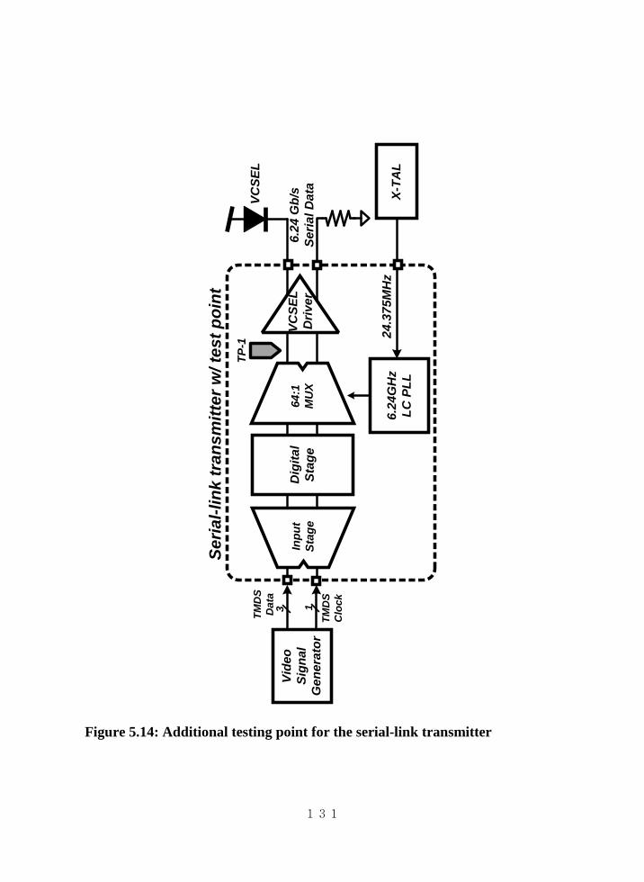
131
Vide
oSi
gnal
Gen
erat
or
3 1
TMD
S D
ata
TMD
S C
lock
VCSE
LD
river
VCSE
L
6.24
Gb/
sSe
rial D
ata
64:1
MU
X
6.24
GH
zLC
PLL
TP-1
X-TA
L
Seria
l-lin
k tr
ansm
itter
w/ t
est p
oint
24.3
75M
Hz
Inpu
tSt
age
Dig
ital
Stag
e
Figure 5.14: Additional testing point for the serial-link transmitter

132
Figure5.15: 6.24-Gb/s eye diagram at in front of VCSEL driver

133
Figure5.16: Photograph of the evaluation boards

134
(a)
(b)
Figure 5.17: Measurement setup for serial link: (a) block diagram and (b)
real photograph

135
(a)
(b)
Figure5.18: Simulated and measured DAV according to the video resolutions

136
Table 5.1 Simulated and measured DAV ratio according to the video
resolutions
TMDS rates
[Mb/s] TCLK20 DAV ratio
(Simulated) Average time @ DAV=1.8V (Measured)
Average time @ DAV=0V (Measured)
DAV ratio (Measured)
251.2 (VGA) 12.6 ~0.13 10.258ns 68.825ns ~0.13
400 (SVGA) 20 ~0.205 10.130ns 39.193ns ~0.205
650 (XGA) 32.5 ~0.33 10.213ns 20.485ns ~0.33
1080 (SXGA) 54 ~0.55 12.842ns 10.365ns ~0.55
1485 (1080p) 41.9 ~0.43 10.215ns 14.166ns ~0.43
1620 (UXGA) 81 ~0.83 50.043ns 10.165ns ~0.83

137
Figure5.19: TCLK20 according to the resolutions at DTEST of the receiver

138
Figure5.20: Recovered TMDS clock according to the resolutions at the output
of the receiver

139
Table 5.2 Performance summary
Parameters Serial-link transmitter Serial-link receiver
Tehcnology CMOS 0.18μm
Supply Voltage 3.3V single (Built-in regulator 3.3V to 1.8V)
Wavelength 850nm
Optical sensitivity - -19.4dBm for 1e-9 BER
-18dBm for 1e-12 BER
Total throughput 6.24Gb/s
Covered display resolutions VGA, SVGA, XGA, SXGA, UXGA, 1080p
Current Consumption
Total: 124mA input stage: 56mA
digital stage: 15mA output stage: 53mA
Total: 175mA input stage: 101mA digital stage: 15mA output stage: 59mA
Die size 1.75mm x 1.97mm 1.75mm x 2.08mm

140
5.2.4 Video transmission experiments
Through 700-m long MMF, real video transmission is verified as shown in
Figure 5.21. Video signal generator generates various videos from VGA to 1080p.
All of the videos in that ranges appropriately come true. For testing transmission
distance, Lightwave Measurement System (Agilent 8164A) is used as an optical
attenuator, as depicted in Figure 5.22. The output power of the VCSEL indicates -
4dBm, and the result shows the designed serial link can endure maximum 15-dB
attenuation. In other words, the optical sensitivity for the video transmission is -
19dBm. Used 62.5-μm normal MMF has 2.9dB/km of transmission loss.
Assuming 4-dB loss caused by connections between optical devices and MMF,
more than 5-km long of transmission distance is arithmetically possible. Since
almost display applications require below 500-m distance, the optical sensitivity is
sufficient to transmit the full-HD video, in spite of uncertainty for dispersions of
the MMF, such as material dispersion, waveguide dispersion, and modal
dispersion. In the experiments, the VCSEL-based serial link successfully transmits
full-HD video signals from display source to monitor up to 700-m long MMF.
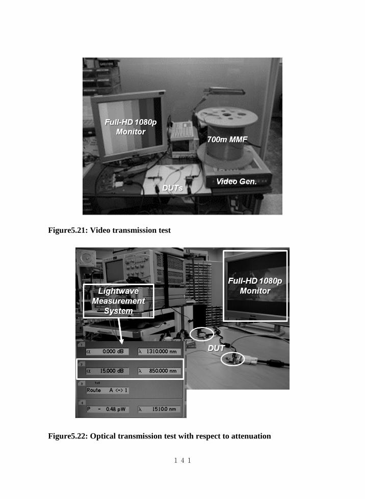
141
Figure5.21: Video transmission test
Figure5.22: Optical transmission test with respect to attenuation

142
CHAPTER 6
DISCUSSIONS AND CONCLUSIONS
6.1 Discussions on stationary-data-rate scheme
The stationary-data-rate scheme has some disadvantages compared with the
serial-link scheme having wide-range PLL and CDR. First is system overheads for
frequency-domain conversion. Figure 6.1 and 6.2 show the serial-link transmitter
and receiver architectures with and without wide-range PLL and CDR,
respectively. In the digital parts, an asynchronous FIFO, a DAV encoder, and a
DAV decoder are representative overheads. However additional costs of these
digital overheads, such as area and power, are not critical. Most critical overhead
is the use of a fractional PLL in the receiver side. To cover the various video
resolutions with only one fixed data rate, the fractional PLL accompanied with a
second-order DSM and complex digital filters is necessary. As analog overheads
like a multi-band VCO exist in the wide-range PLL and CDR, however, total
system complexity depends on its applications. Moreover, a frequency detector for
band selection of the multi-band VCO and additional digital blocks to avoid
harmonic-lock issue are needed for the continuous-rate CDR in the receiver side.
To extract the frequency directly from wide-range incoming data, frequency
detectors based on complicated FSM [20, 36-37] or run-length counter of 8B10B

143
coding [22] have been used. Figure 6.3 shows a block diagram of the continuous-
rate CDR using run-length counter. A digital frequency locked-loop including run-
length counter and divider controller was necessary in addition to a typical
narrow-band CDR.
Second is inefficient power consumption. The stationary scheme always
operates at the highest speed, while serial links using the wide-range serial link
can manage the dynamic power consumption according to the incoming data rate
by using a dynamic voltage scaling (DVS) and adaptive supply regulations [23].

144
60
clk2
0cl
k20
60
Hea
der
Gen
.
Scra
mble
r
60 4
Wid
e-Ran
ge
Oct
ave
PLL
800~
6240
Mb/s
Serial
ized
Dat
a
10~
87.5
MH
z
E/O
VCSE
L
Ran
ge
Det
.
Dat
aAlig
ner
2
Sim
ple
Dig
ital
Core
64:1
MU
X
250~
1950
Mb/s
TMD
S D
ATA
(x3
)
25~
195M
Hz
TMD
S Clo
ck
1:20
DEM
UX
with
C
DR
(x3)
Dat
aO
ut Clk
Out
250~
1950
Mb/s
TMD
S D
ATA
(x3
)
25~
195M
Hz
TMD
S Clo
ck
60
clk2
0
1:20
DEM
UX
with
C
DR
(x3)
Dat
aO
ut Clk
Out
Ran
ge
Det
.
Dat
aAlig
ner
FIFO
60
Dum
my
Enco
der
25x
12
DAV
Enco
der
1 0
60Sc
ram
ble
r60
64
4
Stat
ionar
y Sc
hem
eD
igital
Core
6.24
-GH
zLC
-PLL
X-t
al C
lock
24.4
1MH
z
E/O
VCSE
L
64:1
MU
X
6240
Mb/s
Serial
ized
Dat
a
3120
~ 6
240
MH
zW
ide-
Ran
ge
CD
R
Figure 6.1: Serial-link transmitter architecture with and without the wide-
range PLL and CDR

145
PIN
PD
6250
Mb/s
Serial
ized
Dat
a
O/E
1:64
DEM
UX
with
CD
R
X-t
al C
lock
24.4
1MH
z
64Bar
rel
Shifte
r
64
Shifte
rCnt.
5
De-
Scra
mble
r60
4D
AV
Dec
oder
FIFO
60
Ran
ge
Dec
oder
52
CLK
64 (
6.25
GH
z/64
)
60
∆-Σ
Fra
ctio
nal
PLL
250~
1950
Mb/s
TMD
S D
ATA
(x3
)
25~
195M
Hz
TMD
S Clo
ck
20:1
MU
X(x
3)
Stat
ionar
y Sc
hem
eD
igital
Core
800
~ 6
240
Mb/s
Continuous-
Rat
e CD
Rclk6
4
64D
e-sc
ram
ble
r60
1:64
DEM
UX
with
CR
-CD
R
60
3250~
1950
Mb/s
TMD
S D
ATA
(x3
)
25~
195M
Hz
TMD
S Clo
ck
PIN
PD
6240
Mb/s
Serial
ized
Dat
a
O/E
Rin
g P
LL
Bar
rel
Shifte
r
Sim
ple
Dig
ital
Core
Ran
ge
Dec
oder
420
:1M
UX
(x3)
Figure 6.2: Serial-link receiver architecture with and without the wide-range
PLL and CDR

146
Samplers(x4) CP-1
CP-2
8B10BEncoded
Data
LF VCO
ProgrammableDivider
%10
Digital Frequency Locked-Loop
(FPGA)
Run-lengthCounter
DividerController
1:10
DEM
UX
RotationalFrequencyDetector
BBPD
10
CLKVCO
Divider Control
Narrow RangeCDR
Parallel Data
Figure 6.3: Continuous-rate CDR architecture using 8B10B run-length
counter [22]
6.2 Future works
In a serial-link receiver, a sequence alignment is essential. Cascaded barrel
shifter is used for the sequence alignment as shown in Figure 6.4. As mentioned in
Chapter 4.3.1, cascaded barrel shifter exhibits 14 frame cycles (~140ns, 6 cycles
for shifting and 8 cycles for checking header bits) of latency in the worst case for
63-bit shifting. With matrix barrel shifter, we can reduce the latency to 9 frame
cycles (~90ns, 1 cycle for shifting and 8 cycles for checking) [38].
Future works for uncompressed display interconnects related with serial-link
transceivers are as follows. First, serial-link transceivers using wide-range PLL
and CDR will be researched for power-hungry applications like mobile-to-FPD

147
interconnects (micro HDMI). By using DVS, power-efficient serial-link
transceiver can be implemented. Second, the serial-link transceivers using
stationary-data-rate scheme will be upgraded for recent HDMI standards. In
recently released HDMI1.4a, TMDS data rate per channel is 3.4 Gb/s. Thus 10.88-
Gb/s serial-link transceiver is necessary for HDMI1.4a. HDMI1.4b standard for 3-
dimensional (3D) display interconnects are also released. To provide a full-HD 3D
display, HDMI1.4b has six data channels and one clock channel. To cover this
standard, 21.76-Gb/s serial-link transceiver should be researched. Third,
convergent interconnect systems combined with SERDES-based IC technology
and CWDM-based optical technology will be studied. Ultra high definition (UHD)
resolutions will be a standard of next-generation broadcasting. The 4K-UHD
(3840 by 2160) and 8K-UHD (7680 by 4320) requires fourfold and sixteen-times
bandwidth compared with the full-HD resolution. In short, 40-Gb/s ~ 160-Gb/s
data rate is necessary. This large bandwidth cannot be implemented using only IC
technology. Therefore both SERDES-based IC technology and CWDM-based
optical technology should be converged as shown in Figure 6.6.

148
SYNC
Stage 0Stage 5 Stage 4 Stage 3 Stage 2 Stage 1
SFT<
0>
Sync. monitor
SFT<
5>
SFT<
4>
SFT<
3>
SFT<
2>
SFT<
1>
Shift by(32,0)
Shift by(16,0)
Shift by(8,0)
Shift by(4,0)
Shift by(2,0)
Shift by(1,0)
IN<63:0> OUT<63:0>
Figure 6.4: Cascaded barrel shifter architecture
IN<63:0>
……
……
OU
T<63
:0>
Shift
C
ontr
ol
……
Figure 6.5: Matrix barrel shifter architecture

149
BO
SA4C
H x
20G
Opt
ical
A
FE
20G
b/s
SER
DES
(x4)
BO
SAB
OSA
BO
SA……
CW
DM
BO
SA4C
H x
20G
Opt
ical
A
FE
20G
b/s
SER
DES
(x4)
BO
SAB
OSA
BO
SA
……
CW
DM
Opt
ical
I/F
Elec
tric
al I/
F
IC T
echn
olog
yO
ptic
al T
echn
olog
y
- Up
Link
: λ1 ~
λ4
- Dow
n Li
nk: λ
5 ~ λ
8
80G
b/s
Bi-D
i Lin
kSy
stem
In
tegr
atio
nTe
chno
logy
Figure 6.6: Display interconnect systems combined with SERDES-based IC
technology and CWDM-based optical technology

150
6.3 Conclusions
As the consumer demands for HD videos have been increased, data capacity
of video technology becomes more and more. Therefore, the display interconnects
grow into one of the most critical parts of display systems more and more.
VCSEL-based 850-nm MMF link is one of the strongest solutions for the
uncompressed long-haul video transmissions.
HDMI display link consists of three data channels and one clock channel.
Therefore four optical device pairs and four MMFs are required. For lowering
system costs and improving system reliability, we realize single-fiber HDMI link
for long-haul display interconnects by using electrical SERDES. Unlike the other,
the serial link for display interconnects has to provide wide ranges depending on
incoming resolutions. We propose the stationary-data-rate architecture to cover
wide ranges without wide-range PLL and CDR. To realize stationary-data-rate
architecture, frequency-domain conversion between stationary clock and TMDS
clock is performed each other by FIFO, data valid signal, range codes, and
fractional PLL.
High-speed analog circuits including PLL, CDR, MUX, DEMUX, and
optical AFEs, and digital circuits are realized using 0.18-μm CMOS technology.
The implemented chipset is installed on PCB for prototype test. The functionality
and performance of the serial-link transmitter and receiver are verified with the

151
measurements. For testing purpose, built-in PRBS generator, PRBS error checker,
digital test bus, and analog test bus are embedded. In experiments, the VCSEL-
based serial link successfully transmits full-HD video signals from display source
to monitor up to 700-m long MMF.

152
REFERENCES
[1] J. Adam, Chi Shih Chang, J. J. Stankus, M. K. Iyer, W. T. Chen, “Addressing
packaging challenges,” IEEE Circuits and Devices Magazine, Vol. 18, Issue 4,
pp. 40-49, July 2002.
[2] B. S. Landman and R. L. Russo, “On a pin versus block relationship for
partitions of logic graphs,” IEEE Trans. On Comput., vol. C-20, pp. 1469-
1479, 1971.
[3] H. B. Bakoglu, Circuits, Interconnections, and Packaging for VLSI, Addison-
Wesley, 1990.
[4] E. G. Friedman et al., Clock Distribution Networks in VLSI Circuits and
Systems, IEEE Press, 1995.
[5] N. Maheshwari and S. S. Sapatnekar, Timing Analysis and Optimization of
Sequential Circuits, Kluwer, 1999.
[6] T. H. Lee, and J. F. Bulzacchelli, “A 155-MHz clock recovery delay- and
phase-locked loop, ” IEEE Journal of Solid-State Circuits, vol. 27, No. 12, pp.
1736 – 1746, Dec. 1992.
[7] B. Chia, R. Kollipara, D. Oh, C. Yuan and L. S. Boluna, “Study of PCB trace
crosstalk in backplane connector pin field,” IEEE Conference on Electrical
Performance of Electronic Packaging, pp. 281-284, Oct. 2006.

153
[8] E. Säckinger, “Broadband Circuits for Optical Fiber Communication,” Wiley,
2005.
[9] B. O’Donnell, “IDC White Paper, HDMITM
[10] NEC Display Solutions of America, Inc., “Video display interfaces,” NEC,
2008.
: The Digital Display Link,” IDC,
2006.
[11] HDMI Licensing, LLC., “High-Definition Multimedia Interface Specification
Version 1.4a,” March 4, 2010.
[12] Video Electronics Standard Association, “VESA and Industry Standards and
Guidelines for Computer Display Monitor Timing (DMT) Version 1.0,
Revision 12p, Draft 2,” VESA 2008.
[13] D. Boossert et al., “Production of high-speed oxide confined VCSEL arrays
for datacom applications,” Proc. SPIE, vol. 4649, pp. 142-151, June 2002.
[14] D. Vez et al., “10 Gbit/s VCSELs for datacom: devices and applications,”
Proc. SPIE, vol. 4942, pp. 29-43, Apr. 2003.
[15] J. Jewell et al., “1310nm VCSELs in 1-10Gb/s commercial applications,”
Proc. SPIE, vol. 6132, pp. 1-9, Feb. 2006.
[16] M. A. Wistey et al., “GaInNAsSb/GaAs vertical cavity surface emitting lasers
at 1534nm,” Electronics Letters, vol. 42, no. 5, pp. 282-283, Mar. 2006.

154
[17] H. S. Lee, S. S. Lee, and Y. S. Son, “CWDM based HDMI interconnect
incorporating passively aligned POF linked optical subassembly modules,”
Optics Express, vol. 19, issue 16, pp. 15380-15387, Aug. 2011.
[18] M. Teitelbaum and K. W. Goossen, “Reliability of Direct Mesa Flip-chip
Bonded VCSEL’s,” IEEE Lasers and Electro-Optics Society Annual Meeting,
Nov. 2004.
[19] M. Zhang, M. R. Haider, S. K. Islam, R. Vijayaraghavan, and A. B. Islam, “A
low-voltage low-power programmable fractional PLL in 0.18-um CMOS
process,” Analog Integrated Circuits and Signal Processing, vol. 65, no. 1, pp.
33-42, March 2010.
[20] R. –J. Yang, K. –H. Chao, S. –C. Hwu, C. –K. Liang, and S. –I. Liu, “A
155.52 Mbps – 3.125 Gbps Continuous-Rate Clock and Data Recovery
Circuit,” IEEE Journal of Solid-State Circuits, vol. 41, no. 6, pp. 1380-1390,
June 2006.
[21] Inhwa Jung, Daejung Shin, Taejin Kim, and Chulwoo Kim, “A 140 Mb/s to
1.96 Gb/s Referenceless Transceiver With 7.2us Frequency Acquisition
Time,” IEEE Trans. On VLSI Systems, vol. 19, no. 7, pp. 1310-1315, July
2011.
[22] M. S. Hwang, S. Y. Lee, J. K. Kim, S. H. Kim, and D. K. Jeong, “A 180-
Mb/s to 3.2-Gb/s, Continuous-Rate, Fast-Locking CDR without Using
External Reference Clock,” IEEE Asian Solid-State Circuits Conference, pp.
144-147, Nov. 2007.

155
[23] G. Balamurugan et al., “A Scalable 5-15Gbps, 14-75mW Low Power I/O
Transceiver in 65nm CMOS,” IEEE Journal of Solid-State Circuits, vol. 43,
no. 4, pp. 1010-1019, Apr. 2008.
[24] F. Tobajas et al., “A Low Power 2.5 Gbps 1:32 Deserializer in SiGe BiCMOS
Technology,” in IEEE Proc. Design and Diagnostics of Electronic Circuits
and Systems, Prague, Czech, July 2006, pp. 19-24.
[25] J. K. Kim, J. Kim, G. Kim, and D. K. Jeong, “A Fully Integrated 0.13-μm
CMOS 40-Gb/s Serial Link Transceiver,” IEEE Journal of Solid-State
Circuits, vol. 44, no. 5, pp. 1510-1521, May 2009.
[26] W. S. Oh and K. Park, “A 12.5-Gb/s Optical Transmitter using an Auto-
Power and –Modulation Control,” Journal of the Optical Society of Korea,
vol. 13, no. 4, pp. 434-438, Dec. 2009.
[27] HFD7192-xxx LC TOSA Package data sheet Rev. D, Advanced Optical
Components Division, Finisar Corporation, 2007.
[28] S. M. Park and H. J. Yoo, “1.25-Gb/s Regulated Cascode CMOS
Transimpedance Amplifier for Gigabit Ethernet Applications,” IEEE Journal
of Solid-State Circuits, vol. 39, no. 1, pp. 112-121, Jan. 2004.
[29] http://www.finisar.com/sites/default/files/pdf/8mZ2hQHFD7180%20Rev%20
C.pdf, accessed September 2012.
[30] K. Park, W. S. Oh, and W. Y. Choi, “A 10-Gb/s trans-impedance amplifier
with LC-ladder input configuration,” IEICE Electronics Express, vol. 7, no.
16, pp. 1201-1206, Dec. 2010.

156
[31] W. –Z. Chen and D. –S. Lin, “A 90-dBΩ 10-Gb/s Optical Receiver Analog
Front-End in a 0.18-μm CMOS Technology,” IEEE Trans. On VLSI Systems,
vol. 15, no. 3, pp. 358-365, March 2007.
[32] K. S. Yoo, D. M. Lee, G. H. Lee, S. M. Park, and W. S. Oh, “A 1.2V 5.2mW
40dB 2.5Gb/s limiting amplifier in 0.18-μm CMOS using negative
impedance compensation,” in IEEE International Solid-State Circuit
Conference, San Francisco, CA, USA, Feb. 2007, pp. 23-24.
[33] R. Inti et al., “A Highly Digital 0.5-to-4Gb/s 1.9mW/Gb/s Seril-Link
Transceiver Using Current-Recycling in 90nm CMOS,” in IEEE International
Solid-State Circuit Conference, San Francisco, CA, USA, Feb. 2011, pp. 152-
153.
[34] W. Yin et al., “A TDC-less 7mW 2.5Gb/s Digital CDR with Linear Loop
Dynamics and Offset-Free Data Recovery,” IEEE Journal of Solid-State
Circuits, vol. 46, no. 12, pp. 3163-3173, Dec. 2011.
[35] M. Assaad and R. S. Cumming, “20 Gb/s referenceless quarter-rate PLL-
based Clock Data Recovery Circuit in 130-nm CMOS Technology,” in Proc.
Int. Conf. on MIXDES, Poznan, Poland, June 2008, pp. 147-150.
[36] R. –J. Yang, K. –H. Chao, and S. –I. Liu, “A 200-Mbps ~ 2-Gbps
Continuous-Rate Clock-and-Data-Recovery Circuit,” IEEE Trans. On
Circuits and Systems I, vol. 53, no. 4, pp. 842-847, Apr. 2006.
[37] D. Dalton, K. Chai, E. Evans, M. Ferriss, D. Hitchcox, P. Murray, S.
Selvanayagam, P. Shepherd, and L. D. Vito, “A 12.5-Mb/s to 2.7-Gb/s
Continuous-Rate CDR With Automatic Frequency Acquisition and Data-Rate

157
Readback,” IEEE Journal of Solid-State Circuits, vol. 40, no. 12, pp. 2713-
2725, Dec. 2005.
[38] W. Yang, W. Schofield, H. Shibata, S. Korrapati, A. Shaikh, N. Abaskharoun,
and D. Ribner, “A 100mW 10MHz-BW CT ΔΣ Modulator with 87dB DR
and 91dBc IMD,” in IEEE International Solid-State Circuit Conference, San
Francisco, CA, USA, Feb. 2008, pp. 498-499.