Embed Size (px)
Citation preview

HIGH-VOLUME-MANUFACTURING (HVM) OF BVA ENABLED ADVANCED PACKAGE-ON- PACKAGE (POP)
Rajesh Katkar, Ashok S. Prabhu and Wael Zohni Invensas Corporation San Jose, CA, USA
ABSTRACT Bond Via Array (BVA) technology utilizes existing wirebond assembly infrastructure to enable high density vertical interconnects required for next generation electronics products. One area that can benefit from BVA is Package-on-Package (PoP) for memory/processor and other combinations used in mobile electronics applications. PoP provides board space savings by vertically stacking the memory atop the processor package. The close coupling between the stacked components also facilitates reduced power operation. Recent product design trends have furthermore set forth requirements for increased IO count between memory and processor in order to increase bandwidth while reducing operating frequency. BVA enables assembly capability for achieving more than 1000 vertical connections between the memory and processor components in an industry standard PoP outline. This figure more than doubles current PoP assembly capability thereby addressing next generation high IO mobile device demands for increased bandwidth [1]-[3]. In this paper, we will present validation data for BVA high volume manufacturing including optimization of assembly process, yield, test and reliability.
INTRODUCTION Bond Via Array utilizes wirebond-based processing to create free-standing vertical bond structures that form a fine pitch interconnect. This approach differs significantly from the solder sphere/BGA PoP stack construction used today. Current use of solder spheres in BGA PoP imposes a geometrical relationship between lateral pitch and height of the vertical interconnect; in order to reduce pitch, solder sphere diameter must be reduced which in turn reduces the overall height of the resulting solder column. In contrast, the BVA configuration allows vertical bond height to be specified independent of required pitch. In the case of SoC/memory PoP, this decoupling enables higher density interconnect that accommodates thickness requirements for the underlying SoC device (see Figure 1).
Figure 1: Cross-section showing BVA as fine pitch interconnect between Memory and SOC
Package-on-Package is the most popular way to assemble the processor and memory subunit in today’s mobile applications. Existing standard outline PoP solutions are able to provide only about 300-500 interconnects between the processor and the memory package. This arrangement limits memory data interconnects to 64 lines, for a corresponding bandwidth of up to 25.6 GB/s at 1600 MHz DDR signal speeds. With a trend towards System-on-Chip (SoC) mobile processors with multi-core CPU, memory bandwidth requirements are sharply increasing. Also as the processor die size increases the peripheral space on the processor package gets limited; one has to then consider growing the package size to meet the higher interconnect needs. To meet these emerging requirements, new memory standards such as wide-IO 2 have been proposed to provide up to 512 memory data interconnects. This standard provides almost 3 times current bandwidth (>65 GB/s) at lower 800 MHz DDR signal speeds. For memory devices to offer 512 data lines, about 1000 interconnects are required in order to include the accompanying address, control, power and ground signals required for operation.
Existing PoP solutions are not capable of offering >1000 interconnects as they cannot achieve the required pitch values of ≤0.24mm within the standard 14mm x 14mm package footprint. Free-standing solder sphere BGA stacking is limited to approximately 0.400mm pitch. Through-Mold-Via (TMV) stacking used today provides incremental improvement to BGA stacking by introducing laser-drilled cavities in mold that laterally contain solder sphere at finer pitches of about 0.350mm. This method still requires significant die thinning due to assembly process limitations. On the development front there is 3DIC or Through-Silicon-Via (TSV) technology for direct stack of devices. Although TSV is an ideal high-bandwidth solution the technique remains expensive and is not expected to be practical for the broad market over the next few years. Table 1 below shows a comparison between these existing interconnect technologies and BVA.
Proceedings of SMTA International, Sep. 27 - Oct. 1, 2015, Rosemont, IL Page 1
As originally published in the SMTA Proceedings.

Table 1: Comparison of TMV, BVA and TSV Technologies
A BVA test vehicle demonstrating 1020 PoP interconnects at 0.24mm pitch was assembled within the conventional 14mm x14mm outline package specification. This vehicle has been utilized to develop and verify assembly materials and process as well as for package reliability test and validation (Table 2 below):
Table 2: 1020IO TV Package Details
Package foot print 14mm x 14mm Package Thickness 1.25mm Logic Package Thickness 0.74mm Memory Package Thickness 0.51mm Logic BGA Pitch 0.4mm Number of Logic IOs 916 PoP IO Pitch 0.24mm Number of PoP IO rows 5 Number of PoP IOs 1020
As indicated in Table 2, there are a total of 5 rows of bond via interconnects at 240m pitch distributed about the periphery of a 150um thick 7.5mm x 7.5mm logic flip-chip die. These bond-vias provide a total of 1020 connections between the bottom logic and top memory package. The topside of the logic substrate correspondingly has flip-chip pads at the central region of the component while providing wire-bond pads at the periphery for planting of the vertical bonds. The terminal side of the topside memory component provides a solder pad arrangement matching the logic package’s peripheral bond via array. The following provides details on baseline BVA assembly process as well as improvements for volume manufacturing. In addition to verifying High-Volume-Manufacturing (HVM) readiness of BVA technology the 1020IO vehicle has been utilized to demonstrate improvements on key process steps such as bonding and molding. The core processes developed for BVA include free standing vertical BVA-bond formation, film assist molding and fine-pitch package-on-package stacking. Extension of the technology from the originally qualified 2.0mil to 1.5mil diameter copper wire is also being pursued. Finally manufacturing
validation activity of BVA at subcontract package assembly facilities is also provided. HVM READINESS OF BVA As mentioned, BVA leverages the fine-pitch bonding capability of wirebond equipment in order to achieve a vertical interconnect structure that is readily producible with today’s assembly infrastructure. Previous papers [4] have illustrated the details of this compatibility. To supplement the development engineering work completed in prototype lab, BVA technology has now been implemented at subcontractors in Asia using large scale format material and equipment set-ups. This HVM subcontract engineering qualification utilized the same 1020IO BVA component vehicle design converted to a large-format substrate strip layout. The HVM engineering qualification version vehicle was run on a production scale strip format. As shown on Table 3, whereas initial prototype assembly utilized a 100x74mm half-size strip format, the HVM validation at assembly subcontractors implemented full-size strips typically used in package production. Larger strip sizes facilitate more efficient use of assembly equipment and materials thus significantly decrease unit assembly cost. Demonstrating the fundamental BVA process developed during prototyping in a production environment has enabled process refinements that ensure high yield and throughput at this increased scale.
Table 3: Prototype and HVM Strip Outlines
The process flow used at these production subcontractors to assemble the Logic package is based on the baseline process described in Figure 2. As show in in Table 4, The specific flows utilized at the two HVM locations represent this original flow with the only variations being the type of mold process used; HVM Partner 2 used a compression mold with film assist, while HVM Partner 1 & Invensas used a transfer mold with film assist. This variation is indicative of the adaptability of the BVA assembly process to conventional assembly line equipment.
Proceedings of SMTA International, Sep. 27 - Oct. 1, 2015, Rosemont, IL Page 2

Flux dip/mount top (memory)
package
Figure 2: Baseline BVA Assembly Flow As shown, the BVA process is compatible with BGA packaging assembly equipment. The key process steps introduced by the BVA process are vertical wirebond, film-assisted molding, and plasma etch deflash. Moving from a half-size to full-size substrate strip format required some adjustment to equipment set up. Table 4: HVM Process Flow For Logic Package
Invensas HVM Partner 1 HVM Partner 2
Substrate bake Substrate bake Substrate bake
Ar/O2 Plasma Ar/O2 Plasma Ar/O2 Plasma
FC Attach, Reflow FC Attach, Reflow FC Attach, Reflow
Flux Clean, Bake‐out Flux Clean, Bake‐out Flux Clean, Bake‐out
Ar/02 Plasma Ar/02 Plasma Ar/02 Plasma
Underfill & Cure Underfill & Cure Underfill & Cure
Ar/O2 plasma Ar/O2 plasma Ar/O2 plasma
BVA Wirebond BVA Wirebond BVA Wirebond
Ar/O2 Plasma Ar/O2 Plasma Ar/O2 Plasma
Pre‐Mold Bake Pre‐Mold Bake Pre‐Mold Bake
Transfer Mold w/ Film
Assist
Transfer Mold w/ Film
Assist
Compression Mold w/
Film Assist
Post Mold Cure Post Mold Cure Post Mold Cure
CF4 Plasma CF4 Plasma CF4 Plasma
Singulation & Bake Out Singulation & Bake Out Singulation & Bake Out
Ball Attach & Reflow Ball Attach & Reflow Ball Attach & Reflow
Flux Clean & Bake‐out Flux Clean & Bake‐out Flux Clean & Bake‐out
Final Visual Inspection Final Visual Inspection Final Visual Inspection
ASSEM
BLY FLO
W
Vertical wirebonding was performed on the same K&S ICONN wirebond equipment platform as that used during prototyping. The larger format strip size only required minor reprogramming in order to accommodate the expanded array of units. BVA bonding assembly yield and throughput demonstrated at the production facilities was confirmed to be comparable to that of conventional point-to-point wirebonding used widely in high-volume production. Table 5 below shows BVA bonding yield information for engineering qualification lot builds at HVM locations.
Table 5: BVA Bond Yield Data For Qual Lot Build
As seen above the BVA process yielded better than 99.5% (BVA yield). Yield loss was primarily due to unrelated manual setup issues. Bond integrity tests like ball shear were also performed and met all required criteria. Bond strength as well as height and location accuracy were measured and confirmed to fall well within specifications. Table 6 below summarizes these results. The film assist molding process utilized Yamada mold for the Invensas built parts. As noted before one of the external HVM assembly sites used a film assisted transfer mold while the other used a film assisted compression mold. In a film assisted transfer mold the BVA tips first get embedded in the film and then the mold compound is injected into the cavity encapsulating the BVA whereas in the case of compression mold, the BVA travels through the molten mold compound layer and then gets embedded in the film. BVA processing was compatible with both of these approaches to the molding process.
Table 6: Ball Integrity and Dimension Statistics
Extensive plasma etch process optimization for mold deflash was performed in order to address the increased treatment area required for large strip sizes. These larger geometries resulted in modified tooling designs and parameters that ensured effective mold flash removal over the entire strip area. Furthermore, evaluations of various plasma gas combinations were initiated to determine alternatives that address potential cost and regulatory requirement needs that vary across locations of production facilities. For example, using CF4 plasma in some countries
Proceedings of SMTA International, Sep. 27 - Oct. 1, 2015, Rosemont, IL Page 3

(like Korea) poses more expense due to such regulatory requirements. In this case, Ar/O2 gas was evaluated as an alternative to CF4/O2. For the large strip evaluations, the FLEXTRAK system from March Nordson was used. Results of evaluations for plasma optimization are summarized in Table 7 below:
Table 7: Plasma Optimization Evaluation Results
CF4 O2 ArHigh Low NA NGLow High NA GoodNA Low High NGNA High Low Good
Plasma GasResult
As shown, increased levels of O2 helped in both CF4/O2 and Ar/O2 combination cases (see Figures 3 and 4). Closely related to the plasma process is the BVA bond tip formation. The shape of the BVA tip affects how effectively it penetrates into the barrier film layer for protection against residual deposit during mold. Thus the degree of mold flash remaining on BVA tips is a function of the BVA tip shape. Optimization of the BVA bond tip to minimize mold flash is described in the following section. This tip shape optimization contributed to dramatically reducing the degree of required plasma etch exposure.
Figure 3: BVA Tips after Ar/O2 Plasma Exposure
Figure 4: BVA Tips After CF4/O2 Plasma Exposure EDX surface analysis was performed at different locations along the wire tip post plasma etch to confirm that the Pd coating on the wire was not affected by the plasma treatment. Results of the EDX are show below in Figure 5.
Figure 5: EDX Results of BVA Post Plasma
Although Figure 5 indicates some exposed copper area at the shear face of the BVA bond, most of the BVA-tip retains an intact Pd-coated surface. Furthermore, post High Temperature Stress Test (HTS) has shown the copper dissolution is very limited (Figure 6). These results in addition to other environmental test exposure and analysis indicates the Pd provides an effective barrier layer against copper dissolution of the copper into the solder.
Proceedings of SMTA International, Sep. 27 - Oct. 1, 2015, Rosemont, IL Page 4

Figure 6: SEM: BVA Tip in Solder Post-1000HRS HTS BOND TIP OPTIMIZATION In order maximize mechanical robustness while minimizing mold flash on finished BVA bond tips, the bond process was modified to produce a more controlled wedge shape at the resulting tip. Earlier efforts at BVA tip formation had resulted in a flattened web style tip structure as displayed in Figure 7 below:
Figure 7: Early Stage Web-shaped Wire Tip
With a web-shaped tip the wire end is compressed and widened to span a distance that is greater than the original wire diameter itself. During film assisted molding, this webbed tip creates a larger penetration radius leading to compromised forming of the film about the exposed wire span. Consequently more mold flash accumulates on the tip. Using a negative face angle capillary, the BVA tip was optimized into a controlled wedge shape that remained within bounds of the wire diameter, as shown in Figure 8.
Figure 8: Improved Wedge-shape Tip BVA This formation allows the mold film to more readily adhere to the entire wire tip span thus significantly reducing the amount of mold flash (Figure 9).
Figure 9: Post-Mold Wedge-Tip with No Mold Flash Extensive test socket insertion cycling validation was performed with this improved tip to confirm mechanical robustness and reliability. A load of 30g per wire was applied during each insertion with no observable damage occurring (Figure 10).
Figure 10: BVA Tip Pre- and Post-Socket Insertion Furthermore, BVA planar location accuracy and height were measured and found to maintain specifications.
Figure 11: 2-mil BVA Tip Displacement
Proceedings of SMTA International, Sep. 27 - Oct. 1, 2015, Rosemont, IL Page 5

WIRE DIAMETER REDUCTION: 2.0 TO 1.5MIL BVA BVA was originally developed using 2.0mil diameter copper wire. Reducing wire diameter from 2.0mil to 1.5mil provides some advantages including:
a. Enabling finer pitch BVA b. Reducing need for bonder heavy clamp kit
An engineering evaluation build was completed at Invensas using 1.5mil diameter wire in order to evaluate process and reliability of the resulting structure. Trials showed that controlled tip bonding could readily be accomplished with this wire diameter. Furthermore, the mechanical robustness of the BVA tips remained sufficient for assembly, handling and socketing exposure. BVA location accuracy and dimensions also were maintained within specifications as shown below in Figure 12.
Figure 12: 1.5mil BVA Tip Displacement and Height Nominal BVA height used was 440um (+/- 20um). Extensive bond mechanical integrity tests were performed including tensile pull as well as ball shear. Results indicated strong bonding and are shown below.
Table 8: 1.5 MIL Wire Tensile and Ball Shear Test
Post mold (325um mold cap) the BVA interconnects were subjected to similar socket insertion testing as described before. No major damage was observed to the BVA tips as shown in Figure 13 below. Furthermore, stacking performed with conventional pick and place equipment demonstrated >99.9% assembly yield.
Figure 13: 1.5-mil BVA Tip Pre- and Post-Socket Test
RELIABILITY TESTING Similar to prototypes from early stage development, engineering assembly lots completed at HVM facilities were subjected to a complete set of reliability tests including JEDEC level 3 moisture sensitivity, board level temperature cycling, high temperature storage and drop testing. At this time the testing of HVM Partner 2 has been successfully completed and the results are summarized below in Table 9. Qualification of HVM Partner 1 is in progress.
Table 9: Reliability Test and Results of HVM Partner 2
Test Standard Test Condition
Sample Size
Result
Moisture Sensitivity Level 3
IPC/JEDEC J-STD-020C
125°C for 24hrs; 30°C / 60%RH for 192 hrs, 3X Pb-free reflow
22
Passed
Unbiased ACLV
JESD22-A102D Condition D
121C 100%RH 168hr
22 Passed
Temperature Cycling (Board Level)
JESD22-A104D Condition G
-40°C to 125°C, 1000 cycles
45 Passed
High Temperature Storage
JESD22-A103D Condition B
150°C, 1000 hrs
22
Passed
Drop Testing JESD22-B111
>30drops, 1500G, 0.5mS of 1/2 sine pulse
22 Passed
Reliability testing was also performed on 1.5mil wire BVA interconnected PoP stack test vehicle parts. The results are summarized in the Table 10 below.
Proceedings of SMTA International, Sep. 27 - Oct. 1, 2015, Rosemont, IL Page 6
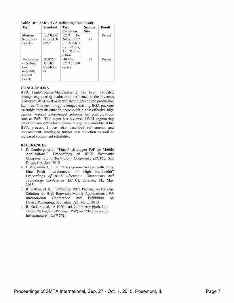
Table 10: 1.5MIL BVA Reliability Test Results Test Standard Test
Condition Sample Size
Result
Moisture Sensitivity Level 3
IPC/JEDEC J-STD-020C
125°C for 24hrs; 30°C / 60%RH for 192 hrs, 3X Pb-free reflow
25
Passed
Temperature Cycling (no underfill) (Board Level)
JESD22-A104D Condition G
-40°C to 125°C, 1000 cycles
25 Passed
CONCLUSIONS BVA High-Volume-Manufacturing has been validated through engineering evaluations performed at the Invensas prototype lab as well as established high-volume production facilities. This technology leverages existing BGA package assembly infrastructure to accomplish a cost-effective high density vertical interconnect solution for configurations such as PoP. This paper has reviewed HVM engineering data from subcontractors demonstrating the scalability of the BVA process. It has also described refinements and improvements lending to further cost reduction as well as increased component reliability.
REFERENCES 1. P. Damberg, et al, “Fine Pitch copper PoP for Mobile
Applications,” Proceedings of IEEE Electronic Components and Technology Conference (ECTC), San Diego, CA, June 2012
2. I Mohammed, et al, “Package-on-Package with Very Fine Pitch Interconnects for High Bandwidth” Proceedings of IEEE Electronic Components and Technology Conference (ECTC), Orlando, FL, May 2013
3. R. Katkar, et al, “Ultra-Fine Pitch Package on Package Solution for High Banwidth Mobile Applications”, 9th International Conference and Exhibition on Device Packaging, Scottsdale, AZ, March 2013
4. R. Katkar, et.al, “A 1020-lead, 240 micron pitch, 14 x 14mm Package-on-Package (PoP) and Manufacturing Infrastructure” ICEP 2014
Proceedings of SMTA International, Sep. 27 - Oct. 1, 2015, Rosemont, IL Page 7