Embed Size (px)
Citation preview

HIGH FIELD TRANSPORT PHENOMENAIN WIDE BANDGAP SEMICONDUCTORS
a thesis
submitted to the department of physics
and the institute of engineering and science
of bilkent university
in partial fulfillment of the requirements
for the degree of
master of science
By
Cem Sevik
September, 2003

I certify that I have read this thesis and that in my opinion it is fully adequate,
in scope and in quality, as a thesis for the degree of Master of Science.
Assist. Prof. Dr. Ceyhun Bulutay (Advisor)
I certify that I have read this thesis and that in my opinion it is fully adequate,
in scope and in quality, as a thesis for the degree of Master of Science.
Prof. Dr. Ekmel Ozbay
I certify that I have read this thesis and that in my opinion it is fully adequate,
in scope and in quality, as a thesis for the degree of Master of Science.
Assoc. Prof. Dr. Cengiz Besikci
Approved for the Institute of Engineering and Science:
Prof. Dr. Mehmet B. BarayDirector of the Institute Engineering and Science
ii

ABSTRACT
HIGH FIELD TRANSPORT PHENOMENA IN WIDEBANDGAP SEMICONDUCTORS
Cem Sevik
M.S. in Physics
Supervisor: Assist. Prof. Dr. Ceyhun Bulutay
September, 2003
The Ensemble Monte Carlo (EMC) method is widely used in the field of com-
putational electronics related to the simulation of the state of the art devices.
Using this technique our specific intention is to scrutinize the high-field transport
phenomena in wide bandgap semiconductors (Such as GaN, AlGaN and AlN).
For this purpose, we have developed an EMC-based computer code. After a brief
introduction to our methodology, we present detailed analysis of three different
types of devices, operating under high-field conditions, namely, unipolar n-type
structures, avalanche photodiodes (APD) and finally the Gunn diodes. As a test-
bed for understanding impact ionization and hot electron effects in sub-micron
sized GaN, AlN and their ternary alloys, an n+−n−n+ channel device is employed
having a 0.1 µm-thick n region. The time evolution of the electron density along
the device is seen to display oscillations in the unintentionally doped n-region, un-
til steady state is established. The fermionic degeneracy effects are observed to be
operational especially at high fields within the anode n+-region. For AlxGa1−xN-
based systems, it can be noted that due to alloy scattering, carriers cannot acquire
the velocities attained by the GaN and AlN counterparts. Next, multiplication
and temporal response characteristics under a picosecond pulsed optical illumi-
nation of p+-n-n+ GaN and n-type Schottky Al0.4Ga0.6N APDs are analyzed. For
the GaN APD, our simulations can reasonably reproduce the available measured
data without any fitting parameters. In the case of AlGaN, the choice of a Schot-
tky contact APD is seen to improve drastically the field confinement resulting in
satisfactory gain characteristics. Moreover, alloy scattering is seen to further slow
down the temporal response while displacing the gain threshold to higher fields.
Finally, the dynamics of large-amplitude Gunn domain oscillations from 120 GHz
to 650 GHz are studied in detail by means of extensive EMC simulations. The
basic operation is checked under both impressed single-tone sinusoidal bias and
external tank circuit conditions. The width of the doping-notch is observed to
iii

iv
enhance higher harmonic efficiency at the expense of the fundamental frequency
up to a critical value, beyond which sustained Gunn oscillations are ceased. The
degeneracy effects due to the Pauli Exclusion principle and the impact ionization
are also considered but observed to have negligible effect within the realistic op-
erational bounds. Finally, the effects of lattice temperature, channel doping and
DC bias on the RF conversion efficiency are investigated.
Keywords: High field transport, Ensemble Monte Carlo technique, Avalanche
photodiodes, Gunn diodes, Unipolar devices.

OZET
GENIS BANT ARALIKLI YARIILETKENLERDE
YUKSEK ELEKTRIK ALANI ALTINDA ILETIMOLAYLARI
Cem Sevik
Fizik, Yuksek Lisans
Tez Yoneticsi: Yard. Doc. Dr. Ceyhun Bulutay
Eylul, 2003
Toplu Monte Carlo (TMC) yontemi en modern aygıtların benzetimi maksadıyla,
genis bant aralıklı yarı iletkenlerde yuksek elektrik alanı altında iletkenligi in-
celemek icin kullanılmaktadır. Bizim amacımız, bu yontemi kullanarak genis
bant aralıklı yarı iletkenlerde (GaN, AlGaN and AlN gibi) yuksek elektrik alanı
altında iletkenligi genis bir sekilde incelemektir. Bu amaca uygun olarak, ilk
once TMC-tabanlı bir bilgisayar yazılımı gelistirilmistir. Yaklasımımız hakkında
kısa bir giristen sonra yuksek elektrik alanı altında calısabilen uc farklı aygıt
incelenmistir; tek kutuplu n-tipi yapı, cıg fotoalgılayıcıları ve Gunn diyot-
ları. Darbe iyonizasyonu ve ilgili sıcak-elektron etkilerini incelemek icin 0.1 µm
genisliginde n-katkılı bolge iceren (n+ − n − n+) yapısı kullanılmıstır. n-katkılı
bolge icerisinde elektron yogunlugunun duragan-hale ulasıncaya kadar zamana
gore salınım yaptıgı gorulmustur. Ayrıca yuksek elektrik alanı altında fermiy-
onik cakısıklık etkilerinin ozellikle n+-katkılı bolgede baskın oldugu gozlenmistir.
AlGaN yapısında elektronların hızının GaN ve AlN yapılarındaki elektronların
hızlarının arasında bir degerde olmadıgı ve bunun sebebinin de baskın alasım
sacınımının oldugu saptanmıstır. Daha sonra, GaN ve n-tipi Schottky Al-
GaN cıg fotoalgılayıcılarının carpma ve pico-saniyelik aydınlatma altında zamana
gore tepki karakteristigi analiz edilmistir. GaN foto algılayıcıları konusunda,
bizim benzetimlerimiz, hic bir oturtma parametresine gerek kalmadan mevcut
deneysel sonuclarla makul bir uyum gostermektedir. AlGaN yapısında, yuksek
kazanc saglayan bolgedeki elektrik alanını yukseltmek icin Schottky baglantılı
cıg fotoalgılayıcısı yapısının kullanılmasının uygun oldugu tesbit edilmistir. Ote
yandan, AlGaN yapısında, alasım sacınımının, aygıtın zamana gore tepkisini
yavaslatıgı ve kazanc esigini yuksek gerilimlere tasıdıgı gozlenmistir. Son olarak,
120 GHz´ten 650 GHz´e kadar genis-genlikli Gunn salınımları TMC yontemi ile
v

vi
detaylı bir sekilde incelenmistir. Gunn diyotların ozellikleri hem zorunlu uygu-
lanan tek-tonlu sinus gerilimi altında hem de dıs rezonans devresine baglanarak
kontrol edilmistir. Katkılama centiginin genisliginin yuksek harmoniklerdeki ver-
imi, belirli bir kritik degere kadar olumlu etkiledigi gozlenmistir. Pauli dısarlama
etkisinden kaynaklanan cakısıklık etkilerinin ve darbe iyonizasyonunun Gunn diy-
otun calısmasında cok etkili olmadıgı gorulmustur. En son olarak, orgu sıcaklıgı,
kanal katkılaması ve DC beslemesinin, RF donusturme verimi uzerindeki etkisi
incelenmistir.
Anahtar sozcukler : Yuksek elektrik alanı altında iletim, Toplu Monte Carlo
yontemi, Cıg fotoalgılayıcı, Gunn diyot, Tekkutuplu aygıtlar.

Acknowledgement
I would like to express my gratitude to my supervisor Assist. Prof. Dr. Ceyhun
Bulutay for his instructive comments in the supervision of the thesis.
vii

Contents
1 Introduction 1
1.1 This work . . . . . . . . . . . . . . . . . . . . . . . . . . . . . . . 2
2 Monte Carlo charge transport simulation 4
2.1 A typical MC program . . . . . . . . . . . . . . . . . . . . . . . . 4
2.1.1 Definition of the physical system and simulation parameters 6
2.1.2 Initialization . . . . . . . . . . . . . . . . . . . . . . . . . . 7
2.1.3 Free flight . . . . . . . . . . . . . . . . . . . . . . . . . . . 7
2.1.4 Identification of the scattering event . . . . . . . . . . . . 10
2.1.5 Choice of state after scattering . . . . . . . . . . . . . . . 12
2.2 MC simulation and the Boltzman Transport Equation . . . . . . . 14
2.3 The evolution of the Bilkent EMC code . . . . . . . . . . . . . . . 15
3 Hot electron effects in n-type structures 17
3.1 Computational details . . . . . . . . . . . . . . . . . . . . . . . . 18
3.2 Alloy scattering . . . . . . . . . . . . . . . . . . . . . . . . . . . . 19
viii

CONTENTS ix
3.3 Results . . . . . . . . . . . . . . . . . . . . . . . . . . . . . . . . . 20
4 AlGaN solar-blind avalanche photodiodes 23
4.1 Computational details . . . . . . . . . . . . . . . . . . . . . . . . 24
4.2 Results . . . . . . . . . . . . . . . . . . . . . . . . . . . . . . . . . 26
4.2.1 GaN APDs . . . . . . . . . . . . . . . . . . . . . . . . . . 26
4.2.2 Schottky contact-AlGaN APDs . . . . . . . . . . . . . . . 28
5 Gunn oscillations in GaN channels 32
5.1 Basics . . . . . . . . . . . . . . . . . . . . . . . . . . . . . . . . . 33
5.2 Motivation . . . . . . . . . . . . . . . . . . . . . . . . . . . . . . . 35
5.3 Computational details . . . . . . . . . . . . . . . . . . . . . . . . 36
5.4 Results . . . . . . . . . . . . . . . . . . . . . . . . . . . . . . . . . 37
5.4.1 The effect of notch width . . . . . . . . . . . . . . . . . . . 38
5.4.2 The effect of lattice temperature . . . . . . . . . . . . . . . 40
5.4.3 The effect of channel doping . . . . . . . . . . . . . . . . . 41
5.4.4 The effect of DC operating point . . . . . . . . . . . . . . 42
5.4.5 Connecting to a tank circuit . . . . . . . . . . . . . . . . . 43
5.5 Computational budget . . . . . . . . . . . . . . . . . . . . . . . . 44
6 Summary of the main findings 45
A Impact ionization and alloy scattering 52

CONTENTS x
A.1 Impact ionization . . . . . . . . . . . . . . . . . . . . . . . . . . . 52
A.2 Alloy scattering . . . . . . . . . . . . . . . . . . . . . . . . . . . . 56

List of Figures
2.1 Flowchart of the typical MC Program. . . . . . . . . . . . . . . . 5
2.2 (a)The path of the particle in wave-vector space. (b) The path of
the particle in real space. . . . . . . . . . . . . . . . . . . . . . . . 6
2.3 Total scattering rate versus energy for electrons in a model semi-
conductor. . . . . . . . . . . . . . . . . . . . . . . . . . . . . . . . 9
2.4 Fractional contribution versus energy for five scattering processes.
(1) Acoustic Deformation Potential, (2) Intervalley absorption, (3)
Intervalley emission, (4) Ionized impurity, (5) self scattering. . . . 10
2.5 Illustration of the procedure for identifying a scattering event. . . 11
2.6 (a) Scattering event in the (x, y, z) coordinate system. The incident
momentum is k and the scattered momentum, k′
. (b) The same
scattering event in the rotated coordinate system, (xr, yr, zr) by an
angle of φ about the x − axis, then θ about the the y − axis. In
the rotated system the incident momentum is kr and the scattered
momentum k′
r. . . . . . . . . . . . . . . . . . . . . . . . . . . . . 13
2.7 The empirical pseudopotential band structure of the GaN and AlN. 15
3.1 Structural schematic . . . . . . . . . . . . . . . . . . . . . . . . . 18
xi
LIST OF FIGURES xii
3.2 Velocity distribution over the n+−n−n+ channel under an applied
bias of 20 V. . . . . . . . . . . . . . . . . . . . . . . . . . . . . . . 19
3.3 Electric field distribution over the n+ − n − n+ GaN channel at
applied biases ranging from 5 V to 50 V. . . . . . . . . . . . . . . 20
3.4 Time evolution of the transient electron density profile over the
n+ − n − n+ GaN channel under an applied bias of 50 V; steady
state result is also shown, evaluated at 7.5 ps. . . . . . . . . . . . 21
3.5 (a) Steady state density profile at a bias of 50 V, with and without
the degeneracy effects included. (b) Energy distribution over the
n+ −n−n+ GaN channel under an applied bias of 80 V, with and
without impact ionization being included. . . . . . . . . . . . . . 22
4.1 Structural details. . . . . . . . . . . . . . . . . . . . . . . . . . . . 25
4.2 (a) Current gain of the GaN APD; EMC simulation (symbols)
compared with measurements [23] (dotted). (b) Current gain of
the Al0.4Ga0.6N APD simulated using EMC with and without alloy
scattering. Full lines in EMC curves are used to guide the eye. . . 26
4.3 Temporal response of the GaN and Al0.4Ga0.6N (vertically shifted
for clarity) APD to a 25 ps optical pulse, applied between the
dashed lines. . . . . . . . . . . . . . . . . . . . . . . . . . . . . . 28
4.4 Electric field distribution over (a) GaN (b) Al0.4Ga0.6N APDs at
several bias levels. . . . . . . . . . . . . . . . . . . . . . . . . . . . 29
4.5 Average velocity distribution over (a) GaN (b) Al0.4Ga0.6N APDs
for electron (solid) and holes (dotted). . . . . . . . . . . . . . . . 30
5.1 EMC simulation of the drift velocity versus field for bulk GaN at
300 K. . . . . . . . . . . . . . . . . . . . . . . . . . . . . . . . . . 33
5.2 Equivalent circuit for a uniform piece of semiconductor. . . . . . . 34

LIST OF FIGURES xiii
5.3 Structural details. . . . . . . . . . . . . . . . . . . . . . . . . . . . 36
5.4 (a) Typical charge density profiles for a 250 nm-notch device oper-
ating at the fundamental, second, third, fourth-harmonic modes,
each respectively vertically up-shifted for clarity. (b) Time evo-
lution of the electric field profile within one period of the Gunn
oscillation at 2 ps intervals for the 250 nm-notch device. . . . . . 38
5.5 Gunn diode efficiency versus frequency. (a) Effect of different
doping-notch widths, while keeping the total active channel length
fixed at 1.2 µm. (b) Effect of including the Pauli exclusion princi-
ple for the 250 nm-notch device. . . . . . . . . . . . . . . . . . . . 39
5.6 RF conversion efficiency versus frequency for several lattice tem-
peratures; 250 nm-notch device at 60 V bias is used. . . . . . . . . 40
5.7 RF conversion efficiency versus frequency for several channel dop-
ings; 250 nm-notch device at 60 V bias is used. . . . . . . . . . . . 41
5.8 RF conversion efficiency versus frequency for several DC bias volt-
ages; 250 nm-notch device. . . . . . . . . . . . . . . . . . . . . . . 42
5.9 Current and voltage waveforms for a 150 nm-notch Gunn diode (a)
under an imposed single-tone sinusoidal voltage, and (b) connected
to an external tank circuit shown in the inset. . . . . . . . . . . . 43
A.1 Electron II coefficient versus inverse electric field. Dotted lines
indicate the results when alloy scattering is not included, after
Jung [49]. . . . . . . . . . . . . . . . . . . . . . . . . . . . . . . . 55
A.2 Electron II coefficient versus inverse electric field. Dotted lines in-
dicate the results when alloy scattering is not included. The curves
for Al0.6Ga0.4N and Al0.8Ga0.2N merge at higher fields. These re-
sults are obtained for a temperature of 300 K and an ionized im-
purity concentration of 1017 cm−3. . . . . . . . . . . . . . . . . . 56

LIST OF FIGURES xiv
A.3 Electron energy distribution for Al0.4Ga0.6N at an electric field of
3.5 MV/cm, with (solid) and without (dotted) the alloy scattering.
A temperature of 300 K and an ionized impurity concentration of
1017 cm−3 are considered . . . . . . . . . . . . . . . . . . . . . . 57

List of Tables
4.1 Fitted temporal response functions exp(−t2/τ 2f ) and 1 −
exp(−t2/τ 2r ) cos(ωrt) for the GaN APD. . . . . . . . . . . . . . . . 27
4.2 Fitted temporal response functions exp(−t/τf ) and 1−exp(−t2/τ 2r )
for Al0.4Ga0.6N APD under a reverse bias of 30 V. . . . . . . . . . 30
A.1 Band edge analysis throughout the lowest two conduction bands of
AlxGa1−xN alloys: band edge energy, E, density of states effective
mass, m∗, and non-parabolicity factor, α (other than the lowest
valley, two-band ~k · ~p values are preferred). Equivalent valley mul-
tiplicities, Nv are included as well. Note that the ordering of the
U and K valleys is interchanged at an aluminium mole fraction of
0.6. . . . . . . . . . . . . . . . . . . . . . . . . . . . . . . . . . . . 53
A.2 A and K values in the electron II coefficient expression, A
exp(−K/F ), where, F is the electric field. A temperature of 300
K and an ionized impurity concentration of 1017 cm−3 are used. . 54
xv

Chapter 1
Introduction
The wide band gap semiconductors, especially GaN, AlN and their ternary al-
loys, are of increasing importance in various applications from high frequency,
high power amplifiers to blue and ultraviolet light emitters and detectors [1, 2].
Though these materials have much practical importance, they are still techno-
logically immature. As a result, their high-field transport properties and hence
the corresponding device potential are yet to be uncovered. Progress in assessing
the device potential of the wide band gap semiconductor materials is impeded
experimentally by the lack of sufficient device quality material which makes com-
putational approaches quite valuable in this respect.
The high-field transport, on the other hand, is in general a tough problem
[3], from both the mathematical and the physical points of view. In fact, the
integro-differential equation, the Boltzmann transport equation, that describes
the problem does not offer simple (or even complicated) analytical solutions ex-
cept for very few cases, and these cases usually are not applicable to real systems.
Furthermore, since transport quantities are derived from the averages over many
physical processes whose relative importance is not known a priori, the formula-
tion of reliable microscopic models for the physical system under investigation is
difficult. When one moves from linear to nonlinear response conditions, the diffi-
culties become even greater: the analytical solution of the Boltzmann transport
equation without linearization with respect to the external force is a formidable
1

CHAPTER 1. INTRODUCTION 2
mathematical problem, which has resisted many attacks in the last few decades.
In order to get any result, it is necessary to perform such drastic approximations
that it is no longer clear whether the features of interest in the results are due to
the microscopic model or to mathematical approximations.
From the foregoing it is understandable that, when two new numerical ap-
proaches to this problem, i.e., the Monte Carlo technique (Kurosawa, 1966) and
the iterative technique (Budd, 1966), were presented at the Kyoto Semiconduc-
tor Conference in 1966, hot-electron physicists received the new proposals with
great enthusiasm. It was in fact clear that, with the aid of modern large and fast
computers, it would become possible to obtain exact numerical solutions of the
Boltzmann equation for microscopic physical models of considerable complexity.
These two techniques were soon developed to a high degree of refinement by Price
(1968), Rees (1969), and Fawcett et al. (1970), and since then they have been
widely used to obtain results for various situations in practically all materials of
interest. The Monte Carlo method is by far the more popular of the two tech-
niques mentioned above, because it is easier to use and more directly interpretable
from the physical point of view.
The particular advantage of the Monte Carlo method is that it provides a
first principles transport formulation based on the exact solution of the Boltz-
mann equation, limited only by the extent to which the underlying physics of the
system is included. With these virtues, the ensemble Monte Carlo technique has
become our workhorse to tackle challenging high-field transport phenomena in
wide bandgap semiconductors, which are itemized in the following section.
1.1 This work
As a preliminary step in Chapter 3, we start with the high-field transport in
sub-micron sized, n-doped unipolar structures. Our analysis includes the alloy
scattering, impact ionization and degeneracy effects as well as the detailed tran-
sient time evolution of the electron density along the device. This part of the

CHAPTER 1. INTRODUCTION 3
thesis work has been published in the IEE Proceedings: Optoelectronics [4].
Next in Chapter 4, gain and temporal response characteristics of the GaN
and Al0.4Ga0.6N APDs are investigated. Especially the latter has technological
importance for the solar-blind photodetection. Results for the Al0.4Ga0.6N APDs
are provided both with and without the alloy scattering. To the best of our
knowledge, these simulations published in Applied Physics Letters [5] constitute
the only available data in the literature for this device.
Finally in Chapter 5, GaN-based Gunn diodes which can be utilized as a solid-
state high power millimeter wave oscillator are analyzed in detail. Particularly, we
show that the doping-notch width can be adjusted to enhance more efficient RF
conversion at higher harmonics than the fundamental frequency. The degeneracy
and impact ionization effects are observed to be insignificant. The effects of
channel doping, lattice temperature and the DC bias level are thoroughly studied.
A part of this chapter has been presented in 13th International Conference on
Non-equilibrium Carrier Dynamics in Semiconductors (Modena/Italy) and will
be published in the journal, Semiconductor Science and Technology [8].

Chapter 2
Monte Carlo charge transport
simulation
Much of our understanding of high-field transport in bulk semiconductors and
in devices has been obtained through Monte Carlo (MC) simulation, so it is
important to understand the basics of the method. Because it directly mimics
the physics, an understanding of the technique is also useful for the insight it
affords. One can find excellent resources on the MC technique [3, 6, 7, 10]; here,
we only include a brief introduction for documentation purposes which can be
skipped by those who feel familiar with the subject. Some details about the
Bilkent EMC code is also provided at the end of this chapter.
2.1 A typical MC program
For the sake of simplicity we shall refer to the case of electrons in a simple
semiconductor subject to an external electric field E1. The simulation starts with
electrons in given initial conditions with wave vector k0; then, the duration of
the first free flight is chosen with a probability distribution determined by the
scattering probabilities. During the free flight the external forces are made to act
1The contents of this section are not original and has been adopted from Lundstrom [6].
4
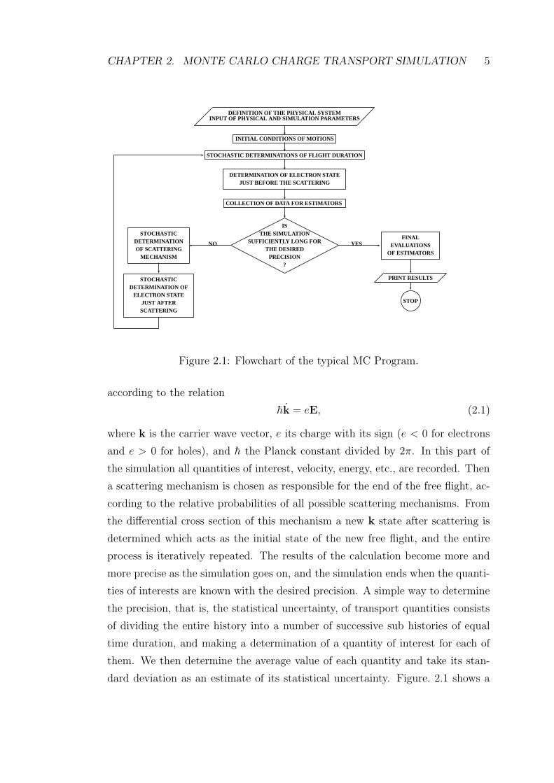
CHAPTER 2. MONTE CARLO CHARGE TRANSPORT SIMULATION 5
DEFINITION OF THE PHYSICAL SYSTEMINPUT OF PHYSICAL AND SIMULATION PARAMETERS
INITIAL CONDITIONS OF MOTIONS
STOCHASTIC DETERMINATIONS OF FLIGHT DURATION
DETERMINATION OF ELECTRON STATEJUST BEFORE THE SCATTERING
COLLECTION OF DATA FOR ESTIMATORS
ISTHE SIMULATION
SUFFICIENTLY LONG FORTHE DESIRED
PRECISION?
FINALEVALUATIONS
OF ESTIMATORS
STOCHASTICDETERMINATIONOF SCATTERING
MECHANISM
STOCHASTICDETERMINATION OF
ELECTRON STATEJUST AFTERSCATTERING
PRINT RESULTS
STOP
YESNO
Figure 2.1: Flowchart of the typical MC Program.
according to the relation
hk = eE, (2.1)
where k is the carrier wave vector, e its charge with its sign (e < 0 for electrons
and e > 0 for holes), and h the Planck constant divided by 2π. In this part of
the simulation all quantities of interest, velocity, energy, etc., are recorded. Then
a scattering mechanism is chosen as responsible for the end of the free flight, ac-
cording to the relative probabilities of all possible scattering mechanisms. From
the differential cross section of this mechanism a new k state after scattering is
determined which acts as the initial state of the new free flight, and the entire
process is iteratively repeated. The results of the calculation become more and
more precise as the simulation goes on, and the simulation ends when the quanti-
ties of interests are known with the desired precision. A simple way to determine
the precision, that is, the statistical uncertainty, of transport quantities consists
of dividing the entire history into a number of successive sub histories of equal
time duration, and making a determination of a quantity of interest for each of
them. We then determine the average value of each quantity and take its stan-
dard deviation as an estimate of its statistical uncertainty. Figure. 2.1 shows a

CHAPTER 2. MONTE CARLO CHARGE TRANSPORT SIMULATION 6
ky
kx
Momentum Spacey
x
Real Space
(a) (b)
Figure 2.2: (a)The path of the particle in wave-vector space. (b) The path of theparticle in real space.
flowchart of a simple MC program suited for the simulation of a stationary, ho-
mogeneous transport process. Figure. 2.2 illustrates the principles of the method
by showing the simulation in momentum k space and real space.
2.1.1 Definition of the physical system and simulation pa-
rameters
The starting point of the program is the definition of the physical system of inter-
est, including the parameters of the material and the values of physical quantities,
such as lattice temperature T0 and electric field. It is worth noting that, among
the parameters that characterize the material, the least known, usually taken as
adjustable parameters, are the coupling strengths describing the interactions of
the electron with the lattice and/or extrinsic defects inside the crystal. At this
level we also define the parameters that control the simulation, such as the dura-
tion of each sub history, the desired precision of the results, and so on. The next
step in the program is tabulation of each scattering rate as a function of elec-
tron energy. This step will provide information on the maximum value of these
functions, which will be useful for optimizing the efficiency of the simulation.

CHAPTER 2. MONTE CARLO CHARGE TRANSPORT SIMULATION 7
2.1.2 Initialization
Finally, all cumulative quantities must be put at zero in this preliminary part
of the program. In the particular case of a very high electric field, if an energy
of the order of kBT0 (kB being the Boltzmann constant) is initially given to the
electron, this energy will be much lower than the average energy in steady-state
conditions, and during the transient it will increase towards its steady-state value.
The longer the simulation time, the less influence the initial conditions will
have on the average results; however, in order to avoid the undesirable effects of
an inappropriate initial choice and to obtain a better convergence, the elimination
of the first part of the simulation from the statistics may be advantageous. The
simulation start with charge density which cancel the background impurity dop-
ing.
2.1.3 Free flight
After moving for a time, t, under the influence of a x-directed electric field, the
electron’s momentum and position are obtained from Eqs. 2.1.
r(t) = r(0) +∫ t
0υ(t
′
)dt′
. (2.2)
We assume that the field, Ex, is nearly constant for the duration of the free flight.
The first question to consider is: how long should the free flight continue - or what
is the time of the next collision? The duration of the free flight is directly related
to the scattering rate - the higher the scattering rate the shorter the average free
flight.
Within our approximations, we may simulate the actual transport by intro-
ducing a probability density P (t), where P (t)dt is the joint probability that a
carrier will both arrive at time t without scattering (after its last scattering event
at t = 0), and then will actually suffer a scattering event at this time (i.e., within
a time interval dt centered at t). The probability of actually scattering within this
small time interval at time t may be written as Γ[k(t)]dt, where Γ[k(t)] is the total
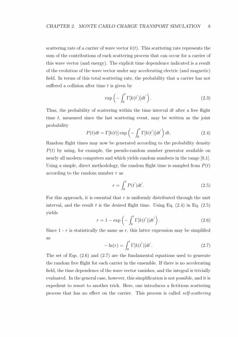
CHAPTER 2. MONTE CARLO CHARGE TRANSPORT SIMULATION 8
scattering rate of a carrier of wave vector k(t). This scattering rate represents the
sum of the contributions of each scattering process that can occur for a carrier of
this wave vector (and energy). The explicit time dependence indicated is a result
of the evolution of the wave vector under any accelerating electric (and magnetic)
field. In terms of this total scattering rate, the probability that a carrier has not
suffered a collision after time t is given by
exp(
−∫ t
0Γ[k(t
′
)]dt′
)
. (2.3)
Thus, the probability of scattering within the time interval dt after a free flight
time t, measured since the last scattering event, may be written as the joint
probability
P (t)dt = Γ[k(t)] exp(
−∫ t
0Γ[k(t
′
)]dt′
)
dt, (2.4)
Random flight times may now be generated according to the probability density
P (t) by using, for example, the pseudo-random number generator available on
nearly all modern computers and which yields random numbers in the range [0,1].
Using a simple, direct methodology, the random flight time is sampled from P (t)
according to the random number r as
r =∫ t
0P (t
′
)dt′
. (2.5)
For this approach, it is essential that r is uniformly distributed through the unit
interval, and the result t is the desired flight time. Using Eq. (2.4) in Eq. (2.5)
yields
r = 1 − exp(
−∫ t
0Γ[k(t
′
)]dt′
)
. (2.6)
Since 1 - r is statistically the same as r, this latter expression may be simplified
as
− ln(r) =∫ t
0Γ[k(t
′
)]dt′
. (2.7)
The set of Eqs. (2.6) and (2.7) are the fundamental equations used to generate
the random free flight for each carrier in the ensemble. If there is no accelerating
field, the time dependence of the wave vector vanishes, and the integral is trivially
evaluated. In the general case, however, this simplification is not possible, and it is
expedient to resort to another trick. Here, one introduces a fictitious scattering
process that has no effect on the carrier. This process is called self-scattering

CHAPTER 2. MONTE CARLO CHARGE TRANSPORT SIMULATION 9
1012
1013
1014
0 0.05 0.10 0.15 0.20 0.25 0.30
Scat
teri
ngra
te,Γ
(1/s)
Electron energy, (eV )
Γ0
ΓSELF = Γ0 − Γ(p)
Γ(p)
Figure 2.3: Total scattering rate versus energy for electrons in a model semicon-ductor.
(Fig. 2.3), and the energy and momentum of the carrier are unchanged under
this process (Rees, 1969). However, we will assign an energy dependence to this
process in just such a manner that the total scattering rate is a constant, as
Γself [k(t)] = Γ0 − Γ[k(t)] = Γ0 −∑
i
Γi[k(t)], (2.8)
and the summation runs over all real scattering processes. Its introduction eases
the evaluation of the free flight times, as now
tc = −1
Γ0
ln(r). (2.9)
With the addition of self-scattering, the total scattering rate is constant, so
Eq. (2.9) now applies, but we must be certain that the fictitious scattering mech-
anism introduced does not alter the problem. Real scattering events alter the
carrier’s momentum, but when a self-scattering event occurs we do not change
the carrier’s momentum. Self-scattering does not affect the carrier’s trajectory -
it simply makes the scattering rate constant so that Eq. (2.9) applies. When a
free flight is terminated by a fictitious scattering event, a new random number is
generated and the free flight continues.

CHAPTER 2. MONTE CARLO CHARGE TRANSPORT SIMULATION 10
0 0.05 0.10 0.15 0.20 0.25 0.300
0.05
0.10
0.15
0.20Fr
actio
nalc
ontr
ibut
ion
Electron Energy (eV)
1
2
4
3
5
Figure 2.4: Fractional contribution versus energy for five scattering processes.(1) Acoustic Deformation Potential, (2) Intervalley absorption, (3) Intervalleyemission, (4) Ionized impurity, (5) self scattering.
2.1.4 Identification of the scattering event
After selecting the duration of the free flight using the prescription, Eq. 2.9, the
carrier’s momentum, position, and energy are updated at time t−c . Collisions alter
the carrier’s momentum, but each mechanisms does so differently. To update the
momentum at t+c , we must first identify the scattering event that terminated the
free flight and determine whether it was real or fictitious.
The contribution of each individual scattering mechanism to the total scatter-
ing rate varies considerably with energy. Since we have now added a (k + 1)th
scattering mechanism, the contribution of self-scattering must also be included.
For the real processes and for the fictitious process, we calculate the fractional
contribution of all scattering mechanism (by using Eq. 2.8 for self scattering and
mechanism specific formula for the others, we will see later) as seen in Fig. 2.4.
Because the carrier’s energy at the end of the free flight is known, the probabil-
ities of the various events can be read directly from the figure. By adding up
the various contributions in this order, we obtain the graph shown in Fig. 2.5.

CHAPTER 2. MONTE CARLO CHARGE TRANSPORT SIMULATION 11
0.000
0.834
0.9390.965
0.9871.00
If: r2 < 0.834, choose self=scattering0.834 < r2 < 0.939, choose equivalent intervalley scattering by phonon emission0.939 < r2 < 0.965, choose ADP scattering0.965 < r2 < 0.987, choose equivalent intervalley scattering by phonon absorbtion0.987 < r2 < 1.00, choose ionized impurity scattering
Self-scattering
Intervalley emission
Ionized-impurity
Intervalley absorption
Acoustic deformation pot.
Figure 2.5: Illustration of the procedure for identifying a scattering event.
Selection of a random number, r2, uniformly distributed from zero to one locates
a region in the graph and identifies the scattering event.
The mathematical description of the identification procedure is to select mech-
anism l, if
∑l−1i=1
1τi(p)
Γ0
≤ r2 <
∑li=1
1τi(p)
Γ0
l = 1, 2, 3, .....k + 1. (2.10)
The procedure consists of determining the carrier’s energy just before the col-
lision, constructing a bar graph like that in Fig. 2.5, choosing a random number,
r2, and locating it within the bar graph to identify the scattering event.

CHAPTER 2. MONTE CARLO CHARGE TRANSPORT SIMULATION 12
2.1.5 Choice of state after scattering
Once the scattering mechanism that caused the end of the electron free flight
has been determined, the new state after scattering of the electron, k′
must be
chosen as the final state of the scattering event. If the free flight ended with a
self-scattering, k′
must be taken as equal to k, the state before scattering. When,
in contrast, a true scattering occurred, then k′
must be generated, stochastically,
according to the differential cross section of that particular mechanism.
For spherical, parabolic energy bands, the magnitude of the carrier’s momen-
tum just after scattering is
k(t+c ) = k′
=√
2m∗[E(t−c ) + ∆E]/h, (2.11)
where ∆E is the change in energy associated with the particular scattering event
selected by random number r2. For elastic scattering, ∆E = 0, and for inelastic
scattering it is typically a phonon energy. Because there is a unique ∆E associated
with each scattering event, random number r2 also determines the magnitude of
the carrier’s momentum after scattering, but to update the orientation of k, two
more random numbers must be selected.
When updating the orientation of k, it is convenient to work in a coordinate
system in which the x axis is directed along the initial momentum k. The new
coordinate system (xr, yr, zr) is obtained by rotating the (x, y, z) system by an
angle φ about the x axis, then θ about y as illustrated in Fig. 2.6. The probability
that ka lies between azimuthal angle β and β + dβ is found by evaluating
P (β)dβ =dβ
∫
∞
0
∫ π0 S(k, k
′
) sin αdαk′2dk
′
∫ 2π0 dβ
∫
∞
0
∫ π0 S(k, k′) sin αdαk′2dk′
. (2.12)
Because this simple treatment of scattering makes the transition rate independent
of β, the integration over β in the denominator can be performed directly, and

CHAPTER 2. MONTE CARLO CHARGE TRANSPORT SIMULATION 13
y
x
z
kk′
φ
θ
(a)
yr
xr
zr
kr
k′
r
α
β
(b)
Figure 2.6: (a) Scattering event in the (x, y, z) coordinate system. The incidentmomentum is k and the scattered momentum, k
′
. (b) The same scattering eventin the rotated coordinate system, (xr, yr, zr) by an angle of φ about the x− axis,then θ about the the y − axis. In the rotated system the incident momentum iskr and the scattered momentum k
′
r.
we find
P (β)dβ = dβ/2π, (2.13)
which states that the azimuthal angle is uniformly distributed between 0 and 2π.
The azimuthal angle after scattering is specified by a third random number, r3,
according to
β = 2πr3. (2.14)
If r3 is uniformly distributed from zero to one, then β will be uniformly distributed
from 0 to 2π.
The prescription for selecting the polar angle α is slightly more involved be-
cause S(k,k′
) may depend on α. By analogy with Eq. (2.12), we find
P (α)dα =sin αdα
∫
∞
0
∫ 2π0 S(k, k
′
)dβk′2dk
′
∫ 2π0
∫
∞
0
∫ π0 [S(k, k′) sin α]dβk′2dk′
. (2.15)
Consider an isotropic scattering mechanism like acoustic phonon scattering for
which S(k, k′
) = CAP δ(E′
− E)/Ω. Because CAP is independent of α, Eq. 2.15
gives
P (α)dα =sin αdα
2. (2.16)

CHAPTER 2. MONTE CARLO CHARGE TRANSPORT SIMULATION 14
The angle, α, is specified by a fourth random number according to
P (r)dr =sin αdα
2. (2.17)
For a uniform random number generator, P (r) = 1, and
∫ r4
0dr =
1
2
∫
∞
0sin αdα =
1
2(1 − cos α), (2.18)
so that for isotropic scattering, α is determined by
cos α = 1 − r4. (2.19)
Note that β is uniformly distributed between 0 and 2π, but α is not uniformly
distributed between 0 and π (rather, it is cos α that is uniformly distributed
between −1 and +1). For anisotropic scattering, small angle deflections are most
probable. The procedure for selecting the polar angle begins with Eq. (2.15), but
the appropriate S(k, k′
) must be used.
2.2 MC simulation and the Boltzman Transport
Equation
There has been considerable discussion in the literature about the connection
between the Boltzmann transport equation and the ensemble Monte Carlo (EMC)
technique. Most of this discussion relates to whether or not they yield the same
results, and if so upon what time scale. In fact, it was easily pointed out many
years ago that the MC procedure only approached the Boltzmann result in the
long-time limit (Rees, 1969; Boardman et al., 1970). Yet, there are still efforts to
put more significance into the Boltzmann equation on the short time scale. The
problem is that the Boltzmann equation is Markovian in its scattering integrals,
a retarded, or non-Markovian, form of the Boltzmann equation is required for the
short time scale. For this reason it needs to be mentioned that EMC technique
supercedes the Boltzman transport equation even if it could be solved exactly
in short time scales and therefore the EMC technique is intrinsically much more
suited to tackle the high-field transport phenomena [10].

CHAPTER 2. MONTE CARLO CHARGE TRANSPORT SIMULATION 15
2.3 The evolution of the Bilkent EMC code
Initial steps in our group to develop an EMC code were taken in the spring of 2001
via the senior project of Mr. Engin Durgun, starting from Boardman’s archaic
code [11] (written in Fortran 66!) which was only a single-particle MC code.
With the need for an ensemble MC (hence, EMC) approach, Tomizawa’s code
[7] in Fortran 77 was then adopted2 which needed to be modernized, thanks to
the modular programming tools provided by the f90 environment. Mr. Menderes
Iskın’s (fall 2001) and Mr. Serdar Ozdemir’s (spring 2002) senior projects made
use of this code.
Figure 2.7: The empirical pseudopotential band structure of the GaN and AlN.
With the commencement of this thesis work in the summer of 2002, the sim-
ulation input parameters were separated into two parts, first one including the
parameters that control the simulation and the other including the material prop-
erties. The code was split into a motor part and application-specific drivers,
2We gratefully acknowledge Prof. Tomizawa who kindly sent us this code.

CHAPTER 2. MONTE CARLO CHARGE TRANSPORT SIMULATION 16
such as bulk/APD/Gunn. The band structures were obtained using the empir-
ical pseudopotential technique, see Fig. 2.7. The necessary band edge energy,
effective mass and non-parabolicity parameters of all valleys in the lowest two
conduction bands and valence bands located at high symmetry points were ex-
tracted through the computed bands of GaN and AlN; refer to Table A.1. All
of major scattering mechanisms missing are added to EMC code which is con-
trolled by switches in the simulation parameters input file. In particular, impact
ionization and alloy scatterings have been given special emphasis; the details of
our approach can be found in the Appendix.
The modified EMC code is used to simulate the both electrons and holes,
within unipolar/bipolar diode structures. During the simulation, real density of
states computed from the EPM band structure and the Lehmann-Taut procedure
[9]. The simulation program is designed so that all of the output parameters can
be recorded at each time step, which are then utilized to produce time-evolution
movies via auxiliary codes in Matlab environment. Finally, a Python graphic user
interface to Bilkent EMC code has been written by Dundar Yılmaz in the summer
2003. However, the construction work never ceases, some possible extensions are
mentioned at the end of our final assessment in Chapter 6.

Chapter 3
Hot electron effects in n-type
structures
GaN, AlN and their ternary alloys are becoming technologically important semi-
conductors, finding application in high power microelectronic devices such as
GaN/AlGaN HEMTs as well as in optoelectronic devices like visible- and solar-
blind AlGaN photodiodes1. The impact ionization (II) is an important process
for all these devices subject to extreme electric fields. In the case of high power
devices, II is undesired, leading to breakdown, whereas for devices like avalanche
photodiodes, its sole operation relies on the II mechanism. The aim of this chap-
ter is the analysis of II and related hot electron effects in GaN, AlN and their
ternary alloys, all of which can support very high-field regimes, reaching few
MV/cm values.
Surprisingly, there has been, as yet, no published measurement of the II coef-
ficient for the AlxGa1−xN system. To meet this demand from the computational
side, very recently II in bulk AlGaN alloys has been analyzed [12], whereas in this
work, we focus on device related aspects of II and hot electron effects. A useful
model system for understanding hot electron effects is the unipolar n+ − n − n+
homojunction channel (cf. Fig. 3.1) which is to some extend impractical as it
1The contents of this chapter has been published in IEE Proceedings Optoelectronics [4].
17
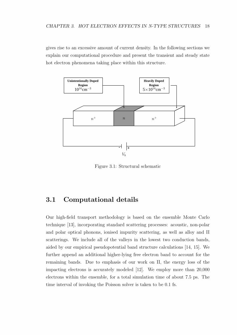
CHAPTER 3. HOT ELECTRON EFFECTS IN N-TYPE STRUCTURES 18
gives rise to an excessive amount of current density. In the following sections we
explain our computational procedure and present the transient and steady state
hot electron phenomena taking place within this structure.
+-
Vb
n+ n n
+
Unintentionally DopedRegion
1016cm−3
Heavily DopedRegion
5×1018cm−3
Figure 3.1: Structural schematic
3.1 Computational details
Our high-field transport methodology is based on the ensemble Monte Carlo
technique [13], incorporating standard scattering processes: acoustic, non-polar
and polar optical phonons, ionised impurity scattering, as well as alloy and II
scatterings. We include all of the valleys in the lowest two conduction bands,
aided by our empirical pseudopotential band structure calculations [14, 15]. We
further append an additional higher-lying free electron band to account for the
remaining bands. Due to emphasis of our work on II, the energy loss of the
impacting electrons is accurately modeled [12]. We employ more than 20,000
electrons within the ensemble, for a total simulation time of about 7.5 ps. The
time interval of invoking the Poisson solver is taken to be 0.1 fs.

CHAPTER 3. HOT ELECTRON EFFECTS IN N-TYPE STRUCTURES 19
3.2 Alloy scattering
The subject of alloy scattering has caused substantial controversy over the years
which is still unsettled. In the case of group-III nitrides, Farahmand et al. [16]
have dealt with this issue and reported that using the conduction band offset
between the binary constituents as the alloy potential leads to an upper bound
for alloy scattering. Being more conservative, for this value we prefer to use
0.91 eV, which is half of the corresponding GaN/AlN conduction band offset.
Another source of concern has to do with the particular implementation of alloy
scattering within the Monte Carlo simulation. Following Fischetti and Laux [17],
we treat the alloy scattering as an intra-valley process with the distribution of
the final scattering angles assumed to be isotropic, even though at higher energies
it attains a forward directional character which should presumably weaken the
effect of this mechanism on the momentum relaxation. Therefore, we are led to
think that the effect of alloy scattering may still be overestimated.
0.0 0.1 0.2 0.3 0.4 0.5 0.60
1
2
3
4
5
6
5x1018 cm-35x1018 cm-3
Al0.4
Ga0.6
N
AlN
GaN
N N+N+
aver
age
velo
city
(10
7 cm/s
)
distance (µm)
Figure 3.2: Velocity distribution over the n+ − n − n+ channel under an appliedbias of 20 V.

CHAPTER 3. HOT ELECTRON EFFECTS IN N-TYPE STRUCTURES 20
3.3 Results
To gain insight into the high-field transport phenomena in GaN, AlN or
AlxGa1−xN based sub-micron sized dimensions we consider a simple n+ −n−n+
homojunction channel device [18] having 0.1 µm-thick unintentionally doped (1016
cm−3) n region sandwiched between two heavily doped (5× 1018 cm−3) n+ regions
of thickness at least 0.2 µm thick; cf. Fig. 3.1. In Fig. 3.2 we show the veloc-
ity profiles for these materials; the Al0.4Ga0.6N based structure suffers severely
from alloy scattering and has a much reduced velocity. If we turn off the alloy
scattering, then the curve for Al0.4Ga0.6N (not shown) almost coincides with that
of GaN. As a matter of fact, our previous analysis for bulk AlGaN alloys has
identified the alloy scattering to modify the high energy electron distribution and
lead to an increased II threshold [12].
0.1 0.2 0.3 0.4 0.50.0
0.5
1.0
1.5
2.0
2.5
3.0
3.5
4.0
4.5
N N+N+
GaN
elec
tric
fiel
d (M
V/c
m)
distance (µm)
50 V 40 V 30 V 20 V 10 V 5 V
Figure 3.3: Electric field distribution over the n+−n−n+ GaN channel at appliedbiases ranging from 5 V to 50 V.
The electric field along this device is distributed highly non-uniformly, reach-
ing a few MV/cm values, which peaks at the right nn+ interface, as shown in

CHAPTER 3. HOT ELECTRON EFFECTS IN N-TYPE STRUCTURES 21
Fig. 3.3 and Fig. 3.5 (a).
0.1 0.2 0.3 0.4 0.5 0.6
0
1
2
3
4
5
6
7
7.5 ps
2 ps
1 ps
0.8 ps
0.6 ps0.4 ps
N N+N+
elec
tron
den
sity
(10
18cm
-3)
distance (µm)
Figure 3.4: Time evolution of the transient electron density profile over the n+ −n − n+ GaN channel under an applied bias of 50 V; steady state result is alsoshown, evaluated at 7.5 ps.
Also note the penetration of the electric field into the heavily doped anode
n+ region with increasing applied bias, which amounts to widening of the unin-
tentionally n-doped ”base” region as in the Kirk effect; following Figures further
support this viewpoint. The time evolution of the electron density profile is de-
picted in Fig. 3.4 starting from 0.4 ps. Oscillations around the unintentionally
doped n region are clearly visible until steady state is established (7.5 ps curve
in Fig. 3.4).
The fermionic degeneracy effects are seen to be operational at high fields and
at high concentration spots. We make use of the Lugli-Ferry recipe [19] to account
for degeneracy. However, if degeneracy is ignored, the electron distribution is
observed to develop a dip in the n+ anode region, shown in Fig. 3.5(a)
At a higher applied bias (80 V in GaN) the effect of II becomes dominant.
As illustrated in Fig. 3.5 (b), this mechanism introduces a substantial energy loss
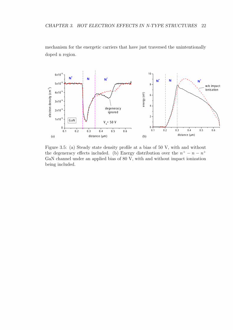
CHAPTER 3. HOT ELECTRON EFFECTS IN N-TYPE STRUCTURES 22
mechanism for the energetic carriers that have just traversed the unintentionally
doped n region.
0.1 0.2 0.3 0.4 0.5 0.60
1x10¹⁸
2x10¹⁸
3x10¹⁸
4x10¹⁸
5x10¹⁸
6x10¹⁸
Vb= 50 VGaN
N N+N+
degeneracyignored
elec
tron
dens
ity(c
m-3)
distance (µm)
0.1 0.2 0.3 0.4 0.5 0.60
2
4
6
8
10
w/o impactionisation
N+N+ N
ener
gy(e
V)
distance (µm)(a) (b)
Figure 3.5: (a) Steady state density profile at a bias of 50 V, with and withoutthe degeneracy effects included. (b) Energy distribution over the n+ − n − n+
GaN channel under an applied bias of 80 V, with and without impact ionizationbeing included.

Chapter 4
AlGaN solar-blind avalanche
photodiodes
Achieving ultraviolet solid-state photodiodes having internal gain due to
avalanche multiplication is a major objective with a potential to replace pho-
tomultiplier tube based systems for low-background applications1 [20]. The
AlxGa1−xN material with the Aluminium mole fraction, x ≥ 0.38 becomes a natu-
ral candidate for the solar-blind avalanche photodiode (APD) applications which
can also meet high-temperature and high-power requirements. Unfortunately,
due to growth-related problems, such as high defect and dislocation densities
causing premature microplasma breakdown, there has been as yet no experimen-
tal demonstration of an APD with the AlxGa1−xN material. As a matter of fact,
even for the relatively mature GaN-based technology, few reports of observation
of avalanche gain exist [21, 22, 23, 24].
While the material quality is being gradually improved, our aim in this chap-
ter is to meet the immediate demand to explore the prospects of (Al)GaN based
APDs from a computational perspective. Within the last decade, several tech-
niques have been reported which model gain and time response of APDs. Most,
1The contents of this chapter has been recently published in Applied Physics Letters [5].
23

CHAPTER 4. ALGAN SOLAR-BLIND AVALANCHE PHOTODIODES 24
however, approximate the carriers as always being at their saturated drift veloc-
ity and impact ionization rates are usually assumed to depend only on the local
electric field; for references, see Ref. [25]. While nonlocal effects have recently
been incorporated [26], the dubious assumption on carrier drift velocity remains.
Among all possible techniques, the ensemble Monte Carlo (EMC) method is po-
tentially the most powerful as it provides a full description of the particle dy-
namics. However, only a small number of such simulations have been reported,
predominantly on GaAs based APDs [27, 28].
4.1 Computational details
As mentioned several times before, for the high-field transport phenomena, the
EMC technique is currently the most reliable choice, free from major simplifica-
tions [29]. All standard scattering mechanisms are included in our EMC treat-
ment other than dislocation, neutral impurity and the piezoacoustic scatterings as
they only become significant at low temperatures and fields [30]. Impact ioniza-
tion parameters for bulk GaN are extracted from a recent experiment of Kunihiro
et al. [31]. As for the case of AlN, due to lack of any published results, we had
to resort to a Keldysh approach, while Bloch overlaps were taken into account
via the f -sum rule [10]; for details, see Ref. [12]. Furthermore, the polar opti-
cal phonon and ionized impurity potentials are screened by using random phase
approximation based dielectric function [32].
The band structures for GaN and AlN are obtained using the empirical pseu-
dopotential technique fitted to available experimental results and first principles
computations [14, 15]. For the alloy, AlxGa1−xN, we resort to linear interpola-
tion (Vegard’s Law) between the pseudopotential form factors of the constituent
binaries. The necessary band edge energy, effective mass and non-parabolicity
parameters of all valleys in the lowest two conduction bands and valence bands
located at high symmetry points are extracted through the computed bands of
GaN and AlxGa1−xN. To account for the remaining excited conduction and va-
lence bands, we further append additional higher-lying parabolic free electron and

CHAPTER 4. ALGAN SOLAR-BLIND AVALANCHE PHOTODIODES 25
hole bands. At this point it is important to stress that we use the actual density
of states computed using the Lehmann-Taut approach [9], rather than the valley-
based non-parabolic band approximation, in calculating the scattering rates [33].
This assures perfect agreement with rigorous full-band EMC simulations [34] even
for the hole drift velocities at a field of 1 MV/cm.
During the computation the Schottky barrier height is neglected in compar-
ison to the applied very high reverse bias, whereas, it needs to be included in
the case of a forward bias. Similarly, this eliminates the subtle complications re-
garding the choice of a suitable boundary condition, hence, we use the standard
neutral-contact model which keeps the charge density constant at the boundary
regions via injecting or removing majority/minority carriers. To decrease the sta-
tistical noise on the current, we employ more than 60,000 superparticles within
the ensemble, and use the higher-order triangular-shaped-cloud representation of
the superparticle charge densities [35]. The Poisson solver is invoked in 0.25 fs
time intervals not to cause an artificial plasma oscillation. All computations are
done for a temperature of 300 K. To avoid prolonged transients following the
sudden application of a high-field, the reverse DC bias is gradually applied across
the APD over a linear ramp within the first 1.25 ps.
Vb
n+
n
p+ ⊕
⊕
hν
OpticalPump
Impactionization
Figure 4.1: Structural details.

CHAPTER 4. ALGAN SOLAR-BLIND AVALANCHE PHOTODIODES 26
4.2 Results
In the following subsections, we only deal with the gain and temporal response
of the GAN and AlGaN APDs. Other important properties, such as noise and
spectral response are not included in this work.
4.2.1 GaN APDs
Even though, our principal aim is to characterize solar-blind APDs attainable
with the band gap of Al0.4Ga0.6N, we first test the performance of our method-
ology on GaN-based visible-blind APDs where a few experimental results have
recently been reported [21, 22, 23, 24]. Among these, we choose the structure
(Fig. 4.1) reported by Carrano et al. [23] having 0.1 µm thick unintentionally
doped (1016 cm−3) n (multiplication) region sandwiched between 0.2 µm thick
heavily doped (1018 cm−3) p+ region and a heavily doped (1019 cm−3) n+ region.
Fig. 4.2(a) shows that the current gain of this structure where, following Carrano
20 40 60 800
2
4
6
8
10
0 10 20 30 40 500
1
2
3
4
5
GaN Al0.4
Ga0.6
N
w/o Alloyscattering
Gai
n
Voltage (V)(b)(a)
EMC
Measured
Gai
n
Voltage (V)
Figure 4.2: (a) Current gain of the GaN APD; EMC simulation (symbols) com-pared with measurements [23] (dotted). (b) Current gain of the Al0.4Ga0.6N APDsimulated using EMC with and without alloy scattering. Full lines in EMC curvesare used to guide the eye.

CHAPTER 4. ALGAN SOLAR-BLIND AVALANCHE PHOTODIODES 27
et al., the current value at 1 V is chosen as the unity gain reference point. The
overall agreement between EMC and the measurements [23] is reasonable. No-
tably, EMC simulation yields somewhat higher values over the gain region, and
the breakdown at 51 V cannot be observed with the simulations. Nevertheless,
given the fact that there is no fitting parameter used in our simulation, we find
this agreement quite satisfactory.
An important characteristic of the APDs is their time response under an
optical pulse. For this purpose, an optical pump is turned on at 6.25 ps creating
electron-hole pairs at random positions consistent with the absorption profile of
the electromagnetic radiation with a skin depth value of 10−5 cm for GaN. The
photon flux is assumed to be such that an electron-hole pair is created in 0.5 fs
time intervals. The optical pump is kept on for 25 ps to assure that steady state
is attained and afterwards it is turned off at 31.25 ps to observe the fall of the
current. As we are assuming a p-side illumination, it is mainly the electrons
which travel through the multiplication region, even though in the simulation the
impact ionization of both electrons and holes are included.
The falling edge of the optical pulse response can be fitted with a Gaussian
profile exp(−t2/τ 2f ), see parameters in Table 4.1. As seen in Fig. 4.3 and Table 4.1,
Table 4.1: Fitted temporal response functions exp(−t2/τ 2f ) and 1 −
exp(−t2/τ 2r ) cos(ωrt) for the GaN APD.
Bias (V) τf (ps) τr (ps) ωr (r/ps)25 1.72 3.06 0.3530 1.78 2.57 0.3840 2.04 1.75 0.506
the width of the Gaussian profile increases with the applied bias. Hence, the
temporal response of the device degrades in the high gain region where substantial
amount of secondary carriers exist, as expected. The rising edge of the pulse shows
an underdamped behavior, becoming even more pronounced towards the gain
region; this can approximately be fitted by a function 1 − exp(−t2/τ 2r ) cos(ωrt),
with the parameters being listed in Table 4.1.

CHAPTER 4. ALGAN SOLAR-BLIND AVALANCHE PHOTODIODES 28
5 10 15 20 25 30 350.0
1.5
3.0
4.5
Cur
rent
(A
rbitr
ary
Uni
ts)
Time (ps)
w/o alloyscattering
30 V
Al0.4
Ga0.6
N
25 V
30 V
40 V
GaN
Figure 4.3: Temporal response of the GaN and Al0.4Ga0.6N (vertically shifted forclarity) APD to a 25 ps optical pulse, applied between the dashed lines.
Fig. 4.4(a) demonstrates the electric field profile of the GaN APD. Observe
that as the applied bias increases the moderately doped p+ region becomes vul-
nerable to the penetration of the electric field, hence preventing further building
up in the multiplication region and increasing the impact ionization events. In
this regard, it needs to be mentioned that achieving very high p doping persists
as a major technological challenge. Therefore, in our considerations to follow for
the AlGaN APDs, we replace the problematic p+ region with a Schottky contact.
4.2.2 Schottky contact-AlGaN APDs
With this insight, we analyze an Al0.4Ga0.6N APD of 0.1 µm thick unintentionally
doped (1016 cm−3) n region sandwiched between a Schottky contact and a heavily
doped (1019 cm−3) n+ region.
Previously, in unipolar AlGaN structures we observed the alloy scattering to
be substantial (Chapter 3)[4], whereas the actual significance of this mechanism
CHAPTER 4. ALGAN SOLAR-BLIND AVALANCHE PHOTODIODES 29
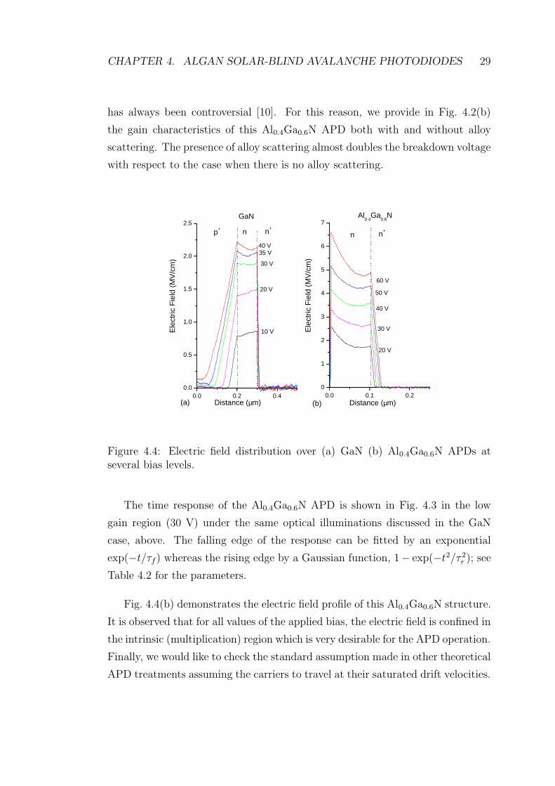
has always been controversial [10]. For this reason, we provide in Fig. 4.2(b)
the gain characteristics of this Al0.4Ga0.6N APD both with and without alloy
scattering. The presence of alloy scattering almost doubles the breakdown voltage
with respect to the case when there is no alloy scattering.
0.0 0.2 0.40.0
0.5
1.0
1.5
2.0
2.5
0.0 0.1 0.20
1
2
3
4
5
6
7
p+
nn n+n+
40 V35 V
30 V
20 V
10 VEle
ctric
Fie
ld (
MV
/cm
)
Distance (µm) (b)(a)
60 V
50 V
40 V
30 V
20 V
Al0.4
Ga0.6
NGaN
Ele
ctric
Fie
ld (
MV
/cm
)
Distance (µm)
Figure 4.4: Electric field distribution over (a) GaN (b) Al0.4Ga0.6N APDs atseveral bias levels.
The time response of the Al0.4Ga0.6N APD is shown in Fig. 4.3 in the low
gain region (30 V) under the same optical illuminations discussed in the GaN
case, above. The falling edge of the response can be fitted by an exponential
exp(−t/τf ) whereas the rising edge by a Gaussian function, 1− exp(−t2/τ 2r ); see
Table 4.2 for the parameters.
Fig. 4.4(b) demonstrates the electric field profile of this Al0.4Ga0.6N structure.
It is observed that for all values of the applied bias, the electric field is confined in
the intrinsic (multiplication) region which is very desirable for the APD operation.
Finally, we would like to check the standard assumption made in other theoretical
APD treatments assuming the carriers to travel at their saturated drift velocities.

CHAPTER 4. ALGAN SOLAR-BLIND AVALANCHE PHOTODIODES 30
Table 4.2: Fitted temporal response functions exp(−t/τf ) and 1 − exp(−t2/τ 2r )
for Al0.4Ga0.6N APD under a reverse bias of 30 V.
Alloy Scattering τf (ps) τr (ps)No 0.75 0.67Yes 1.06 2.14
It is seen in Fig. 4.5 that this assumption may be acceptable for the Schottky
structure having a uniform field distribution within the multiplication region,
whereas it is not appropriate in the p+ − n − n+ case with our doping values.
Also it should be noted that, some of the wild oscillations in the n-region of
Fig. 4.5(a) are possibly due to poor statistical averaging of our EMC simulation2.
0.0 0.1 0.2 0.3 0.40.0
1.3x10⁷
2.5x10⁷
3.8x10⁷
5.0x10⁷
0.00 0.05 0.10 0.15 0.200.0
5.0x10⁶
1.0x10⁷
1.5x10⁷
n+np+
Vel
ocity
(cm
/s)
Distance (µm) (b)(a)
n+n
70 V40 VAl
0.4Ga
0.6NGaN
Vel
ocity
(cm
/s)
Distance (µm)
Figure 4.5: Average velocity distribution over (a) GaN (b) Al0.4Ga0.6N APDs forelectron (solid) and holes (dotted).
2This point has been kindly brought to our attention by Prof. Cengiz Besikci.

CHAPTER 4. ALGAN SOLAR-BLIND AVALANCHE PHOTODIODES 31
Any experimental support, which is currently impeded by the poor AlGaN
material quality, will be extremely valuable to further refine our models. In other
words, our simulations await to be verified or falsified by other researchers.

Chapter 5
Gunn oscillations in GaN
channels
At high electric fields, the electron velocity, v, in GaAs, GaN, AlN, and some
other compound semiconductors decreases with an increase in the electric field,
F , so that the differential mobility, µd = dv/dF becomes negative (see Fig. 5.1).
Ridley and Watkins in 1961 and Hilsum in 1962 were first to suggest that such
a negative differential mobility in high electric fields is related to an electron
transfer between different valleys of the conduction band (intervalley transfer).
When the electric field is low, electrons are primarily located in the central valley
of the conduction band. As the electric field increases many electrons gain enough
energy for the intervalley transition into higher satellite valleys. The electron
effective mass in the satellite valleys is much greater than in the central valley.
Also, the intervalley transition is accompanied by an increased electron scattering.
These factors result in a decrease of the electron velocity in high electric fields.
There are other mechanisms than the intervalley transfer to achieve negative
differential mobility as well [36]. From the technological point of view, this effect
is exploited to build oscillators up to Terahertz frequencies.
32

CHAPTER 5. GUNN OSCILLATIONS IN GAN CHANNELS 33
0 200 400 600 800 10005.0x106
1.0x10⁷
1.5x10⁷
2.0x10⁷GaN
Drif
t Vel
ocity
(cm
/s)
Electric Field (kV/cm)
Figure 5.1: EMC simulation of the drift velocity versus field for bulk GaN at300 K.
5.1 Basics
A simplified equivalent circuit [37] of a uniformly doped semiconductor may be
presented as a parallel combination of the differential resistance (see Fig. 5.2)
Rd =L
qµdn0S, (5.1)
and the differential capacitance:
Cd =εS
L. (5.2)
Here S is the cross section of the sample, L is the sample length, and n0 is the
electron concentration.
The equivalent RC time constant determining the evolution of the space
charge is given by
τmd = RdCd =ε
qµdn0
, (5.3)

CHAPTER 5. GUNN OSCILLATIONS IN GAN CHANNELS 34
Rd =L
qµdn0S
Cd =εSL
Figure 5.2: Equivalent circuit for a uniform piece of semiconductor.
where, τmd is called the differential dielectric relaxation time or Maxwell dielec-
tric relaxation time. In a material with a positive differential conductivity, a
space charge fluctuation decays exponentially with this time constant. However,
if the differential conductivity is negative, the space charge fluctuation may grow
with time. What actually happens depends on the relationship between τmd and
the electron transit time, τtr = L/v. If (-τmd) τtr, a fluctuation of the electron
concentration occurring near the negatively biased terminal (cathode) grows very
little during its transit time toward the positively biased terminal (anode). How-
ever, when (-τmd) τtr, a space charge fluctuation grows tremendously during
a small fraction of the transit time. In this case, it develops into a high-field
region (called a high-field domain), which propagates from the cathode toward
the anode with the velocity that is approximately equal to the electron saturation
velocity, vs.
The condition (-τmd) τtr leads the following criterion of a high-field domain
formation:
n0L εvs
q|µd|. (5.4)
For v = 105 m/s, |µd| ' 0.15 m2/Vs, ε = 1.14×10⁻¹⁰ F/m, we obtain n0L
1.5×1011 cm−2. This condition (first introduced by Professor Herbert Kromer
in 1965) is called the Kromer criterion. On the experimental side, Ian Gunn

CHAPTER 5. GUNN OSCILLATIONS IN GAN CHANNELS 35
was first to observe high-field domains in GaAs in 1963. Ever since, these GaAs
two-terminal devices are often called Gunn diodes
5.2 Motivation
The negative differential mobility threshold field due to intervalley carrier transfer
for GaN is quite high, above 200 kV/cm, which becomes appealing for building
very high power millimeter-wave oscillators (see Fig. 5.1). In addition to their
technological importance, these Gunn diodes still pose a number of physical puz-
zles, such as the detailed understanding of the domain nucleation process in
different doping profiles [38]. Also, the onset of chaotic behavior [39] in these
structures is another intriguing subject. As a matter of fact, the presence of im-
pact ionization has been reported to give rise to chaotic multi-domain formation
[40]. This result was based on a numerical solution of a set of partial differential
equations under simplifying assumptions. The ensemble Monte Carlo (EMC) ap-
proach is believed to be much better suited for this task [41], and, for instance,
it has been successfully tested in the analysis of InP Gunn diodes [42].
An ever-present objective is to increase the operating frequency of the Gunn
diodes. This can be achieved in several ways. Our approach is to operate the
Gunn diodes at their higher harmonic frequencies rather than the fundamental.
However, the drawback here is the very low efficiency associated with these high
harmonic modes. Therefore, we devote much of this chapter to the harmonic RF
conversion efficiency enhancement by all means.

CHAPTER 5. GUNN OSCILLATIONS IN GAN CHANNELS 36
Active Region
3×1017cm−3
Unintentionally DopedNotch Region
1016cm−3
Heavily DopedRegion
2×1018cm−3
n+
n− n n
+
+-
Vb
Figure 5.3: Structural details.
5.3 Computational details
Along this line, here we employ the EMC method to shed light on the dynam-
ics of millimeter-wave Gunn domain oscillations with large amplitudes in GaN
channels. The same GaN material was the subject of another recent study with
an emphasis on multiple-transit region effects on the output power [43]. Unfor-
tunately, their analysis utilized unrealistic values for the two important satellite
valleys, chosen as 2.27 eV and 2.4 eV above the conduction band edge. These are
about 1 eV higher than the experimental and theoretical values. In this work,
as mentioned before, the necessary band structure data is extracted from our
empirical pseudopotential calculations [14] fitted to available experimental and
theoretical data. An analytical-band variant of EMC is preferred that enables a
vast number of simulations. Very good agreement of such an approach with full
band EMC results [44] gives further confidence for this choice. Moreover, we use
the actual density of states, rather than the valley-based non-parabolic bands in

CHAPTER 5. GUNN OSCILLATIONS IN GAN CHANNELS 37
forming the scattering tables [45].
The basic structure we investigate is of the form, n+ − n− − n− n+, with the
active region being formed by the n− notch with a doping of 1016 cm−3 and the
main n-doped channel having 3×1017 cm−3 doping; the n+ contact regions are
assumed to have 2×1018 cm−3 dopings; see, Fig 5.3. The length of the notch region
is varied to investigate its effect on the harmonic operation, while keeping the total
length of the active region (n−−n) constant at 1.2 µm. Our EMC simulations all
start from a neutral charge distribution, and unless otherwise stated, are at 300
K. As a standard practice in modeling Gunn diodes (see, Ref. [38] and references
therein), a single-tone sinusoidal potential of the form VDC+VAC sin(2πft) is
imposed across the structure; in our work VDC=60 V and VAC=15 V (if not
stated). This choice significantly simplifies our frequency performance analysis;
its validity will be checked later on. The oscillator efficiency is defined as η
= PAC/PDC , where PAC is the time-average generated AC power and PDC is
the dissipated DC power by the Gunn diode. Therefore, a negative efficiency
corresponds to a resistive (dissipative) device and a positive value designates an
RF conversion from DC.
5.4 Results
Fig. 5.4(a) displays Gunn domains for operations at the fundamental, second,
third and fourth harmonic frequencies for a 250 nm notch device1. As usual,
the domains build up as they approach to the anode side. Fig. 5.4(b) illustrates
the evolution of the electric field in one period for the fundamental frequency
operation (122.5 GHz). It can be noted that due to the relatively wide notch
width, significant amount of the electric field accumulates around this region,
with a value that can exceed 1.2 MV/cm (under a DC bias of 60 V), reaching
impact ionization threshold [12]. To analyze this further, we increased the DC
bias to 90 V and the operating temperature to 500 K; the effect of turning off the
impact ionization mechanism was observed to be marginal even at these extreme
1A part of this section will be published in Semiconductor Science and Technology.

CHAPTER 5. GUNN OSCILLATIONS IN GAN CHANNELS 38
conditions for all notch widths considered.
0.0 0.2 0.4 0.6 0.8 1.0 1.2 1.4 1.60.0
0.4
0.8
1.2
1.60.2 0.4 0.6 0.8 1.0 1.2
0
2
4
6
t ps t+2 ps t+4 ps t+6 ps
Fie
ld (
MV
/cm
)
Distance (µm)
(b)
(a)
Cha
rge
Den
sity
(10
18cm
-3)
Distance (µm)
Figure 5.4: (a) Typical charge density profiles for a 250 nm-notch device operat-ing at the fundamental, second, third, fourth-harmonic modes, each respectivelyvertically up-shifted for clarity. (b) Time evolution of the electric field profilewithin one period of the Gunn oscillation at 2 ps intervals for the 250 nm-notchdevice.
5.4.1 The effect of notch width
In Fig. 5.5(a) different notch widths are compared in terms of their frequency
performance. Our main finding is that, by increasing the notch width, GaN Gunn
diodes can be operated with more efficiency at their second harmonic frequency
than the fundamental, as seen for the 250 nm notch-width curve. However, we
observed that further increasing the notch width above 400 nm gives rise to total
loss of the Gunn oscillations. These results are extracted from long simulations

CHAPTER 5. GUNN OSCILLATIONS IN GAN CHANNELS 39
up to 500 ps to capture the steady state characteristics at each frequency, which
becomes quite demanding. Hence, the Pauli degeneracy effects requiring extensive
memory storage are not included. Fig. 5.5(b) illustrates the effect of including the
Pauli exclusion principle using the Lugli-Ferry recipe [19, 4]. Note that for Gunn
diodes, this effect is quite negligible, slightly lowering the resonance frequencies
at higher harmonics.
100 200 300 400 500 600 700
-1
0
1
100 200 300 400 500 600 700-2
-1
0
1
Notch : 250 nm
with Pauli Exc.
w/o Pauli Exc.
(a)
Effi
cien
cy (
%)
Frequency (GHz)
Notch : 80 nm150 nm
250 nm
(b)
Effi
cien
cy (
%)
Frequency (GHz)
Figure 5.5: Gunn diode efficiency versus frequency. (a) Effect of different doping-notch widths, while keeping the total active channel length fixed at 1.2 µm. (b)Effect of including the Pauli exclusion principle for the 250 nm-notch device.

CHAPTER 5. GUNN OSCILLATIONS IN GAN CHANNELS 40
5.4.2 The effect of lattice temperature
Being a unipolar device, Gunn diodes operate under high current levels which
leads to excessive heating of the lattice. Therefore, we would like to consider
the effects of temperature on our results, picking 250 nm-notch device (being the
most promising one in harmonic enhancement). As seen in Fig. 5.6, in response to
an increase in the lattice temperature, second harmonic efficiency increases where
as the fundamental and third harmonic efficiencies decrease. Also, as expected
the curves shift to lower frequencies due to increased phonon scattering which
reduces the carrier saturation velocity and hence the Gunn oscillation frequency.
The important finding is that at even higher lattice temperatures the second-
harmonic efficiency is further reinforced.
100 200 300 400 500 600-1.5
-1.0
-0.5
0.0
0.5
1.0
1.5
2.0
Notch = 250 nm & 60 V600 K
400 K
300 K
Eff
icie
ncy
(%)
Frequency (GHz)
Figure 5.6: RF conversion efficiency versus frequency for several lattice temper-atures; 250 nm-notch device at 60 V bias is used.

CHAPTER 5. GUNN OSCILLATIONS IN GAN CHANNELS 41
5.4.3 The effect of channel doping
Next, we consider the effect of the channel doping again using the same 250 nm-
notch device for comparison purposes. One can easily observe from Fig. 5.7 that
the channel doping is highly critical in the operation of the Gunn diodes. This
doping is mainly instrumental in the differential dielectric relaxation time (see
Eq. 5.3) which decreases as the doping increases. For relatively low channel
dopings, the −τmd τtr condition gets violated which explains the behavior
displayed in Fig. 5.7. Furthermore, at lower channel dopings, not only the AC
current magnitude is decreased but also the phase angle difference with respect
to AC voltage shifts from active toward lossless and dissipative regimes. If the
channel doping is increased beyond 3 × 1017 cm−3 than the part of the active
channel on the anode side begins to act like a contact, reducing the dimension of
the active channel length, hence increasing the Gunn oscillation frequency.
100 200 300 400 500 600
-1.5
-1.0
-0.5
0.0
0.5
1.0
1.5
Notch = 250 nm
1 x 10¹⁷
5 x 10¹⁶
3 x 10¹⁷
Effi
cien
cy (
%)
Frequency (GHz)
Figure 5.7: RF conversion efficiency versus frequency for several channel dopings;250 nm-notch device at 60 V bias is used.

CHAPTER 5. GUNN OSCILLATIONS IN GAN CHANNELS 42
5.4.4 The effect of DC operating point
Another parameter that can affect the achievement of harmonic enhancement is
the DC operating point. Not to lose the grounds for comparison, we need to
scale the RF amplitude while changing the applied DC voltage across the Gunn
diode. Hence, we simulate the same 250 nm-notch Gunn diodes operating under
three different DC and RF bias levels which are 50 V DC bias with 12.5 V RF
bias, 60 V DC bias with 15 V RF bias, 70 V DC bias with 17.5 V RF bias. The
important observation is that the harmonic enhancement is favored towards the
critical field at which negative differential mobility sets in (50 V case in Fig. 5.8).
100 200 300 400 500 600-1.5
-1.0
-0.5
0.0
0.5
1.0
1.5
Notch = 250 nm
70 V DC, 17.5 V RF 60 V DC, 15 V RF 50 V DC, 12.5 V RF
Effi
cien
cy (
%)
Frequency (GHz)
Figure 5.8: RF conversion efficiency versus frequency for several DC bias voltages;250 nm-notch device.

CHAPTER 5. GUNN OSCILLATIONS IN GAN CHANNELS 43
5.4.5 Connecting to a tank circuit
Finally, we relax the imposed single-tone sinusoidal voltage across the Gunn diode
and connect it to an external tank circuit with the voltage across the device being
self-consistently updated at each simulation step (0.4 fs) through solving in time-
domain a Gunn diode in parallel with a capacitor and a resistor, all in series with
an inductor and a DC source (cf. Fig. 5.9(b) inset). The AC voltage and current
of the Gunn diode are shown in Figs. 5.9(a) and (b), comparing respectively the
imposed single-tone bias with the tank circuit tuned to the fundamental frequency
of the 150 nm notch device. For both cases the current and voltage are in anti-
phase with each other leading to RF generation as intended; the main discrepancy
being higher harmonic content in the tank circuit case as governed by the quality
factor of the resonator.
Notch = 150 nm
150 160 170Time (ps)
with an External Tank Circuit
Under Single-Tone Sinusoidal Bias
CurrentVoltageGunn
R
C
L
+ -
(b)
(a)
Figure 5.9: Current and voltage waveforms for a 150 nm-notch Gunn diode (a)under an imposed single-tone sinusoidal voltage, and (b) connected to an externaltank circuit shown in the inset.

CHAPTER 5. GUNN OSCILLATIONS IN GAN CHANNELS 44
5.5 Computational budget
Finally, we would like to give some details about the computational load of our
simulations. All of our computations have been carried on a dedicated Pentium-
4 3.06 GHz PC running on a Linux (RedHat v8.0) operating system, complied
with the most recent Intel 7.1 Fortran complier. To give some idea, the Gunn
simulations of this chapter have been completed in about 3.5 months non-stop.
The memory requirement of a typical run is less than 5 Mb which increases to
1.1 Gb when Pauli exclusion principle as implemented by the Lugli-Ferry recipe
is included as in Fig. 5.5(b).

Chapter 6
Summary of the main findings
This work has been devoted to the investigation of the high field transport phe-
nomena in wide bandgap semiconductors such as (GaN, AlGaN and AlN). With
this objective, an EMC-based simulation tool has been developed. All of major
scattering mechanisms have been added, capable of simulating both electrons and
holes, within unipolar/bipolar diode structures.
First, we considered GaN, AlGaN and AlN based unipolar homojunction chan-
nel devices to gain insight to the high-field transport phenomena. We examined
the velocity, electric field profiles and time evolution of the electron density in
these materials. Our first finding was that the Al0.4Ga0.6N-based structures suffer
severely from alloy scattering and possess a much reduced drift velocity. When
we turned off the alloy scattering, the curve for Al0.4Ga0.6N has almost coincided
with that for GaN. The electric field profile along this device was distributed
highly non-uniformly, reaching a values of few MV/cm, peaking at nn+ inter-
face and also penetrating into the heavily doped anode n+-region as the applied
bias is increased. In time evolution of the electron density oscillation around the
unintentionally doped n-region were observed until steady state is established.
Fermionic degeneracy effects were seen to be operational at high fields and high
concentration spots. At very high fields II was shown to introduce a substantial
energy loss mechanisms for the energetic carriers that have just traversed the
unintentionally doped n-region.
45

CHAPTER 6. SUMMARY OF THE MAIN FINDINGS 46
Next, we analyzed multiplication and temporal response characteristic of GaN
and Schottky Al0.4Ga0.6N APDs. To check our model, we simulated the structure
reported by Carrano et al. [23] and obtained reasonable agreement. Examining
the time response of APDs under a pico-second optical illumination, an under-
damped step response was observed in the rising edge and a Gaussian profile
damping in the falling edge. For the electric profile of the GaN APD, we noted
that as the applied bias increases the electric field increases along the p+ region.
To increase the electric field at the multiplication region, we replaced the prob-
lematic p+-region with a Schottky contact and simulated the Schottky-contact
Al0.4Ga0.6N APD. As intended, for all values of the applied bias, the electric field
was observed to be confined in the multiplication region. For the gain characteris-
tics of Schottky contact Al0.4Ga0.6N APD both with and without alloy scattering
and we found that the presence of alloy scattering doubles the breakdown voltage.
Finally, we studied the Gunn domain oscillations under both impressed single-
tone sinusoidal bias and external tank circuit conditions. In particular, our mo-
tivation was to seek all means to enhance the harmonic RF conversion in com-
parison to the fundamental mode operation. Hence, we examined the effect of
the notch width on the higher harmonic frequencies and found that GaN Gunn
diodes can be operated with more efficiency at their second harmonic frequency
for wide-enough notch regions. However, there exists an upper limit the width
of this region beyond which Gunn oscillations ceases altogether. Moreover, the
Pauli degeneracy effect and impact ionization scattering were seen to be quite
negligible. Furthermore, increasing the lattice temperature or the channel dop-
ing was observed to enhance the second harmonic efficiency. Finally, we studied
the Gunn diodes operating under different DC bias levels; the fundamental mode
was seen to be affected by far, compared to higher harmonics.
At this point, we would like to mention some possible extension of this work.
Being a close relative of the devices considered here, IMPATT diodes can also
be studied using the some infrastructure. On the more basic research side, it is
intriguing to explore chaos in Gunn diodes [53], and other high field devices. From
a technical perspective, other scattering mechanisms can be included such as the
carrier-carrier scattering, and for low temperature and poor quality samples the

CHAPTER 6. SUMMARY OF THE MAIN FINDINGS 47
dislocation scattering. Finally, the code can be upgraded to a fullband EMC [54]
and even employing ab-initio bandstructure techniques rather than the EPM.
However, our current analytical-band EMC tool will still preserve its place, as it
is still the preferred choice for extensive simulations to test certain ideas, as we
have done in pursing the harmonic enhancement in Gunn diodes.

Bibliography
[1] M. Shur, Solid-State Electron. 42, 2119 (1998).
[2] M. Razeghi, A. Rogalski, J. Appl. Phys. 79, 7433 (1996).
[3] C. Jacoboni and L. Reggiani, Reviews of Modern Physics, 55, 645 (1983).
[4] C. Sevik and C. Bulutay IEE Proc.-J: Optoelectron. 150, 86 (2003).
[5] C. Sevik and C. Bulutay Appl. Phys. Lett. 83, 1382 (2003).
[6] M. Lundstrom, Fundamentals of Carrier Transport, 2nd ed. (Cambridge
University Press, 2000).
[7] K. Tomizawa, Numerical Simulation of submicron Semiconductor Devices
( Artech House, 1993).
[8] C. Sevik and C. Bulutay, to be published in Semicond. Sci. Technol.
[9] G. Lehmann and M. Taut, Phys. Status Solidi B 54, 469 (1972).
[10] D. K. Ferry, Semiconductor Transport (Taylor and Francis, 2000).
[11] A. D. Boardman (editor), Physics Programs (Wiley, 1980).
[12] C. Bulutay, Semicond. Sci. Technol. 17, L59 (2002).
[13] W. Fawcett, A. D. Boardman andS. J. Swain, Phys. Chem. Solids 31, 1963
(1970).
[14] C. Bulutay, B. K. Ridley, and N. A. Zakhleniuk, Phys. Rev. B 62, 15754
(2000).
48

BIBLIOGRAPHY 49
[15] C. Bulutay, B. K. Ridley, and N. A. Zakhleniuk, Physica B 314, 63 (2002).
[16] M. Farahmand, C. Garetto, E. Bellotti,K. F. Brennan, M. Goano, E.
Ghillino, G. Ghione, J. D. Albrecht and P. P. Ruden, IEEE Trans. Electron
Devices 48, 535 (2001).
[17] M. V. Fischetti and S. E. Laux, J. Appl. Phys. 80, 2234 (1996).
[18] K. Tomizawa, Y. Awano, N. Hashizume and M. Kawashima, IEE Proc.
129, 131 (1982).
[19] P. Lugli and D. K. Ferry IEEE Trans. Electron Devices 32, 2431 (1985).
[20] M. Razeghi, Proc. IEEE 90, 1006 (2002).
[21] A. Osinsky, M. S.Shur, R. Gaska, and Q. Chen, Electron. Lett. 34, 691
(1998).
[22] K. A. McIntosh, R. J. Molnar, L. J. Mahoney, A. Lightfoot, M. W. Geis,
K. M. Molvar, I. Melngailis, R. L. Aggarwal, W. D. Goodhue, S. S. Choi,
D. L. Spears, S. Verghese, Appl. Phys. Lett. 75, 3485 (1999).
[23] J. C. Carrano, D. J. H. Lambert, C. J. Eiting, C. J. Collins, T. Li, S. Wang,
B. Yang, A.L. Beck, R.D. Dupuis, J. C. Campbell, Appl. Phys. Lett. 88,
924 (2000).
[24] B. Yang, T. Li, K. Heng, C. Collins, S. Wang, J. C. Carrano, R. D. Dupuis,
R. C. Campbell, M. J. Schurman, and I. T. Ferguson, IEEE J. Quantum
Electron. 36, 1389 (2000).
[25] P. J. Hambleton, S. A. Plimmer, J. P. R. David, G. J. Rees, and G. M.
Dunn, J. Appl. Phys. 91, 2107 (2002).
[26] K. F. Li, D. S. Ong, , J. P. R. David, G. J. Rees, R. C. Tozer, P. N. Robson,
and R. Grey, IEEE Trans. Electron Devices 45, 2102 (1998).
[27] G. M. Dunn, G. J. Rees, J. P. R. David, S. A. Plimmer, and D. C. Herbert,
Semicond. Sci. Technol. 12, 111 (1997).

BIBLIOGRAPHY 50
[28] F. Ma, S. Wang, X. Li, K. A. Anselm, X. G. Zheng, A. L. Holmes, and J.
C. Campbell, J. Appl. Phys. 92, 4791, (2002).
[29] D. Vasileska and S. M. Goodnick, Mat. Sci Eng. R 38,181 (2002).
[30] B. K. Ridley, Quantum Processes in Semiconductors, 4th ed. (Oxford Uni-
versity Press, 1999).
[31] K. Kunihiro, K. Kasahara, Y. Takahashi, and Y. Ohno, IEEE Electron
Device Lett. 20 608 (1999).
[32] M. A. Osman and D. K. Ferry, Phys. Rev. B 36, 6018 (1987).
[33] M. V. Fischetti and J. M. Higman, Monte Carlo Device Simulation: Full
Band and Beyond, edited by K. Hess (Kluwer, 1991).
[34] I. H. Oguzman, J. Kolnik, and K. F. Brennan, J. Appl. Phys. 80, 8 (1996).
[35] R. W. Hockney and J. W. Eastwood, Computer Simulation Using Particles,
(Institute of Physics, 1988).
[36] N. Balkan, B. K. Ridley, and A. J. Vickers (Editors) Negative Differential
Resistance and Instabilities in 2-D Semiconductors (Plenum, 1993).
[37] M. Shur, Introduction to Electronic Devices, 1st ed. (Wiley, 1996).
[38] G. M. Dunn and M. J. Kearney Semicond. Sci. Technol. 18, 794 (2003).
[39] E. Scholl, Nonlinear Spatio-Temporal Dynamics and Chaos in Semiconduc-
tors (Cambridge University Press, 2001).
[40] K. Oshio and H. Yahata J. Phys. Soc. Jpn. 64, 1823 (1995).
[41] K. Hess, Advanced Theory of Semiconductor Devices (Prentice Hall, 1998),
207.
[42] V. Gruzinskis, E. Starikov, P. Shiktorov, L. Reggiani, and L. Varani J.
Appl. Phys. 76, 5260 (1994).
[43] R. P. Joshi, S. Viswanadha, P. Shah, and R. D. del Rosario J. Appl. Phys.
93, 4836 (2003).

BIBLIOGRAPHY 51
[44] A. Di Carlo, P. Lugli, C. Canali, R. Malik, M. Manfredi, A. Neviani, E.
Zanoni, and G. Zandler Semicond. Sci. Technol. 13, 858 (1998).
[45] M. V. Fischetti, J. M. Higman, in: Hess K (Ed.) Monte Carlo Device Sim-
ulation: Full Band and Beyond(Kluwer, 1991), 123.
[46] M. Reigrotzki, M. Dur, W. Schattke, N. Fitzer, R. Redmer, and S. M.
Goodnick Phys. Stat. Sol. 204, 528 (1997).
[47] Y. Ando, W. Contrata, N. Samoto, H. Miyamoto, K. Matsunaga, M.
Kuzuhara, K. Kunihiro, K. Kasahara, T. Nakayama, Y. Takahashi, N.
Hayama, and Y. Ohno IEEE Trans. Electron Devices 47, 1965 (2000).
[48] M. Farahmand and K. F. Brennan IEEE Trans. Electron Devices 46, 1319
(1999).
[49] H. K. Jung, H. Nakano, and T. Taniguchi Physica B 272, 244 (1999).
[50] O. Mouton, J. L. Thobel, and R. Fauquembergue J. Appl. Phys. 81, 3160
(1997).
[51] J. Bude and K. Hess J. Appl. Phys. 72, 3554 (1992).
[52] K. Yeom, J. M. Hinckley, and J. Singh J. Appl. Phys. 80, 6773 (1996).
[53] H. Ito and Y. Ueda Phys. Lett. A 280, 312 (2001).
[54] M. V. Fischetti and S. E. Laux, Phys. Rev. B 38, 9721 (1988).

Appendix A
Impact ionization and alloy
scattering
In this appendix, we would like to explain our approach for the impact ionization
(II) and alloy scattering in more detail for documentation purposes.
A.1 Impact ionization
The only available experimental report about II relevant to our work is on GaN
by Kunihiro et al. [31]. Using our EMC framework, we are able to fit to their
electron ionization coefficient with an II scattering rate of P GaNII (1/s)=2.5 × 1016
(Ein - EGaNth )8 u(Ein - EGaN
th ), where Ein is the energy of the electron in eV,
EGaNth = 4 eV is the II threshold energy, and u(·) is the unit step function1. This
expression, when compared to the ab initio results for GaN [46] possesses similar
exponent and threshold values, but a reduced coefficient. On the other side,
for AlxGa1−xN Ando et al. [47]. used linear interpolation between the II rates
of GaN and AlN, assuming for simplicity a null value for AlN. Aiming for a
more realistic estimation for AlN, we make use of the Keldysh approach valid for
parabolic bands while Bloch overlaps are taken into account via the f -sum rule
1The contents of this chapter has been adopted from Ref [12].
52

APPENDIX A. IMPACT IONIZATION AND ALLOY SCATTERING 53
Table A.1: Band edge analysis throughout the lowest two conduction bands ofAlxGa1−xN alloys: band edge energy, E, density of states effective mass, m∗, andnon-parabolicity factor, α (other than the lowest valley, two-band ~k · ~p valuesare preferred). Equivalent valley multiplicities, Nv are included as well. Notethat the ordering of the U and K valleys is interchanged at an aluminium molefraction of 0.6.
E(eV)m∗/m0
α(eV−1) GaN Al0.2Ga0.8N Al0.4Ga0.6N Al0.6Ga0.4N Al0.8Ga0.2N AlNΓ1(Nv = 1) 0 0 0 0 0 0
0.2 0.214 0.227 0.238 0.246 0.260.262 0.243 0.230 0.221 0.213 0.207
U(Nv = 6) 1.34 1.285 1.233 1.181 1.131 1.050.442 0.456 0.468 0.486 0.487 0.4950.064 0.056 0.049 0.043 0.039 0.035
K(Nv = 2) 1.59 1.444 1.307 1.179 1.057 0.90.47 0.477 0.483 0.478 0.488 0.4880.055 0.050 0.045 0.042 0.039 0.106
M(Nv = 3) 1.87 1.830 1.798 1.769 1.741 1.680.565 0.577 0.590 0.604 0.617 0.6290.035 0.030 0.026 0.023 0.020 0.017
Γ3(Nv = 3) 2.14 2.23 2.312 2.390 2.462 2.490.439 0.463 485 0.507 0.529 0.550.056 0.046 0.039 0.032 0.027 0.023
Free electronband (Nv = 1) 3.5 3.6 3.7 3.8 3.9 4
1 1 1 1 1 10 0 0 0 0 0
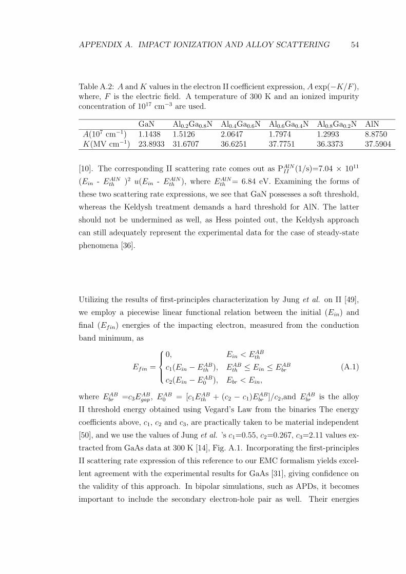
APPENDIX A. IMPACT IONIZATION AND ALLOY SCATTERING 54
Table A.2: A and K values in the electron II coefficient expression, A exp(−K/F ),where, F is the electric field. A temperature of 300 K and an ionized impurityconcentration of 1017 cm−3 are used.
GaN Al0.2Ga0.8N Al0.4Ga0.6N Al0.6Ga0.4N Al0.8Ga0.2N AlNA(107 cm−1) 1.1438 1.5126 2.0647 1.7974 1.2993 8.8750K(MV cm−1) 23.8933 31.6707 36.6251 37.7751 36.3373 37.5904
[10]. The corresponding II scattering rate comes out as PAlNII (1/s)=7.04 × 1011
(Ein - EAlNth )2 u(Ein - EAlN
th ), where EAlNth = 6.84 eV. Examining the forms of
these two scattering rate expressions, we see that GaN possesses a soft threshold,
whereas the Keldysh treatment demands a hard threshold for AlN. The latter
should not be undermined as well, as Hess pointed out, the Keldysh approach
can still adequately represent the experimental data for the case of steady-state
phenomena [36].
Utilizing the results of first-principles characterization by Jung et al. on II [49],
we employ a piecewise linear functional relation between the initial (Ein) and
final (Efin) energies of the impacting electron, measured from the conduction
band minimum, as
Efin =
0, Ein < EABth
c1(Ein − EABth ), EAB
th ≤ Ein ≤ EABbr
c2(Ein − EAB0 ), Ebr < Ein,
(A.1)
where EABbr =c3E
ABgap , EAB
0 = [c1EABth + (c2 − c1)E
ABbr ]/c2,and EAB
br is the alloy
II threshold energy obtained using Vegard’s Law from the binaries The energy
coefficients above, c1, c2 and c3, are practically taken to be material independent
[50], and we use the values of Jung et al. ’s c1=0.55, c2=0.267, c3=2.11 values ex-
tracted from GaAs data at 300 K [14], Fig. A.1. Incorporating the first-principles
II scattering rate expression of this reference to our EMC formalism yields excel-
lent agreement with the experimental results for GaAs [31], giving confidence on
the validity of this approach. In bipolar simulations, such as APDs, it becomes
important to include the secondary electron-hole pair as well. Their energies

APPENDIX A. IMPACT IONIZATION AND ALLOY SCATTERING 55
Figure A.1: Electron II coefficient versus inverse electric field. Dotted lines indi-cate the results when alloy scattering is not included, after Jung [49].
and momenta should be assigned in such a way to meet conservation laws as
much as possible; more vital is the momentum conservation for the current gain
considerations.
Returning to the AlxGa1−xN system, electron II coefficient, , for several alloy
compositions are plotted in Fig. A.2 with respect to electric field, F . These results
are obtained for a temperature of 300 K and an ionized impurity concentration of
1017 cm−3. We note that these curves do not obey Wolff’s form, A exp(−K/F 2),
but rather can be faithfully represented using Shockley’s form of A exp(−K/F );
refer to Table A.1 for a listing of these constants, A and K. In this connection,
we find it useful to add Bude and Hess’s remark that the functional dependence
of on F is closely related to the rise of density of states in the most important
energy range, and not as much on the question of whether lucky electrons are
important for the ionization or not [51].
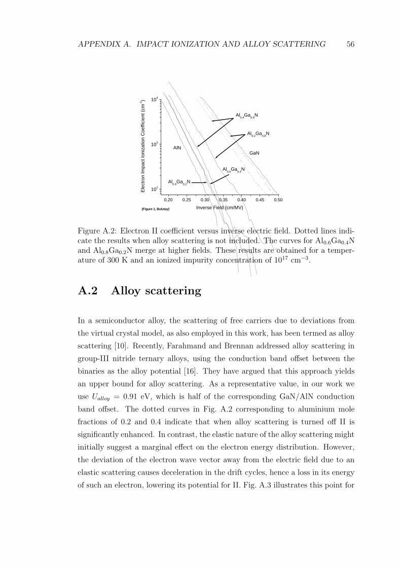
APPENDIX A. IMPACT IONIZATION AND ALLOY SCATTERING 56
0.20 0.25 0.30 0.35 0.40 0.45 0.50
102
103
104
[Figure 1, Bulutay]
Al0.6
Ga0.4
N
Al0.8
Ga0.2
N
Al0.4
Ga0.6
N
Al0.2
Ga0.8
N
AlNGaN
Ele
ctro
n Im
pact
Ioni
zatio
n C
oeffi
cien
t (cm
-1)
Inverse Field (cm/MV)
Figure A.2: Electron II coefficient versus inverse electric field. Dotted lines indi-cate the results when alloy scattering is not included. The curves for Al0.6Ga0.4Nand Al0.8Ga0.2N merge at higher fields. These results are obtained for a temper-ature of 300 K and an ionized impurity concentration of 1017 cm−3.
A.2 Alloy scattering
In a semiconductor alloy, the scattering of free carriers due to deviations from
the virtual crystal model, as also employed in this work, has been termed as alloy
scattering [10]. Recently, Farahmand and Brennan addressed alloy scattering in
group-III nitride ternary alloys, using the conduction band offset between the
binaries as the alloy potential [16]. They have argued that this approach yields
an upper bound for alloy scattering. As a representative value, in our work we
use Ualloy = 0.91 eV, which is half of the corresponding GaN/AlN conduction
band offset. The dotted curves in Fig. A.2 corresponding to aluminium mole
fractions of 0.2 and 0.4 indicate that when alloy scattering is turned off II is
significantly enhanced. In contrast, the elastic nature of the alloy scattering might
initially suggest a marginal effect on the electron energy distribution. However,
the deviation of the electron wave vector away from the electric field due to an
elastic scattering causes deceleration in the drift cycles, hence a loss in its energy
of such an electron, lowering its potential for II. Fig. A.3 illustrates this point for

APPENDIX A. IMPACT IONIZATION AND ALLOY SCATTERING 57
0 2 4 6 8 1010-5
10-4
10-3
[Figure 2, Bulutay]
w/o alloy scattering
Al0.4
Ga0.6
N
F=3.5 MV/cm
Ele
ctro
n E
nerg
y D
istr
ibut
ion
(arb
. uni
ts)
Energy (eV)
Figure A.3: Electron energy distribution for Al0.4Ga0.6N at an electric field of 3.5MV/cm, with (solid) and without (dotted) the alloy scattering. A temperatureof 300 K and an ionized impurity concentration of 1017 cm−3 are considered
Al0.4Ga0.6N (which is an important alloy composition for solar-blind applications)
at an electric field value of 3.5 MV/cm; the depletion of the high energy tail of
the distribution function due to alloy scattering explains the decrease in the II
coefficient obtained in Fig. A.2. However, we would like to draw attention to
two simplifications in our approach inherited from the treatment of Fischetti and
Laux [17]. The alloy scattering is implemented as an intravalley process due to
its small wavelength attenuation [17]; in the case of closely located valleys, like U
and M , this may become rather crude. More importantly, the distribution of the
final scattering angles is assumed to be isotropic, even though at higher energies
alloy scattering attains a forward directional character [52]. Thus, we are lead to
think that the effect of the alloy scattering may still be somewhat overestimated.