Embed Size (px)
Citation preview
1
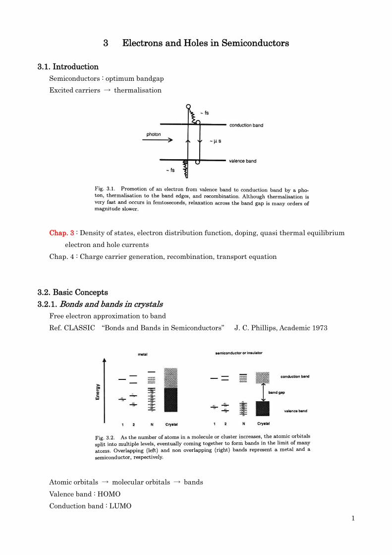
3 Electrons and Holes in Semiconductors
3.1. Introduction
Semiconductors : optimum bandgap
Excited carriers → thermalisation
Chap. 3 : Density of states, electron distribution function, doping, quasi thermal equilibrium
electron and hole currents
Chap. 4 : Charge carrier generation, recombination, transport equation
3.2. Basic Concepts
3.2.1. Bonds and bands in crystals
Free electron approximation to band
Ref. CLASSIC “Bonds and Bands in Semiconductors” J. C. Phillips, Academic 1973
Atomic orbitals → molecular orbitals → bands
Valence band : HOMO
Conduction band : LUMO
2
Semiconductors : eVEg 35.0
Semi-metals : eVEg 5.00
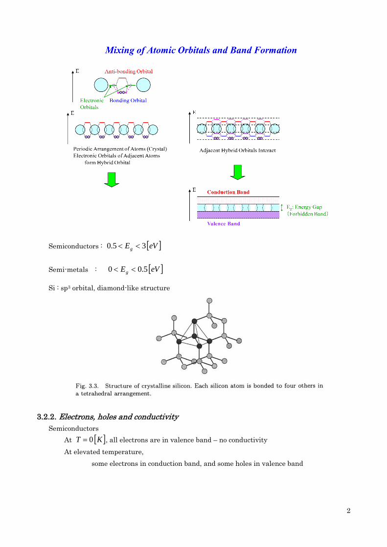
Si : sp3 orbital, diamond-like structure
3.2.2. Electrons, holes and conductivity
Semiconductors
At KT 0 , all electrons are in valence band – no conductivity
At elevated temperature,
some electrons in conduction band, and some holes in valence band
3
3.3. Electron States in Semiconductors
3.3.1. Band structure
Electronic states in crystalline
Solving Schrödinger equation in periodic potential (infinite)
Bloch wavefunction
rk
k rrk i
i eu, (3.1)
for crystal band i and a wavevector k, which is a good quantum number.
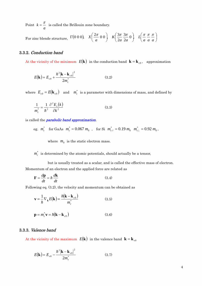
The energy E against wavevector k is called by crystal band structure.
Typical band diagram plotted along the 3 major directions in the reciprocal space.
111,011,001,000 LMX
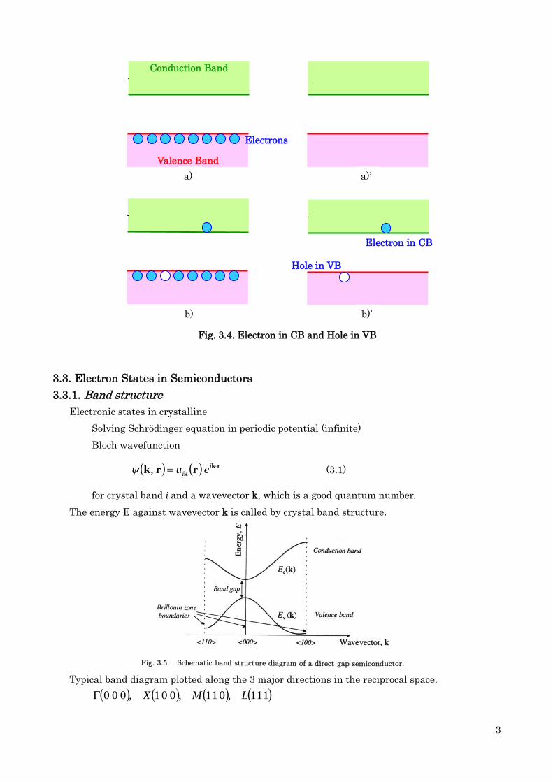
a)
Conduction Band
Valence Band
Electrons
a)’
Electron in CB
b) b)’
Hole in VB
Fig. 3.4. Electron in CB and Hole in VB
4
Point a
k
is called the Brillouin zone boundary.
For zinc blende structure,
aaaL
aaK
aX
,0
2
3
2
3,00
2,000
3.3.2. Conduction band
At the vicinity of the minimum kE in the conduction band 0ckk , approximation
*
2
0
2
02 c
c
cm
EEkk
k
(3.2)
where 00 cc EE k and *
cm is a parameter with dimensions of mass, and defined by
2
2
2*
11
k
kE
m
c
c
(3.3)
is called the parabolic band approximation.
eg. *
cm for GaAs 0
* 067.0 mmc , for Si 0
*
// 19.0 mmc 0
* 92.0 mmc ,
where 0m is the static electron mass.
*
cm is determined by the atomic potentials, should actually be a tensor,
but is usually treated as a scalar, and is called the effective mass of electron.
Momentum of an electron and the applied force are related as
dt
d
dt
d kpF (3.4)
Following eq. (3.2), the velocity and momentum can be obtained as
*
01
c
c
mE
kkkv k
(3.5)
0
*
ccm kkvp (3.6)
3.3.3. Valence band
At the vicinity of the maximum kE in the valence band 0vkk
*
2
0
2
02 v
v
vm
EEkk
k
(3.7)
5
where 00 vv EE k and *
vm is the effective mass of hole.
*
01
v
v
mE
kkkv k
(3.8)
0
*
vvm kkvp (3.9)
2
2
2*
11
k
kE
m
v
v
(3.10)
eg. *
vm for GaAs 0
* 5.0 mmv , for Si 0
* 54.0 mmv ,
*
cm is the curvature of the band.
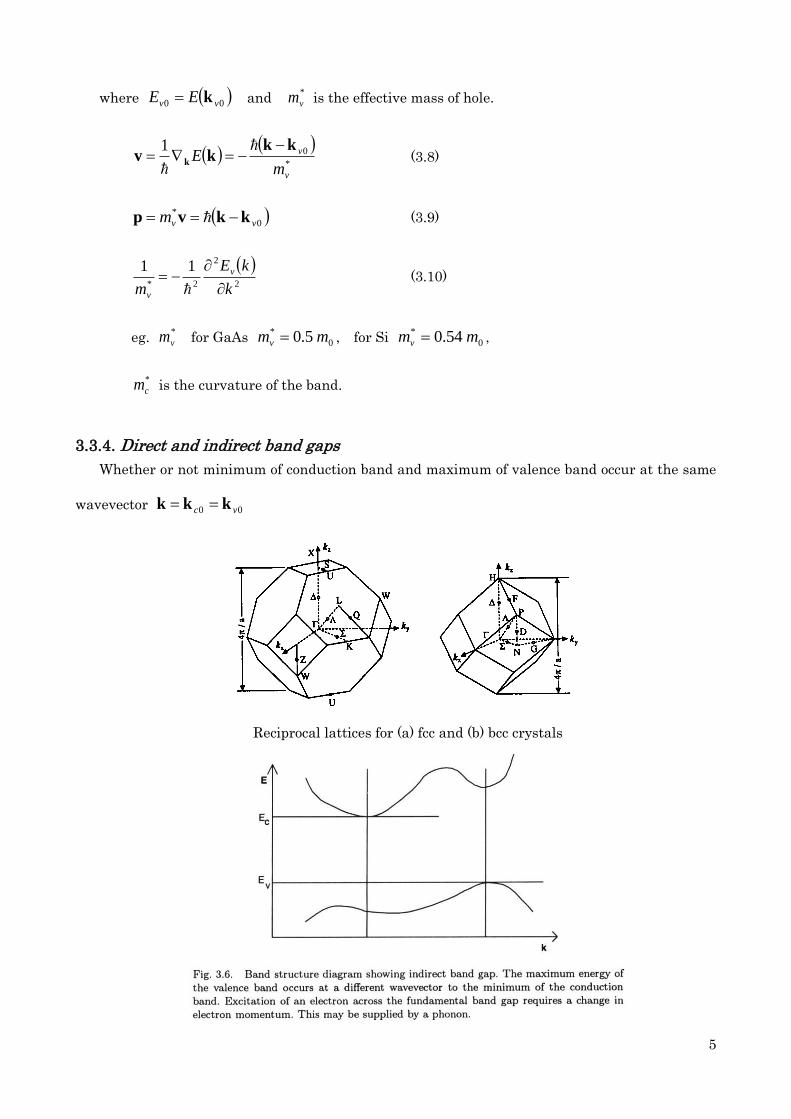
3.3.4. Direct and indirect band gaps
Whether or not minimum of conduction band and maximum of valence band occur at the same
wavevector 00 vc kkk
Reciprocal lattices for (a) fcc and (b) bcc crystals
6
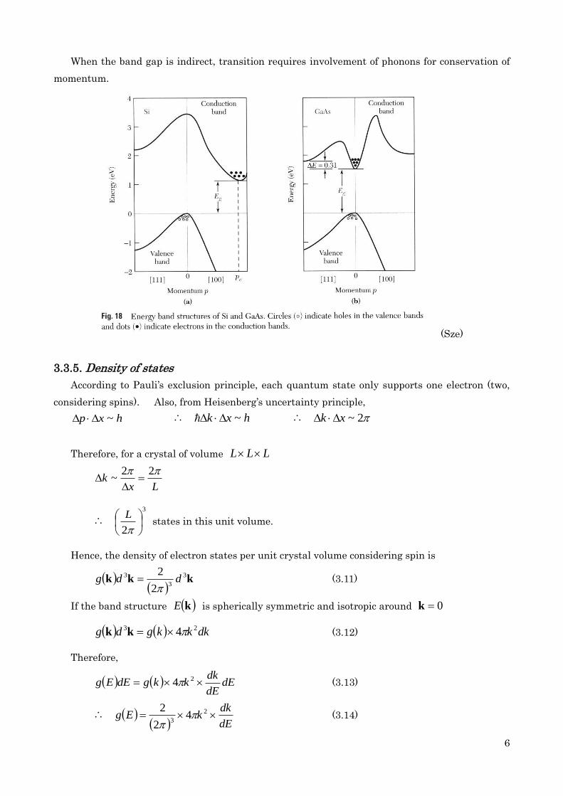
When the band gap is indirect, transition requires involvement of phonons for conservation of
momentum.
(Sze)
3.3.5. Density of states
According to Pauli’s exclusion principle, each quantum state only supports one electron (two,
considering spins). Also, from Heisenberg’s uncertainty principle,
hxp ~ ∴ hxk ~ ∴ 2~xk
Therefore, for a crystal of volume LLL
Lx
k 22
~
∴
3
2
L states in this unit volume.
Hence, the density of electron states per unit crystal volume considering spin is
kkk3
3
3
2
2ddg
(3.11)
If the band structure kE is spherically symmetric and isotropic around 0k
dkkkgdg 23 4kk (3.12)
Therefore,
dEdE
dkkkgdEEg 24 (3.13)
∴ dE
dkkEg 2
34
2
2
(3.14)
7
From eq. (3.2) *
2
0
2
02 c
c
cm
EEkk
k
∴ 02
*
2 2c
c EEm
k
(3.15)
Similarly, for the valence band (hole)
∴ EEm
k vv 02
*
2 2
(3.15’)
Differentiating (3.15)
21
0
21
2
*2c
c EEm
k
∴ 21
0
21
2
*2
2
1
c
c EEm
dE
dk
Therefore, from (3.14)
21
0
23
2
*
2
21
0
23
2
*
3
21
0
21
2
*
02
*
3
21
0
21
2
*
2
3
2
3
2
2
12
2
4
2
2
124
2
2
2
2
14
2
24
2
2
c
c
c
c
cc
cc
cc
c
EEm
EEm
EEm
EEm
EEm
kdE
dkkEg
(3.16)
Similarly,
21
0
23
2
*
2
2
2
1EE
mEg v
vv
(3.17)
Question : Derive the DOS for 2D and 1D materials. (Box 3.3)
Excitons
A bound state of a pair of electron and hole of same k .
The wavefunction can be described as
rkrk ,, heex
Satisfying a hydrogenic effective mass equation
exexex
s
ex Eq
rr
42
22
*
2
* : reduced effective mass of e-h pair
exE : binding energy of the exciton
8
22
2
0
0
*
l
Ryd
mE
s
ex
3.3.6 Electron distribution function
Fermi function in semiconductors
1exp
1
Tk
EEEf
B
F
This can be expressed in terms of rk,f although the energy is only dependent on the
wavevector.
krkkkr 33 , dfgdn
The total electron density is given by
kkrkkr
CBc dfgn 3, (3.20)
k
krkkrVB
v dfgp 3,1 (3.21)
3.3.7 Electron and hole currents
Using the above formalism
k
krkkkrCB
c
c
n dfgm
qJ 3
*,
(3.22)
k
krkkkrVB
v
v
p dfgm
qJ 3
*,1
(3.23)
3.4. Semiconductor in equilibrium
3.4.1. Fermi Dirac statistics
Equilibrium : no net charge exchange. In this case, it is independent of position.
TE,Ef,f F ,0 krk (3.24)
1
1,0
TkEEFBFe
TEE,f (3.25)
3.4.2. Electron and hole densities in equilibrium
The number density of electrons En with energy in the range between E and EE
dETEE,fEgdEEn F ,0 (3.26)
9
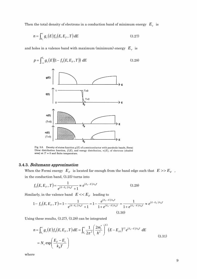
Then the total density of electrons in a conduction band of minimum energy cE is
cE
Fc dETEE,fEgn ,0 (3.27)
and holes in a valence band with maximum (minimum) energy vE is
vE
Fv dETEE,fEgp ,1 0 (3.28)
3.4.3. Boltzmann approximation
When the Fermi energy FE is located far enough from the band edge such that FEE ,
in the conduction band, (3.25) turns into
TkEE
TkEEFBF
BF
ee
TEE,f
1
1,0 (3.29)
Similarly, in the valence band FEE leading to
TkEE
TkEETkEE
TkEE
TkEEFBF
BFBF
BF
BF
eee
e
eTEE,f
1
1
11
1
11,1 0
(3.30)
Using these results, (3.27), (3.28) can be integrated
Tk
EEN
dEeEEm
dETEE,fEgn
B
cFc
E
TkEE
cc
EFc
c
BF
c
exp
2
2
1,
21
0
23
2
*
20
(3.31)
where
10
23
2
*
22
TkmN Bc
c (3.32)
For holes in valence band
vE
B
FvvFv
Tk
EENdETEE,fEgp exp,1 0 (3.33)
where
23
2
*
22
TkmN Bv
v (3.34)
And the product np is given as
TkE
vcBgeNNnp
(3.35)
This is actually a constant and the intrinsic carrier density in suffice the relation
TkE
vciBgeNNnpn
2
(3.36)
Introducing intrinsic potential energy iE , which is the Fermi level for intrinsic semiconductor,
Tk
EEnn
B
iFi exp (3.37)
Tk
EEnp
B
Fi
i exp (3.38)
where
*
*
ln4
3
2
1
ln2
1
2
1
v
cBvc
v
cBvci
m
mTkEE
N
NTkEEE
(3.39)
Electron affinity
Least amount of energy required to remove an electron from solid.
→ Better determined as energy difference between vacuum level and CBM.
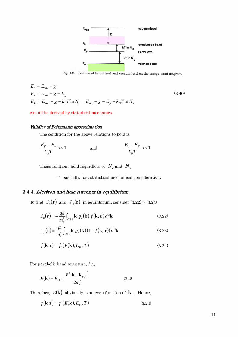
11
vBgvaccBvacF
gvacv
vacc
NTkEENTkEE
EEE
EE
lnln
(3.40)
can all be derived by statistical mechanics.
Validity of Boltzmann approximation
The condition for the above relations to hold is
1
Tk
EE
B
vF and 1
Tk
EE
B
Fc
These relations hold regardless of cN and vN
→ basically, just statistical mechanical consideration.
3.4.4. Electron and hole currents in equilibrium
To find rnJ and rpJ in equilibrium, consider (3.22) ~ (3.24)
k
krkkkrCB
c
c
n dfgm
qJ 3
*,
(3.22)
k
krkkkrVB
v
v
p dfgm
qJ 3
*,1
(3.23)
TE,Ef,f F ,0 krk (3.24)
For parabolic band structure, i.e.,
*
2
0
2
02 c
c
cm
EEkk
k
(3.2)
Therefore, kE obviously is an even function of k . Hence,
TE,Ef,f F ,0 krk (3.24)
12
is also an even function of k and so is
dkkkgdg 23 4kk (3.12)
Consequently,
rkkk ,fgc
is an odd function of k . Therefore, integration of rkkk ,fgc in the entire k -space is 0.
Therefore,
0 rr pn JJ
which means there is no net current in the semiconductor in equilibrium.
3.5. Impurities and Doping
3.5.1. Intrinsic semiconductors
Semiconductors with carrier densities of n (electrons) and p (holes), if the mobilities are n
and p , respectively, the conductivity is given by
pqnq pn (3.41)
In intrinsic semiconductors,
inpn
where in is a small value at room temperature or lower.
Both intrinsic carrier density and conductivity are determined as mere function of temperature
Bandgap, location of Fermi level
At 300K for Si eVEg 12.1 , 3101002.1 cmni , 1161016.3 cm
In semiconductors, mobility increases as a function of temperature due to carriers thermally
excited across the band gap. (ref. What happens with metals?)
At 300K,
Ge : eVEg 74.0 ( eV66.0 ?), 112101.2 cm
13
GaAs : eVEg 42.1 , 1191038.2 cm
(From “Data in Science and Technology, Semiconductors” Springer 1991)
======================
Q. Estimate in for Ge and GaAs at 300K
A. Ge : 3131033.2 cmni GaAs : 36101.2 cmni
======================
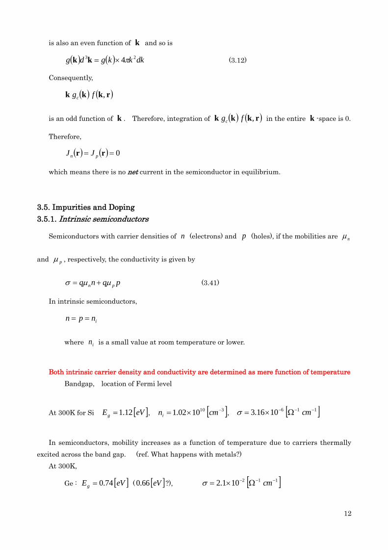
3.5.2. n-type doping
Electrons as majority carrier : By replacing the atoms by those that would readily ionize to
provide free electron (leaving a positive ion). Such atoms are called donor atoms.
In case of Si, this can be accomplished by replacing some of the Si atoms by As, for example.
Typically, this substitution is done on the order of ppm or less.
(Sze)
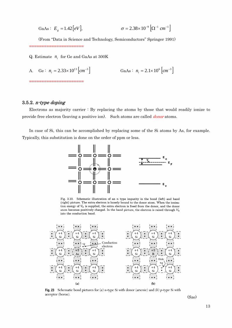
14
Ionisation energy approximated by hydrogenic bond is
Rydm
mV
s
cn 2
0
2
0
*
s : dielectric function of the semiconductor (typically around 10)
Ryd : 13.6 [eV]
∴ eVRydVn 136.0100
1 or smaller
Therefore, room temperature is sufficient to ionise these atoms.
This is depicted in the right hand panel of Fig.3.10.
(Sze)
The density of carriers can be controlled by
1) density of dopants dN
2) donor level (choice of dopants)
3) temperature
Regarding 1), if id nN and the donors are fully ionised at room temperature, then
dNn (3.42)
and
15
d
i
N
np
2
(3.43)
since
TkE
vciBgeNNnpn
2
(3.36)
at equilibrium. Here, obviously,
pn
Hence, electrons are the majority carriers and holes the minority carriers.
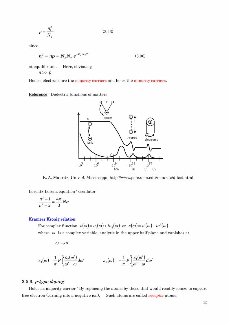
Reference : Dielectric functions of matters
K. A. Mauritz, Univ. S. Mississippi, http://www.psrc.usm.edu/mauritz/dilect.html
Lorentz-Lorenz equation : oscillator
N
n
n
3
4
2
12
2
Kramers-Kronig relation
For complex function 21 i or i
where is a complex variable, analytic in the upper half plane and vanishes at
dP 2
1
1
dP 1
2
1
3.5.3. p-type doping
Holes as majority carrier : By replacing the atoms by those that would readily ionize to capture
free electron (turning into a negative ion). Such atoms are called acceptor atoms.
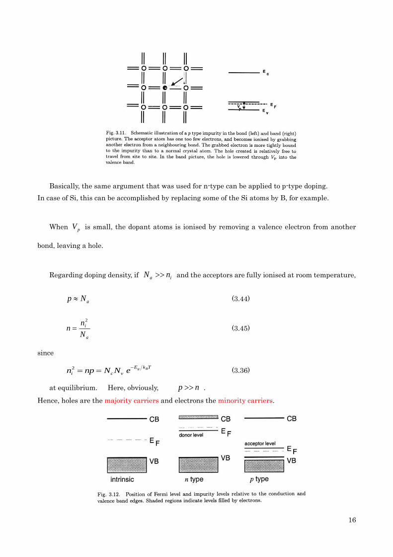
16
Basically, the same argument that was used for n-type can be applied to p-type doping.
In case of Si, this can be accomplished by replacing some of the Si atoms by B, for example.
When pV is small, the dopant atoms is ionised by removing a valence electron from another
bond, leaving a hole.
Regarding doping density, if ia nN and the acceptors are fully ionised at room temperature,
aNp (3.44)
a
i
N
nn
2
(3.45)
since
TkE
vciBgeNNnpn
2
(3.36)
at equilibrium. Here, obviously, np .
Hence, holes are the majority carriers and electrons the minority carriers.
17
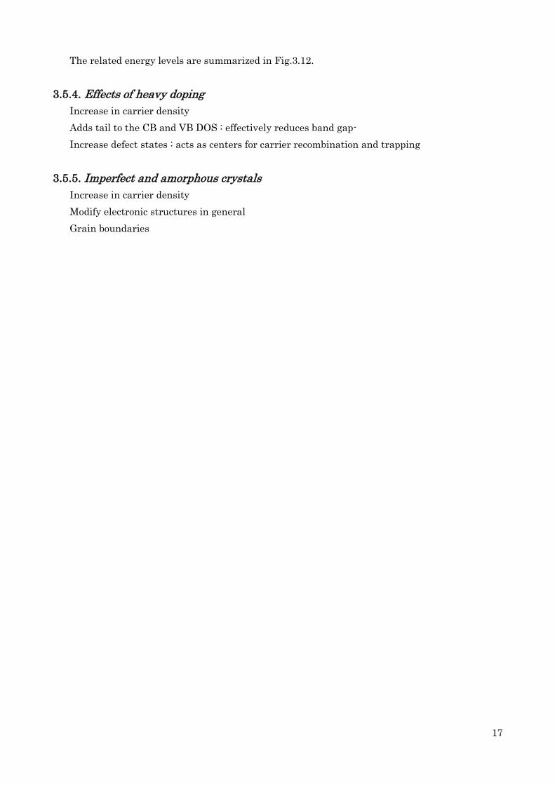
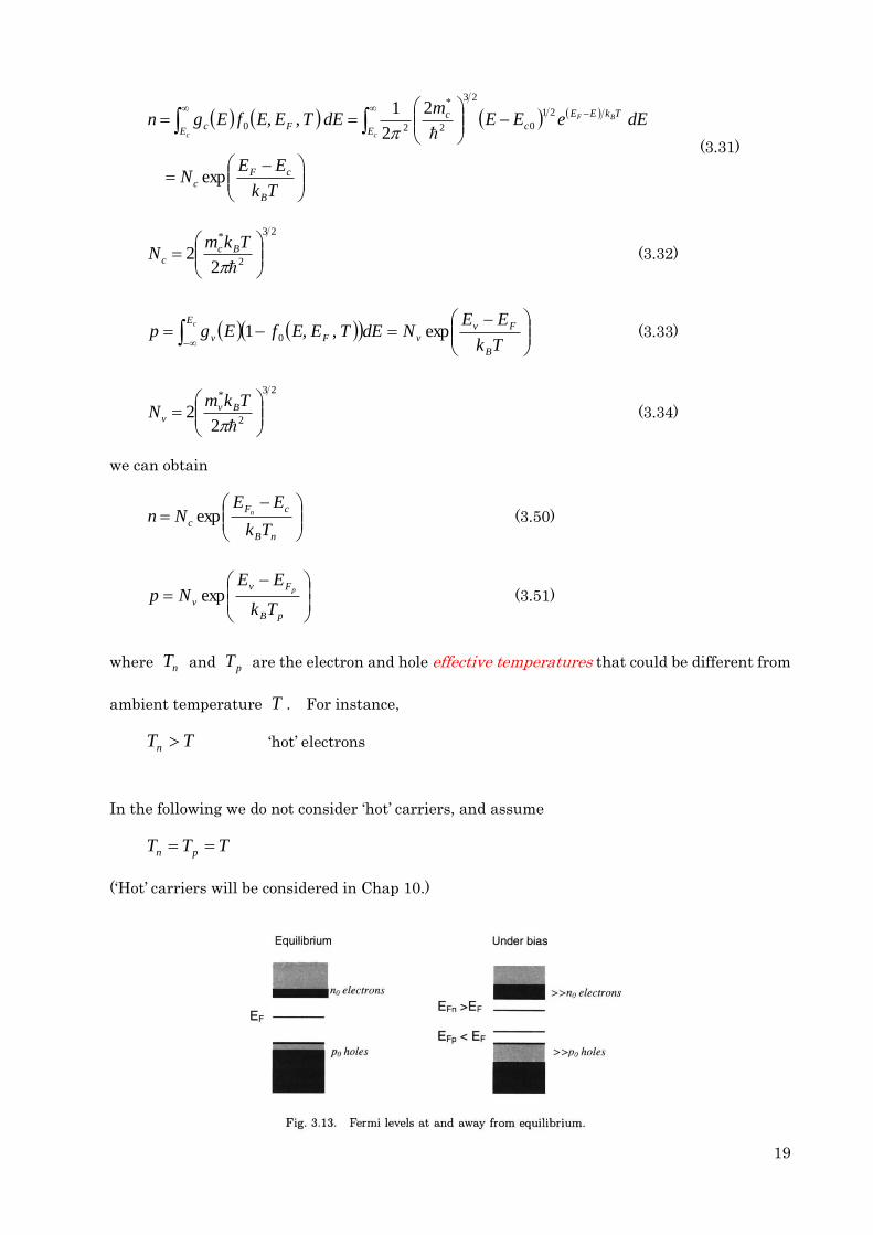
The related energy levels are summarized in Fig.3.12.
3.5.4. Effects of heavy doping
Increase in carrier density
Adds tail to the CB and VB DOS : effectively reduces band gap-
Increase defect states : acts as centers for carrier recombination and trapping
3.5.5. Imperfect and amorphous crystals
Increase in carrier density
Modify electronic structures in general
Grain boundaries
18
3.6. Semiconductor under Bias
Actual devices under operation : non-equilibrium condition
3.6.1. Quasi thermal equilibrium
System disturbed from equilibrium
In quasi thermal equilibrium, for electrons and holes,
nFc TEE,ffn,, 0rk : for electrons
pFv TEE,ffp,, 0rk : for holes
nF TEE,fn,0 and pF TEE,f
p,0 are those of equilibrium, implying there is no net current.
rk,cf and rk,vf are general distribution functions, both r and k dependent.
The Fermi levels defined for this quasi thermal equilibrium is different from those at
equilibrium (and also)
nFE : electron quasi Fermi level
pFE : hole quasi Fermi level
Small correction factor introduced
rkrk ,,, 0 AnFc fTEE,ffn
(3.46)
nBnF
nBnFn
TkEE
TkEEnF ee
TEE,f
1
1,0 (3.47)
rk,Af is the part that is antisymmetric in k .
3.6.2. Electron and hole density under bias
In 3.4.3, relations
Tk
EEnn
B
iFi exp (3.37)
Tk
EEnp
B
Fi
i exp (3.38)
were introduced. These can be applied for the quasi Fermi levels
Tk
EEnn
B
iF
inexp (3.48)
Tk
EEnp
B
Fi
i
p
exp (3.49)
Also applying the results
19
Tk
EEN
dEeEEm
dETEE,fEgn
B
cFc
E
TkEE
cc
EFc
c
BF
c
exp
2
2
1,
21
0
23
2
*
20
(3.31)
23
2
*
22
TkmN Bc
c (3.32)
cE
B
Fv
vFvTk
EENdETEE,fEgp exp,1 0 (3.33)
23
2
*
22
TkmN Bv
v (3.34)
we can obtain
nB
cF
cTk
EENn nexp (3.50)
pB
Fv
vTk
EENp
p
exp (3.51)
where nT and pT are the electron and hole effective temperatures that could be different from
ambient temperature T . For instance,
TTn ‘hot’ electrons
In the following we do not consider ‘hot’ carriers, and assume
TTT pn
(‘Hot’ carriers will be considered in Chap 10.)
20
One thing to be noted for semiconductor under bias is that the Fermi levels for electrons and
holes are NOT identical, i.e.,
FFF EEEpn
and the Fermi levels are split. The difference between the quasi Fermi levels
pn FF EE (3.52)
The relationship between carrier densities was defined by
TkE
vciBgeNNnpn
2
(3.36)
Substituting (3.50) and (3.51) into (3.36)
Tk
i
TkEETkE
vc
TkEEE
vc
pB
Fv
v
nB
cF
c
BBpFnFBg
BpFnFgpn
eneeNN
eNNTk
EEN
Tk
EENnp
2
expexp (3.53)
In general, these quasi Fermi levels nFE and
pFE are not constant throughout the device and
are functions of position.
We consider local quasi equilibrium at any point in the semiconductor, and local quasi
Fermi levels.
3.6.3. Current densities under bias
If the distribution function is symmetric as discussed previously, there would be no current.
Hence, for currents rnJ and rpJ to be non-zero, the distribution function f needs to be
antisymmetric.
----------Box 3.4 Boltzmann Transport eq. and relaxation time approximation ------------------
Let the antisymmetric part of the distribution function f be Af .
Since cf is a function of tandrk, , by definition
t
ff
dt
df
dt
d
dt
df ccc
c
kr
kr (3.54)
where
dt
drv (3.55)
dt
dkF (3.56)
21
Define rk,E as the energy with respect to the conduction band minimum (CBM)
rk,EEE c (3.57)
where
rkrk ,,, 0 AnFc fTEE,ffn
(3.46)
We assume that
nFc TEE,ffn,, 0rk
From (3.47)
TkEETkE
TkEEETkEEFcF
BnFcB
BnFcBnFnn
ee
eeTE,EEfTEE,f
rk
rkrk
,
,00
1
1
1
1,,,
From physical consideration, we can assume that rk,E varies as a function of k , but not
much as function of r .
Therefore, for calculating cfr , let
TkEE
nFc
BnFc
neTEE,ff
,, 0rk
∴
n
nBnFcBnFc
Fc
BB
FcTkEETkEE
c EETk
f
Tk
EEeef
rrrr
0 (3.58)
For calculating cfk , note that nFc EE is a function of r but not of k , and that rk,E
varies as a function of k , but not much as function of r Hence, let rk,E be a function of k ,
but not r . Therefore, using,
TkEETkE
nFc
BnFcB
neeTEE,ff
rkrk
,
0 ,,
rk
rkkk
rk
rk
k
rk
kk
,, 0,
,,
ETk
f
Tk
Eee
eeeef
BB
TkETkEE
TkETkEETkEETkE
c
BBnFc
BBnFcBnFcB
From (3.5)
*
01
c
c
mE
kkkv k
Here, we can assume 00 ck (the result will be the same even if this is not the case).
Hence,
22
vrkkkTk
fE
Tk
ff
BB
c
00 ,
(3.59)
Substituting (3.58) and (3.59) into (3.54) together with dt
d
dt
d kpF (3.4)
t
fEE
Tk
f
t
f
dt
dEE
Tk
f
t
f
Tk
f
dt
dEE
Tk
f
dt
d
t
ff
dt
dkf
dt
d
dt
df
c
Fc
B
c
Fc
B
c
B
Fc
B
c
cc
c
nn
n
vFvvk
v
vkrr
rr
rkr
00
00
(3.60)’
Here, from physical consideration,
Fr cE (gradient of conduction band is the force on the electron)
∴ t
fE
Tk
f
dt
df cF
B
c
n
rv0 (3.60)
To solve this for cf , the following assumptions are made.
1) Intraband relaxation is much more frequent than interband
Intraband relaxation is dominantly phonon scattering with lattice and fast.
collisions
cc
t
f
t
f
2) The distribution relaxes exponentially towards the quasi equilibrium with time
constant
0ff
t
f c
collisions
c
(3.61)
This is called the relaxation time approximation.
Substituting (3.61) into (3.60),
00 ff
ETk
f
dt
df cF
B
c
n
rv
Under steady state, this equals 0,
00 ffE
Tk
f c
F
Bn
rv
nF
B
c ETk
ff rv
10 (3.62)
Therefore,
nF
B
A ETk
ff rv
0 (3.63)
23
(The sign might be wrong, but never mind : it is how the direction is considered)
Substituting for cf , the equation for current becomes
kr
k
r
k
r
kr
k
k
kk
k
kk
kkkvkk
kvkkkrkkk
krkkkr
CBc
c
B
F
CBc
c
cB
F
CBc
cB
F
CBF
B
c
cCB
Ac
c
CBc
c
n
dm
fgTk
qE
dm
fgm
q
Tk
Edfg
m
q
Tk
E
dETk
fgm
qdfg
m
q
dfgm
qJ
n
nn
n
3
2
*0
3
*0*
3
0*
3
0*
3
*
3
*
,
,
(3.64)
Since the term in brackets is NOT a function of bias, we rewrite this as nn where
n is the electron mobility
Then,
nFnn EnJ rr (3.65)
Similarly
pFpp EpJ rr (3.66)
-------------------------END of Box 3.4--------------------------------------------------------
The net current is given by
pn FpFnpn EpEnJJJ rrrrr (3.67)
3.7. Drift and Diffusion
3.7.1. Current equations in terms of drift and difusion
Tk
EENn
B
cFc exp (3.31)
By differentiating both sides
24
cF
B
c
B
cF
c
cB
cF
B
cF
cc
c
B
cF
cc
B
cF
B
cF
c
EETk
nNn
Tk
EEnN
N
n
Tk
EE
Tk
EENN
N
n
Tk
EENN
Tk
EE
Tk
EENn
n
nnn
nnn
rr
rrrr
rrrr
ln
exp
expexpexp
∴ cF
B
c EETk
nNnn
n rrr ln
∴ cBB
cB
cF NTknn
TkNnn
n
TkEE
nlnln rrrrr
∴ nn
TkNTkEE B
cBcFn rrrr ln (3.68)
Similarly, from (3.33)
pp
TkNTkEE B
vBvFp rrrr ln (3.69)
Note the relation (refer to Sze Fig. 4-32, below)
vBgvaccBvacF
gvacv
vacc
NTkEENTkEE
EEE
EE
lnln
(3.40)
The gradient in the conduction/valence band edge is
rr F qEc (3.70)
although, typically 0r .
Similarly
gv EqE rrr F (3.71)
although, typically 0r gE .
25
(Sze)
The electrostatic field is defined by
vacEq
rF 1
(3.72)
Substituting (3.68), (3.70) into (3.65), (3.66)
nFnn EnJ rr (3.65)
nn
TkNTkEE B
cBcFn rrrr ln (3.68)
rr F qEc (3.70)
26
∴
cBnn
BncBn
BcBn
BcBcnn
NTkqnnqD
nTkNTkqn
nn
TkNTkqn
nn
TkNTkEnJ
ln
ln
ln
ln
rrr
rrr
rrr
rrr
F
F
F
r
(3.73)
where
q
TkD B
nn (3.77)’
Similarly
vBgppp NTkEqppqDJ lnrrrr Fr (3.74)
where
q
TkD B
pp (3.77)”
As mentioned, typically 0r , 0r gE , and cN , vN (doping levels) are invariant.
Therefore,
nqnqDJ nnn Fr r (3.75)
pqpqDJ ppp Fr r (3.76)
The first terms are the diffusion current, and the second the drift.
Driving forces
Drift : potential gradient
Diffusion : concentration gradient
27
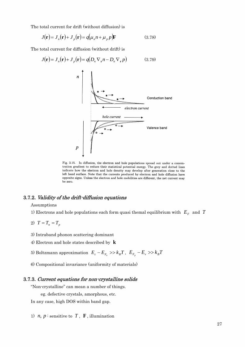
The total current for drift (without diffusion) is
Frrr pnqJJJ pnpn (3.78)
The total current for diffusion (without drift) is
pDnDqJJJ nnpn rrrrr (3.79)
3.7.2. Validity of the drift-diffusion equations
Assumptions
1) Electrons and hole populations each form quasi themal equilibrium with FE and T
2) pn TTT
3) Intraband phonon scattering dominant
4) Electron and hole states described by k
5) Boltzmann approximation TkEE BFc n , TkEE BvFp
6) Compositional invariance (uniformity of materials)
3.7.3. Current equations for non-crystalline solids
“Non-crystalline” can mean a number of things.
eg. defective crystals, amorphous, etc.
In any case, high DOS within band gap.
1) pn, : sensitive to T , F , illumination
28
2) pn , : T , F , pn, dependent
3) conduction due to localized states between band gap
istateslocalized
ipn JJJJ (3.80)
i
iii
istateslocalized
i EgEfEJ (3.81)
i
iii
istateslocalized
i EgEfEJ
iE : mobility of carrier through localized states → mechanism dependent
iEf : (Fermi-Dirac) distribution function
iEg : DOS of localized states
Discussed in Chap 8.
3.8. Summary
Conduction band electrons : nearly free particles responsible for transport
Valence band holes
Equilibrium and Fermi level determining occupancy probability
Doping
Quasi Fermi levels


![Electrons and Holes in Semiconductors - Peoplehu/Chenming-Hu_ch1.pdf · Electrons and Holes in Semiconductors by William Shockley [1], published in 1950, two years after the invention](https://img.dokumen.tips/doc/110x75/5a76a7467f8b9a9c548d7342/electrons-and-holes-in-semiconductors-people-huchenming-huch1pdf-electrons.jpg)


![Hot-Electron Effect in Superconductors and its ...electrons (or holes) in semiconductors (for a review see, e.g., the book of Conwel [1]). The term encompasses electron distributions,](https://img.dokumen.tips/doc/110x75/5f7bf9203d3266082b5ee818/hot-electron-effect-in-superconductors-and-its-electrons-or-holes-in-semiconductors.jpg)