Embed Size (px)
Citation preview
FPGAs�A short introduction
M.BerettaLNF-INFN

EVOLUTION OF INTEGRATED CIRCUITS
EDIT2015–FRASCATIOCTOBER20-29 2M.BERETTA–G.FELICI–P.ALBICOCCO
u 1948: invention of transistors (Bell Labs)
u 1958: Invention of Integrated Circuitsu The idea of making a whole circuit-transistors, wires, and everything else-was
invented by Jack Kilby at Texas Instruments and Robert Noyce at Fairchild Semiconductor almost at the same time
u 1965: Moore’s Law
u In 1965, Gordon Moore at Intel made a prediction that semiconductor technology will double its effectiveness every 18 months
1-2
The evolution of Integrated Circuits
� 1948: Invention of transistor (Bell Labs)
� 1958: Invention of Integrated Circuits
— The idea of making a whole circuit-transistors, wires, and everything else-wasinvented by Jack Kilby at Texas Instruments and Robert Noyce at Fairchild Semiconductor almost at the same time.
� 1965: Moore’s Law
— In 1965, Gordon Moore at Intel made a prediction that semiconductor technologywill double its effectiveness every 18 months
Source Bell Labs
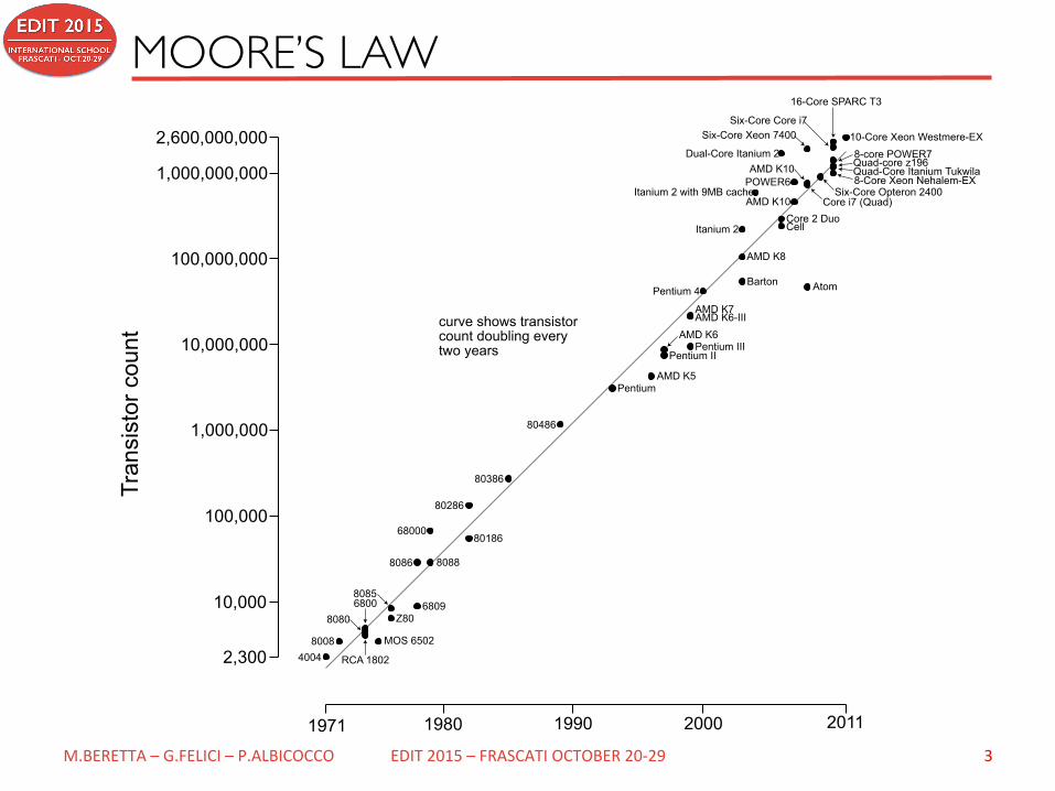
MOORE’S LAW
EDIT2015–FRASCATIOCTOBER20-29 3M.BERETTA–G.FELICI–P.ALBICOCCO
curve shows transistorcount doubling everytwo years
2,300
10,000
100,000
1,000,000
10,000,000
100,000,000
1,000,000,000
2,600,000,000
1971 1980 1990 2000 2011
Date of introduction
40048008
8080
RCA 1802
8085
8088
Z80
MOS 6502
6809
8086
80186
6800
68000
80286
80386
80486
PentiumAMD K5
Pentium IIPentium III
AMD K6AMD K6-IIIAMD K7
Pentium 4Barton Atom
AMD K8
Itanium 2 CellCore 2 Duo
AMD K10Itanium 2 with 9MB cache
POWER6
Core i7 (Quad)Six-Core Opteron 2400
8-Core Xeon Nehalem-EXQuad-Core Itanium TukwilaQuad-core z1968-core POWER7
10-Core Xeon Westmere-EX
16-Core SPARC T3
Six-Core Core i7Six-Core Xeon 7400
Dual-Core Itanium 2AMD K10
Microprocessor Transistor Counts 1971-2011 & Moore's Law
Tran
sist
or c
ount

MICROPROCESSORS CLOCK FREQUENCIES
EDIT2015–FRASCATIOCTOBER20-29 4M.BERETTA–G.FELICI–P.ALBICOCCO

CLASSIFICATION OF INTEGRATED CIRCUITS
EDIT2015–FRASCATIOCTOBER20-29 5M.BERETTA–G.FELICI–P.ALBICOCCO
u Microprocessors
u Memory chips (SRAM, DRAM, Flash, ROM, PROM)
u Standard Components (74LS..)
u Application-Specific Integrated Circuitsu Widely used in communication, network, and multimedia systemsu For a given application, ASIC solutions are normally more effective than the
solutions based on running software on microprocessorsu Many chips in cellular phones, network routers, and game consoles are ASICsu Most SoC (Systems-on-a-Chip) chips are ASICsu Programmable devices (PLA/PAL-CPLD-FPGA)

ASIC DESIGN METHODOLOGIES
EDIT2015–FRASCATIOCTOBER20-29 6M.BERETTA–G.FELICI–P.ALBICOCCO
ASIC DESIGN FPGA DESIGN

FULL-CUSTOM DESIGN METHODOLOGY
EDIT2015–FRASCATIOCTOBER20-29 7M.BERETTA–G.FELICI–P.ALBICOCCO
1-7
Full-Custom Design Methodology
Function Partition
Schematic Design
Function And Timing verification
Pass
Fail
Including transistor sizing
Layout DesignIncluding placement & routing
Post-Layoutsimulation
Pass
Fail
Go to fabrication
ASIC Chips
¾ It is a time consuming manual process, not pre-developed libraries needed.IT IS A TIME CONSUMING MANUAL PROCESS. NO PRE-DEVELOPED LIBRARY ARE REQUIREDPros: complete flexibility, high degree of optimization in performance, power consumption and application areaCons: large amount of design effort, expensive, time to market

STANDARD-CELL BASED DESIGN METHODOLOGY
EDIT2015–FRASCATIOCTOBER20-29 8M.BERETTA–G.FELICI–P.ALBICOCCO
1-9
Standard-Cell Based Design Methodology
High-level (RTL or behavioral-level) design VHDL or Verilog coding
High-level verification VHDL or Verilog simulation
Logic synthesis Logic gate library
Gate-level verification
Placement & Routing Cell layout library
Post-Layout verification Go to fabrication
Fail
Pass
Pass
Fail
Fail Pass
¾ It is highly automated, but need pre-developed libraries.ITISHIGHLYAUTOMATED.NEEDPRE-DEVELOPEDLIBRARIESPros:savedesignNmeandmoney.Reduceriskcomparedtoafull-customdesignCons:sNllincurshighnon-recurring-engineering(NRE)costandlongmanufactureNme
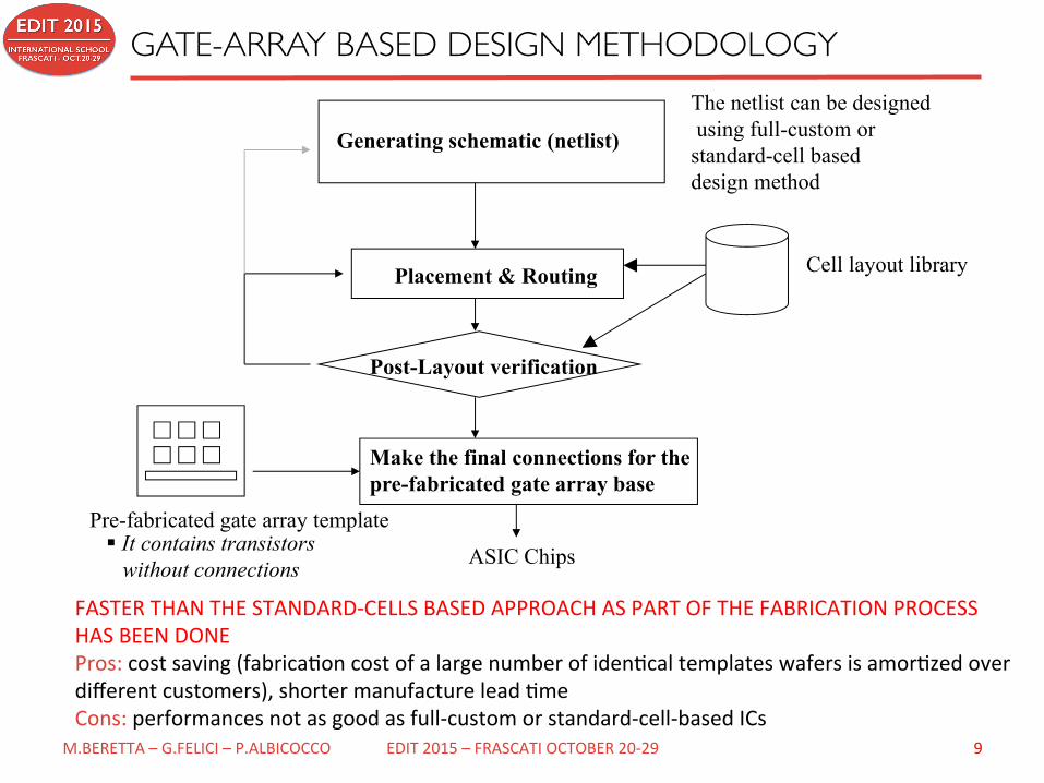
GATE-ARRAY BASED DESIGN METHODOLOGY
EDIT2015–FRASCATIOCTOBER20-29 9M.BERETTA–G.FELICI–P.ALBICOCCO
FASTERTHANTHESTANDARD-CELLSBASEDAPPROACHASPARTOFTHEFABRICATIONPROCESSHASBEENDONEPros:costsaving(fabricaNoncostofalargenumberofidenNcaltemplateswafersisamorNzedoverdifferentcustomers),shortermanufactureleadNmeCons:performancesnotasgoodasfull-customorstandard-cell-basedICs
1-11
Gate-Array Based Design Methodology
Generating schematic (netlist)
The netlist can be designedusing full-custom or
standard-cell based design method
Placement & Routing Cell layout library
Post-Layout verification
Pre-fabricated gate array template
Make the final connections for thepre-fabricated gate array base
ASIC Chips� It contains transistors without connections
¾ This approach is faster than the standard-cell based approach because part ofthe fabrication process has been complete.

FPGA BASED DESIGN METHODOLOGY
EDIT2015–FRASCATIOCTOBER20-29 10M.BERETTA–G.FELICI–P.ALBICOCCO
1-13
FPGA Based Design Methodology
Schematic Capture
HDL coding &Logic Synthesis
netlist
ImplementationTechnology mappingPlacement & routing
FPGA celllibrary
Verification Timing verification
Pass
Fail
Generate FPGA Bit StreamDownload
FPGA
¾ This approach has extremely fast turn-out time since FPGA devices has been fabricated.THISAPPRACHHASEXTREMELYFASTTURN-OUTTIMESINCETHEFPGADEVICESHASBEEN
ALREADYFABRICATED

COMPARISON OF DESIGN METODOLOGIES
EDIT2015–FRASCATIOCTOBER20-29 11M.BERETTA–G.FELICI–P.ALBICOCCO
1-14
Comparison of Design Methodologies
Full-custom design
Standard-cellbased design
Gate-arraybased design
FPGA-based design
Speed +++ ++ + -
Integration density +++ ++ + --
High-volume device cost ++ ++ + +
low-volume device cost --- -- + +++
Custom mask layer All All Some None
Fabrication time --- -- - +++
Time to Market --- -- ++ +++
Risk reduction --- -- - +++
Future design modification --- -- - +++
+ desirable; - not desirable 1-14
Comparison of Design Methodologies
Full-custom design
Standard-cellbased design
Gate-arraybased design
FPGA-based design
Speed +++ ++ + -
Integration density +++ ++ + --
High-volume device cost ++ ++ + +
low-volume device cost --- -- + +++
Custom mask layer All All Some None
Fabrication time --- -- - +++
Time to Market --- -- ++ +++
Risk reduction --- -- - +++
Future design modification --- -- - +++
+ desirable; - not desirable

FPGA ADVANTAGES AND APPLICATIONS
EDIT2015–FRASCATIOCTOBER20-29 12M.BERETTA–G.FELICI–P.ALBICOCCO
u FPGAsPros: Fast turn-out time, re-programming capability, dynamic reconfiguration capabilityCons: performances and integration are not as good as full-custom or standard-cell-based ICs, power consumption
NB: integration issue mitigated by SoC technology (microprocessors + FPGA in the same device)
u FPGA APPLICATIONSu Ideal platform for prototypingu Providing fast implementation to reduce time-to-marketu Cost effective solutions for products with small volumes on demandu Implementing hardware systems requiring re-programming flexibilityu Implementing dynamically re-configurable systems

FPGA MARKET
EDIT2015–FRASCATIOCTOBER20-29 13M.BERETTA–G.FELICI–P.ALBICOCCO
© Copyright 2012 Xilinx
Xilinx 47%
Altera 41%
Others 12%
PLD Market Segment Share Calendar Year 2011
Page 7
With 47% Market Share, Xilinx is the Industry’s #1 PLD Supplier
Source: iSuppli

FPGAs AND MOORE’S LAW
EDIT2015–FRASCATIOCTOBER20-29 14M.BERETTA–G.FELICI–P.ALBICOCCO
Copyright Xilinx 2014.
FPGAs and Moore’s Law
10,000x More Logic– Plus Embedded IP
• Memory• Microprocessor• DSP• Gigabit Serial I/O
100x Faster5000x Lower Power 10,000x Lower Cost
Ages 3

TYPICAL FPGA ARCHITECTURE - 1
EDIT2015–FRASCATIOCTOBER20-29 15M.BERETTA–G.FELICI–P.ALBICOCCO
I/O BLOCK
CONFIGURABLE LOGIC BLOCK
HORIZONTAL ROUTING CHANNELS
VERTICAL ROUTING CHANNELS
DIGITAL CLOCK MANAGER
BLOCK RAM

TYPICAL FPGA ARCHITECTURE - 2
EDIT2015–FRASCATIOCTOBER20-29 16M.BERETTA–G.FELICI–P.ALBICOCCO
Basic FPGA architecture

CONFIGURABLE LOGIC BLOCKS (CLBs)
EDIT2015–FRASCATIOCTOBER20-29 17M.BERETTA–G.FELICI–P.ALBICOCCO
u CLB is the basic logic unit in a FPGAu EveryCLBconsistsofaconfigurableswitchmatrixwith4or6inputs,someselecNoncircuitry
(MUX,etc),andflip-flopsu Theswitchmatrixishighlyflexibleandcanbeconfiguredtohandlecombinatoriallogic,shid
registersorRAM
BASICCONFIGURABLELOGICBLOCKSTRUCTURE

CLBs - DETAILS
EDIT2015–FRASCATIOCTOBER20-29 18M.BERETTA–G.FELICI–P.ALBICOCCO
The fig .1 shows the general structure of FPGA chip. It consists of a large number of programmable logic blocks surrounded by programmable I/O block. The programmable logic blocks of FPGA are smaller and less capable than a PLD, but an FPGA chip contains a lot more logic blocks to make it more capable. As shown in fig.1 the logic blocks are distributed across the entire chip. These logic blocks can be interconnected with programmable inter connections.
Xilinx, Inc inverted FPGAs, and in this section we will see the FPGA
architecture used by Xilinx. The programmable logic blocks inn the Xilinx family of FPGAs are called Configurable Logic Blocks (CLBs).The Xilinx architecture uses, CLBs, I/O blocks switch matrix and an external memory chip to realize a logic function. It uses external memory to store the interconnection information. Therefore, the device can be reprogrammed by simply changing the configuration data stored in the memory.
Configurable Logic Block:
u CLBs contain RAM memory cellsu CLBs can be configured to realize any
function of 5 or 4 variablesu Functions are stored in the true table formu Trapezoidal blocks represent multiplexeru Multiplexer can be programmed to
implement to select one input
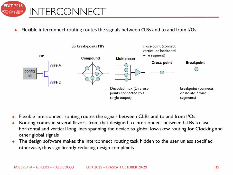
INTERCONNECT
EDIT2015–FRASCATIOCTOBER20-29 19M.BERETTA–G.FELICI–P.ALBICOCCO
u Flexible interconnect routing routes the signals between CLBs and to and from I/Osu Routing comes in several flavors, from that designed to interconnect between CLBs to fast
horizontal and vertical long lines spanning the device to global low-skew routing for Clocking and other global signals
u The design software makes the interconnect routing task hidden to the user unless specified otherwise, thus significantly reducing design complexity
u FlexibleinterconnectrouNngroutesthesignalsbetweenCLBsandtoandfromI/Os
cross-point (connect vertical or horizontal wire segment)
breakpoint (connects or isolate 2 wire segments)
Decoded mux (2n cross-points connected to a single output)
Six break-points PIPs

SELECTIO (IOBs)
EDIT2015–FRASCATIOCTOBER20-29 20M.BERETTA–G.FELICI–P.ALBICOCCO
u Today’s FPGAs provide support for dozens of I/O standards thus providing the ideal interface bridge in your system
u I/O in FPGAs is grouped in banks with each bank independently able to support different I/O standards
u Today’s leading FPGAs provide over a dozen I/O banks, thus allowing flexibility in I/O support.
BASICSELECTIO(IOBs)STRUCTURE

MEMORY AND CLOCK MANAGEMENT
EDIT2015–FRASCATIOCTOBER20-29 21M.BERETTA–G.FELICI–P.ALBICOCCO
u MEMORYu EmbeddedBlockRAMmemoryisavailableinmostFPGAs,whichallowsforon-chipmemory
inyourdesign.u XilinxFPGAsprovideupto10Mbitsofon-chipmemoryin36kbitblocksthatcansupporttrue
dual-portoperaNon
u COMPLETECLOCKMANAGEMENTu DigitalclockmanagementisprovidedbymostFPGAsintheindustry(allXilinxFPGAshave
thisfeature).u ThemostadvancedFPGAsfromXilinxofferbothdigitalclockmanagementandphase-looped
lockingthatprovideprecisionclocksynthesiscombinedwithjiherreducNonandfiltering.

XC2064 - THE FIRST FPGA (1985)
EDIT2015–FRASCATIOCTOBER20-29 22M.BERETTA–G.FELICI–P.ALBICOCCO
Copyright Xilinx 2014.
64 flip flops128 3-LUTs58 I/O pins18MHz (toggle)
2um 2LM
Ages 6
XC2064 The First FPGA (1985)

2015 - XILINX FPGAs
EDIT2015–FRASCATIOCTOBER20-29 23M.BERETTA–G.FELICI–P.ALBICOCCO
Memory
Embedded Block RAM memory is available in most FPGAs, which allows for on-chip memory in your design. Theseallow for on-chip memory for your design. Xilinx FPGAs provide up to 10Mbits of on-chip memory in 36kbit blocksthat can support true dual-port operation.
Complete Clock Management
Digital clock management is provided by most FPGAs in the industry (all Xilinx FPGAs have this feature). The mostadvanced FPGAs from Xilinx offer both digital clock management and phase-looped locking that provide precisionclock synthesis combined with jitter reduction and filtering.
>>Learn more about FPGA Features and Design
Xilinx FPGAsXilinx offers the broadest lineup of FPGAs providing advance features, low-power, high-performance, and high value for any FPGAdesign. Below is an overview of Xilinx leading FPGA families.
Features Artix™-7 Kintex™-7 Virtex®-7 Spartan®-6 Virtex-6
Logic Cells 215,000 480,000 2,000,000 150,000 760,000
BlockRAM 13Mb 34Mb 68Mb 4.8Mb 38Mb
DSP Slices 740 1,920 3,600 180 2,016
DSP Performance(symmetric FIR)
930GMACS 2,845GMACS 5,335GMACS 140GMACS 2,419GMACS
Transceiver Count 16 32 96 8 72
Transceiver Speed 6.6Gb/s 12.5Gb/s 28.05Gb/s 3.2Gb/s 11.18Gb/s
Total Transceiver Bandwidth(full duplex)
211Gb/s 800Gb/s 2,784Gb/s 50Gb/s 536Gb/s
Memory Interface (DDR3) 1,066Mb/s 1,866Mb/s 1,866Mb/s 800Mb/s 1,066Mb/s
PCI Express® Interface x4 Gen2 Gen2x8 Gen3x8 Gen1x1 Gen2x8
Analog Mixed Signal(AMS)/XADC
Yes Yes Yes - Yes
Configuration AES Yes Yes Yes Yes Yes
I/O Pins 500 500 1,200 576 1,200
I/O Voltage 1.2V, 1.35V, 1.5V, 1.8V,2.5V, 3.3V
1.2V, 1.35V, 1.5V, 1.8V,2.5V, 3.3V
1.2V, 1.35V, 1.5V, 1.8V,2.5V, 3.3V
1.2V, 1.5V, 1.8V,2.5V, 3.3V
1.2V, 1.5V,1.8V, 2.5V
EasyPath™ Cost ReductionSolution
- Yes Yes - Yes
>>View all FPGAs from Xilinx
FPGA ApplicationsDue to their programmable nature, FPGAs are an ideal fit for many different markets. As the industry leader, Xilinx providescomprehensive solutions consisting of FPGA devices, advanced software, and configurable, ready-to-use IP cores for market andapplications such as:
By Market By Technology
Aerospace and Defense Industrial Audio
Automotive Medical Security
Broadcast Wireless Communications Video and Imaging
Consumer Electronics Wired Communications
High Performance Computing
FPGA Solutions and ServicesThe design environment and supporting resources are a critical components of the FPGA design environment, as they allow forcompleting your design quickly and accurately. Xilinx offers the industry's most comprehensive solution, consisting of:
Resource Description
Boards and Kits Xilinx development kits provide out-of-the box design solutions that help evaluate and architect your design.Xilinx also offers Targeted Design Platforms which comprise fully integrated and tested hardware, software andIP, and application framework along with the appropriate design environment.
Documentation Hundreds of application notes, data sheets and reference designs are available to provide you with the technicalsupport you need to start your design.
Intellectual Property Xilinx and its partners offer hundreds of free and for-purchase intellectual property (IP), verified and guaranteedto meet timing parameters, thus speeding up your design cycle and allowing you to focus on the value addcomponents of the design instead of standards conformance.
Software and Design Tools An integrated suite of software tools provide a seamless start-to-end design flow from design entry toconfiguration (programming the FPGA). Optional add-on software tools are available for your advanced designs

FPGAs APPLICATIONS
EDIT2015–FRASCATIOCTOBER20-29 24M.BERETTA–G.FELICI–P.ALBICOCCO
• Aerospace and Defense• Avionics/DO-254• Communications• Missiles & Munitions• Secure Solutions• Space
• Medical Electronics• ASIC Prototyping• Audio
• Connectivity Solutions• Portable Electronics• Radio• Digital Signal Processing (DSP)
• Automotive• High Resolution Video• Image Processing• Vehicle Networking and Connectivity• Automotive Infotainment
• Broadcast• Real-Time Video Engine• EdgeQAM• Encoders• Displays• Switches and Routers
• Consumer Electronics• Digital Displays• Digital Cameras• Multi-function Printers• Portable Electronics• Set-top Boxes
• HighPerformanceCompuNng• Servers• SuperComputers• SIGINTSystems• High-endRADARs• High-endBeamFormingSystems• DataMiningSystems
• Industrial• Industrial Imaging• Industrial Networking• Motor Control
• Medical• Ultrasound• CT Scanner• MRI• X-ray• PET• Surgical Systems

FPGAs APPLICATIONS
EDIT2015–FRASCATIOCTOBER20-29 25M.BERETTA–G.FELICI–P.ALBICOCCO
• Scientific Instruments• Lock-in amplifiers• Boxcar averagers• Phase-locked loops
• Security• Industrial Imaging• Secure Solutions• Image Processing
• Video & Image Processing• High Resolution Video• Video Over IP Gateway• Digital Displays• Industrial Imaging
• Wired Communications• Optical Transport Networks• Network Processing• Connectivity Interfaces
• Wireless Communications• Baseband• Connectivity Interfaces• Mobile Backhaul• Radio

HARDWARE AND SOFTWARE PROGRAMMABILITY: ASSP SoC
EDIT2015–FRASCATIOCTOBER20-29 26M.BERETTA–G.FELICI–P.ALBICOCCOCopyright Xilinx 2014
.
Hardware and Software Programmability: ASSP SoC
Page 33

HARDWARE/SOFTWARE and I/O PROGRAMMABILITY: ASSP SoC
EDIT2015–FRASCATIOCTOBER20-29 27M.BERETTA–G.FELICI–P.ALBICOCCO Copyright Xilinx 2014.
Processor System (PS)– 2x ARM9 866MHz-1GHz 32K/32K
I/D Caches– 512KB shared L2 Cache– 256KB On-chip memory– Memory controller– Bus interfaces, timers– Libraries, OSs, middleware
Programmable Logic (PL)– 28K – 440K LCs– 240K – 3MB RAM– 80 – 2020 DSP blocks– I/O, Transceivers, PCIe, Ethernet…
Programmable ADC– Inputs from Voltage, Temp sensors
AMBA AXI bus fabric
Zynq All-Programmable SoC
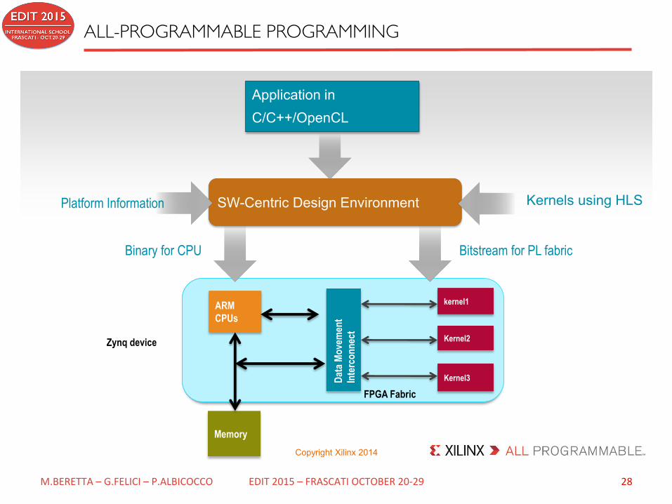
ALL-PROGRAMMABLE PROGRAMMING
EDIT2015–FRASCATIOCTOBER20-29 28M.BERETTA–G.FELICI–P.ALBICOCCO
Copyright Xilinx 2014.
All-Programmable Programming
kernel1ARMCPUs
Kernel2
Kernel3
Memory
Data
Mov
emen
t In
terc
onne
ctZynq device
Binary for CPU Bitstream for PL fabric
Platform Information Kernels using HLSSW-Centric Design Environment
Application in C/C++/OpenCL
FPGA Fabric

A NICE ZYNQ APPLICATION
EDIT2015–FRASCATIOCTOBER20-29 29M.BERETTA–G.FELICI–P.ALBICOCCOCopyright Xilinx 2014
.
2 camerasMicrophone4 motorsAutonomousAvoids obstaclesResponds to audio signals and hand gesturesProgrammable aerial platformProgrammed with OpenCL
37
Phenox
hhp://phenoxlab.com

BIBLIOGRAPHY
EDIT2015–FRASCATIOCTOBER20-29 30M.BERETTA–G.FELICI–P.ALBICOCCO
[1]Programmable ASIC Design - Haibo Wang - ECE Department Southern Illinois University [2] ThreeAgesofFPGAs- SteveTrimberger–Fellow-XilinxResearchLabs[3]IntroducNontoFieldProgrammableGateArrays-IntroducNontoFieldProgrammableGateArrays-CERNAcceleratorSchoolonDigitalSignalProcessing