Embed Size (px)
Citation preview

2-1
Chapter 2
Hardware Installation
This chapter gives you a step-by-step procedure on how to install your system.Follow each section accordingly.
Caution: Electrostatic discharge (ESD) candamage your processor, disk drives, expansionboards, and other components. Alwaysobserve the following precautions before youinstall a system component.
1. Do not remove a component from itsprotective packaging until you are readyto install it.
2. Wear a wrist ground strap and attach it toa metal part of the system unit beforehandling a component. If a wrist strap isnot available, maintain contact with thesystem unit throughout any procedurerequiring ESD protection.

Hardware Installation
2-2
2.1 Jumper and Connector Locations
The following figure shows the locations of the jumpers and connectors on thesystem board:
KB1
PCI1
PCI2
PCI3
ISA1
ISA2
IrDA
HDD LED
PANEL
PWR1
PS2 MSUSB
FDC
PRINTER
COM1
COM2BIOS Super
I/O
DI
MM1
DI
MM2
IDE1 IDE2
5591
SI
MM2
SI
MM1
JP14
5595
AGP
SW1
JP12
JP4
JP5
JP6
CPUFAN1
CPUFAN2
FAN

Hardware Installation
2-3
Jumpers:
SW1: DIP Switch for CPU voltage and clock ratioJP4,JP5,JP6: CPU external (bus) clockJP12: I/O VoltageJP14: Clear CMOS
Connectors:
KB1: AT keyboard connectorPWR1: AT (PS/2) power connectorPS2 MS: PS/2 mouse connectorUSB: USB connectorCOM1: COM1 connectorCOM2: COM2 connectorFDC: Floppy drive connectorPRINTER: Printer connectorIDE1: IDE1 primary channelIDE2: IDE2 secondary channelCPUFAN1: 3-pin CPU fan connectorCPUFAN2: 2-pin CPU fan connectorFAN: 3-pin housing fan connectorIrDA: IrDA (Infrared) connectorHDD LED: HDD LED connectorPANEL: Front panel (Multifunction) connector

Hardware Installation
2-4
2.2 Jumpers
Jumpers are made by pin headers and plastic connecting caps for the purpose ofcustomizing your hardware. Doing so requires basic knowledge of computerhardware, be sure you understand the meaning of the jumpers before you changeany setting. The onboard jumpers are normally set to their default with optimizedsettings.
On the mainboard, normally there is a bold line marked beside pin 1 of thejumper, sometimes, there are numbers also. If we connect (short) plastic cap topin 1 and 2, we will say set it at 1-2, and when we say jumper is open, that meansno plastic cap connected to jumper pins.
12
Open
12
Short
123
Jumper set at 1-2
123
Jumper set at 2-3
For your convenience to install a CPU, this motherboard also use a DIP switch toset CPU voltage and frequency ratio. The following figure simply shows you howto set this DIP switch, please see also to next sections for more details.
ON
1 2 3 4 5 6 7 8
OFF ON
Hardware Installation
2-5
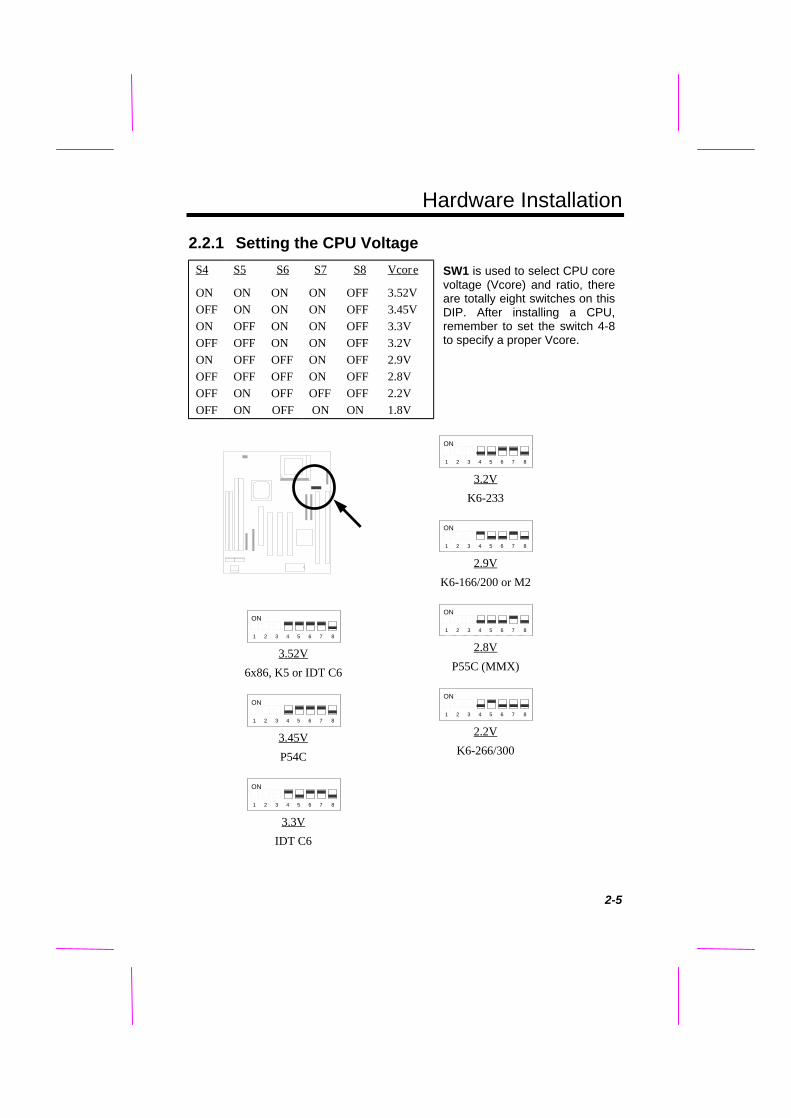
2.2.1 Setting the CPU Voltage
S4
ONOFFONOFFONOFFOFFOFF
S5
ONONOFFOFFOFFOFFONON
S6
ONONONONOFFOFFOFFOFF
S7
ONONONONONONOFFON
S8
OFFOFFOFFOFFOFFOFFOFFON
Vcore
3.52V3.45V3.3V3.2V2.9V2.8V2.2V1.8V
SW1 is used to select CPU corevoltage (Vcore) and ratio, thereare totally eight switches on thisDIP. After installing a CPU,remember to set the switch 4-8to specify a proper Vcore.
ON
1 2 3 4 5 6 7 8
3.52V
6x86, K5 or IDT C6
ON
1 2 3 4 5 6 7 8
3.45V
P54C
ON
1 2 3 4 5 6 7 8
3.3V
IDT C6
ON
1 2 3 4 5 6 7 8
3.2V
K6-233
ON
1 2 3 4 5 6 7 8
2.9V
K6-166/200 or M2
ON
1 2 3 4 5 6 7 8
2.8V
P55C (MMX)
ON
1 2 3 4 5 6 7 8
2.2V
K6-266/300

Hardware Installation
2-6
Warning: Please make sure that you have installed CPU fanproperly if Intel PP/MT-233 or AMD K6 CPU is being selectedto use. It may cause your system unstable if you can not meetthe heat dissipation requirement from above CPU type. It isrecommended to adopt larger fan on these CPU for better airflow in the system. Please refer to AOpen's web site(http://www.aopen.com.tw) to choose a proper CPU fan.
Warning: If your CPU is IDT C6, note that this processorsupports one of two voltage range, 3.135 ~ 3.465V ( 3.45V)and 3.45 ~ 3.6V ( 3.52V). See the CPU specification to set thecorrect voltage.
Tip: Normally, for single voltage CPU, Vcpuio (CPU I/OVoltage) is equal to Vcore, but for CPU that needs dual voltagesuch as PP/MT (P55C) or Cyrix 6x86L, Vcpuio is different fromVcore and must be set to Vio (PBSRAM and Chipset Voltage).The single or dual voltage CPU is automatically detected byhardware circuit.
Tip: For supporting more different CPUs in future, thismotherboard uses five switchs to specify Vcore. There are 32settings totally, and the range is from 1.3V to 3.5V.
CPU Type S4 S5 S6 S7 S8 Vcore
INTEL P54C Single Voltage OFF ON ON ON OFF 3.45V
INTEL MMX P55C Dual Voltage OFF OFF OFF ON OFF 2.8V
AMD K5 Single Voltage ON ON ON ON OFF 3.52V
AMD K6-166/200 Dual Voltage ON OFF OFF ON OFF 2.9V
AMD K6-233 Dual Voltage OFF OFF ON ON OFF 3.2V
AMD K6-266/300 Dual Voltage OFF ON OFF OFF OFF 2.2V
Cyrix 6x86 Single Voltage ON ON ON ON OFF 3.52V
Cyrix 6x86L Dual Voltage OFF OFF OFF ON OFF 2.8V
Cyrix M2 Dual Voltage ON OFF OFF ON OFF 2.9V
IDT C6 Single Voltage ONON
ONOFF
ONON
ONON
OFFOFF
3.52V3.3V
Hardware Installation
2-7
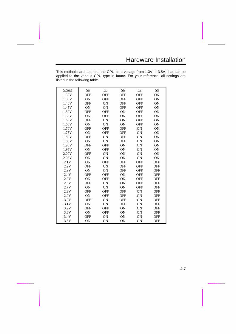
This motherboard supports the CPU core voltage from 1.3V to 3.5V, that can beapplied to the various CPU type in future. For your reference, all settings arelisted in the following table.
Vcore1.30V1.35V1.40V1.45V1.50V1.55V1.60V1.65V1.70V1.75V1.80V1.85V1.90V1.95V2.00V2.05V2.1V2.2V2.3V2.4V2.5V2.6V2.7V2.8V2.9V3.0V3.1V3.2V3.3V3.4V3.5V
S4OFFONOFFONOFFONOFFONOFFONOFFONOFFONOFFONONOFFONOFFONOFFONOFFONOFFONOFFONOFFON
S5OFFOFFONONOFFOFFONONOFFOFFONONOFFOFFONONOFFONONOFFOFFONONOFFOFFONONOFFOFFONON
S6OFFOFFOFFOFFONONONONOFFOFFOFFOFFONONONONOFFOFFOFFONONONONOFFOFFOFFOFFONONONON
S7OFFOFFOFFOFFOFFOFFOFFOFFONONONONONONONONOFFOFFOFFOFFOFFOFFOFFONONONONONONONON
S8ONONONONONONONONONONONONONONONONOFFOFFOFFOFFOFFOFFOFFOFFOFFOFFOFFOFFOFFOFFOFF

Hardware Installation
2-8
JP121-23-4
I/O Voltage (Vio)3.3V (default)3.43V
JP12 is reserved for testing purposes only.This jumper enables you to set the voltage ofthe onboard chipset and PBSRAM (Vio). Fordual-voltage CPU, this jumper also functionsas CPU I/O voltage (Vcpuio) controller.
JP12123
3.3V (default)
JP12123
3.43V
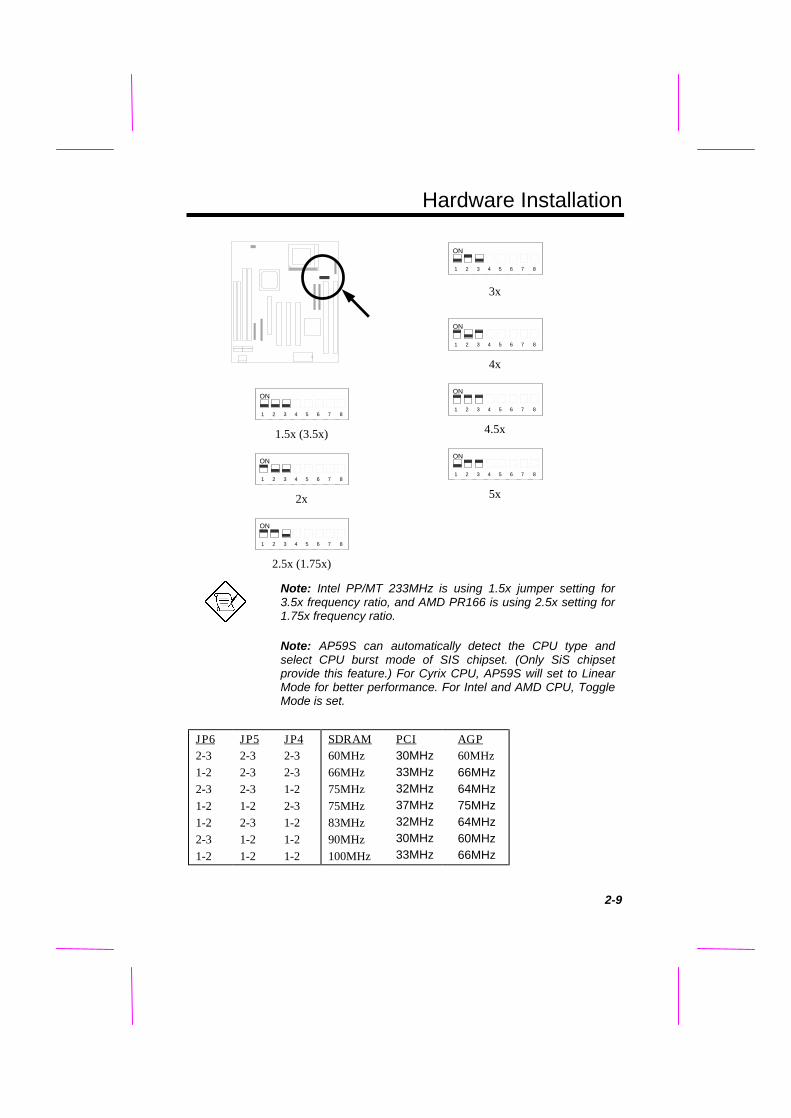
2.2.2 Selecting the CPU Frequency
Intel Pentium, Cyrix 6x86, AMD K5/K6 and IDT C6 CPU are designed to havedifferent Internal (Core) and External (Bus) frequency.
Core frequency = Ratio * External bus clock
S1
OFFONONOFFONONOFF
S2
OFFOFFONONOFFONON
S3
OFFOFFOFFOFFONONON
CPU Frequency Ratio1.5x (3.5x)2x2.5x (1.75x)3x4x4.5x5x
The ratio of Core/Bus frequencyis selected by the switch 1-3 ofSW1.
Note: Intel PP/MT MMX 233MHz is using 1.5x jumper setting for3.5x frequency ratio, and AMD PR166 is using 2.5x setting for1.75x frequency ratio.
Hardware Installation
2-9
ON
1 2 3 4 5 6 7 8
1.5x (3.5x)
ON
1 2 3 4 5 6 7 8
2x
ON
1 2 3 4 5 6 7 8
2.5x (1.75x)
ON
1 2 3 4 5 6 7 8
3x
ON
1 2 3 4 5 6 7 8
4x
ON
1 2 3 4 5 6 7 8
4.5x
ON
1 2 3 4 5 6 7 8
5x
Note: Intel PP/MT 233MHz is using 1.5x jumper setting for3.5x frequency ratio, and AMD PR166 is using 2.5x setting for1.75x frequency ratio.
Note: AP59S can automatically detect the CPU type andselect CPU burst mode of SIS chipset. (Only SiS chipsetprovide this feature.) For Cyrix CPU, AP59S will set to LinearMode for better performance. For Intel and AMD CPU, ToggleMode is set.
JP62-31-22-31-21-22-31-2
JP52-32-32-31-22-31-21-2
JP42-32-31-22-31-21-21-2
SDRAM60MHz66MHz75MHz75MHz83MHz90MHz100MHz
PCI30MHz33MHz32MHz37MHz32MHz30MHz33MHz
AGP60MHz66MHz64MHz75MHz64MHz60MHz66MHz
Hardware Installation
2-10
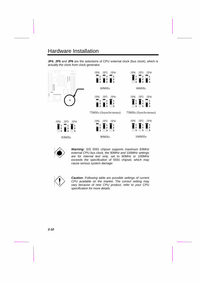
JP4, JP5 and JP6 are the selections of CPU external clock (bus clock), which isactually the clock from clock generator.
JP6 JP5 JP4
123
123
123
83MHz
JP6 JP5 JP4
123
123
123
60MHz
JP6 JP5 JP4
123
123
123
75MHz (Asynchronous)
JP6 JP5 JP4
123
123
123
90MHz
JP6 JP5 JP4
123
123
123
66MHz
JP6 JP5 JP4
123
123
123
75MHz (Synchronous)
JP6 JP5 JP4
123
123
123
100MHz
Warning: SIS 5591 chipset supports maximum 83MHzexternal CPU bus clock, the 90MHz and 100MHz settingsare for internal test only, set to 90MHz or 100MHzexceeds the specification of 5591 chipset, which maycause serious system damage.
Caution: Following table are possible settings of currentCPU available on the market. The correct setting mayvary because of new CPU product, refer to your CPUspecification for more details.

Hardware Installation
2-11
INTELPentium
CPU CoreFrequency
Ratio ExternalBus Clock
S1 S2 S3 JP6 & JP5 & JP4
P54C 90 90MHz = 1.5x 60MHz OFF OFF OFF 2-3 & 2-3 & 2-3
P54C 100 100MHz = 1.5x 66MHz OFF OFF OFF 1-2 & 2-3 & 2-3
P54C 120 120MHz = 2x 60MHz ON OFF OFF 2-3 & 2-3 & 2-3
P54C 133 133MHz = 2x 66MHz ON OFF OFF 1-2 & 2-3 & 2-3
P54C 150 150MHz = 2.5x 60MHz ON ON OFF 2-3 & 2-3 & 2-3
P54C 166 166MHz = 2.5x 66MHz ON ON OFF 1-2 & 2-3 & 2-3
P54C 200 200MHz = 3x 66MHz OFF ON OFF 1-2 & 2-3 & 2-3
INTELPentiumMMX
CPU CoreFrequency
Ratio ExternalBus Clock
S1 S2 S3 JP6 & JP5 & JP4
PP/MT 150 150MHz = 2.5x 60MHz ON ON OFF 2-3 & 2-3 & 2-3
PP/MT 166 166MHz = 2.5x 66MHz ON ON OFF 1-2 & 2-3 & 2-3
PP/MT 200 200MHz = 3x 66MHz OFF ON OFF 1-2 & 2-3 & 2-3
PP/MT 233 233MHz = 3.5x 66MHz OFF OFF OFF 1-2 & 2-3 & 2-3
AMD K5 CPU CoreFrequency
Ratio ExternalBus Clock
S1 S2 S3 JP6 & JP5 & JP4
PR90 90MHz = 1.5x 60MHz OFF OFF OFF 2-3 & 2-3 & 2-3
PR100 100MHz = 1.5x 66MHz OFF OFF OFF 1-2 & 2-3 & 2-3
PR120 90MHz = 1.5x 60MHz OFF OFF OFF 2-3 & 2-3 & 2-3
PR133 100MHz = 1.5x 66MHz OFF OFF OFF 1-2 & 2-3 & 2-3
PR166 116MHz = 1.75x 66MHz ON ON OFF 1-2 & 2-3 & 2-3
AMD K6 CPU CoreFrequency
Ratio ExternalBus Clock
S1 S2 S3 JP6 & JP5 & JP4
PR2-166 166MHz = 2.5x 66MHz ON ON OFF 1-2 & 2-3 & 2-3
PR2-200 200MHz = 3x 66MHz OFF ON OFF 1-2 & 2-3 & 2-3
PR2-233 233MHz = 3.5x 66MHz OFF OFF OFF 1-2 & 2-3 & 2-3
PR2-266 266MHz = 4x 66MHz ON OFF ON 1-2 & 2-3 & 2-3
PR2-300 300MHz = 4.5x 66MHz ON ON ON 1-2 & 2-3 & 2-3
Cyrix 6x86& 6x86L
CPU CoreFrequency
Ratio ExternalBus Clock
S1 S2 S3 JP6 & JP5 & JP4
P150+ 120MHz = 2x 60MHz ON OFF OFF 2-3 & 2-3 & 2-3
P166+ 133MHz = 2x 66MHz ON OFF OFF 1-2 & 2-3 & 2-3
P200+ 150MHz = 2x 75MHz ON OFF OFF 2-3 & 2-3 & 1-2

Hardware Installation
2-12
Cyrix M2 CPU CoreFrequency
Ratio ExternalBus Clock
S1 S2 S3 JP6 & JP5 & JP4
MX-PR166 150MHz = 2.5x 60MHz ON ON OFF 2-3 & 2-3 & 2-3
MX-PR200 166MHz =150MHz =
2.5x2x
66MHz75MHz
ONON
ONOFF
OFFOFF
1-2 & 2-3 & 2-32-3 & 2-3 & 1-2
MX-PR233 200MHz =166MHz =
3x2x
66MHz83.3MHz
OFFON
ONOFF
OFFOFF
1-2 & 2-3 & 2-31-2 & 2-3 & 1-2
MX-PR266 233MHz = 3.5x 66MHz OFF OFF OFF 1-2 & 2-3 & 2-3
MX-PR300 225MHz =233MHz =240MHz =
3x3.5x4x
75MHz66MHz60MHz
OFFOFFON
ONOFFOFF
OFFOFFON
2-3 & 2-3 & 1-21-2 & 2-3 & 2-32-3 & 2-3 & 2-3
IDT C6 CPU CoreFrequency
Ratio ExternalBus Clock
S1 S2 S3 JP6 & JP5 & JP4
C6-150 150MHz = 2x 75MHz ON OFF OFF 2-3 & 2-3 & 1-2
C6-180 180MHz = 3x 60MHz OFF ON OFF 2-3 & 2-3 & 2-3
C6-200 200MHz = 3x 66MHz OFF ON OFF 1-2 & 2-3 & 2-3
C6-225 225MHz = 3x 75MHz OFF ON OFF 2-3 & 2-3 & 1-2
C6-240 240MHz = 4x 60MHz ON OFF ON 2-3 & 2-3 & 2-3
Note: Cyrix 6x86 and AMD K5 CPU use P-ratingfor the reference of CPU benchmark comparedwith INTEL P54C, their internal core frequency isnot exactly equal to P-rating marked on the CPU.For example, Cyrix P166+ is 133MHz butperformance is almost equal to P54C 166MHz andAMD PR133 is 100MHz but performance is almostequal to INTEL P54C 133MHz.
Hardware Installation
2-13
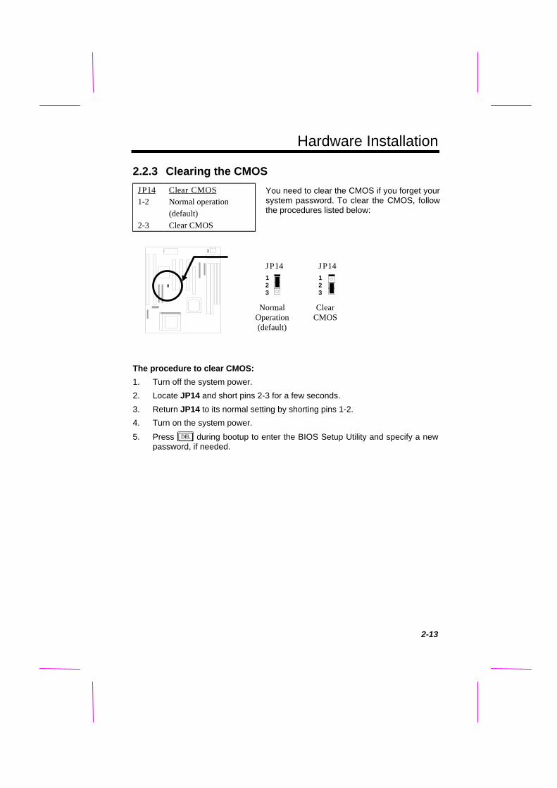
2.2.3 Clearing the CMOS
JP141-2
2-3
Clear CMOSNormal operation(default)Clear CMOS
You need to clear the CMOS if you forget yoursystem password. To clear the CMOS, followthe procedures listed below:
JP14123
NormalOperation(default)
JP14123
ClearCMOS
The procedure to clear CMOS:
1. Turn off the system power.
2. Locate JP14 and short pins 2-3 for a few seconds.
3. Return JP14 to its normal setting by shorting pins 1-2.
4. Turn on the system power.
5. Press during bootup to enter the BIOS Setup Utility and specify a newpassword, if needed.

Hardware Installation
2-14
2.3 Connectors
2.3.1 Power Cable
A standard baby AT (PS/2) power supply has two cables with six wires on each.Plug in these cables to the onboard power connector in such a way that all theblack wires are in the center. The power connector is marked as PWR1 on thesystem board.
Caution: Make sure that the power supply isoff before connecting or disconnecting thepower cable.
Black wire (GND)
Red wire (+5V)
PWR1
2.3.2 CPU Fan
Plug in the fan cable to the fan connectors onboard. The fan connectors aremarked FAN, CPUFAN1 and CPUFAN2 on the system board. You can plug theCPU fan cable to both the 2-pin fan connector FAN and the 3-pin fan connectorCPUFAN1. CPUFAN2 can be reserved for the housing fan. Note that onlyCPUFAN1 and CPUFAN2 supports the fan monitoring function, because 3-pin fanhas an extra pin called SENSE, which periodically sends fan signal out.
+12VSENSEGND
CPUFAN1
CPUFAN2
+12V GND
FAN
Hardware Installation
2-15
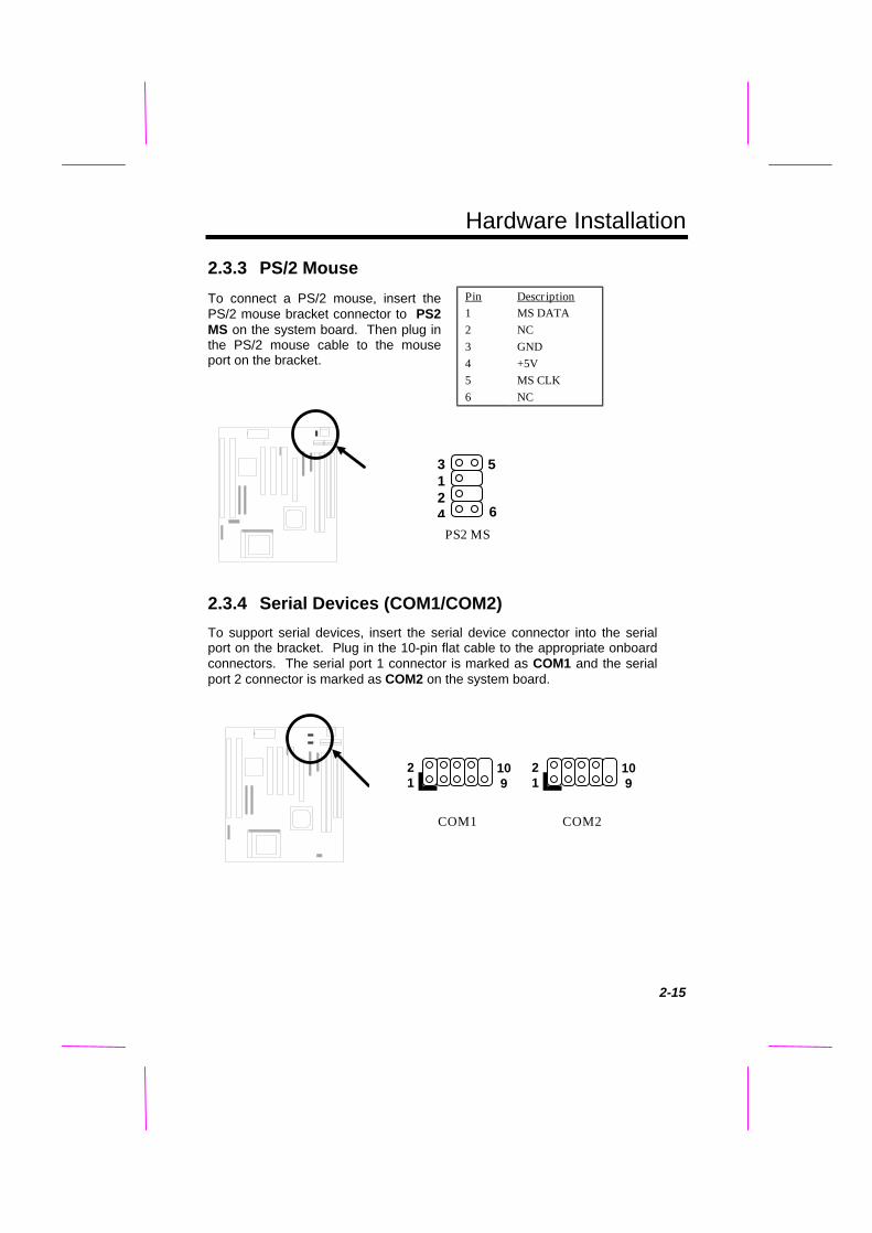
2.3.3 PS/2 Mouse
To connect a PS/2 mouse, insert thePS/2 mouse bracket connector to PS2MS on the system board. Then plug inthe PS/2 mouse cable to the mouseport on the bracket.
Pin123456
DescriptionMS DATANCGND+5VMS CLKNC
3124
5
6
PS2 MS
2.3.4 Serial Devices (COM1/COM2)
To support serial devices, insert the serial device connector into the serialport on the bracket. Plug in the 10-pin flat cable to the appropriate onboardconnectors. The serial port 1 connector is marked as COM1 and the serialport 2 connector is marked as COM2 on the system board.
21
109
COM1
21
109
COM2

Hardware Installation
2-16
2.3.5 USB Device (optional)
You need a USB bracket tohave your system to supportadditional USB device(s). Toattach a USB bracket, simplyinsert the bracket cable to theonboard USB connector markedas USB.
Pin13579
DescriptionV0D0-D0+GNDNC
Pin246810
DescriptionV1D1-D1+GNDNC
1 2
9 10
USB
2.3.6 Floppy Drive
Connect the 34-pin floppy drive cable to the floppy drive connector marked asFDC on the system board.
1
34
2
33
FDC
Hardware Installation
2-17
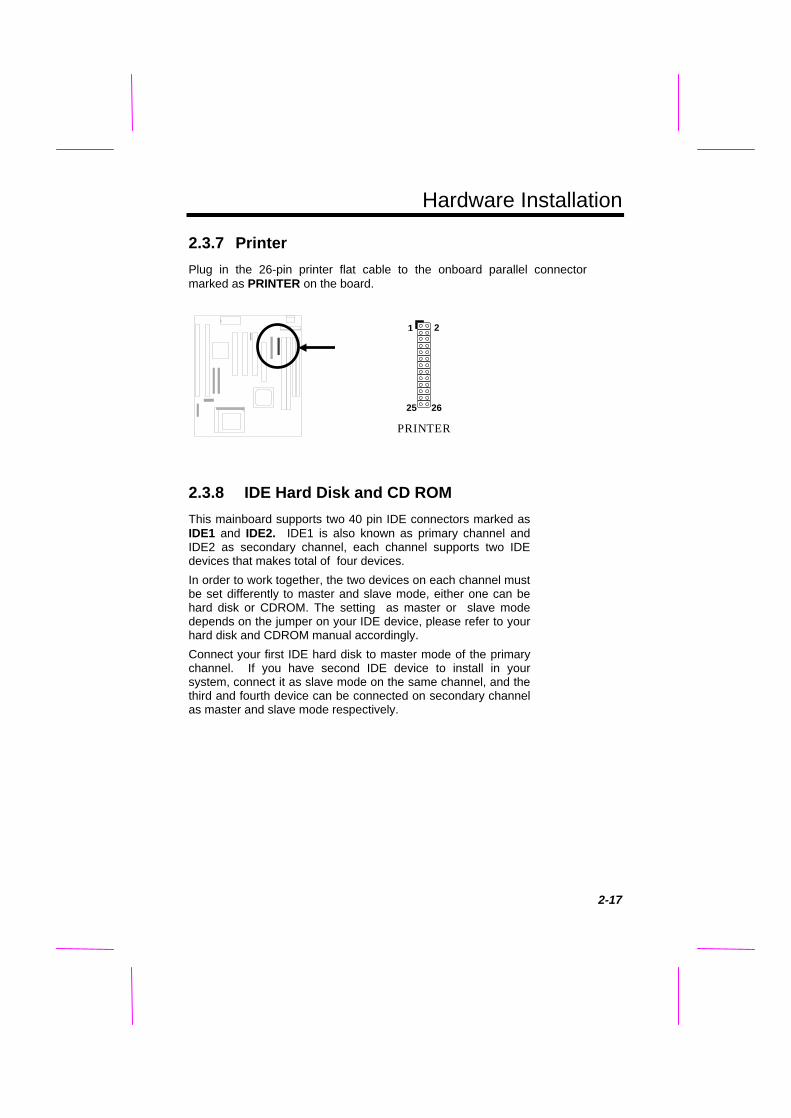
2.3.7 Printer
Plug in the 26-pin printer flat cable to the onboard parallel connectormarked as PRINTER on the board.
1
26
2
25
PRINTER
2.3.8 IDE Hard Disk and CD ROM
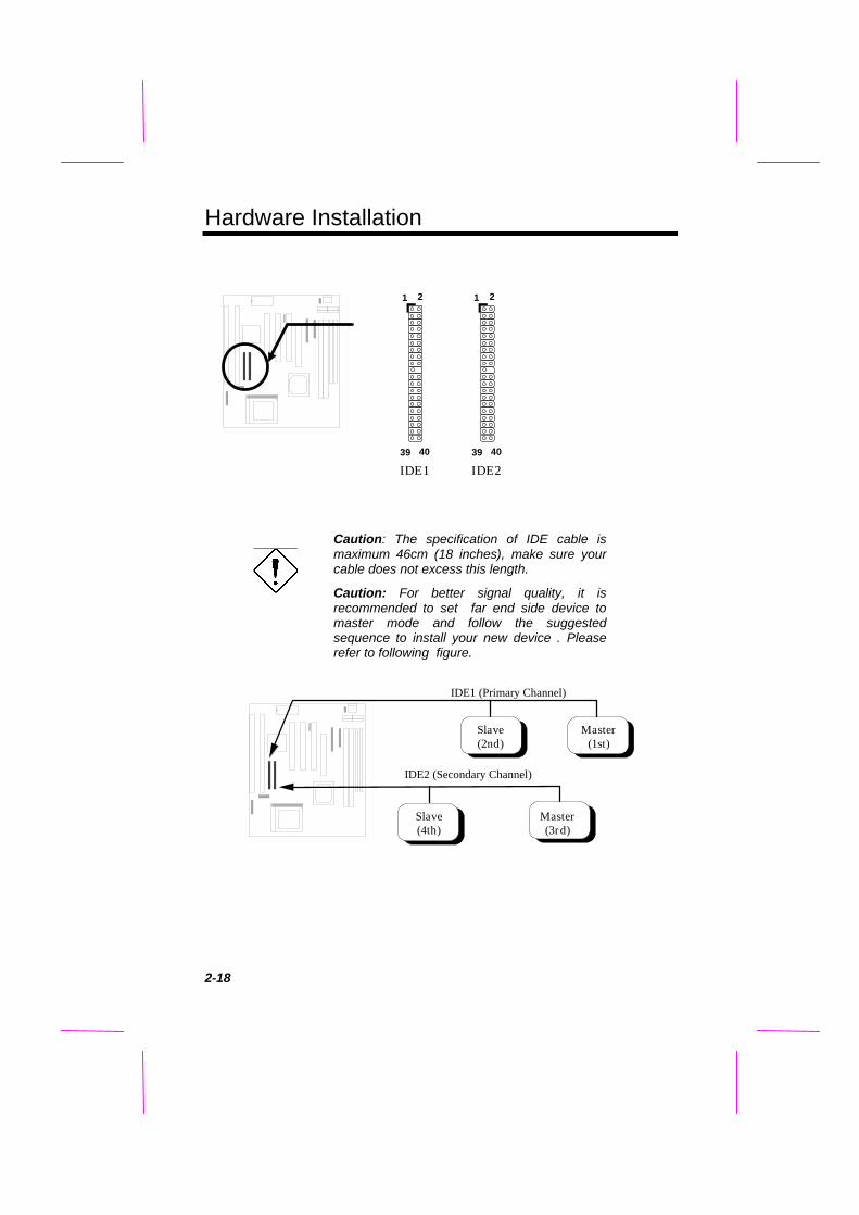
This mainboard supports two 40 pin IDE connectors marked asIDE1 and IDE2. IDE1 is also known as primary channel andIDE2 as secondary channel, each channel supports two IDEdevices that makes total of four devices.
In order to work together, the two devices on each channel mustbe set differently to master and slave mode, either one can behard disk or CDROM. The setting as master or slave modedepends on the jumper on your IDE device, please refer to yourhard disk and CDROM manual accordingly.
Connect your first IDE hard disk to master mode of the primarychannel. If you have second IDE device to install in yoursystem, connect it as slave mode on the same channel, and thethird and fourth device can be connected on secondary channelas master and slave mode respectively.
Hardware Installation
2-18
1
40
2
39
IDE1
1
40
2
39
IDE2
Caution: The specification of IDE cable ismaximum 46cm (18 inches), make sure yourcable does not excess this length.
Caution: For better signal quality, it isrecommended to set far end side device tomaster mode and follow the suggestedsequence to install your new device . Pleaserefer to following figure.
Master(1st)
Slave(2nd)
Master(3rd)
Slave(4th)
IDE1 (Primary Channel)
IDE2 (Secondary Channel)

Hardware Installation
2-19
2.3.9 Hard Disk LED
The HDD LED connector is marked as HDDLED on the board. This connector is designedfor different type of housing, actually only twopins are necessary for the LED. If yourhousing has four pin connector, simply plug itin. If you have only two pin connector, pleaseconnect to pin 1-2 or pin 3-4 according to thepolarity.
Pin
1234
Description
HDD LEDGNDGNDHDD LED
1234
+--+
HDD LED
4-pin connector
1234
+--+
HDD LED
2-pin connectorat pin 1-2
1234
+--+
HDD LED
2-pin connectorat pin 3-4
2.3.10 Panel Connector
The Panel (multifunction) connector is a 20-pin connector marked as PANEL on theboard. Attach the power LED, keylock,speaker, reset switch, and suspend switchconnectors to the corresponding pins asshown in the figure.
Some housings have a five-pin connector forthe keylock and power LED Since powerLED and keylock are aligned together, youcan still use this kind of connector.
1
+5VGNDNCGNDSUSPEND SWSUSPEND SWGNDNCRESETGND
11
10 20
GNDKEYLOCK
GNDRESET
POWER LEDSPEAKER
+5VGND
NCSPEAKER
PANEL

Hardware Installation
2-20
1
Speaker
Power LED
Keylock
Reset
Suspend SW
11
10 20
+
+
+
+
+
PANEL
Other housings may have a 12-pinconnector. If your housing has thistype of connector, connect it toPANEL as shown in the figure. Makesure that the red wire of theconnector is connected to +5V.
1
+5V
11
10 20
PANEL
Note: If your housing comes with Turbo switchconnector, you may use this connector for Suspendswitch functions.
Note: Pressing the Suspend switch allows you tomanually force the system to suspend mode. However,this is possible only if the Power Management function inthe BIOS Setup menu is enabled.

Hardware Installation
2-21
2.3.11 Keyboard
The onboard keyboard connector is a five-pin AT-compatible connector marked asKB1. The view angle of drawing shown here is from back panel of the housing.
Note: The mini DIN PS/2 keyboard connectoris optional.
KB1
PCB

Hardware Installation
2-22
2.3.12 IrDA Connector
Serial port 2 can be configured to support wireless infrared module, withthis module and application software such as Laplink, user can transferfiles to or from laptops, notebooks, PDA and printers. This mainboardsupports IrDA (115Kbps, 1 meter) as well as ASK-IR (19.2Kbps).
Install infrared module onto IrDAconnector and enable infrared functionfrom BIOS setup, make sure to havecorrect orientation when you plug ontoIrDA connector.
Pin123456
Description+5VNCIRRXGNDIRTX+3.3V
Note: Onboard serial port 2 (COM2) will not beavailable after IrDA connector is enabled.
123456
IrDA
Hardware Installation
2-23
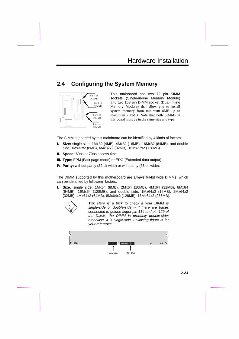
2.4 Configuring the System Memory
Pin 1 ofDIMM1
Pin 1 ofSIMM1
Pin 1 ofSIMM2
Pin 1 ofDIMM2
This mainboard has two 72 pin SIMMsockets (Single-in-line Memory Module)and two 168 pin DIMM socket (Dual-in-lineMemory Module) that allow you to installsystem memory from minimum 8MB up tomaximum 768MB. Note that both SIMMs inthis board must be in the same size and type.
The SIMM supported by this mainboard can be identified by 4 kinds of factors:
I. Size: single side, 1Mx32 (4MB), 4Mx32 (16MB), 16Mx32 (64MB), and doubleside, 1Mx32x2 (8MB), 4Mx32x2 (32MB), 16Mx32x2 (128MB).
II. Speed: 60ns or 70ns access time
III. Type: FPM (Fast page mode) or EDO (Extended data output)
IV. Parity: without parity (32 bit wide) or with parity (36 bit wide).
The DIMM supported by this motherboard are always 64-bit wide DIMMs, whichcan be identified by following factors:
I. Size: single side, 1Mx64 (8MB), 2Mx64 (16MB), 4Mx64 (32MB), 8Mx64(64MB), 16Mx64 (128MB), and double side, 1Mx64x2 (16MB), 2Mx64x2(32MB), 4Mx64x2 (64MB), 8Mx64x2 (128MB), 16Mx64x2 (256MB).
Tip: Here is a trick to check if your DIMM issingle-side or double-side -- if there are tracesconnected to golden finger pin 114 and pin 129 ofthe DIMM, the DIMM is probably double-side;otherwise, it is single-side. Following figure is foryour reference.
168 85
Pin 129 Pin 114

Hardware Installation
2-24
II. Speed:
SDRAM: normally marked as as -12, which means the clock cycle time is 12nsand maximum clock of this SDRAM is 83MHz. Sometimes you can also findthe SDRAM marked as -67, which means maximum clock is 67MHz.
EDO: the access time of EDO RAM can be 60ns or 70ns.
III. Buffered and non-buffered: This motherboard supports non-bufferedDIMMs. You can identify non-buffered DIMMs and buffered DIMMs accordingto the position of the notch, following figure is for your reference:
bufferednon-bufferedReserved
Because the positions are different, only non-buffered DIMMs can be inserted intothe DIMM sockets on this motherboard. Although most of DIMMs on currentmarket are non-buffered, we still recommend you to ask your dealer for thecorrect type.
IV. 2-clock and 4-clock signals: Although both of 2-clock and 4-clock signalsare supported by this motherboard, we strongly recommend you to choose 4-clock SDRAM in consideration of reliability.
Tip: To identify 2-clock and 4-clock SDRAM, youmay check if there are traces connected to goldenfinger pin 79 and pin 163 of the SDRAM. If thereare traces, the SDRAM is probably 4-clock;Otherwise, it is 2-clock.
V. Parity: This motherboard supports standard 64 bit wide (without parity)DIMMs.
VI. SPD support: BIOS will automatically detect DIMM with SPD, and set toappropriate timing. DIMMs without SPD are still able to work fine on thisboard, but BIOS POST screen will give you a warning message that you use aDIMM without SPD.
Hardware Installation
2-25
There is no jumper setting required for the memory size or type. It isautomatically detected by the system BIOS. You can use any single side SIMMand DIMM combination list below for SIMM or DIMM socket, and the total memorysize is to add them together. This motherboard supports maximum 768 MBsystem memory. To achieve this, you may install two 256MB DIMMs and two128MB SIMMs.
SIMM1 SIMM2 Subtotal ofBank0
None None 0MB
4MB 4MB 8MB
8MB 8MB 16MB
16MB 16MB 32MB
32MB 32MB 64MB
64MB 64MB 128MB
128MB 128MB 256MB
DIMM1 Size of DIMM1 DIMM2 Size of DIMM2
None 0MB None 0MB
8MB 8MB 8MB 8MB
16MB 16MB 16MB 16MB
32MB 32MB 32MB 32MB
64MB 64MB 64MB 64MB
128MB 128MB 128MB 128MB
256MB 256MB 256MB 256MB
Total Memory Size = Subtotal of SIMM1 + Subtotal of SIMM2
+ Size of DIMM1 + Size of DIMM2
Warning: It is not recommanded to use SIMM andSDRAM DIMM together unless you have 5V toleranceSDRAM (such as Samsung or TI). The FPM/EDOoperate at 5V while SDRAM operates at 3.3V. If youcombine them together the system will temporary workfine; however after a few months, the SDRAM 3.3V datainput will be damaged by 5V FPM/EDO data output line.
Hardware Installation
2-26
Caution: Make sure that you install the same SIMM typeand size for each bank.
Caution: There are some old DIMMs made by EDO orFPM memory chip, they can only accept 5V power andprobably can not fit into the DIMM socket, make sure youhave 3.3V true SDRAM DIMM before your insert it.
The driving capability of new generation chipset is limited because the lack ofmemory buffer (to improve performance). This makes DRAM chip count animportant factor to be taking into consideration when you install SIMM.Unfortunately, there is no way that BIOS can identified the correct chip count, youneed to calculate the chip count by yourself. The simple rule is: By visualinspection, use only SIMM with chip count less than 24 chips.
Warning: Do not install any SIMM that contains more than 24chips. SIMMs contain more than 24 chips exceed the chipsetdriving specification. Doing so may result in unstable systembehavior.
Warning: Although Intel SIS chipset supports x4 SDRAM chip.Due to loading issue, it is not recommended to use this kind ofSDRAM.
Tip: The SIMM/DIMM chip count can be calculated by followingexample:
1. For 32 bit non-parity SIMM using 1M by 4 bit DRAM chip,32/4=8 chips.
2. For 36 bit parity SIMM using 1M by 4 bit DRAM chip,36/4=9 chips.
3. For 36 bit parity SIMM using 1M by 4 bit and 1M by 1 bitDRAM, the chip count will be 8 data chips(8= 32/4) plus 4parity chips(4=4/1), total is 12 chips.
4. For 64 bit DIMM using 1M by 16 bit SDRAM, the chip countis 64/16=4 chips.

Hardware Installation
2-27
There is an important parameter affects SDRAM performance, CAS LatencyTime. It is similar as CAS Access Time of EDO DRAM and is calculated asnumber of clock state. The SDRAM that AOpen had tested are listed below. Ifyour SDRAM has unstable problem, go into BIOS "Chipset Features Setup",change CAS Latency Time to 3 clocks.
Manufacturer Model Suggested CASLatency Time
5V Tolerance
Samsung KM416511220AT-G12 2 Yes
NEC D4S16162G5-A12-7JF 2 No
Hitachi HM5216805TT10 2 No
Fujitsu 81117822A-100FN 2 No
TI TMX626812DGE-12 2 Yes
TI TMS626812DGE-15 3 Yes
TI TMS626162DGE-15 3 Yes
TI TMS626162DGE-M67 3 Yes
Following table list the recommended DRAM combinations of SIMM and DIMM:
SIMMData chip
SIMMParity chip
Bit sizeper side
Single/Doubleside
Chipcount
SIMMsize
Recommended
1M by 4 None 1Mx32 x1 8 4MB Yes
1M by 4 None 1Mx32 x2 16 8MB Yes
1M by 4 1M by 1 1Mx36 x1 12 4MB Yes
1M by 4 1M by 4 1Mx36 x1 9 4MB Yes
1M by 4 1M by 4 1Mx36 x2 18 8MB Yes
1M by 16 None 1Mx32 x1 2 4MB Yes
1M by 16 None 1Mx32 x2 4 8MB Yes
1M by 16 1M by 4 1Mx36 x1 3 4MB Yes
1M by 16 1M by 4 1Mx36 x2 6 8MB Yes
4M by 4 None 4Mx32 x1 8 16MB Yes
4M by 4 None 4Mx32 x2 16 32MB Yes
4M by 4 4M by 1 4Mx36 x1 12 16MB Yes
4M by 4 4M by 1 4Mx36 x2 24 32MB Yes
Hardware Installation
2-28
SIMMData chip
SIMMParity chip
Bit sizeper side
Single/Doubleside
Chipcount
SIMMsize
Recommended
16M by 4 None 16Mx32 x1 8 64MB Yes, but nottested.
16M by 4 None 16Mx32 x2 16 128MB Yes, but nottested.
16M by 4 16M by 4 16Mx36 x1 9 64MB Yes, but nottested.
16M by 4 16M by 4 16Mx36 x2 18 128MB Yes, but nottested.
DIMMData chip
Bit size perside
Single/Double side
Chipcount
DIMM size Recommended
1M by 16 1Mx64 x1 4 8MB Yes
1M by 16 1Mx64 x2 8 16MB Yes
2M by 8 2Mx64 x1 8 16MB Yes
2M by 8 2Mx64 x2 16 32MB Yes
4M by 16 4Mx64 x2 8 64MB Yes
DIMMData chip
Bit size perside
Single/Double side
Chipcount
DIMM size Recommended
2M by 32 2Mx64 x1 2 16MB Yes, but not tested.
2M by 32 2Mx64 x2 4 32MB Yes, but not tested.
4M by 16 4Mx64 x1 4 32MB Yes, but not tested.
8M by 8 8Mx64 x1 8 64MB Yes, but not tested.
8M by 8 8Mx64 x2 16 128MB Yes, but not tested.
Warning: 64MB SIMMs using 16M by 4 bit chip (64M bittechnology) are not available in the market and are notformally tested by AOpen quality test department yet.However they are supported by design specification fromIntel and they will be tested as soon as they areavailable. Note that 64MB SIMMs using 16M by 1 bitchip (16M bit technology) have chip count exceed 24 andare strongly not recommended.

Hardware Installation
2-29
Tip: 8 bit = 1 byte, 32 bit = 4 byte. The SIMM size isrepresented by number of data byte (whether with orwithout parity), for example, the size of single side SIMMusing 1M by 4 bit chip is 1Mx32 bit, that is, 1M x 4 byte=4MB. For double side SIMM, simply multiply it by 2, thatis, 8MB.
Following table are possible DRAM combinations that is NOT recommended:
SIMMData chip
SIMMParity chip
Bit sizeper side
Single/Doubleside
Chipcount
SIMMsize
Recommended
1M by 1 None 1Mx32 x1 32 4MB No
1M by 1 1M by 1 1Mx36 x1 36 4MB No
1M by 4 1M by 1 1Mx36 x2 24 8MB No
4M by 1 None 4Mx32 x1 32 16MB No
4M by 1 4M by 1 4Mx36 x1 36 16MB No
16M by 1 None 16Mx32 x1 32 64MB No
16M by 1 16M by 1 16Mx36 x1 36 64MB No
DIMMData chip
Bit size perside
Single/Double side
Chipcount
DIMM size Recommended
4M by 4 4Mx64 x1 16 32MB No
4M by 4 4Mx64 x2 32 64MB No
16M by 4 16Mx64 x1 16 128MB No
16M by 4 16Mx64 x2 32 256MB No


![Real-Time Tessellation on GPU [AMD]](https://img.dokumen.tips/doc/110x75/553c8c5e4a7959ac798b4964/real-time-tessellation-on-gpu-amd.jpg)
