Embed Size (px)
Citation preview

AMD-K6MMX Enhanced
Processor
Multimedia Technology
Preliminary Information
TM
TM

Trademarks
AMD, the AMD logo, and combinations thereof are trademarks of Advanced Micro Devices, Inc.
RISC86 is a registered trademark, and K86, AMD-K5, AMD-K6, and the AMD-K6 logo are trademarks of AdvancedMicro Devices, Inc.
Windows NT is a trademark of Microsoft Corporation.
MMX is a trademark of the Intel Corporation.
Other product names used in this publication are for identification purposes only and may be trademarks of their respective companies.
© 2000 Advanced Micro Devices, Inc. All rights reserved.
Advanced Micro Devices, Inc. ("AMD") reserves the right to make changes in itsproducts without notice in order to improve design or performance characteristics.
The information in this publication is believed to be accurate at the time ofpublication, but AMD makes no representations or warranties with respect to theaccuracy or completeness of the contents of this publication or the informationcontained herein, and reserves the right to make changes at any time, withoutnotice. AMD disclaims responsibility for any consequences resulting from the useof the information included in this publication.
This publication neither states nor implies any representations or warranties of anykind, including but not limited to, any implied warranty of merchantability orfitness for a particular purpose. AMD products are not authorized for use as criticalcomponents in life support devices or systems without AMD’s written approval.AMD assumes no liability whatsoever for claims associated with the sale or use(including the use of engineering samples) of AMD products except as provided inAMD’s Terms and Conditions of Sale for such product.
Preliminary Information

20726D/0—January 2000 AMD-K6™ MMX™ Enhanced Processor Multimedia Technology
Preliminary Information
Contents
1 AMD-K6™ Processor Multimedia Technology
Introduction . . . . . . . . . . . . . . . . . . . . . . . . . . . . . . . . . . . . . . . . . . . . . . . 1
Multimedia Technology Architecture. . . . . . . . . . . . . . . . . . . . . . . . . . 2
Key Functionality. . . . . . . . . . . . . . . . . . . . . . . . . . . . . . . . . . . . . 2
Register Set. . . . . . . . . . . . . . . . . . . . . . . . . . . . . . . . . . . . . . . . . . 4
Data Types . . . . . . . . . . . . . . . . . . . . . . . . . . . . . . . . . . . . . . . . . . 6
Instructions . . . . . . . . . . . . . . . . . . . . . . . . . . . . . . . . . . . . . . . . . . 7
Instruction Formats . . . . . . . . . . . . . . . . . . . . . . . . . . . . . . . . . . . 8
2 Programming Considerations
Feature Detection . . . . . . . . . . . . . . . . . . . . . . . . . . . . . . . . . . . . 9
Task Switching . . . . . . . . . . . . . . . . . . . . . . . . . . . . . . . . . . . . . . 11
Exceptions. . . . . . . . . . . . . . . . . . . . . . . . . . . . . . . . . . . . . . . . . . 13
Mixing MMX™ and Floating-Point Instructions . . . . . . . . . . . 14
Prefixes . . . . . . . . . . . . . . . . . . . . . . . . . . . . . . . . . . . . . . . . . . . . 14
3 MMX™ Instruction Set
EMMS . . . . . . . . . . . . . . . . . . . . . . . . . . . . . . . . . . . . . . . . . . . . . 18
MOVD . . . . . . . . . . . . . . . . . . . . . . . . . . . . . . . . . . . . . . . . . . . . . 19
MOVQ . . . . . . . . . . . . . . . . . . . . . . . . . . . . . . . . . . . . . . . . . . . . . 20
PACKSSDW . . . . . . . . . . . . . . . . . . . . . . . . . . . . . . . . . . . . . . . . 21
PACKSSWB. . . . . . . . . . . . . . . . . . . . . . . . . . . . . . . . . . . . . . . . . 23
PACKUSWB . . . . . . . . . . . . . . . . . . . . . . . . . . . . . . . . . . . . . . . . 26
PADDB. . . . . . . . . . . . . . . . . . . . . . . . . . . . . . . . . . . . . . . . . . . . . 29
PADDD . . . . . . . . . . . . . . . . . . . . . . . . . . . . . . . . . . . . . . . . . . . . 31
PADDSB . . . . . . . . . . . . . . . . . . . . . . . . . . . . . . . . . . . . . . . . . . . 33
PADDSW . . . . . . . . . . . . . . . . . . . . . . . . . . . . . . . . . . . . . . . . . . . 35
PADDUSB . . . . . . . . . . . . . . . . . . . . . . . . . . . . . . . . . . . . . . . . . . 37
PADDUSW . . . . . . . . . . . . . . . . . . . . . . . . . . . . . . . . . . . . . . . . . 39
PADDW . . . . . . . . . . . . . . . . . . . . . . . . . . . . . . . . . . . . . . . . . . . . 41
Contents iii

AMD-K6™ MMX™ Enhanced Processor Multimedia Technology 20726D/0—January 2000
Preliminary Information
PAND . . . . . . . . . . . . . . . . . . . . . . . . . . . . . . . . . . . . . . . . . . . . . . 43
PANDN . . . . . . . . . . . . . . . . . . . . . . . . . . . . . . . . . . . . . . . . . . . . 45
PCMPEQB . . . . . . . . . . . . . . . . . . . . . . . . . . . . . . . . . . . . . . . . . . 47
PCMPEQD. . . . . . . . . . . . . . . . . . . . . . . . . . . . . . . . . . . . . . . . . . 49
PCMPEQW . . . . . . . . . . . . . . . . . . . . . . . . . . . . . . . . . . . . . . . . . 51
PCMPGTB . . . . . . . . . . . . . . . . . . . . . . . . . . . . . . . . . . . . . . . . . . 53
PCMPGTD . . . . . . . . . . . . . . . . . . . . . . . . . . . . . . . . . . . . . . . . . . 55
PCMPGTW . . . . . . . . . . . . . . . . . . . . . . . . . . . . . . . . . . . . . . . . . 57
PMADDWD . . . . . . . . . . . . . . . . . . . . . . . . . . . . . . . . . . . . . . . . . 59
PMULHW . . . . . . . . . . . . . . . . . . . . . . . . . . . . . . . . . . . . . . . . . . 61
PMULLW. . . . . . . . . . . . . . . . . . . . . . . . . . . . . . . . . . . . . . . . . . . 63
POR . . . . . . . . . . . . . . . . . . . . . . . . . . . . . . . . . . . . . . . . . . . . . . . 65
PSLLD . . . . . . . . . . . . . . . . . . . . . . . . . . . . . . . . . . . . . . . . . . . . . 67
PSLLQ . . . . . . . . . . . . . . . . . . . . . . . . . . . . . . . . . . . . . . . . . . . . . 69
PSLLW. . . . . . . . . . . . . . . . . . . . . . . . . . . . . . . . . . . . . . . . . . . . . 71
PSRAD. . . . . . . . . . . . . . . . . . . . . . . . . . . . . . . . . . . . . . . . . . . . . 73
PSRAW . . . . . . . . . . . . . . . . . . . . . . . . . . . . . . . . . . . . . . . . . . . . 75
PSRLD . . . . . . . . . . . . . . . . . . . . . . . . . . . . . . . . . . . . . . . . . . . . . 77
PSRLQ . . . . . . . . . . . . . . . . . . . . . . . . . . . . . . . . . . . . . . . . . . . . . 79
PSRLW . . . . . . . . . . . . . . . . . . . . . . . . . . . . . . . . . . . . . . . . . . . . 81
PSUBB . . . . . . . . . . . . . . . . . . . . . . . . . . . . . . . . . . . . . . . . . . . . . 83
PSUBD . . . . . . . . . . . . . . . . . . . . . . . . . . . . . . . . . . . . . . . . . . . . . 85
PSUBSB . . . . . . . . . . . . . . . . . . . . . . . . . . . . . . . . . . . . . . . . . . . . 87
PSUBSW . . . . . . . . . . . . . . . . . . . . . . . . . . . . . . . . . . . . . . . . . . . 89
PSUBUSB . . . . . . . . . . . . . . . . . . . . . . . . . . . . . . . . . . . . . . . . . . 91
PSUBUSW . . . . . . . . . . . . . . . . . . . . . . . . . . . . . . . . . . . . . . . . . . 93
PSUBW . . . . . . . . . . . . . . . . . . . . . . . . . . . . . . . . . . . . . . . . . . . . 95
PUNPCKHBW. . . . . . . . . . . . . . . . . . . . . . . . . . . . . . . . . . . . . . . 97
PUNPCKHDQ . . . . . . . . . . . . . . . . . . . . . . . . . . . . . . . . . . . . . . . 99
PUNPCKHWD . . . . . . . . . . . . . . . . . . . . . . . . . . . . . . . . . . . . . 101
PUNPCKLBW . . . . . . . . . . . . . . . . . . . . . . . . . . . . . . . . . . . . . . 103
PUNPCKLDQ . . . . . . . . . . . . . . . . . . . . . . . . . . . . . . . . . . . . . . 105
PUNPCKLWD . . . . . . . . . . . . . . . . . . . . . . . . . . . . . . . . . . . . . . 107
PXOR . . . . . . . . . . . . . . . . . . . . . . . . . . . . . . . . . . . . . . . . . . . . . 109
iv Contents

20726D/0—January 2000 AMD-K6™ MMX™ Enhanced Processor Multimedia Technology
Preliminary Information
Revision History
Date Rev Description
July 1996 A Initial release.
March 1997 B Removed paragraph from “Mixing MMX™ and Floating-Point Instructions” on page 14 that contained inaccuracies pertaining to floating-point tag words.
June 1997 C Revised stack exception entry in Table 1, “MMX™ Instruction Exceptions,” on page 13 to include Real mode and Virtual-8086 mode.
June 1997 C Revised note 2 on page 13 regarding floating-point exceptions.
June 1997 C Replaced overbar with # to indicate active-Low signals.
June 1997 C Revised document to comply with MMX trademark.
June 1997 C Revised description of EMMS instruction on page 18.
Jan 2000 D Changed mem64 to mem32 for PUNPCKLBW, PUNPCKLWD, and PUNPCKLDQ.
Revision History v

AMD-K6™ MMX™ Enhanced Processor Multimedia Technology 20726D/0—January 2000
Preliminary Information
vi Revision History

20726D/0—January 2000 AMD-K6™ MMX™ Enhanced Processor Multimedia Technology
Preliminary Information
1AMD-K6™ ProcessorMultimedia Technology
Introduction
Next generation PC performance requirements are beingdriven by emerging multimedia and communications software.3D graphics, video, audio, and telephony capabilities areevolving across education, entertainment, and internetapplications. As multimedia applications continue toproliferate in the marketplace, PC systems suppliers are beingchallenged to deliver multimedia-enabled PC solutionscovering all mainstream price/performance points.
In response to the growing need to provide improved PCmultimedia capabilities, the AMD-K6™ MMX™ enhancedprocessor is the first member in the AMD family of processorsto incorporate a robust multimedia technology that is fullysoftware compatible with the MMX™ technology as defined byIntel . This multimedia technology enables scaleablemultimedia capabilities across a broad range of PC systemprice/performance points.
The AMD-K6 processor features a decode-decoupledsuperscalar microarchitecture and state-of-the-art designtechniques to deliver true sixth-generation performance whilemaintaining full x86 binary software compatibility. An x86binary-compatible processor implements the industry-standardx86 instruction set by decoding and executing the x86
AMD-K6™ Processor Multimedia Technology 1

AMD-K6™ MMX™ Enhanced Processor Multimedia Technology 20726D/0—January 2000
Preliminary Information
instruction set as its native mode of operation. Only this nativemode enables delivery of maximum performance when runningPC software.
The AMD-K6 processor delivers leading-edge performance tomainstream PC systems running industry-standard x86software. The AMD-K6 processor implements advanced designtechniques like instruction pre-decoding, dual x86 opcodedecoding, single-cycle internal RISC operations, parallelexecution units, out-of-order execution, data forwarding,register renaming, and dynamic branch prediction. In otherwords, the AMD-K6 is capable of issuing, executing, andretiring multiple x86 instructions per cycle, resulting insuperior scaleable performance.
This document describes the multimedia technology of theAMD-K6 processor, including data types, instructions, andprogramming considerations.
Multimedia Technology Architecture
The multimedia technology in the AMD-K6 MMX enhancedprocessor is designed to accelerate media and communicationapplications. Specialized applications that use music synthesis,speech synthesis, speech recognition, audio and videocompression and decompression, full motion video, 2D and 3Dgraphics, and video conferencing, can take advantage of theAMD-K6 processor multimedia technology. The multimediatechnology implements new instructions, new data types, andpowerful parallel processing (Single Instruction Multiple Data,SIMD) techniques that can significantly increase theperformance of these applications.
Key Functionality
At the lowest levels, multimedia applications (audio, video, 3Dgraphics, and telephony, etc.) contain many similar functions.When these functions are performed on a processor that doesnot have MMX capability, the processor is heavily burdened bythe computational requirements of this information. Processorsexecuting the MMX instructions increase the performance of
2 AMD-K6™ Processor Multimedia Technology

20726D/0—January 2000 AMD-K6™ MMX™ Enhanced Processor Multimedia Technology
Preliminary Information
multimedia applications. This performance increase is a directresult of the increased multimedia bandwidth of the processor.
Multimedia applications must process large amounts of data.Parallel data computing is exemplified by applications thatmanipulate screen pixel information. Instead of acting on onepixel at a time, multimedia technology enables the system toact on multiple pixels simultaneously. This Single InstructionMultiple Data (SIMD) model is a key feature of MMXtechnology.
The AMD-K6 processor multimedia technology architectureincludes four new MMX data types, 57 new MMX instructions,eight new 64-bit MMX registers, and an SIMD processingpipeline. The multimedia technology is compatible withexisting x86 applications.
The 57 new MMX instructions include arithmetic functions,packing and unpacking functions, logical operations, andmoves. These are the basic functions that are most commonlyused in repetitive computational multimedia programs.
Multimedia applications often use smaller operands—8-bit datais commonly used for pixel information and 16-bit data is usedfor audio samples. The new MMX registers allow data to bepacked into 64-bit operands. For example, 8-bit data (1 byte)can be packed in sets of eight in a single 64-bit register, and alleight bytes can be operated on simultaneously by a single MMXinstruction.
For 256-color video modes, this translates to computing eightpixels per instruction. When an entire screen is being re-drawn,these pixel manipulation routines often use highly repetitiveloops. Parallel processing of eight pieces of data can reduce theprocessing time of a code loop by up to a factor of eight.
Multimedia applications frequently multiply and accumulatedata. The multimedia technology provides instructions thatadd, multiply, and even combine these operations. For example,the PMADDWD instruction can multiply and then add words ofdata in a single instruction that uses far less processor cyclesthan the equivalent x86 operations.
AMD-K6™ Processor Multimedia Technology 3

AMD-K6™ MMX™ Enhanced Processor Multimedia Technology 20726D/0—January 2000
Preliminary Information
Executing MMX™ Instructions
A programmer must approach the use of MMX instructionsdifferently, based on whether the code being developed is atthe system level or at the application level. The details of thesedifferences are discussed in “Programming Considerations” onpage 9.
Before using the MMX instructions, the programmer must usethe CPUID instruction to determine if the processor supportsmultimedia technology. See the AMD Processor RecognitionApplication Note, order# 20734, for more information.
Function 1 (EAX=1) of the AMD-K6 processor CPUIDinstruction returns the processor feature bits in the EDXregister. Software can then test bit 23 of the feature bits todetermine if the processor supports the multimedia technology.If bit 23 is set to 1, MMX instructions are supported. AllAMD-K6 processors have bit 23 set. Once it is determined thatmultimedia technology is supported, subsequent code can usethe MMX instructions. Alternatively, the AMD 8000_0001hextended CPUID function can be used to test whether theprocessor supports multimedia technology.
After a module of MMX code has executed, the programmermust empty the MMX state by executing the EMMS command.Because the MMX registers share the floating-point registers,an instruction is needed to prevent MMX code from interferingwith floating-point. The EMMS command clears the multimediastate and resets all the floating-point tag bits. Emptying theMMX state sets the floating-point tag bits to empty (all ones),which marks the MMX/FP registers as invalid and available.
Register Set
The AMD-K6 processor implements eight new 64-bit MMXregisters. These registers are mapped on the floating-pointregisters. As shown in Figure 1 on page 5, the new MMXinstructions refer to these registers as mmreg0 to mmreg7.Mapping the new MMX registers on the floating-point stackenables backwards compatibility for the register saving thatmust occur as a result of task switching.
4 AMD-K6™ Processor Multimedia Technology

20726D/0—January 2000 AMD-K6™ MMX™ Enhanced Processor Multimedia Technology
Preliminary Information
Figure 1. MMX™ Registers
Aliasing the MMX registers onto the floating-point stackregisters provides a safe way to introduce this new technology.Instead of needing to modify operating systems, new MMXapplications can be supported through device drivers, MMXlibraries, or DLL files. See the Programming Considerationssection of this document for more information.
Current operating systems have support for floating-pointoperations. Using the floating-point registers for MMX code isan ingenious way of implementing automatic support for MMXinstructions. Every time the processor executes an MMXinstruction, all the floating-point register tag bits are set to zero(00b=valid). Setting the tag bits after every MMX instructionprevents the processor from having to perform extra tasks.These extra tasks are normally executed on floating-pointregisters when the Tag field is something other than 00b.
If a task switch occurs during an MMX or floating-pointinstruction, the Control Register (CR0) Task Switch (TS) bit isset to 1. The processor then generates an interrupt 7 (int 7Device Not Avai lable) when i t encounters the nextfloating-point or MMX instruction, allowing the operatingsystem to save the state of the MMX/FP registers.
TAG BITS 63 0
mmreg0
mmreg7
mmreg1
mmreg6
mmreg5
mmreg2
mmreg3
mmreg4
xx
xx
xx
xx
xx
xx
xx
xx
AMD-K6™ Processor Multimedia Technology 5

AMD-K6™ MMX™ Enhanced Processor Multimedia Technology 20726D/0—January 2000
Preliminary Information
If there is a task switch when MMX applications are runningwith older applications that do not include MMX instructions,the MMX/FP register state is still saved automatically throughthe int 7 handler.
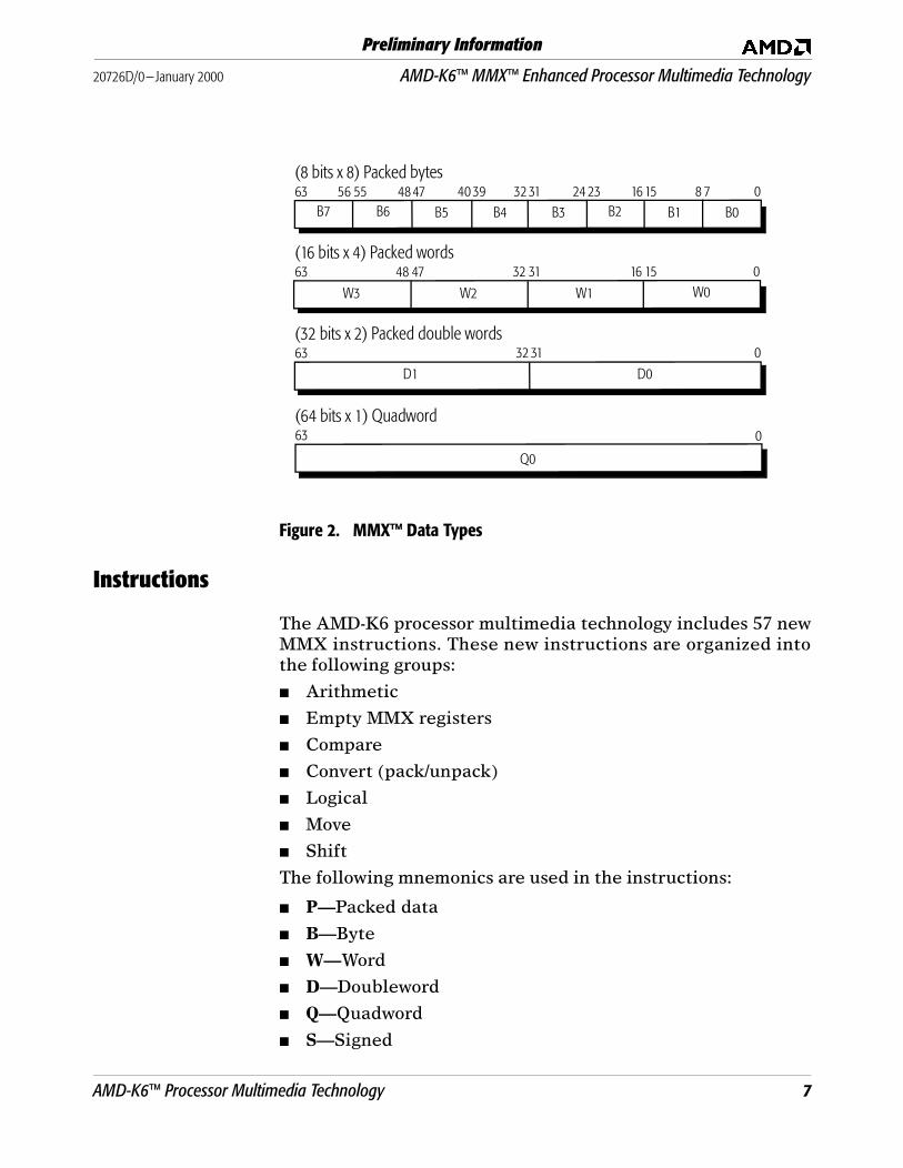
Data Types
The AMD-K6 processor multimedia technology uses a packeddata format. The data is packed in a single, 64-bit MMX registeror memory operand as eight bytes, four words, or two doublewords. Each byte, word, doubleword, or quadword is an integerdata type.
The form of an instruction determines the data type. Forexample, the MOV instruction comes in two different forms—MOVD moves 32 bits of data and MOVQ moves 64 bits of data.
The four new data types are defined as follows:
Packed byte Eight 8-bit bytes packed into 64 bitsSigned integer range(–27 to 27–1)Unsigned integer range(0 to 28–1)
Packed word Four 16-bit words packed into 64-bitsSigned integer range(–215to 215–1)Unsigned integer range(0 to 216–1)
Packed Two 32-bit doublewords packed into 64 bitsdoubleword Signed integer range(–231 to 231–1)
Unsigned integer range(0 to 232–1)
Quadword One 64-bit quadwordSigned integer range(–263 to 263–1)Unsigned integer range(0 to 264–1)
Figure 2 on page 7 shows the four new data types.
6 AMD-K6™ Processor Multimedia Technology
20726D/0—January 2000 AMD-K6™ MMX™ Enhanced Processor Multimedia Technology
Preliminary Information
Figure 2. MMX™ Data Types
Instructions
The AMD-K6 processor multimedia technology includes 57 newMMX instructions. These new instructions are organized intothe following groups:
■ Arithmetic
■ Empty MMX registers
■ Compare
■ Convert (pack/unpack)
■ Logical
■ Move
■ Shift
The following mnemonics are used in the instructions:
■ P—Packed data
■ B—Byte
■ W—Word
■ D—Doubleword
■ Q—Quadword
■ S—Signed
63 56 55 47
63
39 31 23 15 7
47
63
63
31 15
48 40 32 24 16
0
032
48 32 16 0
08
31
(8 bits x 8) Packed bytes
(16 bits x 4) Packed words
(32 bits x 2) Packed double words
(64 bits x 1) Quadword
B2 B1B4 B3B5 B0B6B7
W0W1W2W3
D0D1
Q0
AMD-K6™ Processor Multimedia Technology 7
AMD-K6™ MMX™ Enhanced Processor Multimedia Technology 20726D/0—January 2000
Preliminary Information
■ U—Unsigned
■ SS—Signed Saturation
■ US—Unsigned Saturation
For example, the mnemonic for the PACK instruction that packsfour words into eight unsigned bytes is PACKUSWB. In thismnemonic, the US designates an unsigned result withsaturation, and the WB means that the source is packed wordsand the result is packed bytes.
The term saturation is commonly used in multimediaapplications. Saturation allows mathematical limits to beplaced on the data elements. If a result exceeds the boundary ofthat data type, the result is set to the defined limit for thatinstruction. A common use of saturation is to prevent colorwraparound.
Instruction FormatsAll MMX instructions, except the EMMS instruction that usesno operands, are formatted as follows:
INSTRUCTION mmreg1, mmreg2/mem64
The source operand (mmreg2/mem64) can be either an MMXregister or a memory location. The destination operand(mmreg1) can only be an MMX register.
The MOVD and MOVQ instructions also have the followingacceptable formats:
MOVD mmreg1, mreg32/mem32MOVD mreg32/mem32, mmreg1MOVQ mem64, mmreg1
In the first example, the source operand (mreg32/mem32) canbe either an integer register or a 32-bit memory address. Thedestination operand (mmreg1) can only be an MMX register.The second example has the source operand as an MMXregister. The destination operand (mreg32/mem32) can beeither an integer register or a 32-bit memory address. The thirdexample has the source operand as an MMX register and thedestination operand as a 64-bit memory location
The SHIFT instructions can also utilize an immediate sourceoperand. It is designated as imm8.
PSRLW mmreg1, imm8
8 AMD-K6™ Processor Multimedia Technology

20726D/0—January 2000 AMD-K6™ MMX™ Enhanced Processor Multimedia Technology
Preliminary Information
2Programming Considerations
This chapter describes considerations for programmers writingoperating systems, compilers, and applications that utilizeMMX instructions as implemented in the AMD-K6 MMXenhanced processor.
Feature Detection
To use the AMD-K6 processor multimedia technology, theprogrammer must determine if the processor supports them.The CPUID instruction gives programmers the ability todetermine the presence of multimedia technology on theprocessor. Software must first test to see if the CPUIDinstruction is supported. For a detailed description of theCPUID instruction, see the AMD Processor RecognitionApplication Note, order# 20734.
The presence of the CPUID instruction is indicated by the IDbit (21) in the EFLAGS register. If this bit is writable, theCPUID instruction is supported. The following code sampleshows how to test for the presence of the CPUID instruction.
9

AMD-K6™ MMX™ Enhanced Processor Multimedia Technology 20726D/0—January 2000
Preliminary Information
pushfd ; save EFLAGSpop eax ; store EFLAGS in EAXmov ebx, eax ; save in EBX for later testingxor eax, 00200000h ; toggle bit 21push eax ; put to stackpopfd ; save changed EAX to EFLAGSpushfd ; push EFLAGS to TOSpop eax ; store EFLAGS in EAXcmp eax, ebx ; see if bit 21 has changedjz NO_CPUID ; if no change, no CPUID
If the processor supports the CPUID instruction, theprogrammer must execute the standard function, EAX=0. TheCPUID function returns a 12-character string that identifies theprocessor’s vendor. For AMD processors, standard function 0returns a vendor string of “Authentic AMD”. This stringrequires the software to follow the AMD definitions forsubsequent CPUID functions and the values returned for thosefunctions.
The next step is for the programmer to determine if MMXinstructions are supported. Function 1 of the CPUIDinstruction provides this information. Function 1 (EAX=1) ofthe AMD CPUID instruction returns the feature bits in the EDXregister. If bit 23 in the EDX register is set to 1, MMXinstructions are supported. The following code sample showshow to test for MMX instruction support.
mov eax,1 ; setup function 1CPUID ; call the functiontest edx, 800000 ; test 23rd bitjnz YES_MM ; multimedia technology supported
Alternatively, the extended function 1 (EAX=8000_0001h) canbe used to determine if MMX instructions are supported.
mov eax,8000_0001h ; setup extended function 1CPUID ; call the functiontest edx, 800000 ; test 23rd bitjnz YES_MM ; multimedia technology supported
10 Programming Considerations

20726D/0—January 2000 AMD-K6™ MMX™ Enhanced Processor Multimedia Technology
Preliminary Information
Task SwitchingA task switch is an event that occurs within operating systemsthat allows multiple programs to be executed in parallel. Mostmodern operating systems utilizing task switching, are calledmultitasking operating systems.
There are two types of multitasking operating systems—cooperative and preemptive.
Cooperative Multitasking
In cooperative multitasking operating systems, applications donot care about other tasks that may be running. Each taskassumes that it owns the machine state (processor, registers, I/O,memory, etc.). In addition, these tasks must take care of savingtheir own information (i.e., registers, stacks, states) in their ownmemory areas. The cooperative multitasking operating systemdoes not save operating state information for the applications.
There are different types of cooperative multitasking operatingsystems. Some of these operating systems perform some level ofstate saves, but this state saving is not always reliable. Allsoftware engineers programming for a cooperative multitaskingenvironment must save the MMX or floating-point states beforerelinquishing control to another task or to the operatingsystem. The FSAVE and FRSTOR commands are used toperform this task. Figure 4 illustrates this task switchingprocess.
Note: Some cooperative operating systems may have API calls to perform these tasks for the application.
Figure 3. Cooperative Task Switching
PROGRAM MUST RESTORE STATES
FRSTORcode executingcode module
finishedPROGRAM MUST
SAVE STATES
FSAVEgoto TASK 1
executingMMX™/FP code PROGRAM MUST RESTORE
STATES
FRSTORexecuting code
TASK 1 TASK 2 TASK 1
Task Switch to TASK 2
PROGRAM MUST
SAVE STATES
FSAVE
Programming Considerations 11

AMD-K6™ MMX™ Enhanced Processor Multimedia Technology 20726D/0—January 2000
Preliminary Information
Preemptive Multitasking
In preemptive multitasking operating systems like OS/2,Windows NT™, and UNIX, the operating system handles allstate and register saves. The application programmer does notneed to save states when programming within a preemptivemultitasking environment. The preemptive multitaskingoperating system sets aside a save area for each task.
In a preemptive multitasking operating system, if a task switchoccurs, the operating system sets the Control Register 0 (CR0)Task Switch (TS) bit to 1. If the new task encounters afloating-point or MMX instruction, an interrupt 7 (int 7, DeviceNot Available) is generated. The int7 handler saves the state ofthe first task and restores the state of the second task. The int7handler sets the CR0.TS to 0 and returns to the originalfloating-point or MMX instruction in the second task. Figure 4illustrates this task switching process.
Figure 4. Preemptive Task Switching
executingMMX™/FP code
executing code Save Task 1 State
Restore Task 2
Set CR0.TS=0
Return to Task 2MMX/FP code
TASK 1 TASK 2 INT 7 handler
Task Switch to TASK 2
Set CR0.TS=1
Encounter MMX/FP code
Because TS=1goto INT 7
handler
12 Programming Considerations
20726D/0—January 2000 AMD-K6™ MMX™ Enhanced Processor Multimedia Technology
Preliminary Information
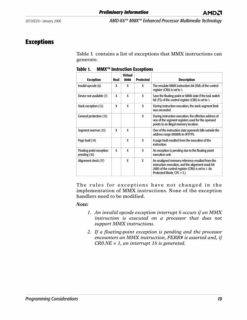
Exceptions
Table 1 contains a list of exceptions that MMX instructions cangenerate.
The rules for except ions have not changed in theimplementation of MMX instructions. None of the exceptionhandlers need to be modified.
Note:
1. An invalid opcode exception interrupt 6 occurs if an MMXinstruction is executed on a processor that does notsupport MMX instructions.
2. If a floating-point exception is pending and the processorencounters an MMX instruction, FERR# is asserted and, ifCR0.NE = 1, an interrupt 16 is generated.
Table 1. MMX™ Instruction Exceptions
Exception RealVirtual8086 Protected Description
Invalid opcode (6) X X X The emulate MMX instruction bit (EM) of the control register (CR0) is set to 1.
Device not available (7) X X X Save the floating-point or MMX state if the task switch bit (TS) of the control register (CR0) is set to 1.
Stack exception (12) X X X During instruction execution, the stack segment limit was exceeded.
General protection (13) X During instruction execution, the effective address of one of the segment registers used for the operand points to an illegal memory location.
Segment overrun (13) X X One of the instruction data operands falls outside the address range 00000h to 0FFFFh.
Page fault (14) X X A page fault resulted from the execution of the instruction.
Floating-point exceptionpending (16)
X X X An exception is pending due to the floating-point execution unit.
Alignment check (17) X X An unaligned memory reference resulted from the instruction execution, and the alignment mask bit (AM) of the control register (CR0) is set to 1. (In Protected Mode, CPL = 3.)
Programming Considerations 13

AMD-K6™ MMX™ Enhanced Processor Multimedia Technology 20726D/0—January 2000
Preliminary Information
Mixing MMX™ and Floating-Point Instructions
The programmer must take care when writing code thatcontains both MMX and floating-point instructions. The MMXcode modules should be separated from the floating-point codemodules. All code of one type (MMX or floating-point code)should be grouped together as often as possible. To obtain thehighest performance, routines should not contain anyconditional branches at the end of loops that jump to code of adifferent type than the code that is currently being executed.
In certain multimedia environments, floating-point and MMXinstructions may be mixed. For example, if a programmer wantsto change the viewing perspective of a three-dimensional scene,the perspective can be changed through transformationmatrices using floating-point registers. The picture/pixelinformation is integer-based and requires MMX instructions tomanipulate this information. Both MMX and floating-pointinstructions are required to perform this task.
The software must clean up after itself at the end of an MMXcode module. The EMMS instruction must be used at the end ofan MMX code module to mark all floating-point registers asempty (11=empty/invalid). In cooperative multitaskingoperating systems, the EMMS instruction must be used whenswitching between tasks.
Note: In some situations, experienced programmers can utilize the MMX registers to pass information between tasks. In these situations, the EMMS instruction is not required.
The tag bits are affected by every MMX and floating-pointinstruction. After every MMX instruction except EMMS, all thetag bits in the floating-point tag word are set to 0. When theEMMS instruction is executed, all the tag bits in the tag wordare set to 1.
Prefixes
All instructions in the x86 architecture translate to a binaryvalue or opcode. This 1 or 2 byte opcode value is different foreach instruction. If an instruction is two bytes long, the secondbyte is called the Mod R/M byte. The Mod R/M byte is used tofurther describe the type of instruction that is used.
14 Programming Considerations

20726D/0—January 2000 AMD-K6™ MMX™ Enhanced Processor Multimedia Technology
Preliminary Information
The x86 opcode and the Mod R/M byte can also be followed byan SIB byte. This byte is used to describe the Scale, Index andBase forms of 32-bit addressing.
The format of the x86 instruction allows for certain prefixes tobe placed before each instruction. These prefixes indicatedifferent types of command overrides.
The MMX instructions follow these rules just like all thecurrent existing instructions. This allows for an easyimplementation into the x86 architecture. All of the rules thatapply to the x86 architecture apply to MMX instructions,including accessing registers, memory, and I/O.
Most opcode prefixes can be utilized while using MMXinstructions. The following prefixes can be used with MMXinstructions:
■ The Segment Override prefixes (2Eh/CS, 36h/SS, 3Eh/DS, 26h/ES, 64h/FS, and 65h/GS) affect MMX instructions that contain a memory operand.
■ The LOCK prefix (F0h) triggers an invalid opcode exception (interrupt 6).
■ The Address Size Override prefix (67h) affects MMX instructions that contain a memory operand.
Programming Considerations 15

AMD-K6™ MMX™ Enhanced Processor Multimedia Technology 20726D/0—January 2000
Preliminary Information
16 Programming Considerations

20726D/0—January 2000 AMD-K6™ MMX™ Enhanced Processor Multimedia Technology
Preliminary Information
3MMX™ Instruction Set
The following MMX instruction definitions are in alphabeticalorder according to the instruction mnemonics.
17

AMD-K6™ MMX™ Enhanced Processor Multimedia Technology 20726D/0—January 2000
Preliminary Information
EMMS
mnemonic opcode description
EMMS 0F 77h Clear the MMX state
Privilege: noneRegisters Affected: MMXFlags Affected: noneExceptions Generated:
The EMMS instruction is used to clear the MMX state following the execution of ablock of code using MMX instructions. Because the MMX registers and tag words areshared with the floating-point unit, it is necessary to clear the state before executingcode that includes floating-point instructions.
Exception RealVirtual 8086 Protected Description
Invalid opcode (6) X X X The emulate MMX instruction bit (EM) of the control register (CR0) is set to 1.
Device not available (7) X X X Save the floating-point or MMX state if the task switch bit (TS) of the con-trol register (CR0) is set to 1.
Floating-point exception pending (16)
X X X An exception is pending due to the floating-point execution unit.
18 MMX™ Instruction Set
20726D/0—January 2000 AMD-K6™ MMX™ Enhanced Processor Multimedia Technology
Preliminary Information
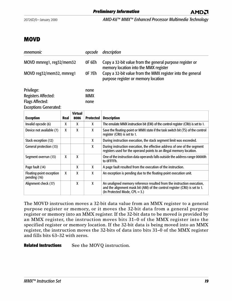
MOVD
mnemonic opcode description
MOVD mmreg1, reg32/mem32 0F 6Eh Copy a 32-bit value from the general purpose register or memory location into the MMX register
MOVD reg32/mem32, mmreg1 0F 7Eh Copy a 32-bit value from the MMX register into the general purpose register or memory location
Privilege: noneRegisters Affected: MMXFlags Affected: noneExceptions Generated:
The MOVD instruction moves a 32-bit data value from an MMX register to a generalpurpose register or memory, or it moves the 32-bit data from a general purposeregister or memory into an MMX register. If the 32-bit data to be moved is provided byan MMX register, the instruction moves bits 31–0 of the MMX register into thespecified register or memory location. If the 32-bit data is being moved into an MMXregister, the instruction moves the 32-bits of data into bits 31–0 of the MMX registerand fills bits 63–32 with zeros.
Related Instructions See the MOVQ instruction.
Exception RealVirtual8086 Protected Description
Invalid opcode (6) X X X The emulate MMX instruction bit (EM) of the control register (CR0) is set to 1.
Device not available (7) X X X Save the floating-point or MMX state if the task switch bit (TS) of the control register (CR0) is set to 1.
Stack exception (12) X During instruction execution, the stack segment limit was exceeded.
General protection (13) X During instruction execution, the effective address of one of the segment registers used for the operand points to an illegal memory location.
Segment overrun (13) X X One of the instruction data operands falls outside the address range 00000h to 0FFFFh.
Page fault (14) X X A page fault resulted from the execution of the instruction.
Floating-point exceptionpending (16)
X X X An exception is pending due to the floating-point execution unit.
Alignment check (17) X X An unaligned memory reference resulted from the instruction execution, and the alignment mask bit (AM) of the control register (CR0) is set to 1.(In Protected Mode, CPL = 3.)
MMX™ Instruction Set 19

AMD-K6™ MMX™ Enhanced Processor Multimedia Technology 20726D/0—January 2000
Preliminary Information
MOVQ
mnemonic opcode description
MOVQ mmreg1, mmreg2/mem64 0F 6Fh Copy a 64-bit value from an MMX register or memory location into an MMX register
MOVQ mmreg2/mem64, mmreg1 0F 7Fh Copy a 64-bit value from an MMX register into an MMX register or memory location
Privilege: noneRegisters Affected: MMXFlags Affected: noneExceptions Generated:
The MOVQ instruction moves a 64-bit data value from one MMX register to anotherMMX register or memory, or it moves the 64-bit data from one MMX register ormemory to another MMX register. Copying data from one memory location to anothermemory location cannot be accomplished with the MOVQ instruction.
Related Instructions See the MOVD instruction.
Exception RealVirtual8086 Protected Description
Invalid opcode (6) X X X The emulate MMX instruction bit (EM) of the control register (CR0) is set to 1.
Device not available (7) X X X Save the floating-point or MMX state if the task switch bit (TS) of the control register (CR0) is set to 1.
Stack exception (12) X During instruction execution, the stack segment limit was exceeded.
General protection (13) X During instruction execution, the effective address of one of the segment registers used for the operand points to an illegal memory location.
Segment overrun (13) X X One of the instruction data operands falls outside the address range 00000h to 0FFFFh.
Page fault (14) X X A page fault resulted from the execution of the instruction.
Floating-point exceptionpending (16)
X X X An exception is pending due to the floating-point execution unit.
Alignment check (17) X X An unaligned memory reference resulted from the instruction execution, and the alignment mask bit (AM) of the control register (CR0) is set to 1.(In Protected Mode, CPL = 3.)
20 MMX™ Instruction Set

20726D/0—January 2000 AMD-K6™ MMX™ Enhanced Processor Multimedia Technology
Preliminary Information
PACKSSDW
mnemonic opcode description
PACKSSDW mmreg1, mmreg2/mem64 0F 6Bh Pack with saturation signed 32-bit operands into signed16-bit results
Privilege: noneRegisters Affected: MMXFlags Affected: noneExceptions Generated:
The PACKSSDW instruction performs a pack and saturate operation on two signed32-bit values in the first operand and two signed 32-bit values in the second operand.The four signed 16-bit results are placed in the specified MMX register.
The pack operation is a data conversion. The PACKSSDW instruction converts orpacks the four signed 32-bit values into four signed 16-bit values, applying saturatingarithmetic. If the signed 32-bit value is less than –32768 (8000h), it saturates to –32768(8000h). If the signed 32-bit value is greater than 32767 (7FFFh), it saturates to 32767(7FFFh). All values between –32768 and 32767 are represented with their signed16-bit value.
The first operand must be an MMX register. In addition to providing the first operand,this MMX register is the location where the result of the pack and saturate operationis stored. The second operand can be an MMX register or a 64-bit memory location.
Exception RealVirtual8086 Protected Description
Invalid opcode (6) X X X The emulate MMX instruction bit (EM) of the control register (CR0) is set to 1.
Device not available (7) X X X Save the floating-point or MMX state if the task switch bit (TS) of the control register (CR0) is set to 1.
Stack exception (12) X During instruction execution, the stack segment limit was exceeded.
General protection (13) X During instruction execution, the effective address of one of the segment registers used for the operand points to an illegal memory location.
Segment overrun (13) X X One of the instruction data operands falls outside the address range 00000h to 0FFFFh.
Page fault (14) X X A page fault resulted from the execution of the instruction.
Floating-point exceptionpending (16)
X X X An exception is pending due to the floating-point execution unit.
Alignment check (17) X X An unaligned memory reference resulted from the instruction execution, and the alignment mask bit (AM) of the control register (CR0) is set to 1.(In Protected Mode, CPL = 3.)
MMX™ Instruction Set 21

AMD-K6™ MMX™ Enhanced Processor Multimedia Technology 20726D/0—January 2000
Preliminary Information
Functional Illustration of the PACKSSDW Instruction
The following list explains the functional illustration of the PACKSSDW instruction:
■ Bits 63–32 of the source operand (mmreg2/mem64) are packed into bits 63–48 ofthe destination operand (mmreg1). The result is saturated to the largest possible16-bit negative number because the 32-bit negative source operand (8000_0002h)exceeds the capacity of the signed 16-bit destination operand.
■ Bits 31–0 of the source operand are packed into bits 47–32 of the destinationoperand. The result is saturated to the largest possible 16-bit positive numberbecause the 32-bit positive source operand (0000_8000h) exceeds the capacity ofthe 16-bit destination operand.
■ Bits 63–32 of the destination operand are packed into bits 31–16 of the destinationoperand. The results are not saturated because the 32-bit negative source operand(FFFF_8002h) does not exceed the capacity of the 16-bit destination operand.
■ Bits 31–0 of the destination operand are packed into bits 15–0 of the destinationoperand. The results are not saturated because the 32-bit positive source operand(0000_01FCh) does not exceed the capacity of the 16-bit destination operand.
Related Instructions See the PACKSSWB instruction.
See the PACKUSWB instruction.
See the PUNPCKHWD instruction.
See the PUNPCKLWD instruction.
00008000
8000h 7FFFh 8002h 01FCh
mmreg1
mmreg2/mem64 mmreg1
00
063
6363
0002h 8000h
3132 3132
31324748 1516
0000FFFF 8002h 01FCh
Indicates a saturated value
22 MMX™ Instruction Set

20726D/0—January 2000 AMD-K6™ MMX™ Enhanced Processor Multimedia Technology
Preliminary Information
PACKSSWB
mnemonic opcode description
PACKSSWB mmreg1, mmreg2/mem64 0F 63h Pack with saturation signed 16-bit operands into signed 8-bitresults
Privilege: noneRegisters Affected: MMXFlags Affected: noneExceptions Generated:
The PACKSSWB instruction performs a pack and saturate operation on four signed16-bit values in the first operand and four signed 16-bit values in the second operand.The eight signed 8-bit results are placed in the specified MMX register.
The pack operation is a data conversion. The PACKSSWB instruction converts orpacks the eight signed 16-bit values into eight signed 8-bit values, applying saturatingarithmetic. If the signed 16-bit value is less than –128 (80h), it saturates to –128 (80h).If the signed 16-bit value is greater than 127 (7Fh), it saturates to 127 (7Fh). All valuesbetween –128 and 127 are represented by their signed 8-bit value.
The first operand must be an MMX register. In addition to providing the first operand,this MMX register is the location where the result of the pack and saturate operationis stored. The second operand can be an MMX register or a 64-bit memory location.
Exception RealVirtual8086 Protected Description
Invalid opcode (6) X X X The emulate MMX instruction bit (EM) of the control register (CR0) is set to 1.
Device not available (7) X X X Save the floating-point or MMX state if the task switch bit (TS) of the control register (CR0) is set to 1.
Stack exception (12) X During instruction execution, the stack segment limit was exceeded.
General protection (13) X During instruction execution, the effective address of one of the segment registers used for the operand points to an illegal memory location.
Segment overrun (13) X X One of the instruction data operands falls outside the address range 00000h to 0FFFFh.
Page fault (14) X X A page fault resulted from the execution of the instruction.
Floating-point exceptionpending (16)
X X X An exception is pending due to the floating-point execution unit.
Alignment check (17) X X An unaligned memory reference resulted from the instruction execution, and the alignment mask bit (AM) of the control register (CR0) is set to 1.(In Protected Mode, CPL = 3.)
MMX™ Instruction Set 23

AMD-K6™ MMX™ Enhanced Processor Multimedia Technology 20726D/0—January 2000
Preliminary Information
Functional Illustration of the PACKSSWB Instruction
The following list explains the functional illustration of the PACKSSWB instruction:
■ Bits 63–48 of the source operand (mmreg2/mem64) are packed into bits 63–56 ofthe destination operand (mmreg1). The result is not saturated because the 16-bitpositive source operand (007Eh) does not exceed the capacity of a signed 8-bitdestination operand.
■ Bits 47–32 of the source operand are packed into bits 55–48 of the destinationoperand. The result is saturated to the largest possible 8-bit positive numberbecause the 16-bit positive source operand (7F00h) exceeds the capacity of asigned 8-bit destination operand.
■ Bits 31–16 of the source operand are packed into bits 47–40 of the destinationoperand. The result is saturated to the largest possible 8-bit negative numberbecause the 16-bit negative source operand (EF9Dh) exceeds the capacity of asigned 8-bit destination operand.
■ Bits 15–0 of the source operand are packed into bits 39–32 of the destinationoperand. The result is not saturated because the 16-bit negative source operand(FF88h) does not exceed the capacity of the 8-bit destination operand.
■ Bits 63–48 of the destination operand are packed into bits 31–24 of the destinationoperand. The result is saturated to the largest possible 8-bit negative numberbecause the 16-bit negative source operand (FF02h) exceeds the capacity of asigned 8-bit destination operand.
00
mmreg1
mmreg2/mem64 mmreg1
00
063
6363
7Eh
3132 3132
31324748 1516
4748 1516 4748 1516
78232439405556
7F 00h EF 9Dh FF 88h FF 02h 00 85h 00 7Eh 81 CFh
7Eh 80h 80h 7Eh7Fh 88h 7Fh 80h
Indicates a saturated value
24 MMX™ Instruction Set

20726D/0—January 2000 AMD-K6™ MMX™ Enhanced Processor Multimedia Technology
Preliminary Information
■ Bits 47–32 of the destination operand are packed into bits 23–16 of the destinationoperand. The result is saturated to the largest possible 8-bit positive numberbecause the 16-bit positive source operand (0085h) exceeds the capacity of asigned 8-bit destination operand.
■ Bits 31–16 of the destination operand are packed into bits 15–8 of the destinationoperand. The result is not saturated because the 16-bit positive source operand(007Eh) does not exceed the capacity of a signed 8-bit destination operand.
■ Bits 15–0 of the destination operand are packed into bits 7–0 of the destinationoperand. The result is saturated to the largest possible 8-bit negative numberbecause the 16-bit negative source operand (81CFh) exceeds the capacity of asigned 8-bit destination operand.
Related Instructions See the PACKSSDW instruction.
See the PACKUSWB instruction.
See the PUNPCKHBW instruction.
See the PUNPCKLBW instruction.
MMX™ Instruction Set 25

AMD-K6™ MMX™ Enhanced Processor Multimedia Technology 20726D/0—January 2000
Preliminary Information
PACKUSWB
mnemonic opcode description
PACKUSWB mmreg1, mmreg2/mem64 0F 67h Pack with saturation signed16-bit operands into unsigned8-bit results
Privilege: noneRegisters Affected: MMXFlags Affected: noneExceptions Generated:
The PACKUSWB instruction performs a pack and saturate operation on four signed16-bit values in the first operand and four signed 16-bit values in the second operand.The eight unsigned 8-bit results are placed in the specified MMX register.
The pack operation is a data conversion. The PACKUSWB instruction converts orpacks the eight signed 16-bit values into eight unsigned 8-bit values, applyingsaturating arithmetic. If the signed 16-bit value is a negative number, it saturates to 0(00h). If the signed 16-bit value is greater than 255 (FFh), it saturates to 255 (FFh). Allvalues between 0 and 255 are represented with their unsigned 8-bit value.
The first operand must be an MMX register. In addition to providing the first operand,this MMX register is the location where the result of the pack and saturate operationis stored. The second operand can be an MMX register or a 64-bit memory location.
Exception RealVirtual8086 Protected Description
Invalid opcode (6) X X X The emulate MMX instruction bit (EM) of the control register (CR0) is set to 1.
Device not available (7) X X X Save the floating-point or MMX state if the task switch bit (TS) of the control register (CR0) is set to 1.
Stack exception (12) X During instruction execution, the stack segment limit was exceeded.
General protection (13) X During instruction execution, the effective address of one of the segment registers used for the operand points to an illegal memory location.
Segment overrun (13) X X One of the instruction data operands falls outside the address range 00000h to 0FFFFh.
Page fault (14) X X A page fault resulted from the execution of the instruction.
Floating-point exceptionpending (16)
X X X An exception is pending due to the floating-point execution unit.
Alignment check (17) X X An unaligned memory reference resulted from the instruction execution, and the alignment mask bit (AM) of the control register (CR0) is set to 1.(In Protected Mode, CPL = 3.)
26 MMX™ Instruction Set

20726D/0—January 2000 AMD-K6™ MMX™ Enhanced Processor Multimedia Technology
Preliminary Information
Functional Illustration of the PACKUSWB Instruction
The following list explains the functional illustration of the PACKUSWB instruction:
■ Bits 63–48 of the source operand (mmreg2/mem64) are packed into bits 63–56 ofthe destination operand (mmreg1). The result is saturated to the largest possible8-bit positive number because the 16-bit positive source operand (0112h) exceedsthe capacity of an unsigned 8-bit destination operand.
■ Bits 47–32 of the source operand are packed into bits 55–48 of the destinationoperand. The result is not saturated because the 16-bit positive source operand(008Bh) does not exceed the capacity of an unsigned 8-bit destination operand.
■ Bits 31–16 of the source operand are packed into bits 47–40 of the destinationoperand. The result is saturated to the largest possible 8-bit positive numberbecause the 16-bit positive source operand exceeds the capacity of an unsigned8-bit destination operand.
■ Bits 15–0 of the source operand are packed into bits 39–32 of the destinationoperand. The result is saturated to 00h because the source operand (FF88h) is anegative value.
■ Bits 63–48 of the destination operand are packed into bits 31–24 of the destinationoperand (mmreg1). The result is not saturated because the 16-bit positive sourceoperand (0002h) does not exceed the capacity of an unsigned 8-bit destinationoperand.
■ Bits 47–32 of the destination operand are packed into bits 23–16 of the destinationoperand. The result is saturated to the largest possible 8-bit positive number
01
mmreg1
mmreg2/mem64 mmreg1
00
063
6363
12h
3132 3132
31324748 1516
4748 1516 4748 1516
78232439405556
00 8Bh 0F 80h FF 88h 00 02h 02 3Ah 00 7Eh FF F8h
FFh FFh 02h 7Eh8Bh 00h FFh 00h
Indicates a saturated value
(Signed) (Signed)
(Unsigned)
MMX™ Instruction Set 27

AMD-K6™ MMX™ Enhanced Processor Multimedia Technology 20726D/0—January 2000
Preliminary Information
because the 16-bit positive source operand (023Ah) exceeds the capacity of anunsigned 8-bit destination operand.
■ Bits 31–16 of the destination operand are packed into bits 15–8 of the destinationoperand. The result is not saturated because the 16-bit positive source operand(007Eh) does not exceed the capacity of an unsigned 8-bit destination operand.
■ Bits 15–0 of the destination operand are packed into bits 7–0 of the destinationoperand. The result is saturated to 00h because the source operand (FFF8h) is anegative value.
Related Instructions See the PACKSSDW instruction.
See the PACKSSWB instruction.
See the PUNPCKHBW instruction.
See the PUNPCKLBW instruction.
28 MMX™ Instruction Set

20726D/0—January 2000 AMD-K6™ MMX™ Enhanced Processor Multimedia Technology
Preliminary Information
PADDB
mnemonic opcode description
PADDB mmreg1, mmreg2/mem64 0F FCh Add unsigned packed 8-bit values
Privilege: noneRegisters Affected: MMXFlags Affected: noneExceptions Generated:
The PADDB instruction adds eight unsigned 8-bit values from the source operand (anMMX register or a 64-bit memory location) to the eight corresponding unsigned 8-bitvalues in the destination operand (an MMX register). If any of the eight results isgreater than the capacity of its 8-bit destination, the value wraps around with no carryinto the next location. The eight 8-bit results are stored in the MMX register that isspecified as the destination operand.
Exception RealVirtual8086 Protected Description
Invalid opcode (6) X X X The emulate MMX instruction bit (EM) of the control register (CR0) is set to 1.
Device not available (7) X X X Save the floating-point or MMX state if the task switch bit (TS) of the controlregister (CR0) is set to 1.
Stack exception (12) X During instruction execution, the stack segment limit was exceeded.
General protection (13) X During instruction execution, the effective address of one of the segmentregisters used for the operand points to an illegal memory location.
Segment overrun (13) X X One of the instruction data operands falls outside the address range 00000hto 0FFFFh.
Page fault (14) X X A page fault resulted from the execution of the instruction.
Floating-point exceptionpending (16)
X X X An exception is pending due to the floating-point execution unit.
Alignment check (17) X X An unaligned memory reference resulted from the instruction execution,and the alignment mask bit (AM) of the control register (CR0) is set to 1.(In Protected Mode, CPL = 3.)
MMX™ Instruction Set 29

AMD-K6™ MMX™ Enhanced Processor Multimedia Technology 20726D/0—January 2000
Preliminary Information
Functional Illustration of the PADDB Instruction
The following list explains the functional illustration of the PADDB instruction:
■ The value 53h is added to ECh and wraps around to 3Fh.
■ The value FCh is added to 14h and wraps around to 10h.
■ The remaining addition operations are simple unsigned operations with nowraparound.
Related Instructions See the PADDD instruction.
See the PADDW instruction.
See the PADDSB instruction.
See the PADDSW instruction.
See the PADDUSB instruction.
See the PADDUSW instruction.
+ + + + + + ++
= = = = = = ==
63 0
63 0
63 0
mmreg2/mem64
mmreg1
mmreg1
00h
00h
00h E2h
00h D0h
12h 1Ah07h
F7h
FEh10h
FCh
14h
3Fh
ECh
53h
42h
42h
FAh
08h
F2h
08h
22h
30 MMX™ Instruction Set

20726D/0—January 2000 AMD-K6™ MMX™ Enhanced Processor Multimedia Technology
Preliminary Information
PADDD
mnemonic opcode description
PADDD mmreg1, mmreg2/mem64 0F FEh Add unsigned packed 32-bit values
Privilege: noneRegisters Affected: MMXFlags Affected: noneExceptions Generated:
The PADDD instruction adds two unsigned 32-bit values from the source operand (anMMX register or a 64-bit memory location) to the two corresponding unsigned 32-bitvalues in the destination operand (an MMX register). If any of the two results isgreater than the capacity of its 32-bit destination, the value wraps around with nocarry into the next location. The two 32-bit results are stored in the MMX registerspecified as the destination operand.
Exception RealVirtual8086 Protected Description
Invalid opcode (6) X X X The emulate MMX instruction bit (EM) of the control register (CR0) is set to 1.
Device not available (7) X X X Save the floating-point or MMX state if the task switch bit (TS) of the controlregister (CR0) is set to 1.
Stack exception (12) X During instruction execution, the stack segment limit was exceeded.
General protection (13) X During instruction execution, the effective address of one of the segmentregisters used for the operand points to an illegal memory location.
Segment overrun (13) X X One of the instruction data operands falls outside the address range 00000hto 0FFFFh.
Page fault (14) X X A page fault resulted from the execution of the instruction.
Floating-point exceptionpending (16)
X X X An exception is pending due to the floating-point execution unit.
Alignment check (17) X X An unaligned memory reference resulted from the instruction execution,and the alignment mask bit (AM) of the control register (CR0) is set to 1.(In Protected Mode, CPL = 3.)
MMX™ Instruction Set 31

AMD-K6™ MMX™ Enhanced Processor Multimedia Technology 20726D/0—January 2000
Preliminary Information
Functional Illustration of the PADDD Instruction
The following list explains the functional illustration of the PADDD instruction:
■ The value FFF0_5C43h is added to 000F_A3BEh and wraps around to 0000_0001h.
■ The second addition is a simple unsigned add operation with no wraparound.
Related Instructions See the PADDB instruction.
See the PADDW instruction.
See the PADDSB instruction.
See the PADDSW instruction.
+ +
= =
mmreg2/mem64
mmreg1
mmreg1
0123_4567h
8000_0000h
8123_4567h0000_0001h
000F_A3BEh
FFF0_5C43h
63 0
63
63
0
0
32 MMX™ Instruction Set

20726D/0—January 2000 AMD-K6™ MMX™ Enhanced Processor Multimedia Technology
Preliminary Information
PADDSB
mnemonic opcode description
PADDSB mmreg1, mmreg2/mem64 0F ECh Add signed packed 8-bit values and saturate
Privilege: noneRegisters Affected: MMXFlags Affected: noneExceptions Generated:
The PADDSB instruction adds eight signed 8-bit values from the source operand (anMMX register or a 64-bit memory location) to the eight corresponding signed 8-bitvalues in the destination operand (an MMX register). If the sum of any two 8-bit valuesis less than –128 (80h), it saturates to –128 (80h). If the sum of any two 8-bit values isgreater than 127 (7Fh), it saturates to 127 (7Fh). The eight signed 8-bit results arestored in the MMX register specified as the destination operand.
Exception RealVirtual8086 Protected Description
Invalid opcode (6) X X X The emulate MMX instruction bit (EM) of the control register (CR0) is set to 1.
Device not available (7) X X X Save the floating-point or MMX state if the task switch bit (TS) of the controlregister (CR0) is set to 1.
Stack exception (12) X During instruction execution, the stack segment limit was exceeded.
General protection (13) X During instruction execution, the effective address of one of the segmentregisters used for the operand points to an illegal memory location.
Segment overrun (13) X X One of the instruction data operands falls outside the address range 00000hto 0FFFFh.
Page fault (14) X X A page fault resulted from the execution of the instruction.
Floating-point exceptionpending (16)
X X X An exception is pending due to the floating-point execution unit.
Alignment check (17) X X An unaligned memory reference resulted from the instruction execution,and the alignment mask bit (AM) of the control register (CR0) is set to 1.(In Protected Mode, CPL = 3.)
MMX™ Instruction Set 33

AMD-K6™ MMX™ Enhanced Processor Multimedia Technology 20726D/0—January 2000
Preliminary Information
Functional Illustration of the PADDSB Instruction
The following list explains the functional illustration of the PADDSB instruction:
■ The signed 8-bit positive value 00h is added to the signed 8-bit positive value 01hwith a signed 8-bit positive result of 01h.
■ The signed 8-bit negative value D2h (–46) is added to the signed 8-bit negativevalue 88h (–120) and saturates to 80h (–128), the largest possible signed 8-bitnegative value.
■ The signed 8-bit positive value 53h (+83) is added to the signed 8-bit negative valueECh (–20) with a signed 8-bit positive result of 3Fh (+63).
■ The signed 8-bit positive value 42h is added to the signed 8-bit positive value 00hwith a signed 8-bit positive result of 42h.
■ The signed 8-bit positive value 77h (+119) is added to the signed 8-bit positivevalue 14h (+20) and saturates to 7Fh (+127), the largest possible positive value.
■ The signed 8-bit positive value 70h (+112) is added to the signed 8-bit positivevalue 44h (+68) and saturates to 7Fh (+127), the largest possible positive value.
■ The signed 8-bit positive value 07h (+7) is added to the signed 8-bit negative valueF7h (–9) with a signed 8-bit negative result of FEh (–2).
■ The signed 8-bit negative value 9Ah (–102) is added to the signed 8-bit negativevalue A8h (–88) and saturates to 80h (–128), the largest possible signed 8-bitnegative value.
Related Instructions See the PADDB instruction.
See the PADDD instruction.
See the PADDW instruction.
See the PADDSW instruction.
+ + + + + + ++
= = = = = = ==
mmreg2/mem64
mmreg1
mmreg1
00h
01h
01h
9Ah
A8h
80h
70h 07h
F7h
FEh
44h
7Fh
77h
14h
7Fh
42h
00h
42h
53h
ECh
3Fh
D2h
88h
80h
63
63
63
0
0
0
Indicates a saturated value
34 MMX™ Instruction Set

20726D/0—January 2000 AMD-K6™ MMX™ Enhanced Processor Multimedia Technology
Preliminary Information
PADDSW
mnemonic opcode description
PADDSW mmreg1, mmreg2/mem64 0F EDh Add signed packed 16-bit values and saturate
Privilege: noneRegisters Affected: MMXFlags Affected: noneExceptions Generated:
The PADDSW instruction adds four signed 16-bit values from the source operand (anMMX register or a 64-bit memory location) to the four corresponding signed 16-bitvalues in the destination operand (an MMX register). If the sum of any two 16-bitvalues is less than –32768 (8000h), it saturates to –32768 (8000h). If the sum of any two16-bit values is greater than 32767 (7FFFh), it saturates to 32767 (7FFFh). The foursigned 16-bit results are stored in the MMX register specified as the destinationoperand.
Exception RealVirtual8086 Protected Description
Invalid opcode (6) X X X The emulate MMX instruction bit (EM) of the control register (CR0) is set to 1.
Device not available (7) X X X Save the floating-point or MMX state if the task switch bit (TS) of the controlregister (CR0) is set to 1.
Stack exception (12) X During instruction execution, the stack segment limit was exceeded.
General protection (13) X During instruction execution, the effective address of one of the segmentregisters used for the operand points to an illegal memory location.
Segment overrun (13) X X One of the instruction data operands falls outside the address range 00000hto 0FFFFh.
Page fault (14) X X A page fault resulted from the execution of the instruction.
Floating-point exceptionpending (16)
X X X An exception is pending due to the floating-point execution unit.
Alignment check (17) X X An unaligned memory reference resulted from the instruction execution,and the alignment mask bit (AM) of the control register (CR0) is set to 1.(In Protected Mode, CPL = 3.)
MMX™ Instruction Set 35

AMD-K6™ MMX™ Enhanced Processor Multimedia Technology 20726D/0—January 2000
Preliminary Information
Functional Illustration of the PADDSW Instruction
The following list explains the functional illustration of the PADDSW instruction:
■ The signed 16-bit negative value D250h (–11696) is added to the signed 16-bitnegative value 8807h (–30713) and saturates to 8000h (–32768), the largest possiblesigned 16-bit negative value.
■ The signed 16-bit positive value 5321h (+21281) is added to the signed 16-bitnegative value EC22h (–5086) with a signed 16-bit positive result of 3F43h(+16195).
■ The signed 16-bit positive value 7007h (+28679) is added to the signed 16-bitpositive value 0FF9h (+4089) and saturates to 7FFFh (+32767), the largest possiblepositive value.
■ The signed 16-bit negative value FFFFh (–1) is added to the signed 16-bit negativevalue FFFFh (–1) with the negative 16-bit result of FFFEh (–2).
Related Instructions See the PADDB instruction.
See the PADDD instruction.
See the PADDW instruction.
See the PADDSB instruction.
See the PADDUSB instruction.
See the PADDUSW instruction.
+ + + +
= = = =
mmreg2/mem64
mmreg1
mmreg1
FFFFhD250h
FFFFh
FFFEh
7007h
0FF9h
7FFFh
5321h
EC22h
3F43h
8807h
8000h
63
63
63
0
0
0
Indicates a saturated value
36 MMX™ Instruction Set

20726D/0—January 2000 AMD-K6™ MMX™ Enhanced Processor Multimedia Technology
Preliminary Information
PADDUSB
mnemonic opcode description
PADDUSB mmreg1, mmreg2/mem64 0F DCh Add unsigned packed 8-bit values and saturate
Privilege: noneRegisters Affected: MMXFlags Affected: noneExceptions Generated:
The PADDUSB instruction adds eight unsigned 8-bit values from the source operand(an MMX register or a 64-bit memory location) to the eight corresponding unsigned8-bit values in the destination operand (an MMX register). The eight unsigned 8-bitresults are stored in the MMX register specified as the destination operand.
If the sum of any two unsigned 8-bit values is greater than 255 (FFh), it saturates to255 (FFh).
Exception RealVirtual8086 Protected Description
Invalid opcode (6) X X X The emulate MMX instruction bit (EM) of the control register (CR0) is set to 1.
Device not available (7) X X X Save the floating-point or MMX state if the task switch bit (TS) of the control register (CR0) is set to 1.
Stack exception (12) X During instruction execution, the stack segment limit was exceeded.
General protection (13) X During instruction execution, the effective address of one of the segment registers used for the operand points to an illegal memory location.
Segment overrun (13) X X One of the instruction data operands falls outside the address range 00000h to 0FFFFh.
Page fault (14) X X A page fault resulted from the execution of the instruction.
Floating-point exceptionpending (16)
X X X An exception is pending due to the floating-point execution unit.
Alignment check (17) X X An unaligned memory reference resulted from the instruction execution, and the alignment mask bit (AM) of the control register (CR0) is set to 1.(In Protected Mode, CPL = 3.)
MMX™ Instruction Set 37

AMD-K6™ MMX™ Enhanced Processor Multimedia Technology 20726D/0—January 2000
Preliminary Information
Functional Illustration of the PADDUSB Instruction
The following list explains the functional illustration of the PADDUSB instruction:
■ The sum of 7Fh and 81h is 100h. This value is greater than FFh, so the resultsaturates to FFh.
■ The sum of D2h and 88h is 15Ah. This value is greater than FFh, so the resultsaturates to FFh.
■ The sum of 53h and ECh is 13Fh. This value is greater than FFh, so the resultsaturates to FFh.
■ The sum of 42h and 0Eh is 50h. This value is not greater than FFh, so the resultdoes not saturate.
■ The sum of 77h and 14h is 8Bh. This value is not greater than FFh, so the resultdoes not saturate.
■ The sum of 70h and 44h is B4h. This value is not greater than FFh, so the resultdoes not saturate.
■ The sum of 07h and F7h is FEh. This value is not greater than FFh, so the resultdoes not saturate.
■ The sum of 9Ah and A8h is 142h. This value is greater than FFh, so the resultsaturates to FFh.
Related Instructions See the PADDB instruction.
See the PADDD instruction.
See the PADDW instruction.
See the PADDSB instruction.
See the PADDSW instruction.
See the PADDUSW instruction.
7Fh D2h 53h 42h 9Ah77h 70h 07hmmreg2/mem64
mmreg1
+ + + + + + ++
= = = = = = ==
FFh FFh FFh 50h FFh8Bh B4h FEhmmreg1
81h 88h ECh 0Eh A8h14h 44h F7h
063
063
063
Indicates a saturated value
38 MMX™ Instruction Set

20726D/0—January 2000 AMD-K6™ MMX™ Enhanced Processor Multimedia Technology
Preliminary Information
PADDUSW
mnemonic opcode description
PADDUSW mmreg1, mmreg2/mem64 0F DDh Add unsigned packed 16-bit values and saturate
Privilege: noneRegisters Affected: MMXFlags Affected: noneExceptions Generated:
The PADDUSW instruction adds four unsigned 16-bit values from the source operand(an MMX register or a 64-bit memory location) to the four corresponding unsigned16-bit values in the destination operand (an MMX register). The four unsigned 16-bitresults are stored in the MMX register specified as the destination operand.
If the sum of any two unsigned 16-bit values is greater than 65,535 (FFFFh), itsaturates to 65,535 (FFFFh).
Exception RealVirtual8086 Protected Description
Invalid opcode (6) X X X The emulate MMX instruction bit (EM) of the control register (CR0) is set to 1.
Device not available (7) X X X Save the floating-point or MMX state if the task switch bit (TS) of the control register (CR0) is set to 1.
Stack exception (12) X During instruction execution, the stack segment limit was exceeded.
General protection (13) X During instruction execution, the effective address of one of the segment registers used for the operand points to an illegal memory location.
Segment overrun (13) X X One of the instruction data operands falls outside the address range 00000h to 0FFFFh.
Page fault (14) X X A page fault resulted from the execution of the instruction.
Floating-point exceptionpending (16)
X X X An exception is pending due to the floating-point execution unit.
Alignment check (17) X X An unaligned memory reference resulted from the instruction execution, and the alignment mask bit (AM) of the control register (CR0) is set to 1.(In Protected Mode, CPL = 3.)
MMX™ Instruction Set 39

AMD-K6™ MMX™ Enhanced Processor Multimedia Technology 20726D/0—January 2000
Preliminary Information
Functional Illustration of the PADDUSW Instruction
The following list explains the functional illustration of the PADDUSW instruction:
■ The sum of 7E10h and 7000h is EE10h. This value is not greater than FFFFh, so theresult does not saturate.
■ The sum of 8000h and 8000h is 10000h. This value is greater than FFFFh, so theresult saturates to FFFFh.
■ The sum of FFFEh and 0015h is 10013h. This value is greater than FFFFh, so theresult saturates to FFFFh.
■ The sum of 1234h and 4567h is 579Bh. This value is not greater than FFFFh, so theresult does not saturate.
Related Instructions See the PADDB instruction.
See the PADDD instruction.
See the PADDW instruction.
See the PADDSB instruction.
See the PADDSW instruction.
See the PADDUSB instruction.
7E10h 8000h FFFEh 1234hmmreg2/mem64
mmreg1 7000h 8000h 0015h 4567h
EE10h FFFFh FFFFh 579Bhmmreg1
+ + + +
= = = =
063
063
063
Indicates a saturated value
40 MMX™ Instruction Set

20726D/0—January 2000 AMD-K6™ MMX™ Enhanced Processor Multimedia Technology
Preliminary Information
PADDW
mnemonic opcode description
PADDW mmreg1, mmreg2/mem64 0F FDh Add unsigned packed 16-bit values
Privilege: noneRegisters Affected: MMXFlags Affected: noneExceptions Generated:
The PADDW instruction adds four unsigned 16-bit values from the source operand (anMMX register or a 64-bit memory location) to the four corresponding unsigned 16-bitvalues in the destination operand (an MMX register). If any of the four results isgreater than the capacity of its 16-bit destination, the value wraps around with nocarry into the next location. The four 16-bit results are stored in the MMX registerspecified as the destination operand.
Exception RealVirtual8086 Protected Description
Invalid opcode (6) X X X The emulate MMX instruction bit (EM) of the control register (CR0) is set to 1.
Device not available (7) X X X Save the floating-point or MMX state if the task switch bit (TS) of the controlregister (CR0) is set to 1.
Stack exception (12) X During instruction execution, the stack segment limit was exceeded.
General protection (13) X During instruction execution, the effective address of one of the segmentregisters used for the operand points to an illegal memory location.
Segment overrun (13) X X One of the instruction data operands falls outside the address range 00000hto 0FFFFh.
Page fault (14) X X A page fault resulted from the execution of the instruction.
Floating-point exceptionpending (16)
X X X An exception is pending due to the floating-point execution unit.
Alignment check (17) X X An unaligned memory reference resulted from the instruction execution,and the alignment mask bit (AM) of the control register (CR0) is set to 1.(In Protected Mode, CPL = 3.)
MMX™ Instruction Set 41
AMD-K6™ MMX™ Enhanced Processor Multimedia Technology 20726D/0—January 2000
Preliminary Information
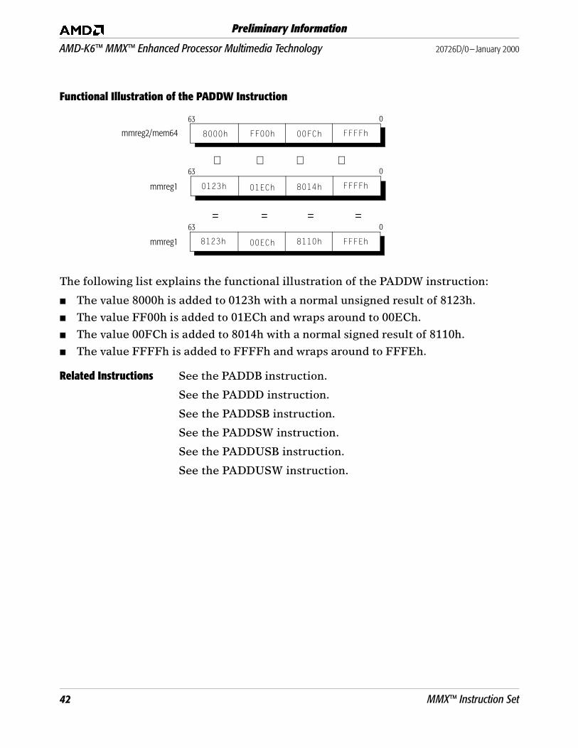
Functional Illustration of the PADDW Instruction
The following list explains the functional illustration of the PADDW instruction:
■ The value 8000h is added to 0123h with a normal unsigned result of 8123h.
■ The value FF00h is added to 01ECh and wraps around to 00ECh.
■ The value 00FCh is added to 8014h with a normal signed result of 8110h.
■ The value FFFFh is added to FFFFh and wraps around to FFFEh.
Related Instructions See the PADDB instruction.
See the PADDD instruction.
See the PADDSB instruction.
See the PADDSW instruction.
See the PADDUSB instruction.
See the PADDUSW instruction.
63
+ + + +
= = = =
mmreg2/mem64
mmreg1
mmreg1
FFFFh
FFFFh
FFFEh
00FCh
8014h
8110h
FF00h
01ECh
8000h
0123h
8123h 00ECh
63
63
0
0
0
42 MMX™ Instruction Set

20726D/0—January 2000 AMD-K6™ MMX™ Enhanced Processor Multimedia Technology
Preliminary Information
PAND
mnemonic opcode description
PAND mmreg1, mmreg2/mem64 0F DBh AND 64-bit values
Privilege: noneRegisters Affected: MMXFlags Affected: noneExceptions Generated:
The PAND instruction operates on the 64-bit source and destination operands tocomplete a bitwise logical AND. The results are stored in the destination operand. Ifthe corresponding bits in the source and destination operands both equal 1, theresulting bit is 1 in the destination. If either bit in the source or destination operandsequals 0, the resulting bit is 0 in the destination.
The PAND instruction can be used to extract operands from packed fields based onthe masks that are produced by the compare instructions—PCMPEQ and PCMPGT.This technique can eliminate branch prediction overhead in MMX routines.
Exception RealVirtual8086 Protected Description
Invalid opcode (6) X X X The emulate MMX instruction bit (EM) of the control register (CR0) is set to 1.
Device not available (7) X X X Save the floating-point or MMX state if the task switch bit (TS) of the control register (CR0) is set to 1.
Stack exception (12) X During instruction execution, the stack segment limit was exceeded.
General protection (13) X During instruction execution, the effective address of one of the segment registers used for the operand points to an illegal memory location.
Segment overrun (13) X X One of the instruction data operands falls outside the address range 00000h to 0FFFFh.
Page fault (14) X X A page fault resulted from the execution of the instruction.
Floating-point exceptionpending (16)
X X X An exception is pending due to the floating-point execution unit.
Alignment check (17) X X An unaligned memory reference resulted from the instruction execution, and the alignment mask bit (AM) of the control register (CR0) is set to 1.(In Protected Mode, CPL = 3.)
MMX™ Instruction Set 43

AMD-K6™ MMX™ Enhanced Processor Multimedia Technology 20726D/0—January 2000
Preliminary Information
Functional Illustration of the PAND Instruction
Related Instructions See the PANDN instruction.
See the POR instruction.
See the PXOR instruction.
1010_1111_0000_1101 0000_1111_0000_1111 1100_0001_0011_0001 1000_1100_1101_0011
0101_1100_1100_0011 1100_1101_0100_1110 1011_0001_0011_1001 0110_0011_0101_1001
0000_1100_0000_0001 0000_1101_0000_1110 1000_0001_0011_0001 0000_0000_0101_0001
mmreg1
032 3163 4748 1516
032 3163 4748 1516
mmreg2/mem64
Logical AND Logical AND Logical AND Logical AND
mmreg1
032 3163 4748 1516
Result
44 MMX™ Instruction Set

20726D/0—January 2000 AMD-K6™ MMX™ Enhanced Processor Multimedia Technology
Preliminary Information
PANDN
mnemonic opcode description
PANDN mmreg1, mmreg2/mem64 0F DFh Invert a 64-bit value, then AND the inverted value and a 64-bit value in memory or an MMX register
Privilege: noneRegisters Affected: MMXFlags Affected: noneExceptions Generated:
The PANDN instruction first operates on the 64-bit destination operand (an MMXregister) to complete a bitwise logical NOT, inverting each bit. This operation changes1 bits to 0 bits and 0 bits to 1 bits, storing the results in the destination operand. Theinverted 64-bit destination operand is then logically AND’d with the 64-bit sourceoperand (an MMX register or a 64-bit memory operand) to complete the PANDNoperation.
If corresponding bits in the source operand and the inverted destination operand areboth 1, the resulting bit is 1 in the destination. If either bit in the source operand orthe inverted destination operand is 0, the resulting bit is 0 in the destination.
The PANDN instruction can be used to extract alternate operands from packed fieldsbased on the inverse of the masks that are produced by the compare instructions—PCMPEQ and PCMPGT. This technique can eliminate branch prediction overhead inMMX routines.
Exception RealVirtual8086 Protected Description
Invalid opcode (6) X X X The emulate MMX instruction bit (EM) of the control register (CR0) is set to 1.
Device not available (7) X X X Save the floating-point or MMX state if the task switch bit (TS) of the control register (CR0) is set to 1.
Stack exception (12) X During instruction execution, the stack segment limit was exceeded.
General protection (13) X During instruction execution, the effective address of one of the segment registers used for the operand points to an illegal memory location.
Segment overrun (13) X X One of the instruction data operands falls outside the address range 00000h to 0FFFFh.
Page fault (14) X X A page fault resulted from the execution of the instruction.
Floating-point exceptionpending (16)
X X X An exception is pending due to the floating-point execution unit.
Alignment check (17) X X An unaligned memory reference resulted from the instruction execution, and the alignment mask bit (AM) of the control register (CR0) is set to 1.(In Protected Mode, CPL = 3.)
MMX™ Instruction Set 45

AMD-K6™ MMX™ Enhanced Processor Multimedia Technology 20726D/0—January 2000
Preliminary Information
Functional Illustration of the PANDN Instruction
Related Instructions See the PAND instruction.
See the POR instruction.
See the PXOR instruction.
1010_1111_0000_1101 0000_1111_0000_1111 1100_0001_0011_0001 1000_1100_1101_0011
0101_1100_1100_0011 1100_1101_0100_1110 1011_0001_0011_1001 0110_0011_0101_1001
0101_0000_1111_0010 1111_0000_1111_0000 0011_1110_1100_1110 0111_0011_0010_1100
0101_0000_1100_0010 1100_0000_0100_0000 0011_0000_0000_1000 0110_0011_0000_1000
mmreg1
032 3163 4748 1516
mmreg1
032 3163 4748 1516
Invert Invert InvertInvert
032 3163 4748 1516
mmreg2/mem64
Logical AND Logical AND Logical AND Logical AND
mmreg1
032 3163 4748 1516
Result
46 MMX™ Instruction Set

20726D/0—January 2000 AMD-K6™ MMX™ Enhanced Processor Multimedia Technology
Preliminary Information
PCMPEQB
mnemonic opcode description
PCMPEQB mmreg1, mmreg2/mem64 0F 74h Compare packed 8-bit values for equality
Privilege: noneRegisters Affected: MMXFlags Affected: noneExceptions Generated:
The PCMPEQB instruction operates on 8-bit data values. The instruction comparestwo 8-bit values to determine if they are equal.
If the corresponding bits in the two operands are equal, all the bits in that 8 bits of thedestination operand are set to 1. If any of the corresponding bits in the two operandsare not equal, all the bits in that 8 bits of the destination operand are set to 0.
Exception RealVirtual8086 Protected Description
Invalid opcode (6) X X X The emulate MMX instruction bit (EM) of the control register (CR0) is set to 1.
Device not available (7) X X X Save the floating-point or MMX state if the task switch bit (TS) of the control register (CR0) is set to 1.
Stack exception (12) X During instruction execution, the stack segment limit was exceeded.
General protection (13) X During instruction execution, the effective address of one of the segment registers used for the operand points to an illegal memory location.
Segment overrun (13) X X One of the instruction data operands falls outside the address range 00000h to 0FFFFh.
Page fault (14) X X A page fault resulted from the execution of the instruction.
Floating-point exceptionpending (16)
X X X An exception is pending due to the floating-point execution unit.
Alignment check (17) X X An unaligned memory reference resulted from the instruction execution, and the alignment mask bit (AM) of the control register (CR0) is set to 1.(In Protected Mode, CPL = 3.)
MMX™ Instruction Set 47

AMD-K6™ MMX™ Enhanced Processor Multimedia Technology 20726D/0—January 2000
Preliminary Information
Functional Illustration of the PCMPEQB Instruction
Related Instructions See the PCMPEQD instruction.
See the PCMPEQW instruction.
See the PCMPGTB instruction.
See the PCMPGTD instruction.
See the PCMPGTW instruction.
DBh 15h 43h FFhmmreg2/mem64
mmreg1
mmreg1
Compare CompareCompare Compare
FalseTrue True False
3163
80h CEh A1h 04h
Compare Compare Compare Compare
032
DDh 15h 42h FFh
3163
80h EEh A1h 14h
032
00h FFh 00h FFh
3163
00hFFh FFh 00h
032
Result ResultResult Result Result Result Result Result
False True False True
48 MMX™ Instruction Set

20726D/0—January 2000 AMD-K6™ MMX™ Enhanced Processor Multimedia Technology
Preliminary Information
PCMPEQD
mnemonic opcode description
PCMPEQD mmreg1, mmreg2/mem64 0F 76h Compare packed 32-bit values for equality
Privilege: noneRegisters Affected: MMXFlags Affected: noneExceptions Generated:
The PCMPEQD instruction operates on 32-bit data values. The instruction comparestwo 32-bit values to determine if they are equal.
If the corresponding bits in the two operands are equal, all the bits in that 32 bits of thedestination operand are set to 1. If any of the corresponding bits in the two operandsare not equal, all the bits in that 32 bits of the destination operand are set to 0.
Exception RealVirtual8086 Protected Description
Invalid opcode (6) X X X The emulate MMX instruction bit (EM) of the control register (CR0) is set to 1.
Device not available (7) X X X Save the floating-point or MMX state if the task switch bit (TS) of the control register (CR0) is set to 1.
Stack exception (12) X During instruction execution, the stack segment limit was exceeded.
General protection (13) X During instruction execution, the effective address of one of the segment registers used for the operand points to an illegal memory location.
Segment overrun (13) X X One of the instruction data operands falls outside the address range 00000h to 0FFFFh.
Page fault (14) X X A page fault resulted from the execution of the instruction.
Floating-point exceptionpending (16)
X X X An exception is pending due to the floating-point execution unit.
Alignment check (17) X X An unaligned memory reference resulted from the instruction execution, and the alignment mask bit (AM) of the control register (CR0) is set to 1.(In Protected Mode, CPL = 3.)
MMX™ Instruction Set 49

AMD-K6™ MMX™ Enhanced Processor Multimedia Technology 20726D/0—January 2000
Preliminary Information
Functional Illustration of the PCMPEQD Instruction
Related Instructions See the PCMPEQB instruction.
See the PCMPEQW instruction.
See the PCMPGTB instruction.
See the PCMPGTD instruction.
See the PCMPGTW instruction.
0000BA14h EF031243hmmreg2/mem64
mmreg1 0000BA13h EF031243h
00000000h FFFFFFFFhmmreg1
Compare Compare
Result Result
False True
063
063
063
50 MMX™ Instruction Set

20726D/0—January 2000 AMD-K6™ MMX™ Enhanced Processor Multimedia Technology
Preliminary Information
PCMPEQW
mnemonic opcode description
PCMPEQW mmreg1, mmreg2/mem64 0F 75h Compare packed 16-bit values for equality
Privilege: noneRegisters Affected: MMXFlags Affected: noneExceptions Generated
The PCMPEQW instruction operates on 16-bit data values. The instruction comparestwo 16-bit values to determine if they are equal.
If the corresponding bits in the two operands are equal, all the bits in that 16 bits of thedestination operand are set to 1. If any of the corresponding bits in the two operandsare not equal, all the bits in that 16 bits of the destination operand are set to 0.
Exception RealVirtual8086 Protected Description
Invalid opcode (6) X X X The emulate MMX instruction bit (EM) of the control register (CR0) is set to 1.
Device not available (7) X X X Save the floating-point or MMX state if the task switch bit (TS) of the control register (CR0) is set to 1.
Stack exception (12) X During instruction execution, the stack segment limit was exceeded.
General protection (13) X During instruction execution, the effective address of one of the segment registers used for the operand points to an illegal memory location.
Segment overrun (13) X X One of the instruction data operands falls outside the address range 00000h to 0FFFFh.
Page fault (14) X X A page fault resulted from the execution of the instruction.
Floating-point exceptionpending (16)
X X X An exception is pending due to the floating-point execution unit.
Alignment check (17) X X An unaligned memory reference resulted from the instruction execution, and the alignment mask bit (AM) of the control register (CR0) is set to 1.(In Protected Mode, CPL = 3.)
MMX™ Instruction Set 51

AMD-K6™ MMX™ Enhanced Processor Multimedia Technology 20726D/0—January 2000
Preliminary Information
Functional Illustration of the PCMPEQW Instruction
Related Instructions See the PCMPEQB instruction.
See the PCMPEQD instruction.
See the PCMPGTB instruction.
See the PCMPGTD instruction.
See the PCMPGTW instruction.
DA14h 8000h 1243h 1234hmmreg2/mem64
mmreg1 DA24h 8000h 1243h 1243h
0000h FFFFh FFFFh 0000hmmreg1
Compare Compare Compare Compare
Result Result Result Result
False True True False
063
063
063
52 MMX™ Instruction Set
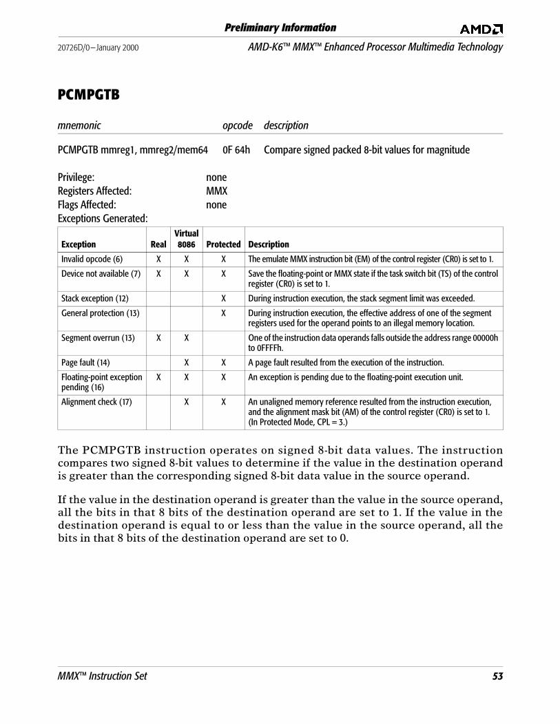
20726D/0—January 2000 AMD-K6™ MMX™ Enhanced Processor Multimedia Technology
Preliminary Information
PCMPGTB
mnemonic opcode description
PCMPGTB mmreg1, mmreg2/mem64 0F 64h Compare signed packed 8-bit values for magnitude
Privilege: noneRegisters Affected: MMXFlags Affected: noneExceptions Generated:
The PCMPGTB instruction operates on signed 8-bit data values. The instructioncompares two signed 8-bit values to determine if the value in the destination operandis greater than the corresponding signed 8-bit data value in the source operand.
If the value in the destination operand is greater than the value in the source operand,all the bits in that 8 bits of the destination operand are set to 1. If the value in thedestination operand is equal to or less than the value in the source operand, all thebits in that 8 bits of the destination operand are set to 0.
Exception RealVirtual8086 Protected Description
Invalid opcode (6) X X X The emulate MMX instruction bit (EM) of the control register (CR0) is set to 1.
Device not available (7) X X X Save the floating-point or MMX state if the task switch bit (TS) of the control register (CR0) is set to 1.
Stack exception (12) X During instruction execution, the stack segment limit was exceeded.
General protection (13) X During instruction execution, the effective address of one of the segment registers used for the operand points to an illegal memory location.
Segment overrun (13) X X One of the instruction data operands falls outside the address range 00000h to 0FFFFh.
Page fault (14) X X A page fault resulted from the execution of the instruction.
Floating-point exceptionpending (16)
X X X An exception is pending due to the floating-point execution unit.
Alignment check (17) X X An unaligned memory reference resulted from the instruction execution, and the alignment mask bit (AM) of the control register (CR0) is set to 1.(In Protected Mode, CPL = 3.)
MMX™ Instruction Set 53

AMD-K6™ MMX™ Enhanced Processor Multimedia Technology 20726D/0—January 2000
Preliminary Information
Functional Illustration of the PCMPGTB Instruction
The following list explains the functional illustration of the PCMPGTB instruction:
■ The negative value DDh (–35) is greater than the negative value DCh (–36), so theresult is true (FFh).
■ The positive value 24h (+36) is not greater than the positive value 25h (+37), so theresult is false (00h).
■ The positive value 42h (+66) is greater than the positive value 41h (+65), so theresult is true (FFh).
■ The positive value 01h (+1) is greater than the negative value FFh (–1), so theresult is true (FFh).
■ The negative value 80h (–128) is not greater than the negative value 80h (–128), sothe result is false (00h).
■ The negative value 80h (–128) is not greater than the positive value 7Fh (+127), sothe result is false (00h).
■ The negative value A3h (–93) is not greater than the negative value A6h (–90), sothe result is false (00h).
■ The positive value 14h (+20) is greater than the positive value 04h (+4), so theresult is true (FFh).
Related Instructions See the PCMPEQB instruction.
See the PCMPEQD instruction.
See the PCMPEQW instruction.
See the PCMPGTD instruction.
See the PCMPGTW instruction.
DCh 25h 41h FFhmmreg2/mem64
mmreg1
mmreg1
Greater? Greater?Greater? Greater?
FalseTrue TrueFalse
3163
80h 7Fh A6h 04h
Greater? Greater? Greater? Greater?
032
DDh 24h 42h 01h
3163
80h 80h A3h 14h
032
FFh 00h FFh FFh
3163
00h 00h 00h FFh
032
Result ResultResult Result Result Result Result Result
FalseTrue FalseTrue
54 MMX™ Instruction Set

20726D/0—January 2000 AMD-K6™ MMX™ Enhanced Processor Multimedia Technology
Preliminary Information
PCMPGTD
mnemonic opcode description
PCMPGTD mmreg1, mmreg2/mem64 0F 66h Compare signed packed 32-bit values for magnitude
Privilege: noneRegisters Affected: MMXFlags Affected: noneExceptions Generated
The PCMPGTB instruction operates on signed 32-bit data values. The instructioncompares two signed 32-bit values to determine if the value in the destination operandis greater than the corresponding signed 32-bit data value in the source operand.
If the value in the destination operand is greater than the value in the source operand,all the bits in that 32 bits of the destination operand are set to 1. If the value in thedestination operand is equal to or less than the value in the source operand, all the bitsin that 32 bits of the destination operand are set to 0.
Exception RealVirtual8086 Protected Description
Invalid opcode (6) X X X The emulate MMX instruction bit (EM) of the control register (CR0) is set to 1.
Device not available (7) X X X Save the floating-point or MMX state if the task switch bit (TS) of the control register (CR0) is set to 1.
Stack exception (12) X During instruction execution, the stack segment limit was exceeded.
General protection (13) X During instruction execution, the effective address of one of the segment registers used for the operand points to an illegal memory location.
Segment overrun (13) X X One of the instruction data operands falls outside the address range 00000h to 0FFFFh.
Page fault (14) X X A page fault resulted from the execution of the instruction.
Floating-point exceptionpending (16)
X X X An exception is pending due to the floating-point execution unit.
Alignment check (17) X X An unaligned memory reference resulted from the instruction execution, and the alignment mask bit (AM) of the control register (CR0) is set to 1.(In Protected Mode, CPL = 3.)
MMX™ Instruction Set 55

AMD-K6™ MMX™ Enhanced Processor Multimedia Technology 20726D/0—January 2000
Preliminary Information
Functional Illustration of the PCMPGTD Instruction
The following list explains the functional illustration of the PCMPGTD instruction:
■ The positive value 0000_BA15h (+47637) is greater than the positive value0000_BA14h (+47636), so the result is true (FFFF_FFFFh).
■ The positive value 0000_0001h (+1) is greater than the negative valueFFFF_FFFFh (–1), so the result is true (FFFF_FFFFh).
Related Instructions See the PCMPEQB instruction.
See the PCMPEQD instruction.
See the PCMPEQW instruction.
See the PCMPGTB instruction.
See the PCMPGTW instruction.
0000_BA14h FFFF_FFFFhmmreg2/mem64
mmreg1 0000_BA15h 0000_0000h
FFFF_FFFFh FFFF_FFFFhmmreg1
Greater? Greater?
Result Result
True True
063
063
063
56 MMX™ Instruction Set

20726D/0—January 2000 AMD-K6™ MMX™ Enhanced Processor Multimedia Technology
Preliminary Information
PCMPGTW
mnemonic opcode description
PCMPGTW mmreg1, mmreg2/mem64 0F 65h Compare signed packed 16-bit values for magnitude
Privilege: noneRegisters Affected: MMXFlags Affected: noneExceptions Generated:
The PCMPGTW instruction operates on signed 16-bit data values. The instructioncompares two signed 16-bit values to determine if the value in the destination operandis greater than the corresponding signed 16-bit data value in the source operand.
If the value in the destination operand is greater than the value in the source operand,all the bits in that 16 bits of the destination operand are set to 1. If the value in thedestination operand is equal to or less than the value in the source operand, all the bitsin that 16 bits of the destination operand are set to 0.
Exception RealVirtual8086 Protected Description
Invalid opcode (6) X X X The emulate MMX instruction bit (EM) of the control register (CR0) is set to 1.
Device not available (7) X X X Save the floating-point or MMX state if the task switch bit (TS) of the control register (CR0) is set to 1.
Stack exception (12) X During instruction execution, the stack segment limit was exceeded.
General protection (13) X During instruction execution, the effective address of one of the segment registers used for the operand points to an illegal memory location.
Segment overrun (13) X X One of the instruction data operands falls outside the address range 00000h to 0FFFFh.
Page fault (14) X X A page fault resulted from the execution of the instruction.
Floating-point exceptionpending (16)
X X X An exception is pending due to the floating-point execution unit.
Alignment check (17) X X An unaligned memory reference resulted from the instruction execution, and the alignment mask bit (AM) of the control register (CR0) is set to 1.(In Protected Mode, CPL = 3.)
MMX™ Instruction Set 57

AMD-K6™ MMX™ Enhanced Processor Multimedia Technology 20726D/0—January 2000
Preliminary Information
Functional Illustration of the PCMPGTW Instruction
The following list explains the functional illustration of the PCMPGTB instruction:
■ The negative value DA14h (–9708) is not greater than the positive value 0001h (+1),so the result is false (0000h).
■ The negative value 8000h (–32768) is not greater than the negative value 8000h(–32768), so the result is false (0000h).
■ The positive value 0001h (+1) is greater than the negative value FFFFh (–1), so theresult is true (FFFFh).
■ The positive value 1243h (+4675) is greater than the positive value 1234h (+4660),so the result is true (FFFFh).
Related Instructions See the PCMPEQB instruction.
See the PCMPEQD instruction.
See the PCMPEQW instruction.
See the PCMPGTB instruction.
See the PCMPGTD instruction.
0001h 8000h FFFFh 1234hmmreg2/mem64
mmreg1 DA14h 8000h 0001h 1243h
0000h 0000h FFFFh FFFFhmmreg1
Greater? Greater? Greater? Greater?
Result Result Result Result
False False True True
063
063
063
58 MMX™ Instruction Set

20726D/0—January 2000 AMD-K6™ MMX™ Enhanced Processor Multimedia Technology
Preliminary Information
PMADDWD
mnemonic opcode description
PMADDWD mmreg1, mmreg2/mem64 0F F5h Multiply signed packed 16-bit values and add the 32-bitresults
Privilege: noneRegisters Affected: MMXFlags Affected: noneExceptions Generated:
The PMADDWD instruction multiplies signed 16-bit values from the source operand(an MMX register or a 64-bit memory location) by the corresponding signed 16-bitvalues in the destination operand (an MMX register), adds the resulting 32-bit valuesfrom the left and right halves of the 64-bit work space, and stores the 32-bit sums inthe MMX destination register.
Note: If all four of the 16-bit operands are 8000h, the result wraps around to 8000_0000hbecause the maximum negative 16-bit value of 8000h multiplied by itself equals4000_0000h, and 4000_0000h added to 4000_0000h equals 8000_0000h. The resultof multiplying two negative numbers should be a positive number, but 8000_0000his the maximum possible 32-bit negative number rather than a positive number.This is the only instance of wraparound that can occur as a result of thePMADDWD instruction.
Exception RealVirtual8086 Protected Description
Invalid opcode (6) X X X The emulate MMX instruction bit (EM) of the control register (CR0) is set to 1.
Device not available (7) X X X Save the floating-point or MMX state if the task switch bit (TS) of the controlregister (CR0) is set to 1.
Stack exception (12) X During instruction execution, the stack segment limit was exceeded.
General protection (13) X During instruction execution, the effective address of one of the segmentregisters used for the operand points to an illegal memory location.
Segment overrun (13) X X One of the instruction data operands falls outside the address range 00000hto 0FFFFh.
Page fault (14) X X A page fault resulted from the execution of the instruction.
Floating-point exceptionpending (16)
X X X An exception is pending due to the floating-point execution unit.
Alignment check (17) X X An unaligned memory reference resulted from the instruction execution,and the alignment mask bit (AM) of the control register (CR0) is set to 1.(In Protected Mode, CPL = 3.)
MMX™ Instruction Set 59

AMD-K6™ MMX™ Enhanced Processor Multimedia Technology 20726D/0—January 2000
Preliminary Information
Functional Illustration of the PMADDWD Instruction
The following list explains the functional illustration of the PMADDWD instruction:
■ The signed 16-bit negative value FFFEh (–2) is multiplied by the signed 16-bitpositive value 0002h to produce a signed 32-bit negative intermediate result ofFFFF_FFFCh (–4).
■ The signed 16-bit positive value 7FFFh is multiplied by the signed 16-bit positivevalue 7FFFh to produce a signed 32-bit positive intermediate result of3FFF_0001h.
■ The two 32-bit intermediate results are added together to produce the final signed32-bit positive result of 3FFE_FFFDh.
■ The signed 16-bit positive value 7007h is multiplied by the signed 16-bit positivevalue 0FF9h to produce a signed 32-bit intermediate result of 06FD_5FCFh.
■ The signed 16-bit negative value FFFFh (–1) is multiplied by the signed 16-bitnegative value FFFFh (–1) to produce a signed 32-bit positive intermediate resultof 0000_0001h.
■ The two 32-bit intermediate results are added together to produce the final signed32-bit positive result of 06FD_5FD0h.
Related Instructions See the PMULHW instruction.
See the PMULLW instruction.
06FD_5FCFh 0000_0001h
∗ ∗ ∗ ∗
= = = =
mmreg2/mem64
mmreg1 FFFFh0FF9h7FFFh0002h
63 0
mmreg1 06FD_5FD0h
63 0
3FFE_FFFDh
FFFF_FFFCh 3FFF_0001h
48 47 32 31 16 15
FFFFh7007h7FFFhFFFEh
63 048 47 32 31 16 15
intermediate results
FFFF_FFFCh
+
==
+
0000_0001h
60 MMX™ Instruction Set

20726D/0—January 2000 AMD-K6™ MMX™ Enhanced Processor Multimedia Technology
Preliminary Information
PMULHW
mnemonic opcode description
PMULHW mmreg1, mmreg2/mem64 0F E5h Multiply signed packed 16-bit values and store the high 16bits
Privilege: noneRegisters Affected: MMXFlags Affected: noneExceptions Generated:
The PMULHW instruction multiplies four signed 16-bit values from the sourceoperand (an MMX register or a 64-bit memory location) by the four correspondingsigned 16-bit values in the destination operand (an MMX register) and then stores thehigh-order 16 bits of the result (including the sign bit) in the destination operand.
Exception RealVirtual8086 Protected Description
Invalid opcode (6) X X X The emulate MMX instruction bit (EM) of the control register (CR0) is set to 1.
Device not available (7) X X X Save the floating-point or MMX state if the task switch bit (TS) of the controlregister (CR0) is set to 1.
Stack exception (12) X During instruction execution, the stack segment limit was exceeded.
General protection (13) X During instruction execution, the effective address of one of the segmentregisters used for the operand points to an illegal memory location.
Segment overrun (13) X X One of the instruction data operands falls outside the address range 00000hto 0FFFFh.
Page fault (14) X X A page fault resulted from the execution of the instruction.
Floating-point exceptionpending (16)
X X X An exception is pending due to the floating-point execution unit.
Alignment check (17) X X An unaligned memory reference resulted from the instruction execution,and the alignment mask bit (AM) of the control register (CR0) is set to 1.(In Protected Mode, CPL = 3.)
MMX™ Instruction Set 61

AMD-K6™ MMX™ Enhanced Processor Multimedia Technology 20726D/0—January 2000
Preliminary Information
Functional Illustration of the PMULHW Instruction
The following list explains the functional illustration of the PMULHW instruction:
■ The signed 16-bit negative value D250h (–2DB0h) is multiplied by the signed 16-bitnegative value 8807h (–77F9h) to produce the signed 32-bit positive result of1569_4030h. The signed high-order 16-bits of the result are stored in thedestination operand.
■ The signed 16-bit positive value 5321h is multiplied by the signed 16-bit negativevalue EC22h (–13DEh) to produce the signed 32-bit negative result of F98C_7662h (–0673_899Eh). The signed high-order 16-bits of the result are stored in thedestination operand.
■ The signed 16-bit positive value 7007h is multiplied by the signed 16-bit positivevalue 0FF9h to produce the signed 32-bit positive result of 06FD_5FCFh. Thesigned high-order 16-bits of the result are stored in the destination operand.
■ The signed 16-bit negative value FFFFh (–1) is multiplied by the signed 16-bitnegative value FFFFh (–1) to produce the signed 32-bit positive result of0000_0001h. The signed high-order 16-bits of the result are stored in thedestination operand.
Related Instructions See the PMADDWD instruction.
See the PMULLW instruction.
See the PUNPCKHWD instruction.
See the PUNPCKLWD instruction.
∗ ∗ ∗ ∗
= = = =
mmreg2/mem64
mmreg1
mmreg1
FFFFhD250h
FFFFh
0000h
7007h
0FF9h
06FDh
5321h
EC22h
F98Ch
8807h
1569h
63
63
63
0
0
0
62 MMX™ Instruction Set

20726D/0—January 2000 AMD-K6™ MMX™ Enhanced Processor Multimedia Technology
Preliminary Information
PMULLW
mnemonic opcode description
PMULLW mmreg1, mmreg2/mem64 0F D5h Multiply signed packed 16-bit values and store the low 16bits
Privilege: noneRegisters Affected: MMXFlags Affected: noneExceptions Generated:
The PMULLW instruction multiplies four signed 16-bit values from the sourceoperand (an MMX register or a 64-bit memory location) by the four correspondingsigned 16-bit values in the destination operand (an MMX register) and then stores thelow-order 16 bits of the result (unsigned) in the destination operand.
Exception RealVirtual8086 Protected Description
Invalid opcode (6) X X X The emulate MMX instruction bit (EM) of the control register (CR0) is set to 1.
Device not available (7) X X X Save the floating-point or MMX state if the task switch bit (TS) of the controlregister (CR0) is set to 1.
Stack exception (12) X During instruction execution, the stack segment limit was exceeded.
General protection (13) X During instruction execution, the effective address of one of the segmentregisters used for the operand points to an illegal memory location.
Segment overrun (13) X X One of the instruction data operands falls outside the address range 00000hto 0FFFFh.
Page fault (14) X X A page fault resulted from the execution of the instruction.
Floating-point exceptionpending (16)
X X X An exception is pending due to the floating-point execution unit.
Alignment check (17) X X An unaligned memory reference resulted from the instruction execution,and the alignment mask bit (AM) of the control register (CR0) is set to 1.(In Protected Mode, CPL = 3.)
MMX™ Instruction Set 63

AMD-K6™ MMX™ Enhanced Processor Multimedia Technology 20726D/0—January 2000
Preliminary Information
Functional Illustration of the PMULLW Instruction
The following list explains the functional illustration of the PMULLW instruction:
■ The signed 16-bit negative value D250h (–2DB0h) is multiplied by the signed 16-bitnegative value 8807h (–77F9h) to produce the signed 32-bit positive result of1569_4030h. The unsigned low-order 16-bits of the result are stored in thedestination operand.
■ The signed 16-bit positive value 5321h is multiplied by the signed 16-bit negativevalue EC22h (–13DEh) to produce the signed 32-bit negative result of F98C_7662h (–0673_899Eh). The unsigned low-order 16-bits of the result are stored in thedestination operand.
■ The signed 16-bit positive value 7007h is multiplied by the signed 16-bit positivevalue 0FF9h to produce the signed 32-bit positive result of 06FD_5FCFh. Theunsigned low-order 16-bits of the result are stored in the destination operand.
■ The signed 16-bit negative value FFFFh (–1) is multiplied by the signed 16-bitnegative value FFFFh (–1) to produce the signed 32-bit positive result of0000_0001h. The unsigned low-order 16-bits of the result are stored in thedestination operand.
Related Instructions See the PMADDWD instruction.
See the PMULHW instruction.
See the PUNPCKHWD instruction.
See the PUNPCKLWD instruction.
= = = =
mmreg2/mem64
mmreg1
mmreg1
FFFFhD250h
FFFFh
0001h
7007h
0FF9h
5FCFh
5321h
EC22h
7662h
8807h
4030h
63
63
63
0
0
0
∗ ∗ ∗ ∗
64 MMX™ Instruction Set

20726D/0—January 2000 AMD-K6™ MMX™ Enhanced Processor Multimedia Technology
Preliminary Information
POR
mnemonic opcode description
POR mmreg1, mmreg2/mem64 0F EBh OR 64-bit values
Privilege: noneRegisters Affected: MMXFlags Affected: noneExceptions Generated:
The POR instruction logically ORs the 64 bits of the source operand (an MMX registeror a 64-bit memory location) with the 64 bits of the destination operand (an MMXregister) and stores the result in the destination register.
A logical OR produces a 1 bit if either or both input bits is a 1. If both input bits are 0,a logical OR produces a 0 bit.
Exception RealVirtual8086 Protected Description
Invalid opcode (6) X X X The emulate MMX instruction bit (EM) of the control register (CR0) is set to 1.
Device not available (7) X X X Save the floating-point or MMX state if the task switch bit (TS) of the controlregister (CR0) is set to 1.
Stack exception (12) X During instruction execution, the stack segment limit was exceeded.
General protection (13) X During instruction execution, the effective address of one of the segmentregisters used for the operand points to an illegal memory location.
Segment overrun (13) X X One of the instruction data operands falls outside the address range 00000hto 0FFFFh.
Page fault (14) X X A page fault resulted from the execution of the instruction.
Floating-point exceptionpending (16)
X X X An exception is pending due to the floating-point execution unit.
Alignment check (17) X X An unaligned memory reference resulted from the instruction execution,and the alignment mask bit (AM) of the control register (CR0) is set to 1.(In Protected Mode, CPL = 3.)
MMX™ Instruction Set 65

AMD-K6™ MMX™ Enhanced Processor Multimedia Technology 20726D/0—January 2000
Preliminary Information
Functional Illustration of the POR Instruction
In the functional illustration of the POR instruction, the 64-bit source value islogically OR’d to the 64-bit destination value, and the result is stored in thedestination register.
Related Instructions See the PAND instruction.
See the PANDN instruction.
See the PXOR instruction.
0101_1100_1100_0011 1100_1101_0100_1110 1011_0001_0011_1001 0110_0011_0101_1001
1111_1111_1100_1111 1100_1111_0100_1111 1111_0001_0011_1001 1110_1111_1101_1011
mmreg1
032 3163 4748 1516
032 3163 4748 1516
mmreg2/mem64
Logical OR Logical OR Logical OR Logical OR
mmreg1
032 3163 4748 1516
Result
1010_1111_0000_1101 0000_1111_0000_1111 1100_0001_0011_0001 1000_1100_1101_0011
66 MMX™ Instruction Set
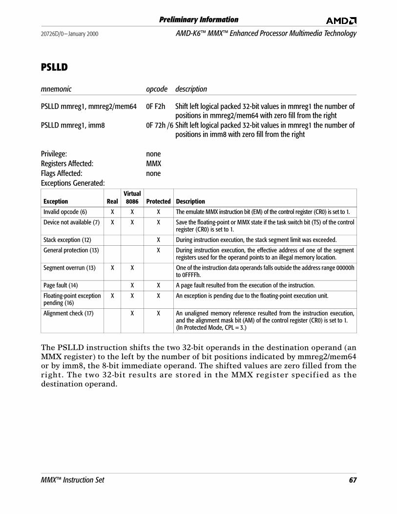
20726D/0—January 2000 AMD-K6™ MMX™ Enhanced Processor Multimedia Technology
Preliminary Information
PSLLD
mnemonic opcode description
PSLLD mmreg1, mmreg2/mem64 0F F2h Shift left logical packed 32-bit values in mmreg1 the number of positions in mmreg2/mem64 with zero fill from the right
PSLLD mmreg1, imm8 0F 72h /6 Shift left logical packed 32-bit values in mmreg1 the number of positions in imm8 with zero fill from the right
Privilege: noneRegisters Affected: MMXFlags Affected: noneExceptions Generated:
The PSLLD instruction shifts the two 32-bit operands in the destination operand (anMMX register) to the left by the number of bit positions indicated by mmreg2/mem64or by imm8, the 8-bit immediate operand. The shifted values are zero filled from theright. The two 32-bit results are stored in the MMX register specified as thedestination operand.
Exception RealVirtual8086 Protected Description
Invalid opcode (6) X X X The emulate MMX instruction bit (EM) of the control register (CR0) is set to 1.
Device not available (7) X X X Save the floating-point or MMX state if the task switch bit (TS) of the controlregister (CR0) is set to 1.
Stack exception (12) X During instruction execution, the stack segment limit was exceeded.
General protection (13) X During instruction execution, the effective address of one of the segmentregisters used for the operand points to an illegal memory location.
Segment overrun (13) X X One of the instruction data operands falls outside the address range 00000hto 0FFFFh.
Page fault (14) X X A page fault resulted from the execution of the instruction.
Floating-point exceptionpending (16)
X X X An exception is pending due to the floating-point execution unit.
Alignment check (17) X X An unaligned memory reference resulted from the instruction execution,and the alignment mask bit (AM) of the control register (CR0) is set to 1.(In Protected Mode, CPL = 3.)
MMX™ Instruction Set 67

AMD-K6™ MMX™ Enhanced Processor Multimedia Technology 20726D/0—January 2000
Preliminary Information
Functional Illustration of the PSLLD Instruction
The following list explains the functional illustration of the PSLLD instruction:
■ The value 0000_0000_0000_0008h in mmreg2/mem64 indicates a shift of 8 bitpositions to the left.
■ The 32-bit value 000F_A3BEh in mmreg1 is shifted 8 bit positions to the left andstored in mmreg1 as 0FA3_BE00h.
■ The 32-bit value 0123_4567h in mmreg1 is shifted 8 bit positions to the left andstored in mmreg1 as 2345_6700h.
Related Instructions See the PSLLQ instruction.
See the PSLLW instruction.
See the PSRAD instruction.
See the PSRAW instruction.
See the PSRLD instruction.
See the PSRLQ instruction.
See the PSRLW instruction.
= =
mmreg2/mem64
mmreg1
mmreg1 2345_6700h0FA3_BE00h
000F_A3BEh
0000_0000_0000_0008h
63 0
63
63
0
0
0123_4567h
68 MMX™ Instruction Set

20726D/0—January 2000 AMD-K6™ MMX™ Enhanced Processor Multimedia Technology
Preliminary Information
PSLLQ
mnemonic opcode description
PSLLQ mmreg1, mmreg2/mem64 0F F3h Shift left logical 64-bit values in mmreg1 the number of positions in mmreg2/mem64 with zero fill from the right
PSLLQ mmreg1, imm8 0F 73h /6 Shift left logical 64-bit values in mmreg1 the number of positions in imm8 with zero fill from the right
Privilege: noneRegisters Affected: MMXFlags Affected: noneExceptions Generated:
The PSLLQ instruction shifts the 64-bit operand in the destination operand (an MMXregister) to the left by the number of bit positions indicated by mmreg2/mem64 or byimm8, the 8-bit immediate operand. The shifted value is zero filled from the right. The64-bit result is stored in the MMX register specified as the destination operand.
Exception RealVirtual8086 Protected Description
Invalid opcode (6) X X X The emulate MMX instruction bit (EM) of the control register (CR0) is set to 1.
Device not available (7) X X X Save the floating-point or MMX state if the task switch bit (TS) of the controlregister (CR0) is set to 1.
Stack exception (12) X During instruction execution, the stack segment limit was exceeded.
General protection (13) X During instruction execution, the effective address of one of the segmentregisters used for the operand points to an illegal memory location.
Segment overrun (13) X X One of the instruction data operands falls outside the address range 00000hto 0FFFFh.
Page fault (14) X X A page fault resulted from the execution of the instruction.
Floating-point exceptionpending (16)
X X X An exception is pending due to the floating-point execution unit.
Alignment check (17) X X An unaligned memory reference resulted from the instruction execution,and the alignment mask bit (AM) of the control register (CR0) is set to 1.(In Protected Mode, CPL = 3.)
MMX™ Instruction Set 69

AMD-K6™ MMX™ Enhanced Processor Multimedia Technology 20726D/0—January 2000
Preliminary Information
Functional Illustration of the PSLLQ Instruction
The following list explains the functional illustration of the PSLLQ instruction:
■ The value 0000_0000_0000_0008h in mmreg2/mem64 indicates a shift of 8 bitpositions to the left.
■ The 64-bit value 000F_A3BE_0123_4567h in mmreg1 is shifted 8 bit positions to theleft and stored in mmreg1 as 0FA3_BE01_2345_6700h.
Related Instructions See the PSLLD instruction.
See the PSLLW instruction.
See the PSRAD instruction.
See the PSRAW instruction.
See the PSRLD instruction.
See the PSRLQ instruction.
See the PSRLW instruction.
=
mmreg2/mem64
mmreg1
mmreg1 0FA3_BE01_2345_6700h
000F_A3BE_0123_4567h
0000_0000_0000_0008h
63 0
63
63
0
0
70 MMX™ Instruction Set

20726D/0—January 2000 AMD-K6™ MMX™ Enhanced Processor Multimedia Technology
Preliminary Information
PSLLW
mnemonic opcode description
PSLLW mmreg1, mmreg2/mem64 0F F1h Shift left logical packed 16-bit values in mmreg1 the number of positions in mmreg2/mem64 with zero fill from the right
PSLLW mmreg1, imm8 0F 71h /6 Shift left logical packed 16-bit values in mmreg1 the number of positions in imm8 with zero fill from the right
Privilege: noneRegisters Affected: MMXFlags Affected: noneExceptions Generated:
The PSLLW instruction shifts the four 16-bit operands in the destination operand (anMMX register) to the left by the number of bit positions indicated by mmreg2/mem64or by imm8, the 8-bit immediate operand. The shifted values are zero filled from theright. The four 16-bit results are stored in the MMX register specified as thedestination operand.
Exception RealVirtual8086 Protected Description
Invalid opcode (6) X X X The emulate MMX instruction bit (EM) of the control register (CR0) is set to 1.
Device not available (7) X X X Save the floating-point or MMX state if the task switch bit (TS) of the controlregister (CR0) is set to 1.
Stack exception (12) X During instruction execution, the stack segment limit was exceeded.
General protection (13) X During instruction execution, the effective address of one of the segmentregisters used for the operand points to an illegal memory location.
Segment overrun (13) X X One of the instruction data operands falls outside the address range 00000hto 0FFFFh.
Page fault (14) X X A page fault resulted from the execution of the instruction.
Floating-point exceptionpending (16)
X X X An exception is pending due to the floating-point execution unit.
Alignment check (17) X X An unaligned memory reference resulted from the instruction execution,and the alignment mask bit (AM) of the control register (CR0) is set to 1.(In Protected Mode, CPL = 3.)
MMX™ Instruction Set 71

AMD-K6™ MMX™ Enhanced Processor Multimedia Technology 20726D/0—January 2000
Preliminary Information
Functional Illustration of the PSLLW Instruction
The following list explains the functional illustration of the PSLLW instruction:
■ The value 0000_0000_0000_0008h in mmreg2/mem64 indicates a shift of 8 bitpositions to the left.
■ The 16-bit value 8807h in mmreg1 is shifted 8 bit positions to the left and stored inmmreg1 as 0700h.
■ The 16-bit value EC22h in mmreg1 is shifted 8 bit positions to the left and stored inmmreg1 as 2200h.
■ The 16-bit value 0FF9h in mmreg1 is shifted 8 bit positions to the left and stored inmmreg1 as F900h.
■ The 16-bit value FFFFh in mmreg1 is shifted 8 bit positions to the left and stored inmmreg1 as FF00h.
Related Instructions See the PSLLD instruction.
See the PSLLQ instruction.
See the PSRAD instruction.
See the PSRAW instruction.
See the PSRLD instruction.
See the PSRLQ instruction.
See the PSRLW instruction.
= = = =
mmreg2/mem64
mmreg1
mmreg1
0000_0000_0000_0008h
FFFFh
FF00h
0FF9h
F900h
EC22h
2200h
8807h
0700h
63
63
63
0
0
0
72 MMX™ Instruction Set

20726D/0—January 2000 AMD-K6™ MMX™ Enhanced Processor Multimedia Technology
Preliminary Information
PSRAD
mnemonic opcode description
PSRAD mmreg1, mmreg2/mem64 0F E2h Shift right arithmetic packed signed 32-bit values in mmreg1 the number of positions in mmreg2/mem64 with sign fill from the left
PSRAD mmreg1, imm8 0F 72h /4 Shift right arithmetic packed signed 32-bit values in mmreg1 the number of positions in imm8 with sign fill from the left
Privilege: noneRegisters Affected: MMXFlags Affected: noneExceptions Generated:
The PSRAD instruction shifts the two signed 32-bit operands in the destinationoperand (an MMX register) to the right by the number of bit positions indicated bymmreg2/mem64 or by imm8, the 8-bit immediate operand. The shifted values are signfilled from the left. The two signed 32-bit results are stored in the MMX registerspecified as the destination operand.
Exception RealVirtual8086 Protected Description
Invalid opcode (6) X X X The emulate MMX instruction bit (EM) of the control register (CR0) is set to 1.
Device not available (7) X X X Save the floating-point or MMX state if the task switch bit (TS) of the controlregister (CR0) is set to 1.
Stack exception (12) X During instruction execution, the stack segment limit was exceeded.
General protection (13) X During instruction execution, the effective address of one of the segmentregisters used for the operand points to an illegal memory location.
Segment overrun (13) X X One of the instruction data operands falls outside the address range 00000hto 0FFFFh.
Page fault (14) X X A page fault resulted from the execution of the instruction.
Floating-point exceptionpending (16)
X X X An exception is pending due to the floating-point execution unit.
Alignment check (17) X X An unaligned memory reference resulted from the instruction execution,and the alignment mask bit (AM) of the control register (CR0) is set to 1.(In Protected Mode, CPL = 3.)
MMX™ Instruction Set 73

AMD-K6™ MMX™ Enhanced Processor Multimedia Technology 20726D/0—January 2000
Preliminary Information
Functional Illustration of the PSRAD Instruction
The following list explains the functional illustration of the PSRAD instruction:
■ The value 0000_0000_0000_0010h in mmreg2/mem64 indicates a shift of 16 bitpositions to the right.
■ The 32-bit negative value FFF0_0000h in mmreg1 is shifted 16 bit positions to theright with sign fill from the left and stored in mmreg1 as FFFF_FFF0h.
■ The 32-bit positive value 0123_0000h in mmreg1 is shifted 16 bit positions to theright with sign fill from the left and stored in mmreg1 as 0000_0123h.
Related Instructions See the PSLLD instruction.
See the PSLLQ instruction.
See the PSLLW instruction.
See the PSRAW instruction.
See the PSRLD instruction.
See the PSRLQ instruction.
See the PSRLW instruction.
See the PUNPCKHWD instruction.
See the PUNPCKLWD instruction.
= =
mmreg2/mem64
mmreg1
mmreg1
0123_0000h
0000_0000_0000_0010h
0000_0123hFFFF_FFF0h
FFF0_0000h
63 0
63
63
0
0
74 MMX™ Instruction Set

20726D/0—January 2000 AMD-K6™ MMX™ Enhanced Processor Multimedia Technology
Preliminary Information
PSRAW
mnemonic opcode description
PSRAW mmreg1, mmreg2/mem64 0F E1h Shift right arithmetic packed signed 16-bit values in mmreg1 the number of positions in mmreg2/mem64 with sign fill from the left
PSRAW mmreg1, imm8 0F 71h /4 Shift right arithmetic packed signed 16-bit values in mmreg1 the number of positions in imm8 with sign fill from the left
Privilege: noneRegisters Affected: MMXFlags Affected: noneExceptions Generated:
The PSRAW instruction shifts the four signed 16-bit operands in the destinationoperand (an MMX register) to the right by the number of bit positions indicated bymmreg2/mem64 or by imm8, the 8-bit immediate operand. The shifted values are signfilled from the left. The four signed 16-bit results are stored in the MMX registerspecified as the destination operand.
Exception RealVirtual8086 Protected Description
Invalid opcode (6) X X X The emulate MMX instruction bit (EM) of the control register (CR0) is set to 1.
Device not available (7) X X X Save the floating-point or MMX state if the task switch bit (TS) of the controlregister (CR0) is set to 1.
Stack exception (12) X During instruction execution, the stack segment limit was exceeded.
General protection (13) X During instruction execution, the effective address of one of the segmentregisters used for the operand points to an illegal memory location.
Segment overrun (13) X X One of the instruction data operands falls outside the address range 00000hto 0FFFFh.
Page fault (14) X X A page fault resulted from the execution of the instruction.
Floating-point exceptionpending (16)
X X X An exception is pending due to the floating-point execution unit.
Alignment check (17) X X An unaligned memory reference resulted from the instruction execution,and the alignment mask bit (AM) of the control register (CR0) is set to 1.(In Protected Mode, CPL = 3.)
MMX™ Instruction Set 75

AMD-K6™ MMX™ Enhanced Processor Multimedia Technology 20726D/0—January 2000
Preliminary Information
Functional Illustration of the PSRAW Instruction
The following list explains the functional illustration of the PSRAW instruction:
■ The value 0000_0000_0000_0008h in mmreg2/mem64 indicates a shift of 8 bitpositions to the right.
■ The 16-bit negative value 8800h in mmreg1 is shifted 8 bit positions to the rightwith sign fill from the left and stored in mmreg1 as FF88h.
■ The 16-bit negative value EC00h in mmreg1 is shifted 8 bit positions to the rightwith sign fill from the left and stored in mmreg1 as FFECh.
■ The 16-bit positive value 0F00h in mmreg1 is shifted 8 bit positions to the rightwith sign fill from the left and stored in mmreg1 as 000Fh.
■ The 16-bit positive value 7F00h in mmreg1 is shifted 8 bit positions to the rightwith sign fill from the left and stored in mmreg1 as 007Fh.
Related Instructions See the PSLLD instruction.
See the PSLLQ instruction.
See the PSLLW instruction.
See the PSRAD instruction.
See the PSRLD instruction.
See the PSRLQ instruction.
See the PSRLW instruction.
See the PUNPCKHBW instruction.
See the PUNPCKLBW instruction.
= = = =
mmreg2/mem64
mmreg1
mmreg1
0000_0000_0000_0008h
7F00h
007Fh
0F00h
000Fh
EC00h
FFECh
8800h
FF88h
63
63
63
0
0
0
76 MMX™ Instruction Set

20726D/0—January 2000 AMD-K6™ MMX™ Enhanced Processor Multimedia Technology
Preliminary Information
PSRLD
mnemonic opcode description
PSRLD mmreg1, mmreg2/mem64 0F D2h Shift right logical packed 32-bit values in mmreg1 the number of positions in mmreg2/mem64 with zero fill from the left
PSRLD mmreg1, imm8 0F 72h /2 Shift right logical packed 32-bit values in mmreg1 the number of positions in imm8 with zero fill from the left
Privilege: noneRegisters Affected: MMXFlags Affected: noneExceptions Generated:
The PSRLD instruction shifts the two 32-bit operands in the destination operand (anMMX register) to the right by the number of bit positions indicated bymmreg2/mem64 or by imm8, the 8-bit immediate operand. The shifted values are zerofilled from the left. The two 32-bit results are stored in the MMX register specified asthe destination operand.
Exception RealVirtual8086 Protected Description
Invalid opcode (6) X X X The emulate MMX instruction bit (EM) of the control register (CR0) is set to 1.
Device not available (7) X X X Save the floating-point or MMX state if the task switch bit (TS) of the controlregister (CR0) is set to 1.
Stack exception (12) X During instruction execution, the stack segment limit was exceeded.
General protection (13) X During instruction execution, the effective address of one of the segmentregisters used for the operand points to an illegal memory location.
Segment overrun (13) X X One of the instruction data operands falls outside the address range 00000hto 0FFFFh.
Page fault (14) X X A page fault resulted from the execution of the instruction.
Floating-point exceptionpending (16)
X X X An exception is pending due to the floating-point execution unit.
Alignment check (17) X X An unaligned memory reference resulted from the instruction execution,and the alignment mask bit (AM) of the control register (CR0) is set to 1.(In Protected Mode, CPL = 3.)
MMX™ Instruction Set 77

AMD-K6™ MMX™ Enhanced Processor Multimedia Technology 20726D/0—January 2000
Preliminary Information
Functional Illustration of the PSRLD Instruction
The following list explains the functional illustration of the PSRLD instruction:
■ The value 0000_0000_0000_0010h in mmreg2/mem64 indicates a shift of 16 bitpositions to the right.
■ The 32-bit value FFF0_0000h in mmreg1 is shifted 16 bit positions to the right andstored in mmreg1 as 0000_FFF0h
■ The 32-bit value 0123_4567h in mmreg1 is shifted 16 bit positions to the right andstored in mmreg1 as 0000_0123h.
Related Instructions See the PSLLD instruction.
See the PSLLQ instruction.
See the PSLLW instruction.
See the PSRAD instruction.
See the PSRAW instruction.
See the PSRLQ instruction.
See the PSRLW instruction.
= =
mmreg2/mem64
mmreg1
mmreg1
0123_4567h
0000_0000_0000_0010h
0000_0123h0000_FFF0h
FFF0_0000h
63 0
63
63
0
0
78 MMX™ Instruction Set

20726D/0—January 2000 AMD-K6™ MMX™ Enhanced Processor Multimedia Technology
Preliminary Information
PSRLQ
mnemonic opcode description
PSRLQ mmreg1, mmreg2/mem64 0F D3h Shift right logical 64-bit values in mmreg1 the number of positions in mmreg2/mem64 with zero fill from the left
PSRLQ mmreg1, imm8 0F 73h /2 Shift right logical 64-bit values in mmreg1 the number of positions in imm8 with zero fill from the left
Privilege: noneRegisters Affected: MMXFlags Affected: noneExceptions Generated:
The PSRLQ instruction shifts the 64-bit operand in the destination operand (an MMXregister) to the right by the number of bit positions indicated by mmreg2/mem64 or byimm8, the 8-bit immediate operand. The shifted value is zero filled from the left. Theresult is stored in the MMX register specified as the destination operand.
Exception RealVirtual8086 Protected Description
Invalid opcode (6) X X X The emulate MMX instruction bit (EM) of the control register (CR0) is set to 1.
Device not available (7) X X X Save the floating-point or MMX state if the task switch bit (TS) of the controlregister (CR0) is set to 1.
Stack exception (12) X During instruction execution, the stack segment limit was exceeded.
General protection (13) X During instruction execution, the effective address of one of the segmentregisters used for the operand points to an illegal memory location.
Segment overrun (13) X X One of the instruction data operands falls outside the address range 00000hto 0FFFFh.
Page fault (14) X X A page fault resulted from the execution of the instruction.
Floating-point exceptionpending (16)
X X X An exception is pending due to the floating-point execution unit.
Alignment check (17) X X An unaligned memory reference resulted from the instruction execution,and the alignment mask bit (AM) of the control register (CR0) is set to 1.(In Protected Mode, CPL = 3.)
MMX™ Instruction Set 79

AMD-K6™ MMX™ Enhanced Processor Multimedia Technology 20726D/0—January 2000
Preliminary Information
Functional Illustration of the PSRLQ Instruction
The following list explains the functional illustration of the PSRLQ instruction:
■ The value 0000_0000_0000_0010h in mmreg2/mem64 indicates a shift of 16 bitpositions to the right.
■ The 64-bit value 000F_A3BE_0123_4567h in mmreg1 is shifted 16 bit positions tothe right and stored in mmreg1 as 0000_000F_A3BE_0123h.
Related Instructions See the PSLLD instruction.
See the PSLLQ instruction.
See the PSLLW instruction.
See the PSRAD instruction.
See the PSRAW instruction.
See the PSRLD instruction.
See the PSRLW instruction.
=
mmreg2/mem64
mmreg1
mmreg1 0000_000F_A3BE_0123h
000F_A3BE_0123_4567h
0000_0000_0000_0010h
63 0
63
63
0
0
80 MMX™ Instruction Set

20726D/0—January 2000 AMD-K6™ MMX™ Enhanced Processor Multimedia Technology
Preliminary Information
PSRLW
mnemonic opcode description
PSRLW mmreg1, mmreg2/mem64 0F D1h Shift right logical packed 16-bit values in mmreg1 the number of positions in mmreg2/mem64 with zero fill from the left
PSRLW mmreg1, imm8 0F 71h /2 Shift right logical packed 16-bit values in mmreg1 the number of positions in imm8 with zero fill from the left
Privilege: noneRegisters Affected: MMXFlags Affected: noneExceptions Generated:
The PSRLW instruction shifts the four 16-bit operands in the destination operand (anMMX register) to the right by the number of bit positions indicated bymmreg2/mem64 or by imm8, the 8-bit immediate operand. The shifted values are zerofilled from the left. The four 16-bit results are stored in the MMX register specified asthe destination operand.
Exception RealVirtual8086 Protected Description
Invalid opcode (6) X X X The emulate MMX instruction bit (EM) of the control register (CR0) is set to 1.
Device not available (7) X X X Save the floating-point or MMX state if the task switch bit (TS) of the controlregister (CR0) is set to 1.
Stack exception (12) X During instruction execution, the stack segment limit was exceeded.
General protection (13) X During instruction execution, the effective address of one of the segmentregisters used for the operand points to an illegal memory location.
Segment overrun (13) X X One of the instruction data operands falls outside the address range 00000hto 0FFFFh.
Page fault (14) X X A page fault resulted from the execution of the instruction.
Floating-point exceptionpending (16)
X X X An exception is pending due to the floating-point execution unit.
Alignment check (17) X X An unaligned memory reference resulted from the instruction execution,and the alignment mask bit (AM) of the control register (CR0) is set to 1.(In Protected Mode, CPL = 3.)
MMX™ Instruction Set 81

AMD-K6™ MMX™ Enhanced Processor Multimedia Technology 20726D/0—January 2000
Preliminary Information
Functional Illustration of the PSRLW Instruction
The following list explains the functional illustration of the PSRLW instruction:
■ The value 0000_0000_0000_0008h in mmreg2/mem64 indicates a shift of 8 bitpositions to the right.
■ The 16-bit value 8800h in mmreg1 is shifted 8 bit positions to the right and storedin mmreg1 as 0088h.
■ The 16-bit value EC22h in mmreg1 is shifted 8 bit positions to the right and storedin mmreg1 as 00ECh.
■ The 16-bit value 0FF9h in mmreg1 is shifted 8 bit positions to the right and storedin mmreg1 as 000Fh.
■ The 16-bit value FF00h in mmreg1 is shifted 8 bit positions to the right and storedin mmreg1 as 00FFh.
Related Instructions See the PSLLD instruction.
See the PSLLQ instruction.
See the PSLLW instruction.
See the PSRAD instruction.
See the PSRAW instruction.
See the PSRLD instruction.
See the PSRLQ instruction.
= = = =
mmreg2/mem64
mmreg1
mmreg1
0000_0000_0000_0008h
FF00h
00FFh
0FF9h
000Fh
EC22h
00ECh
8800h
0088h
63
63
63
0
0
0
82 MMX™ Instruction Set

20726D/0—January 2000 AMD-K6™ MMX™ Enhanced Processor Multimedia Technology
Preliminary Information
PSUBB
mnemonic opcode description
PSUBB mmreg1, mmreg2/mem64 0F F8h Subtract unsigned packed 8-bit values with wraparound
Privilege: noneRegisters Affected: MMXFlags Affected: noneExceptions Generated:
The PSUBB instruction subtracts eight unsigned 8-bit values in the source operand (anMMX register or a 64-bit memory location) from the eight corresponding unsigned8-bit values in the destination operand (an MMX register). If the source operand islarger than the destination operand, the result wraps around.
Exception RealVirtual8086 Protected Description
Invalid opcode (6) X X X The emulate MMX instruction bit (EM) of the control register (CR0) is set to 1.
Device not available (7) X X X Save the floating-point or MMX state if the task switch bit (TS) of the controlregister (CR0) is set to 1.
Stack exception (12) X During instruction execution, the stack segment limit was exceeded.
General protection (13) X During instruction execution, the effective address of one of the segmentregisters used for the operand points to an illegal memory location.
Segment overrun (13) X X One of the instruction data operands falls outside the address range 00000hto 0FFFFh.
Page fault (14) X X A page fault resulted from the execution of the instruction.
Floating-point exceptionpending (16)
X X X An exception is pending due to the floating-point execution unit.
Alignment check (17) X X An unaligned memory reference resulted from the instruction execution,and the alignment mask bit (AM) of the control register (CR0) is set to 1.(In Protected Mode, CPL = 3.)
MMX™ Instruction Set 83

AMD-K6™ MMX™ Enhanced Processor Multimedia Technology 20726D/0—January 2000
Preliminary Information
Functional Illustration of the PSUBB Instruction
The following list explains the functional illustration of the PSUBB instruction:
■ The unsigned 8-bit value ECh is subtracted from the unsigned 8-bit value 53h andwraps around to 67h.
■ The unsigned 8-bit value F7h is subtracted from the unsigned 8-bit value 07h andwraps around to 10h.
■ The unsigned 8-bit value A8h is subtracted from the unsigned 8-bit value 9Ah andwraps around to F2h.
■ All the remaining operations are simple subtraction with no wraparound.
Related Instructions See the PSUBD instruction.
See the PSUBW instruction.
See the PSUBSB instruction.
See the PSUBSW instruction.
See the PSUBUSB instruction.
See the PSUBUSW instruction.
− − − − − − −−
= = = = = = ==
mmreg2/mem64
mmreg1
mmreg1
00h
00h
00h
9Ah
A8h
F2h
70h 07h
F7h
10h
44h
2Ch
77h
14h
63h
42h
00h
42h
53h
ECh
67h
D2h
88h
4Ah
63
63
63
0
0
0
84 MMX™ Instruction Set

20726D/0—January 2000 AMD-K6™ MMX™ Enhanced Processor Multimedia Technology
Preliminary Information
PSUBD
mnemonic opcode description
PSUBD mmreg1, mmreg2/mem64 0F FAh Subtract unsigned packed 32-bit values with wraparound
Privilege: noneRegisters Affected: MMXFlags Affected: noneExceptions Generated:
The PSUBD instruction subtracts two unsigned 32-bit values in the source operand (anMMX register or a 64-bit memory location) from the two corresponding unsigned32-bit values in the destination operand (an MMX register). If the source operand islarger than the destination operand, the result wraps around.
Exception RealVirtual8086 Protected Description
Invalid opcode (6) X X X The emulate MMX instruction bit (EM) of the control register (CR0) is set to 1.
Device not available (7) X X X Save the floating-point or MMX state if the task switch bit (TS) of the controlregister (CR0) is set to 1.
Stack exception (12) X During instruction execution, the stack segment limit was exceeded.
General protection (13) X During instruction execution, the effective address of one of the segmentregisters used for the operand points to an illegal memory location.
Segment overrun (13) X X One of the instruction data operands falls outside the address range 00000hto 0FFFFh.
Page fault (14) X X A page fault resulted from the execution of the instruction.
Floating-point exceptionpending (16)
X X X An exception is pending due to the floating-point execution unit.
Alignment check (17) X X An unaligned memory reference resulted from the instruction execution,and the alignment mask bit (AM) of the control register (CR0) is set to 1.(In Protected Mode, CPL = 3.)
MMX™ Instruction Set 85

AMD-K6™ MMX™ Enhanced Processor Multimedia Technology 20726D/0—January 2000
Preliminary Information
Functional Illustration of the PSUBD Instruction
The following list explains the functional illustration of the PSUBD instruction:
■ The unsigned 32-bit value 8000_0000h is subtracted from the unsigned 32-bit value0123_4567h and wraps around to 8123_4567h.
■ The remaining operation is a simple subtraction with no wraparound.
Related Instructions See the PSUBB instruction.
See the PSUBW instruction.
See the PSUBSB instruction.
See the PSUBSW instruction.
See the PSUBUSB instruction.
See the PSUBUSW instruction.
− −
= =
mmreg2/mem64
mmreg1
mmreg1
0123_4567h
8000_0000h
8123_4567hFFE0_B885h
000F_A3BEh
FFF0_5C43h
63 0
63
63
0
0
86 MMX™ Instruction Set

20726D/0—January 2000 AMD-K6™ MMX™ Enhanced Processor Multimedia Technology
Preliminary Information
PSUBSB
mnemonic opcode description
PSUBSB mmreg1, mmreg2/mem64 0F E8h Subtract signed packed 8-bit values and saturate
Privilege: noneRegisters Affected: MMXFlags Affected: noneExceptions Generated:
The PSUBSB instruction subtracts eight signed 8-bit values in the source operand (anMMX register or a 64-bit memory location) from the eight corresponding signed 8-bitvalues in the destination operand (an MMX register). If a result is less than –128 (80h),it saturates to –128 (80h). If a result is greater than 127 (7Fh), it saturates to 127 (7Fh).The eight signed 8-bit results are stored in the MMX register specified as thedestination operand.
Exception RealVirtual8086 Protected Description
Invalid opcode (6) X X X The emulate MMX instruction bit (EM) of the control register (CR0) is set to 1.
Device not available (7) X X X Save the floating-point or MMX state if the task switch bit (TS) of the controlregister (CR0) is set to 1.
Stack exception (12) X During instruction execution, the stack segment limit was exceeded.
General protection (13) X During instruction execution, the effective address of one of the segmentregisters used for the operand points to an illegal memory location.
Segment overrun (13) X X One of the instruction data operands falls outside the address range 00000hto 0FFFFh.
Page fault (14) X X A page fault resulted from the execution of the instruction.
Floating-point exceptionpending (16)
X X X An exception is pending due to the floating-point execution unit.
Alignment check (17) X X An unaligned memory reference resulted from the instruction execution,and the alignment mask bit (AM) of the control register (CR0) is set to 1.(In Protected Mode, CPL = 3.)
MMX™ Instruction Set 87

AMD-K6™ MMX™ Enhanced Processor Multimedia Technology 20726D/0—January 2000
Preliminary Information
Functional Illustration of the PSUBSB Instruction
The following list explains the functional illustration of the PSUBSB instruction:
■ The signed 8-bit positive value 0Fh is subtracted from the signed 8-bit negativevalue 82h, and the result saturates to 80h because it is less than 80h, the smallestpossible signed 8-bit value.
■ The signed 8-bit negative value C1h is subtracted from the signed 8-bit positivevalue 42h, and the result saturates to 7Fh because it is greater than 7Fh, thelargest possible signed 8-bit value.
■ All the remaining operations are simple signed subtraction with no saturation.
Related Instructions See the PSUBB instruction.
See the PSUBD instruction.
See the PSUBW instruction.
See the PSUBSW instruction.
See the PSUBUSB instruction.
See the PSUBUSW instruction.
− − − − − − −−
= = = = = = ==
mmreg2/mem64
mmreg1
mmreg1
82h
0Fh
80h
9Ah
A8h
F2h
70h 07h
F7h
10h
44h
2Ch
77h
14h
63h
42h
C1h
7Fh
53h
ECh
67h
D2h
88h
4Ah
63
63
63
0
0
0
Indicates a saturated value
88 MMX™ Instruction Set

20726D/0—January 2000 AMD-K6™ MMX™ Enhanced Processor Multimedia Technology
Preliminary Information
PSUBSW
mnemonic opcode description
PSUBSW mmreg1, mmreg2/mem64 0F E9h Subtract signed packed 16-bit values and saturate
Privilege: noneRegisters Affected: MMXFlags Affected: noneExceptions Generated:
The PSUBSW instruction subtracts four signed 16-bit values in the source operand (anMMX register or a 64-bit memory location) from the four corresponding signed 16-bitvalues in the destination operand (an MMX register). If a result is less than –32768(8000h), it saturates to –32768 (8000h). If a result is greater than 32767 (7FFFh), itsaturates to 32767 (7FFFh). The four signed 16-bit results are stored in the MMXregister specified as the destination operand.
Exception RealVirtual8086 Protected Description
Invalid opcode (6) X X X The emulate MMX instruction bit (EM) of the control register (CR0) is set to 1.
Device not available (7) X X X Save the floating-point or MMX state if the task switch bit (TS) of the controlregister (CR0) is set to 1.
Stack exception (12) X During instruction execution, the stack segment limit was exceeded.
General protection (13) X During instruction execution, the effective address of one of the segmentregisters used for the operand points to an illegal memory location.
Segment overrun (13) X X One of the instruction data operands falls outside the address range 00000hto 0FFFFh.
Page fault (14) X X A page fault resulted from the execution of the instruction.
Floating-point exceptionpending (16)
X X X An exception is pending due to the floating-point execution unit.
Alignment check (17) X X An unaligned memory reference resulted from the instruction execution,and the alignment mask bit (AM) of the control register (CR0) is set to 1.(In Protected Mode, CPL = 3.)
MMX™ Instruction Set 89

AMD-K6™ MMX™ Enhanced Processor Multimedia Technology 20726D/0—January 2000
Preliminary Information
Functional Illustration of the PSUBSW Instruction
The following list explains the functional illustration of the PSUBSW instruction:
■ The signed 16-bit negative value D320h is subtracted from the signed 16-bitpositive value 5321h, and the result saturates to 7FFFh because it is greater than7FFFh, the largest possible signed 16-bit value.
■ The signed 16-bit positive value 0FF9h is subtracted from the signed 16-bitnegative value 8007h, and the result saturates to 8000h because it is less than8000h, the smallest possible signed 16-bit value.
■ The remaining operations are simple signed subtraction with no saturation.
Related Instructions See the PSUBB instruction.
See the PSUBD instruction.
See the PSUBW instruction.
See the PSUBSB instruction.
See the PSUBUSB instruction.
See the PSUBUSW instruction.
− − − −
= = = =
mmreg2/mem64
mmreg1
mmreg1
FFFFhD250h
FFFFh
0000h
8007h
0FF9h
8000h
5321h
D320h
7FFFh
8807h
4A49h
63
63
63
0
0
0
Indicates a saturated value
90 MMX™ Instruction Set

20726D/0—January 2000 AMD-K6™ MMX™ Enhanced Processor Multimedia Technology
Preliminary Information
PSUBUSB
mnemonic opcode description
PSUBUSB mmreg1, mmreg2/mem64 0F D8h Subtract unsigned packed 8-bit values and saturate
Privilege: noneRegisters Affected: MMXFlags Affected: noneExceptions Generated:
The PSUBUSB instruction subtracts eight unsigned 8-bit values in the source operand(an MMX register or a 64-bit memory location) from the eight corresponding unsigned8-bit values in the destination operand (an MMX register). If any 8-bit source value isgreater than its corresponding 8-bit destination value, the result saturates to 00h. Theeight unsigned 8-bit results are stored in the MMX register specified as thedestination operand.
Exception RealVirtual8086 Protected Description
Invalid opcode (6) X X X The emulate MMX instruction bit (EM) of the control register (CR0) is set to 1.
Device not available (7) X X X Save the floating-point or MMX state if the task switch bit (TS) of the controlregister (CR0) is set to 1.
Stack exception (12) X During instruction execution, the stack segment limit was exceeded.
General protection (13) X During instruction execution, the effective address of one of the segmentregisters used for the operand points to an illegal memory location.
Segment overrun (13) X X One of the instruction data operands falls outside the address range 00000hto 0FFFFh.
Page fault (14) X X A page fault resulted from the execution of the instruction.
Floating-point exceptionpending (16)
X X X An exception is pending due to the floating-point execution unit.
Alignment check (17) X X An unaligned memory reference resulted from the instruction execution,and the alignment mask bit (AM) of the control register (CR0) is set to 1.(In Protected Mode, CPL = 3.)
MMX™ Instruction Set 91

AMD-K6™ MMX™ Enhanced Processor Multimedia Technology 20726D/0—January 2000
Preliminary Information
Functional Illustration of the PSUBUSB Instruction
The following list explains the functional illustration of the PSUBUSB instruction:
■ The unsigned 8-bit value ECh is subtracted from the unsigned 8-bit value 53h, andthe result saturates to 00h because the source operand is greater than thedestination operand.
■ The unsigned 8-bit value C1h is subtracted from the unsigned 8-bit value 42h, andthe result saturates to 00h because the source operand is greater than thedestination operand.
■ The unsigned 8-bit value F7h is subtracted from the unsigned 8-bit value 07h, andthe result saturates to 00h because the source operand is greater than thedestination operand.
■ All the remaining operations are simple unsigned subtraction with no saturation.
Related Instructions See the PSUBB instruction.
See the PSUBD instruction.
See the PSUBW instruction.
See the PSUBSB instruction.
See the PSUBSW instruction.
See the PSUBUSW instruction.
− − − − − − −−
= = = = = = ==
mmreg2/mem64
mmreg1
mmreg1
82h
0Fh
73h
9Ah
98h
02h
70h 07h
F7h
00h
44h
2Ch
77h
14h
63h
42h
C1h
00h
53h
ECh
00h
D2h
88h
4Ah
63
63
63
0
0
0
Indicates a saturated value
92 MMX™ Instruction Set

20726D/0—January 2000 AMD-K6™ MMX™ Enhanced Processor Multimedia Technology
Preliminary Information
PSUBUSW
mnemonic opcode description
PSUBUSW mmreg1, mmreg2/mem64 0F D9h Subtract unsigned packed 16-bit values and saturate
Privilege: noneRegisters Affected: MMXFlags Affected: noneExceptions Generated:
The PSUBUSW instruction subtracts four unsigned 16-bit values in the sourceoperand (an MMX register or a 64-bit memory location) from the four correspondingunsigned 16-bit values in the destination operand (an MMX register). If any 16-bitsource value is greater than its corresponding 16-bit destination value, the resultsaturates to 0000h. The four unsigned 16-bit results are stored in the MMX registerspecified as the destination operand.
Exception RealVirtual8086 Protected Description
Invalid opcode (6) X X X The emulate MMX instruction bit (EM) of the control register (CR0) is set to 1.
Device not available (7) X X X Save the floating-point or MMX state if the task switch bit (TS) of the controlregister (CR0) is set to 1.
Stack exception (12) X During instruction execution, the stack segment limit was exceeded.
General protection (13) X During instruction execution, the effective address of one of the segmentregisters used for the operand points to an illegal memory location.
Segment overrun (13) X X One of the instruction data operands falls outside the address range 00000hto 0FFFFh.
Page fault (14) X X A page fault resulted from the execution of the instruction.
Floating-point exceptionpending (16)
X X X An exception is pending due to the floating-point execution unit.
Alignment check (17) X X An unaligned memory reference resulted from the instruction execution,and the alignment mask bit (AM) of the control register (CR0) is set to 1.(In Protected Mode, CPL = 3.)
MMX™ Instruction Set 93

AMD-K6™ MMX™ Enhanced Processor Multimedia Technology 20726D/0—January 2000
Preliminary Information
Functional Illustration of the PSUBUSW Instruction
The following list explains the functional illustration of the PSUBUSW instruction:
■ The unsigned 16-bit value EC22h is subtracted from the unsigned 16-bit value5321h, and the result saturates to 0000h because the source operand is greaterthan the destination operand.
■ The remaining operations are simple unsigned subtraction with no saturation.
Related Instructions See the PSUBB instruction.
See the PSUBD instruction.
See the PSUBW instruction.
See the PSUBSB instruction.
See the PSUBSW instruction.
See the PSUBUSB instruction.
− − − −
= = = =
mmreg2/mem64
mmreg1
mmreg1
FFFFhD250h
FFFFh
0000h
7007h
0FF9h
600Eh
5321h
EC22h
0000h
8807h
4A49h
63
63
63
0
0
0
Indicates a saturated value
94 MMX™ Instruction Set

20726D/0—January 2000 AMD-K6™ MMX™ Enhanced Processor Multimedia Technology
Preliminary Information
PSUBW
mnemonic opcode description
PSUBW mmreg1, mmreg2/mem64 0F F9h Subtract unsigned packed 16-bit values with wraparound
Privilege: noneRegisters Affected: MMXFlags Affected: noneExceptions Generated:
The PSUBW instruction subtracts four unsigned 16-bit values in the source operand(an MMX register or a 64-bit memory location) from the four corresponding unsigned16-bit values in the destination operand (an MMX register). If the source operand islarger than the destination operand, the result wraps around.
Exception RealVirtual8086 Protected Description
Invalid opcode (6) X X X The emulate MMX instruction bit (EM) of the control register (CR0) is set to 1.
Device not available (7) X X X Save the floating-point or MMX state if the task switch bit (TS) of the controlregister (CR0) is set to 1.
Stack exception (12) X During instruction execution, the stack segment limit was exceeded.
General protection (13) X During instruction execution, the effective address of one of the segmentregisters used for the operand points to an illegal memory location.
Segment overrun (13) X X One of the instruction data operands falls outside the address range 00000hto 0FFFFh.
Page fault (14) X X A page fault resulted from the execution of the instruction.
Floating-point exceptionpending (16)
X X X An exception is pending due to the floating-point execution unit.
Alignment check (17) X X An unaligned memory reference resulted from the instruction execution,and the alignment mask bit (AM) of the control register (CR0) is set to 1.(In Protected Mode, CPL = 3.)
MMX™ Instruction Set 95

AMD-K6™ MMX™ Enhanced Processor Multimedia Technology 20726D/0—January 2000
Preliminary Information
Functional Illustration of the PSUBW Instruction
The following list explains the functional illustration of the PSUBW instruction:
■ The unsigned 16-bit value EC22h is subtracted from the unsigned 16-bit value5321h and the result wraps around to 66FFh.
■ The remaining operations are simple unsigned subtraction with no saturation.
Related Instructions See the PSUBB instruction.
See the PSUBD instruction.
See the PSUBSB instruction.
See the PSUBSW instruction.
See the PSUBUSB instruction.
See the PSUBUSW instruction.
− − − −
= = = =
mmreg2/mem64
mmreg1
mmreg1
FFFFhD250h
FFFFh
0000h
7007h
0FF9h
600Eh
5321h
EC22h
66FFh
8807h
4A49h
63
63
63
0
0
0
96 MMX™ Instruction Set

20726D/0—January 2000 AMD-K6™ MMX™ Enhanced Processor Multimedia Technology
Preliminary Information
PUNPCKHBW
mnemonic opcode description
PUNPCKHBW mmreg1, mmreg2/mem64 0F 68h Unpack the high 32 bits of packed 8-bit values
Privilege: noneRegisters Affected: MMXFlags Affected: noneExceptions Generated:
The PUNPCKHBW instruction unpacks and interleaves four 8-bit values from the high32 bits of the source operand (an MMX register or a 64-bit memory location) and four8-bit values from the high 32 bits of the destination operand (an MMX register). The8-bit values from the source operand become the high 8 bits of the 16-bit results, andthe 8-bit values from the destination operand become the low 8 bits of the 16-bitresults. The eight interleaved 8-bit values are stored in the MMX register specified asthe destination operand.
Exception RealVirtual8086 Protected Description
Invalid opcode (6) X X X The emulate MMX instruction bit (EM) of the control register (CR0) is set to 1.
Device not available (7) X X X Save the floating-point or MMX state if the task switch bit (TS) of the controlregister (CR0) is set to 1.
Stack exception (12) X During instruction execution, the stack segment limit was exceeded.
General protection (13) X During instruction execution, the effective address of one of the segmentregisters used for the operand points to an illegal memory location.
Segment overrun (13) X X One of the instruction data operands falls outside the address range 00000hto 0FFFFh.
Page fault (14) X X A page fault resulted from the execution of the instruction.
Floating-point exceptionpending (16)
X X X An exception is pending due to the floating-point execution unit.
Alignment check (17) X X An unaligned memory reference resulted from the instruction execution,and the alignment mask bit (AM) of the control register (CR0) is set to 1.(In Protected Mode, CPL = 3.)
MMX™ Instruction Set 97

AMD-K6™ MMX™ Enhanced Processor Multimedia Technology 20726D/0—January 2000
Preliminary Information
Functional Illustration of the PUNPCKHBW Instruction
In the following figure, the destination register is shown at the center to illustrate theflow of data from the two source operands.
In the functional illustration of the PUNPCKHBW instruction, the 8-bit values frommmreg1 are stored in the low-order 8 bits of the 16-bit result. The mmreg2/mem64source operand is set to all zero bits so it can provide zero fill in the high-order 8 bits ofthe 16-bit result. This is a method that can be used to expand unsigned 8-bit valuesinto unsigned 16-bit operands for subsequent processing that requires higherprecision.
Related Instructions See the PACKSSWB instruction.
See the PACKUSWB instruction.
See the PSRAW instruction.
See the PUNPCKHDQ instruction.
See the PUNPCKHWD instruction.
See the PUNPCKLBW instruction.
See the PUNPCKLDQ instruction.
See the PUNPCKLWD instruction.
source mmreg2/mem64
destination mmreg1
source mmreg1
00h
00h
88h
00h
A8h
80h
00h 00h
00h
FEh
44h
06h
00h
00h
7Fh
00h
80h
A8h
00h
00h
44h
00h
88h
80h
63
63
63
0
0
98 MMX™ Instruction Set

20726D/0—January 2000 AMD-K6™ MMX™ Enhanced Processor Multimedia Technology
Preliminary Information
PUNPCKHDQ
mnemonic opcode description
PUNPCKHDQ mmreg1, mmreg2/mem64 0F 6Ah Unpack the high 32 bits of packed 32-bit values
Privilege: noneRegisters Affected: MMXFlags Affected: noneExceptions Generated:
The PUNPCKHDQ instruction unpacks and interleaves the high 32 bits of the sourceoperand (an MMX register or a 64-bit memory location) and the high 32 bits of thedestination operand (an MMX register). The 32-bit value from the source operandbecomes the high 32 bits of the 64-bit result, and the 32-bit value from the destinationoperand becomes the low 32 bits of the 64-bit result. The interleaved 32-bit values arestored in the MMX register specified as the destination operand.
Exception RealVirtual8086 Protected Description
Invalid opcode (6) X X X The emulate MMX instruction bit (EM) of the control register (CR0) is set to 1.
Device not available (7) X X X Save the floating-point or MMX state if the task switch bit (TS) of the controlregister (CR0) is set to 1.
Stack exception (12) X During instruction execution, the stack segment limit was exceeded.
General protection (13) X During instruction execution, the effective address of one of the segmentregisters used for the operand points to an illegal memory location.
Segment overrun (13) X X One of the instruction data operands falls outside the address range 00000hto 0FFFFh.
Page fault (14) X X A page fault resulted from the execution of the instruction.
Floating-point exceptionpending (16)
X X X An exception is pending due to the floating-point execution unit.
Alignment check (17) X X An unaligned memory reference resulted from the instruction execution,and the alignment mask bit (AM) of the control register (CR0) is set to 1.(In Protected Mode, CPL = 3.)
MMX™ Instruction Set 99

AMD-K6™ MMX™ Enhanced Processor Multimedia Technology 20726D/0—January 2000
Preliminary Information
Functional Illustration of the PUNPCKHDQ Instruction
In the following figure, the destination register is shown at the center to illustrate theflow of data from the two source operands.
In the functional illustration of the PUNPCKHDQ instruction, the 32-bit value frommmreg1 is stored in the low-order 32 bits of the 64-bit result. The mmreg2/mem64source operand is set to all zero bits so it can provide zero fill in the high-order 32 bitsof the 64-bit result. This is a method that can be used to expand unsigned 32-bit valuesinto unsigned 64-bit operands for subsequent processing that requires higherprecision.
Related Instructions See the PUNPCKHBW instruction.
See the PUNPCKHWD instruction.
See the PUNPCKLBW instruction.
See the PUNPCKLDQ instruction.
See the PUNPCKLWD instruction.
source mmreg2/mem64
destination mmreg1
source mmreg1
0000_0000h
0000_0000h
8880_44A8h
0000_0000h
8880_44A8h
7F06_FE80h
63
63 0
0
100 MMX™ Instruction Set

20726D/0—January 2000 AMD-K6™ MMX™ Enhanced Processor Multimedia Technology
Preliminary Information
PUNPCKHWD
mnemonic opcode description
PUNPCKHWD mmreg1, mmreg2/mem64 0F 69h Unpack the high 32 bits of packed 16-bit values
Privilege: noneRegisters Affected: MMXFlags Affected: noneExceptions Generated:
The PUNPCKHWD instruction unpacks and interleaves two 16-bit values from thehigh 32 bits of the source operand (an MMX register or a 64-bit memory location) andtwo 16-bit values from the high 32 bits of the destination operand (an MMX register).The 16-bit values from the source operand become the high 16 bits of the 32-bitresults, and the 16-bit values from the destination operand become the low 16 bits ofthe 32-bit results. The four interleaved 16-bit values are stored in the MMX registerspecified as the destination operand.
Exception RealVirtual8086 Protected Description
Invalid opcode (6) X X X The emulate MMX instruction bit (EM) of the control register (CR0) is set to 1.
Device not available (7) X X X Save the floating-point or MMX state if the task switch bit (TS) of the controlregister (CR0) is set to 1.
Stack exception (12) X During instruction execution, the stack segment limit was exceeded.
General protection (13) X During instruction execution, the effective address of one of the segmentregisters used for the operand points to an illegal memory location.
Segment overrun (13) X X One of the instruction data operands falls outside the address range 00000hto 0FFFFh.
Page fault (14) X X A page fault resulted from the execution of the instruction.
Floating-point exceptionpending (16)
X X X An exception is pending due to the floating-point execution unit.
Alignment check (17) X X An unaligned memory reference resulted from the instruction execution,and the alignment mask bit (AM) of the control register (CR0) is set to 1.(In Protected Mode, CPL = 3.)
MMX™ Instruction Set 101

AMD-K6™ MMX™ Enhanced Processor Multimedia Technology 20726D/0—January 2000
Preliminary Information
Functional Illustration of the PUNPCKHWD Instruction
In the following figure, the destination register is shown at the center to illustrate theflow of data from the two source operands.
In the functional illustration of the PUNPCKHWD instruction, the 16-bit values frommmreg1 are stored in the low-order 16 bits of the 32-bit result. The 16-bit values fromthe mmreg2/mem64 source operand are stored in the high-order 16 bits of the 32-bitresult. This is an example of the use of the PUNPCKHWD instruction to assemble32-bit operands from the high and low 16-bit results produced by the PMULHW andPMULLW instructions. In this example, the high and low 16-bit results are interleavedto produce the signed 32-bit results 1569_4030h and F98C_7662h.
Related Instructions See the PACKSSDW instruction.
See the PSRAD instruction.
See the PMULHW instruction.
See the PMULLW instruction.
See the PUNPCKHBW instruction.
See the PUNPCKHDQ instruction.
See the PUNPCKLBW instruction.
See the PUNPCKLDQ instruction.
See the PUNPCKLWD instruction.
source mmreg2/mem64
destination mmreg1
source mmreg1
1569h
1569h
4030h
0000h
7662h
0001h
06FDh
F98Ch
5FCFh
F98Ch
4030h
7662h
63
63 0
0
102 MMX™ Instruction Set

20726D/0—January 2000 AMD-K6™ MMX™ Enhanced Processor Multimedia Technology
Preliminary Information
PUNPCKLBW
mnemonic opcode description
PUNPCKLBW mmreg1, mmreg2/mem32 0F 60h Unpack the low 32-bits of packed 8-bit values
Privilege: noneRegisters Affected: MMXFlags Affected: noneExceptions Generated:
The PUNPCKLBW instruction unpacks and interleaves four 8-bit values from the low32 bits of the source operand (an MMX register or a 32-bit memory location) and four8-bit values from the low 32 bits of the destination operand (an MMX register). The8-bit values from the source operand become the high 8 bits of the 16-bit results, andthe 8-bit values from the destination operand become the low 8 bits of the 16-bitresults. The eight interleaved 8-bit values are stored in the MMX register specified asthe destination operand.
Exception RealVirtual8086 Protected Description
Invalid opcode (6) X X X The emulate MMX instruction bit (EM) of the control register (CR0) is set to 1.
Device not available (7) X X X Save the floating-point or MMX state if the task switch bit (TS) of the controlregister (CR0) is set to 1.
Stack exception (12) X During instruction execution, the stack segment limit was exceeded.
General protection (13) X During instruction execution, the effective address of one of the segmentregisters used for the operand points to an illegal memory location.
Segment overrun (13) X X One of the instruction data operands falls outside the address range 00000hto 0FFFFh.
Page fault (14) X X A page fault resulted from the execution of the instruction.
Floating-point exceptionpending (16)
X X X An exception is pending due to the floating-point execution unit.
Alignment check (17) X X An unaligned memory reference resulted from the instruction execution,and the alignment mask bit (AM) of the control register (CR0) is set to 1.(In Protected Mode, CPL = 3.)
MMX™ Instruction Set 103

AMD-K6™ MMX™ Enhanced Processor Multimedia Technology 20726D/0—January 2000
Preliminary Information
Functional Illustration of the PUNPCKLBW Instruction
In the following figure, the destination register is shown at the center to illustrate theflow of data from the two source operands.
In the functional illustration of the PUNPCKLBW instruction, the 8-bit values frommmreg1 are stored in the low-order 8 bits of the 16-bit result. The mmreg2/mem32source operand is set to all zero bits so it can provide zero fill in the high-order 8 bits ofthe 16-bit result. This is a method that can be used to expand unsigned 8-bit values
source mmreg2
destination mmreg1
source mmreg1
00h
00h
88h
00h
80h
80h
00h 00h
00h
FEh
FEh
06h
00h
00h
7Fh
00h
06h
A8h
00h
00h
44h
00h
7Fh
80h
63
63 0
0
00h00h 00h00h
0
source mem32
destination mmreg1
source mmreg1
00h 80h00hFEh00h06h00h7Fh
31
88h 80hFEh06h7FhA8h44h80h
63 0
104 MMX™ Instruction Set

20726D/0—January 2000 AMD-K6™ MMX™ Enhanced Processor Multimedia Technology
Preliminary Information
into unsigned 16-bit operands for subsequent processing that requires higherprecision.
Related Instructions See the PACKSSWB instruction.
See the PACKUSWB instruction.
See the PSRAW instruction.
See the PUNPCKHBW instruction
See the PUNPCKHDQ instruction.
See the PUNPCKHWD instruction.
See the PUNPCKLDQ instruction.
See the PUNPCKLWD instruction.
MMX™ Instruction Set 105

AMD-K6™ MMX™ Enhanced Processor Multimedia Technology 20726D/0—January 2000
Preliminary Information
PUNPCKLDQ
mnemonic opcode description
PUNPCKLDQ mmreg1, mmreg2/mem32 0F 62h Unpack the low 32 bits of packed 32-bit values
Privilege: noneRegisters Affected: MMXFlags Affected: noneExceptions Generated:
The PUNPCKLDQ instruction unpacks and interleaves the low 32 bits of the sourceoperand (an MMX register or a 32-bit memory location) and the low 32 bits of thedestination operand (an MMX register). The 32-bit value from the source operandbecomes the high 32 bits of the 64-bit result, and the 32-bit value from the destinationoperand becomes the low 32 bits of the 64-bit result. The interleaved 32-bit values arestored in the MMX register specified as the destination operand.
Exception RealVirtual8086 Protected Description
Invalid opcode (6) X X X The emulate MMX instruction bit (EM) of the control register (CR0) is set to 1.
Device not available (7) X X X Save the floating-point or MMX state if the task switch bit (TS) of the controlregister (CR0) is set to 1.
Stack exception (12) X During instruction execution, the stack segment limit was exceeded.
General protection (13) X During instruction execution, the effective address of one of the segmentregisters used for the operand points to an illegal memory location.
Segment overrun (13) X X One of the instruction data operands falls outside the address range 00000hto 0FFFFh.
Page fault (14) X X A page fault resulted from the execution of the instruction.
Floating-point exceptionpending (16)
X X X An exception is pending due to the floating-point execution unit.
Alignment check (17) X X An unaligned memory reference resulted from the instruction execution,and the alignment mask bit (AM) of the control register (CR0) is set to 1.(In Protected Mode, CPL = 3.)
106 MMX™ Instruction Set

20726D/0—January 2000 AMD-K6™ MMX™ Enhanced Processor Multimedia Technology
Preliminary Information
Functional Illustration of the PUNPCKLDQ Instruction
In the following figure, the destination register is shown at the center to illustrate theflow of data from the two source operands.
In the functional illustration of the PUNPCKLDQ instruction, the 32-bit value frommmreg1 is stored in the low-order 32 bits of the 64-bit result. The mmreg2/mem32source operand is set to all zero bits so it can provide zero fill in the high-order 32 bitsof the 64-bit result. This is a method that can be used to expand unsigned 32-bit valuesinto unsigned 64-bit operands for subsequent processing that requires higherprecision.
source mmreg2
destination mmreg1
source mmreg1
0000_0000h
0000_0000h
8880_44A8h
0000_0000h
7F06_FE80h
7F06_FE80h
63
63 0
0
source mem32
destination mmreg1
source mmreg1
0000_0000h
0000_0000h
7F06_FE80h
31 0
8880_44A8h 7F06_FE80h
63 0
MMX™ Instruction Set 107

AMD-K6™ MMX™ Enhanced Processor Multimedia Technology 20726D/0—January 2000
Preliminary Information
Related Instructions See the PUNPCKHBW instruction.
See the PUNPCKHDQ instruction.
See the PUNPCKHWD instruction.
See the PUNPCKLBW instruction.
See the PUNPCKLWD instruction.
108 MMX™ Instruction Set

20726D/0—January 2000 AMD-K6™ MMX™ Enhanced Processor Multimedia Technology
Preliminary Information
PUNPCKLWD
mnemonic opcode description
PUNPCKLWD mmreg1, mmreg2/mem32 0F 61h Unpack the low 32 bits of packed 16-bit values
Privilege: noneRegisters Affected: MMXFlags Affected: noneExceptions Generated:
The PUNPCKLWD instruction unpacks and interleaves two 16-bit values from the low32 bits of the source operand (an MMX register or a 32-bit memory location) and two16-bit values from the low 32 bits of the destination operand (an MMX register). The16-bit values from the source operand become the high 16 bits of the 32-bit results,and the 16-bit values from the destination operand become the low 16 bits of the 32-bitresults. The four interleaved 16-bit values are stored in the MMX register specified asthe destination operand.
Exception RealVirtual8086 Protected Description
Invalid opcode (6) X X X The emulate MMX instruction bit (EM) of the control register (CR0) is set to 1.
Device not available (7) X X X Save the floating-point or MMX state if the task switch bit (TS) of the controlregister (CR0) is set to 1.
Stack exception (12) X During instruction execution, the stack segment limit was exceeded.
General protection (13) X During instruction execution, the effective address of one of the segmentregisters used for the operand points to an illegal memory location.
Segment overrun (13) X X One of the instruction data operands falls outside the address range 00000hto 0FFFFh.
Page fault (14) X X A page fault resulted from the execution of the instruction.
Floating-point exceptionpending (16)
X X X An exception is pending due to the floating-point execution unit.
Alignment check (17) X X An unaligned memory reference resulted from the instruction execution,and the alignment mask bit (AM) of the control register (CR0) is set to 1.(In Protected Mode, CPL = 3.)
MMX™ Instruction Set 109

AMD-K6™ MMX™ Enhanced Processor Multimedia Technology 20726D/0—January 2000
Preliminary Information
Functional Illustration of the PUNPCKLWD Instruction
In the following figure, the destination register is shown at the center to illustrate theflow of data from the two source operands.
In the functional illustration of the PUNPCKLWD instruction, the 16-bit values frommmreg1 are stored in the low-order 16 bits of the 32-bit result. The 16-bit values fromthe mmreg2/mem32 source operand are stored in the high-order 16 bits of the 32-bitresult. This is an example of the use of the PUNPCKLWD instruction to assemble32-bit operands from the high and low 16-bit results produced by the PMULHW andPMULLW instructions. In this example, the high and low 16-bit results are interleavedto produce the signed 32-bit results 06FD_5FCFh and 0000_0001h.
source mmreg2
destination mmreg1
source mmreg1
1569h
06FDh
4030h
0000h
0001h
0001h
06FDh
0000h
5FCFh
F98Ch
5FCFh
7662h
63
63 0
0
0000h06FDh
0
source mem32
destination mmreg1
source mmreg1
06FDh 0001h0000h5FCFh
31
31
4030h 0001h5FCFh7662h
63 0
110 MMX™ Instruction Set

20726D/0—January 2000 AMD-K6™ MMX™ Enhanced Processor Multimedia Technology
Preliminary Information
Related Instructions See the PACKSSWD instruction.
See the PSRAD instruction.
See the PMULHW instruction.
See the PMULLW instruction.
See the PUNPCKHBW instruction.
See the PUNPCKHDQ instruction.
See the PUNPCKHWD instruction.
See the PUNPCKLBW instruction.
See the PUNPCKLDQ instruction.
MMX™ Instruction Set 111

AMD-K6™ MMX™ Enhanced Processor Multimedia Technology 20726D/0—January 2000
Preliminary Information
PXOR
mnemonic opcode description
PXOR mmreg1, mmreg2/mem64 0F EFh XOR 64-bit values
Privilege: noneRegisters Affected: MMXFlags Affected: noneExceptions Generated:
The PXOR instruction logically XORs the 64 bits of the source operand (an MMXregister or a 64-bit memory location) with the 64 bits of the destination operand (anMMX register) and stores the result in the destination register.
A logical XOR produces a 1 bit if only one of the two input bits is a 1. If both input bitsare 0 or both input bits are 1, a logical XOR produces a 0 bit.
Exception RealVirtual8086 Protected Description
Invalid opcode (6) X X X The emulate MMX instruction bit (EM) of the control register (CR0) is set to 1.
Device not available (7) X X X Save the floating-point or MMX state if the task switch bit (TS) of the controlregister (CR0) is set to 1.
Stack exception (12) X During instruction execution, the stack segment limit was exceeded.
General protection (13) X During instruction execution, the effective address of one of the segmentregisters used for the operand points to an illegal memory location.
Segment overrun (13) X X One of the instruction data operands falls outside the address range 00000hto 0FFFFh.
Page fault (14) X X A page fault resulted from the execution of the instruction.
Floating-point exceptionpending (16)
X X X An exception is pending due to the floating-point execution unit.
Alignment check (17) X X An unaligned memory reference resulted from the instruction execution,and the alignment mask bit (AM) of the control register (CR0) is set to 1.(In Protected Mode, CPL = 3.)
112 MMX™ Instruction Set

20726D/0—January 2000 AMD-K6™ MMX™ Enhanced Processor Multimedia Technology
Preliminary Information
Functional Illustration of the PXOR Instruction
In the functional illustration of the PXOR instruction, the 64-bit source value islogically XOR’d to the 64-bit destination value, and the result is stored in thedestination register.
Related Instructions See the PAND instruction.
See the PANDN instruction.
See the POR instruction.
0101_1100_1100_0011 1100_1101_0100_1110 1011_0001_0011_1001 0110_0011_0101_1001
1111_0011_1100_1110 1100_0010_0100_0001 0111_0000_0000_1000 1110_1111_1000_1000
mmreg1
032 3163 4748 1516
032 3163 4748 1516
mmreg2/mem64
Logical OR Logical OR Logical OR Logical OR
mmreg1
032 3163 4748 1516
Result
1010_1111_0000_1101 0000_1111_0000_1111 1100_0001_0011_0001 1000_1100_1101_0011
MMX™ Instruction Set 113

AMD-K6™ MMX™ Enhanced Processor Multimedia Technology 20726D/0—January 2000
Preliminary Information
114 MMX™ Instruction Set