Embed Size (px)
Citation preview

Preliminary Information
AMD-K6-2
Processor
Data Sheet
®

© 2000 Advanced Micro Devices, Inc. All rights reserved.
The contents of this document are provided in connection with Advanced Micro
Devices, Inc. ("AMD") products. AMD makes no representations or warranties with
respect to the accuracy or completeness of the contents of this publication and
reserves the right to make changes to specifications and product descriptions at any
time without notice. No license, whether express, implied, arising by estoppel or
otherwise, to any intellectual property rights is granted by this publication. Except
as set forth in AMD’s Standard Terms and Conditions of Sale, AMD assumes no
liability whatsoever, and disclaims any express or implied warranty, relating to its
products including, but not limited to, the implied warranty of merchantability,
fitness for a particular purpose, or infringement of any intellectual property right.
AMD’s products are not designed, intended, authorized or warranted for use as
components in systems intended for surgical implant into the body, or in other
applications intended to support or sustain life, or in any other application in which
the failure of AMD’s product could create a situation where personal injury, death,
or severe property or environmental damage may occur. AMD reserves the right to
discontinue or make changes to its products at any time without notice.
Trademarks
AMD, the AMD logo, K6, 3DNow!, and combinations thereof, K86, and Super7 are trademarks, and AMD-K6
and RISC86 are registered trademarks of Advanced Micro Devices, Inc.
Microsoft, Windows, and Windows NT are registered trademarks of Microsoft Corporation.
NetWare is a registered trademark of Novell, Inc.
MMX is a trademark of Intel Corporation.
The TAP State Diagram is reprinted from IEEE Std 1149.1-1990 “IEEE Standard Test Access Port and Bound-
ary-Scan Architecture,” Copyright © 1990 by the Institute of Electrical and Electronics Engineers, Inc. The
IEEE disclaims any responsibility or liability resulting from the placement and use in the described manner.
Information is reprinted with the permission of the IEEE.
Other product names used in this publication are for identification purposes only and may be trademarks of
their respective companies.

Contents iii
21850J/0—February 2000 AMD-K6®-2 Processor Data Sheet
Preliminary Information
Contents
Revision Historyxix
1 AMD-K6®-2 Processor . . . . . . . . . . . . . . . . . . . . . . . . . . . . . . . . . 1
1.1 Super7™ Platform Initiative . . . . . . . . . . . . . . . . . . . . . . . . . . . 3
Super7™ Platform Enhancements. . . . . . . . . . . . . . . . . . . . . . . 3
Super7™ Platform Advantages . . . . . . . . . . . . . . . . . . . . . . . . . 4
2 Internal Architecture . . . . . . . . . . . . . . . . . . . . . . . . . . . . . . . . . 5
2.1 Introduction . . . . . . . . . . . . . . . . . . . . . . . . . . . . . . . . . . . . . . . . 5
2.2 AMD-K6®-2 Processor Microarchitecture Overview . . . . . . . . 5
Enhanced RISC86® Microarchitecture . . . . . . . . . . . . . . . . . . . 6
2.3 Cache, Instruction Prefetch, and Predecode Bits . . . . . . . . . . 9
Cache . . . . . . . . . . . . . . . . . . . . . . . . . . . . . . . . . . . . . . . . . . . . . . 9
Prefetching. . . . . . . . . . . . . . . . . . . . . . . . . . . . . . . . . . . . . . . . . 10
Predecode Bits . . . . . . . . . . . . . . . . . . . . . . . . . . . . . . . . . . . . . . 10
2.4 Instruction Fetch and Decode . . . . . . . . . . . . . . . . . . . . . . . . . 11
Instruction Fetch . . . . . . . . . . . . . . . . . . . . . . . . . . . . . . . . . . . . 11
Instruction Decode . . . . . . . . . . . . . . . . . . . . . . . . . . . . . . . . . . 12
2.5 Centralized Scheduler . . . . . . . . . . . . . . . . . . . . . . . . . . . . . . . 14
2.6 Execution Units . . . . . . . . . . . . . . . . . . . . . . . . . . . . . . . . . . . . 15
Register X and Y Pipelines . . . . . . . . . . . . . . . . . . . . . . . . . . . 16
2.7 Branch-Prediction Logic . . . . . . . . . . . . . . . . . . . . . . . . . . . . . 17
Branch History Table. . . . . . . . . . . . . . . . . . . . . . . . . . . . . . . . . 18
Branch Target Cache . . . . . . . . . . . . . . . . . . . . . . . . . . . . . . . . . 18
Return Address Stack . . . . . . . . . . . . . . . . . . . . . . . . . . . . . . . . 18
Branch Execution Unit . . . . . . . . . . . . . . . . . . . . . . . . . . . . . . . 19
3 Software Environment . . . . . . . . . . . . . . . . . . . . . . . . . . . . . . . 21
3.1 Registers . . . . . . . . . . . . . . . . . . . . . . . . . . . . . . . . . . . . . . . . . . 21
General-Purpose Registers . . . . . . . . . . . . . . . . . . . . . . . . . . . . 22
Integer Data Types . . . . . . . . . . . . . . . . . . . . . . . . . . . . . . . . . . 23
Segment Registers. . . . . . . . . . . . . . . . . . . . . . . . . . . . . . . . . . . 24
Segment Usage . . . . . . . . . . . . . . . . . . . . . . . . . . . . . . . . . . . . . 24
Instruction Pointer . . . . . . . . . . . . . . . . . . . . . . . . . . . . . . . . . . 25
Floating-Point Registers . . . . . . . . . . . . . . . . . . . . . . . . . . . . . . 25
Floating-Point Register Data Types. . . . . . . . . . . . . . . . . . . . . 28
MMX™/3DNow!™ Registers. . . . . . . . . . . . . . . . . . . . . . . . . . . 29
MMX™ Data Types . . . . . . . . . . . . . . . . . . . . . . . . . . . . . . . . . . 29
3DNow!™ Data Types . . . . . . . . . . . . . . . . . . . . . . . . . . . . . . . . 30
EFLAGS Register . . . . . . . . . . . . . . . . . . . . . . . . . . . . . . . . . . . 31
Control Registers. . . . . . . . . . . . . . . . . . . . . . . . . . . . . . . . . . . . 32
Debug Registers. . . . . . . . . . . . . . . . . . . . . . . . . . . . . . . . . . . . . 34
Model-Specific Registers (MSR) . . . . . . . . . . . . . . . . . . . . . . . 37

iv Contents
AMD-K6®-2 Processor Data Sheet 21850J/0—February 2000
Preliminary Information
Memory Management Registers . . . . . . . . . . . . . . . . . . . . . . . 40
Task State Segment . . . . . . . . . . . . . . . . . . . . . . . . . . . . . . . . . . 42
Paging . . . . . . . . . . . . . . . . . . . . . . . . . . . . . . . . . . . . . . . . . . . . . 43
Descriptors and Gates . . . . . . . . . . . . . . . . . . . . . . . . . . . . . . . . 46
Exceptions and Interrupts . . . . . . . . . . . . . . . . . . . . . . . . . . . . 49
3.2 AMD-K6®-2 Processor Model 8/[F:8] Registers . . . . . . . . . . . 50
Extended Feature Enable Register (EFER)–Model 8/[F:8] . 50
Write Handling Control Register (WHCR)–Model 8/[F:8] . . 51
UC/WC Cacheability Control Register
(UWCCR)52
Processor State Observability Register (PSOR). . . . . . . . . . . 53
Page Flush/Invalidate Register (PFIR) . . . . . . . . . . . . . . . . . . 53
3.3 Instructions Supported by the AMD-K6®-2 Processor . . . . . 54
4 Signal Descriptions . . . . . . . . . . . . . . . . . . . . . . . . . . . . . . . . . . 83
4.1 Signal Terminology . . . . . . . . . . . . . . . . . . . . . . . . . . . . . . . . . 83
4.2 A20M# (Address Bit 20 Mask) . . . . . . . . . . . . . . . . . . . . . . . . . 85
4.3 A[31:3] (Address Bus) . . . . . . . . . . . . . . . . . . . . . . . . . . . . . . . 86
4.4 ADS# (Address Strobe) . . . . . . . . . . . . . . . . . . . . . . . . . . . . . . 87
4.5 ADSC# (Address Strobe Copy) . . . . . . . . . . . . . . . . . . . . . . . . 87
4.6 AHOLD (Address Hold) . . . . . . . . . . . . . . . . . . . . . . . . . . . . . . 88
4.7 AP (Address Parity) . . . . . . . . . . . . . . . . . . . . . . . . . . . . . . . . . 89
4.8 APCHK# (Address Parity Check) . . . . . . . . . . . . . . . . . . . . . . 90
4.9 BE[7:0]# (Byte Enables) . . . . . . . . . . . . . . . . . . . . . . . . . . . . . . 91
4.10 BF[2:0] (Bus Frequency) . . . . . . . . . . . . . . . . . . . . . . . . . . . . . 92
4.11 BOFF# (Backoff) . . . . . . . . . . . . . . . . . . . . . . . . . . . . . . . . . . . . 93
4.12 BRDY# (Burst Ready) . . . . . . . . . . . . . . . . . . . . . . . . . . . . . . . 94
4.13 BRDYC# (Burst Ready Copy) . . . . . . . . . . . . . . . . . . . . . . . . . 95
4.14 BREQ (Bus Request) . . . . . . . . . . . . . . . . . . . . . . . . . . . . . . . . 96
4.15 CACHE# (Cacheable Access) . . . . . . . . . . . . . . . . . . . . . . . . . 96
4.16 CLK (Clock) . . . . . . . . . . . . . . . . . . . . . . . . . . . . . . . . . . . . . . . 97
4.17 D/C# (Data/Code) . . . . . . . . . . . . . . . . . . . . . . . . . . . . . . . . . . . 97
4.18 D[63:0] (Data Bus) . . . . . . . . . . . . . . . . . . . . . . . . . . . . . . . . . . 98
4.19 DP[7:0] (Data Parity) . . . . . . . . . . . . . . . . . . . . . . . . . . . . . . . . 99
4.20 EADS# (External Address Strobe) . . . . . . . . . . . . . . . . . . . . 100
4.21 EWBE# (External Write Buffer Empty) . . . . . . . . . . . . . . . . 101
4.22 FERR# (Floating-Point Error) . . . . . . . . . . . . . . . . . . . . . . . 102
4.23 FLUSH# (Cache Flush) . . . . . . . . . . . . . . . . . . . . . . . . . . . . . 103
4.24 HIT# (Inquire Cycle Hit) . . . . . . . . . . . . . . . . . . . . . . . . . . . . 104
4.25 HITM# (Inquire Cycle Hit To Modified Line) . . . . . . . . . . . 104
4.26 HLDA (Hold Acknowledge) . . . . . . . . . . . . . . . . . . . . . . . . . 105
4.27 HOLD (Bus Hold Request) . . . . . . . . . . . . . . . . . . . . . . . . . . 105
4.28 IGNNE# (Ignore Numeric Exception) . . . . . . . . . . . . . . . . . 106
4.29 INIT (Initialization) . . . . . . . . . . . . . . . . . . . . . . . . . . . . . . . . 107
4.30 INTR (Maskable Interrupt) . . . . . . . . . . . . . . . . . . . . . . . . . . 108
4.31 INV (Invalidation Request) . . . . . . . . . . . . . . . . . . . . . . . . . . 108
4.32 KEN# (Cache Enable) . . . . . . . . . . . . . . . . . . . . . . . . . . . . . . 109

Contents v
21850J/0—February 2000 AMD-K6®-2 Processor Data Sheet
Preliminary Information
4.33 LOCK# (Bus Lock) . . . . . . . . . . . . . . . . . . . . . . . . . . . . . . . . . 110
4.34 M/IO# (Memory or I/O) . . . . . . . . . . . . . . . . . . . . . . . . . . . . . 111
4.35 NA# (Next Address) . . . . . . . . . . . . . . . . . . . . . . . . . . . . . . . . 112
4.36 NMI (Non-Maskable Interrupt) . . . . . . . . . . . . . . . . . . . . . . . 112
4.37 PCD (Page Cache Disable) . . . . . . . . . . . . . . . . . . . . . . . . . . 113
4.38 PCHK# (Parity Check) . . . . . . . . . . . . . . . . . . . . . . . . . . . . . . 114
4.39 PWT (Page Writethrough) . . . . . . . . . . . . . . . . . . . . . . . . . . . 115
4.40 RESET (Reset) . . . . . . . . . . . . . . . . . . . . . . . . . . . . . . . . . . . . 116
4.41 RSVD (Reserved) . . . . . . . . . . . . . . . . . . . . . . . . . . . . . . . . . . 116
4.42 SCYC (Split Cycle) . . . . . . . . . . . . . . . . . . . . . . . . . . . . . . . . . 117
4.43 SMI# (System Management Interrupt) . . . . . . . . . . . . . . . . 117
4.44 SMIACT# (System Management Interrupt Active) . . . . . . 118
4.45 STPCLK# (Stop Clock) . . . . . . . . . . . . . . . . . . . . . . . . . . . . . . 119
4.46 TCK (Test Clock) . . . . . . . . . . . . . . . . . . . . . . . . . . . . . . . . . . 119
4.47 TDI (Test Data Input) . . . . . . . . . . . . . . . . . . . . . . . . . . . . . . 120
4.48 TDO (Test Data Output) . . . . . . . . . . . . . . . . . . . . . . . . . . . . 120
4.49 TMS (Test Mode Select) . . . . . . . . . . . . . . . . . . . . . . . . . . . . 120
4.50 TRST# (Test Reset) . . . . . . . . . . . . . . . . . . . . . . . . . . . . . . . . 121
4.51 VCC2DET (VCC2 Detect) . . . . . . . . . . . . . . . . . . . . . . . . . . . . 121
4.52 VCC2H/L# (VCC2 High/Low) . . . . . . . . . . . . . . . . . . . . . . . . . 121
4.53 W/R# (Write/Read) . . . . . . . . . . . . . . . . . . . . . . . . . . . . . . . . . 122
4.54 WB/WT# (Writeback or Writethrough) . . . . . . . . . . . . . . . . 123
5 Bus Cycles . . . . . . . . . . . . . . . . . . . . . . . . . . . . . . . . . . . . . . . . 127
5.1 Timing Diagrams . . . . . . . . . . . . . . . . . . . . . . . . . . . . . . . . . . 127
5.2 Bus State Machine Diagram . . . . . . . . . . . . . . . . . . . . . . . . . 129
Idle . . . . . . . . . . . . . . . . . . . . . . . . . . . . . . . . . . . . . . . . . . . . . . 130
Address . . . . . . . . . . . . . . . . . . . . . . . . . . . . . . . . . . . . . . . . . . . 130
Data. . . . . . . . . . . . . . . . . . . . . . . . . . . . . . . . . . . . . . . . . . . . . . 130
Data-NA# Requested. . . . . . . . . . . . . . . . . . . . . . . . . . . . . . . . 130
Pipeline Address . . . . . . . . . . . . . . . . . . . . . . . . . . . . . . . . . . . 130
Pipeline Data . . . . . . . . . . . . . . . . . . . . . . . . . . . . . . . . . . . . . . 131
Transition . . . . . . . . . . . . . . . . . . . . . . . . . . . . . . . . . . . . . . . . . 131
5.3 Memory Reads and Writes . . . . . . . . . . . . . . . . . . . . . . . . . . 132
Single-Transfer Memory Read and Write . . . . . . . . . . . . . . . 132
Misaligned Single-Transfer Memory Read and Write . . . . . 134
Burst Reads and Pipelined Burst Reads . . . . . . . . . . . . . . . . 136
Burst Writeback. . . . . . . . . . . . . . . . . . . . . . . . . . . . . . . . . . . . 138
5.4 I/O Read and Write . . . . . . . . . . . . . . . . . . . . . . . . . . . . . . . . 140
Basic I/O Read and Write . . . . . . . . . . . . . . . . . . . . . . . . . . . . 140
Misaligned I/O Read and Write . . . . . . . . . . . . . . . . . . . . . . . 141
5.5 Inquire and Bus Arbitration Cycles . . . . . . . . . . . . . . . . . . . 142
Hold and Hold Acknowledge Cycle . . . . . . . . . . . . . . . . . . . . 142
HOLD-Initiated Inquire Hit to Shared or Exclusive Line . . 144
HOLD-Initiated Inquire Hit to Modified Line . . . . . . . . . . . 146
AHOLD-Initiated Inquire Miss. . . . . . . . . . . . . . . . . . . . . . . . 148
AHOLD-Initiated Inquire Hit to Shared or Exclusive Line. 150
vi Contents
AMD-K6®-2 Processor Data Sheet 21850J/0—February 2000
Preliminary Information
AHOLD-Initiated Inquire Hit to Modified Line . . . . . . . . . . 152
AHOLD Restriction. . . . . . . . . . . . . . . . . . . . . . . . . . . . . . . . . 154
Bus Backoff (BOFF#). . . . . . . . . . . . . . . . . . . . . . . . . . . . . . . . 156
Locked Cycles . . . . . . . . . . . . . . . . . . . . . . . . . . . . . . . . . . . . . 158
Basic Locked Operation . . . . . . . . . . . . . . . . . . . . . . . . . . . . . 158
Locked Operation with BOFF# Intervention . . . . . . . . . . . . 160
Interrupt Acknowledge. . . . . . . . . . . . . . . . . . . . . . . . . . . . . . 162
5.6 Special Bus Cycles . . . . . . . . . . . . . . . . . . . . . . . . . . . . . . . . . 164
Basic Special Bus Cycle . . . . . . . . . . . . . . . . . . . . . . . . . . . . . 164
Shutdown Cycle . . . . . . . . . . . . . . . . . . . . . . . . . . . . . . . . . . . . 166
Stop Grant and Stop Clock States . . . . . . . . . . . . . . . . . . . . . 167
INIT-Initiated Transition from Protected Mode to
Real Mode . . . . . . . . . . . . . . . . . . . . . . . . . . . . . . . . . . . . . . . . 170
6 Power-on Configuration and Initialization . . . . . . . . . . . . . . 173
6.1 Signals Sampled During the Falling Transition of RESET 173
FLUSH# . . . . . . . . . . . . . . . . . . . . . . . . . . . . . . . . . . . . . . . . . . 173
BF[2:0] . . . . . . . . . . . . . . . . . . . . . . . . . . . . . . . . . . . . . . . . . . . 173
BRDYC# . . . . . . . . . . . . . . . . . . . . . . . . . . . . . . . . . . . . . . . . . . 173
6.2 RESET Requirements . . . . . . . . . . . . . . . . . . . . . . . . . . . . . . 174
6.3 State of Processor After RESET . . . . . . . . . . . . . . . . . . . . . . 174
Output Signals . . . . . . . . . . . . . . . . . . . . . . . . . . . . . . . . . . . . . 174
Registers. . . . . . . . . . . . . . . . . . . . . . . . . . . . . . . . . . . . . . . . . . 174
6.4 State of Processor After INIT . . . . . . . . . . . . . . . . . . . . . . . . 177
7 Cache Organization . . . . . . . . . . . . . . . . . . . . . . . . . . . . . . . . . 179
7.1 MESI States in the Data Cache . . . . . . . . . . . . . . . . . . . . . . . 180
7.2 Predecode Bits . . . . . . . . . . . . . . . . . . . . . . . . . . . . . . . . . . . . 180
7.3 Cache Operation . . . . . . . . . . . . . . . . . . . . . . . . . . . . . . . . . . . 181
Cache-Related Signals . . . . . . . . . . . . . . . . . . . . . . . . . . . . . . 183
7.4 Cache Disabling and Flushing . . . . . . . . . . . . . . . . . . . . . . . 183
7.5 Cache-Line Fills . . . . . . . . . . . . . . . . . . . . . . . . . . . . . . . . . . . 184
7.6 Cache-Line Replacements . . . . . . . . . . . . . . . . . . . . . . . . . . . 185
7.7 Write Allocate . . . . . . . . . . . . . . . . . . . . . . . . . . . . . . . . . . . . . 186
Write to a Cacheable Page . . . . . . . . . . . . . . . . . . . . . . . . . . . 186
Write to a Sector . . . . . . . . . . . . . . . . . . . . . . . . . . . . . . . . . . . 187
Write Allocate Limit . . . . . . . . . . . . . . . . . . . . . . . . . . . . . . . . 187
Write Allocate Logic Mechanisms and Conditions . . . . . . . 189
7.8 Prefetching . . . . . . . . . . . . . . . . . . . . . . . . . . . . . . . . . . . . . . . 192
Hardware Prefetching . . . . . . . . . . . . . . . . . . . . . . . . . . . . . . . 192
Software Prefetching. . . . . . . . . . . . . . . . . . . . . . . . . . . . . . . . 192
7.9 Cache States . . . . . . . . . . . . . . . . . . . . . . . . . . . . . . . . . . . . . . 192
7.10 Cache Coherency . . . . . . . . . . . . . . . . . . . . . . . . . . . . . . . . . . 194
Inquire Cycles . . . . . . . . . . . . . . . . . . . . . . . . . . . . . . . . . . . . . 194
Internal Snooping . . . . . . . . . . . . . . . . . . . . . . . . . . . . . . . . . . 194
FLUSH# . . . . . . . . . . . . . . . . . . . . . . . . . . . . . . . . . . . . . . . . . . 195
PFIR . . . . . . . . . . . . . . . . . . . . . . . . . . . . . . . . . . . . . . . . . . . . . 195
Contents vii
21850J/0—February 2000 AMD-K6®-2 Processor Data Sheet
Preliminary Information
WBINVD and INVD. . . . . . . . . . . . . . . . . . . . . . . . . . . . . . . . . 196
Cache-Line Replacement . . . . . . . . . . . . . . . . . . . . . . . . . . . . 196
Cache Snooping . . . . . . . . . . . . . . . . . . . . . . . . . . . . . . . . . . . . 198
7.11 Writethrough versus Writeback Coherency States . . . . . . . 199
7.12 A20M# Masking of Cache Accesses . . . . . . . . . . . . . . . . . . . 199
8 Write Merge Buffer . . . . . . . . . . . . . . . . . . . . . . . . . . . . . . . . . 201
8.1 EWBE Control . . . . . . . . . . . . . . . . . . . . . . . . . . . . . . . . . . . . . 201
8.2 Memory Type Range Registers . . . . . . . . . . . . . . . . . . . . . . . 203
UC/WC Cacheability Control Register (UWCCR) . . . . . . . . 203
9 Floating-Point and Multimedia Execution Units . . . . . . . . . 207
9.1 Floating-Point Execution Unit . . . . . . . . . . . . . . . . . . . . . . . 207
Handling Floating-Point Exceptions . . . . . . . . . . . . . . . . . . . 207
External Logic Support of Floating-Point Exceptions . . . . . 207
9.2 Multimedia and 3DNow!™ Execution Units . . . . . . . . . . . . 209
9.3 Floating-Point and MMX™/3DNow!™ Instruction Compatibili-
ty 209
Registers. . . . . . . . . . . . . . . . . . . . . . . . . . . . . . . . . . . . . . . . . . 209
Exceptions . . . . . . . . . . . . . . . . . . . . . . . . . . . . . . . . . . . . . . . . 209
FERR# and IGNNE# . . . . . . . . . . . . . . . . . . . . . . . . . . . . . . . . 209
10 System Management Mode (SMM) . . . . . . . . . . . . . . . . . . . . 211
10.1 Overview . . . . . . . . . . . . . . . . . . . . . . . . . . . . . . . . . . . . . . . . . 211
10.2 SMM Operating Mode and Default Register Values . . . . . 211
10.3 SMM State-Save Area . . . . . . . . . . . . . . . . . . . . . . . . . . . . . . 214
10.4 SMM Revision Identifier . . . . . . . . . . . . . . . . . . . . . . . . . . . . 216
10.5 SMM Base Address . . . . . . . . . . . . . . . . . . . . . . . . . . . . . . . . . 217
10.6 Halt Restart Slot . . . . . . . . . . . . . . . . . . . . . . . . . . . . . . . . . . . 217
10.7 I/O Trap Dword . . . . . . . . . . . . . . . . . . . . . . . . . . . . . . . . . . . . 218
10.8 I/O Trap Restart Slot . . . . . . . . . . . . . . . . . . . . . . . . . . . . . . . 219
10.9 Exceptions, Interrupts, and Debug in SMM . . . . . . . . . . . . 220
11 Test and Debug . . . . . . . . . . . . . . . . . . . . . . . . . . . . . . . . . . . . 221
11.1 Built-In Self-Test (BIST) . . . . . . . . . . . . . . . . . . . . . . . . . . . . 221
11.2 Tri-State Test Mode . . . . . . . . . . . . . . . . . . . . . . . . . . . . . . . . 222
11.3 Boundary-Scan Test Access Port (TAP) . . . . . . . . . . . . . . . . 223
Test Access Port . . . . . . . . . . . . . . . . . . . . . . . . . . . . . . . . . . . . 223
TAP Signals . . . . . . . . . . . . . . . . . . . . . . . . . . . . . . . . . . . . . . . 223
TAP Registers . . . . . . . . . . . . . . . . . . . . . . . . . . . . . . . . . . . . . 224
TAP Instructions . . . . . . . . . . . . . . . . . . . . . . . . . . . . . . . . . . . 231
TAP Controller State Machine . . . . . . . . . . . . . . . . . . . . . . . . 232
11.4 L1 Cache Inhibit . . . . . . . . . . . . . . . . . . . . . . . . . . . . . . . . . . . 235
Purpose . . . . . . . . . . . . . . . . . . . . . . . . . . . . . . . . . . . . . . . . . . . 235
11.5 Debug . . . . . . . . . . . . . . . . . . . . . . . . . . . . . . . . . . . . . . . . . . . . 236
Debug Registers. . . . . . . . . . . . . . . . . . . . . . . . . . . . . . . . . . . . 236
Debug Exceptions . . . . . . . . . . . . . . . . . . . . . . . . . . . . . . . . . . 241

viii Contents
AMD-K6®-2 Processor Data Sheet 21850J/0—February 2000
Preliminary Information
12 Clock Control . . . . . . . . . . . . . . . . . . . . . . . . . . . . . . . . . . . . . . 243
12.1 Halt State . . . . . . . . . . . . . . . . . . . . . . . . . . . . . . . . . . . . . . . . 244
Enter Halt State . . . . . . . . . . . . . . . . . . . . . . . . . . . . . . . . . . . 244
Exit Halt State . . . . . . . . . . . . . . . . . . . . . . . . . . . . . . . . . . . . . 244
12.2 Stop Grant State . . . . . . . . . . . . . . . . . . . . . . . . . . . . . . . . . . . 245
Enter Stop Grant State . . . . . . . . . . . . . . . . . . . . . . . . . . . . . . 245
Exit Stop Grant State . . . . . . . . . . . . . . . . . . . . . . . . . . . . . . . 245
12.3 Stop Grant Inquire State . . . . . . . . . . . . . . . . . . . . . . . . . . . . 246
Enter Stop Grant Inquire State . . . . . . . . . . . . . . . . . . . . . . . 246
Exit Stop Grant Inquire State . . . . . . . . . . . . . . . . . . . . . . . . 246
12.4 Stop Clock State . . . . . . . . . . . . . . . . . . . . . . . . . . . . . . . . . . . 246
Enter Stop Clock State . . . . . . . . . . . . . . . . . . . . . . . . . . . . . . 246
Exit Stop Clock State . . . . . . . . . . . . . . . . . . . . . . . . . . . . . . . 247
13 Power and Grounding . . . . . . . . . . . . . . . . . . . . . . . . . . . . . . . 249
13.1 Power Connections . . . . . . . . . . . . . . . . . . . . . . . . . . . . . . . . . 249
13.2 Decoupling Recommendations . . . . . . . . . . . . . . . . . . . . . . . 250
13.3 Pin Connection Requirements . . . . . . . . . . . . . . . . . . . . . . . 251
14 Electrical Data . . . . . . . . . . . . . . . . . . . . . . . . . . . . . . . . . . . . . 253
14.1 Electrical Data for OPN Suffixes AHX, 400AFQ, and AFR 253
Operating Ranges . . . . . . . . . . . . . . . . . . . . . . . . . . . . . . . . . . 253
Absolute Ratings . . . . . . . . . . . . . . . . . . . . . . . . . . . . . . . . . . . 254
DC Characteristics. . . . . . . . . . . . . . . . . . . . . . . . . . . . . . . . . . 254
Power Dissipation . . . . . . . . . . . . . . . . . . . . . . . . . . . . . . . . . . 257
14.2 Electrical Data for OPN Suffixes AGR, AFX, and 400AFR 258
Operating Ranges . . . . . . . . . . . . . . . . . . . . . . . . . . . . . . . . . . 258
Absolute Ratings . . . . . . . . . . . . . . . . . . . . . . . . . . . . . . . . . . . 259
DC Characteristics. . . . . . . . . . . . . . . . . . . . . . . . . . . . . . . . . . 259
Power Dissipation . . . . . . . . . . . . . . . . . . . . . . . . . . . . . . . . . . 262
15 I/O Buffer Characteristics . . . . . . . . . . . . . . . . . . . . . . . . . . . 263
15.1 Selectable Drive Strength . . . . . . . . . . . . . . . . . . . . . . . . . . . 263
15.2 I/O Buffer Model . . . . . . . . . . . . . . . . . . . . . . . . . . . . . . . . . . . 264
15.3 I/O Model Application Note . . . . . . . . . . . . . . . . . . . . . . . . . 265
15.4 I/O Buffer AC and DC Characteristics . . . . . . . . . . . . . . . . . 265
16 Signal Switching Characteristics . . . . . . . . . . . . . . . . . . . . . . 267
16.1 CLK Switching Characteristics . . . . . . . . . . . . . . . . . . . . . . . 267
16.2 Clock Switching Characteristics for 100-MHz Bus
Operation . . . . . . . . . . . . . . . . . . . . . . . . . . . . . . . . . . . . . . . . 268
16.3 Clock Switching Characteristics for 66-MHz Bus
Operation . . . . . . . . . . . . . . . . . . . . . . . . . . . . . . . . . . . . . . . . 268
16.4 Valid Delay, Float, Setup, and Hold Timings . . . . . . . . . . . 269

Contents ix
21850J/0—February 2000 AMD-K6®-2 Processor Data Sheet
Preliminary Information
16.5 Output Delay Timings for 100-MHz Bus Operation . . . . . . 270
16.6 Input Setup and Hold Timings for 100-MHz Bus
Operation . . . . . . . . . . . . . . . . . . . . . . . . . . . . . . . . . . . . . . . . 272
16.7 Output Delay Timings for 66-MHz Bus Operation . . . . . . . 274
16.8 Input Setup and Hold Timings for 66-MHz Bus Operation 276
16.9 RESET and Test Signal Timing . . . . . . . . . . . . . . . . . . . . . . 278
17 Thermal Design . . . . . . . . . . . . . . . . . . . . . . . . . . . . . . . . . . . . 285
17.1 Package Thermal Specifications . . . . . . . . . . . . . . . . . . . . . . 285
Heat Dissipation Path . . . . . . . . . . . . . . . . . . . . . . . . . . . . . . . 290
Measuring Case Temperature . . . . . . . . . . . . . . . . . . . . . . . . 290
17.2 Layout and Airflow Considerations . . . . . . . . . . . . . . . . . . . 291
Voltage Regulator . . . . . . . . . . . . . . . . . . . . . . . . . . . . . . . . . . 291
Airflow Management in a System Design . . . . . . . . . . . . . . . 292
18 Pin Description Diagram . . . . . . . . . . . . . . . . . . . . . . . . . . . . 295
19 Pin Designations . . . . . . . . . . . . . . . . . . . . . . . . . . . . . . . . . . . 297
20 Package Specifications . . . . . . . . . . . . . . . . . . . . . . . . . . . . . . 299
20.1 321-Pin Staggered CPGA Package Specification . . . . . . . . 299
21 Ordering Information . . . . . . . . . . . . . . . . . . . . . . . . . . . . . . . 301
Index . . . . . . . . . . . . . . . . . . . . . . . . . . . . . . . . . . . . . . . . . . . . . 303

x Contents
AMD-K6®-2 Processor Data Sheet 21850J/0—February 2000
Preliminary Information

List of Figures xi
21850J/0—February 2000 AMD-K6®-2 Processor Data Sheet
Preliminary Information
List of Figures
Figure 1. AMD-K6®-2 Processor Block Diagram . . . . . . . . . . . . . . . . . . . . . 7
Figure 2. Cache Sector Organization . . . . . . . . . . . . . . . . . . . . . . . . . . . . . 10
Figure 3. The Instruction Buffer . . . . . . . . . . . . . . . . . . . . . . . . . . . . . . . . . 11
Figure 4. AMD-K6®-2 Processor Decode Logic . . . . . . . . . . . . . . . . . . . . . 12
Figure 5. AMD-K6®-2 Processor Scheduler . . . . . . . . . . . . . . . . . . . . . . . . 15
Figure 6. Register X and Y Functional Units . . . . . . . . . . . . . . . . . . . . . . 17
Figure 7. EAX Register with 16-Bit and 8-Bit Name Components. . . . . . 22
Figure 8. Integer Data Registers. . . . . . . . . . . . . . . . . . . . . . . . . . . . . . . . . 23
Figure 9. Segment Register . . . . . . . . . . . . . . . . . . . . . . . . . . . . . . . . . . . . . 24
Figure 10. Segment Usage . . . . . . . . . . . . . . . . . . . . . . . . . . . . . . . . . . . . . . . 25
Figure 11. Floating-Point Register . . . . . . . . . . . . . . . . . . . . . . . . . . . . . . . . 26
Figure 12. FPU Status Word Register . . . . . . . . . . . . . . . . . . . . . . . . . . . . . 26
Figure 13. FPU Control Word Register . . . . . . . . . . . . . . . . . . . . . . . . . . . . 27
Figure 14. FPU Tag Word Register. . . . . . . . . . . . . . . . . . . . . . . . . . . . . . . . 27
Figure 15. Packed Decimal Data Register . . . . . . . . . . . . . . . . . . . . . . . . . . 28
Figure 16. Precision Real Data Registers . . . . . . . . . . . . . . . . . . . . . . . . . . 28
Figure 17. MMX™/3DNow!™ Registers . . . . . . . . . . . . . . . . . . . . . . . . . . . . 29
Figure 18. MMX™ Data Types . . . . . . . . . . . . . . . . . . . . . . . . . . . . . . . . . . . 30
Figure 19. 3DNow!™ Data Types . . . . . . . . . . . . . . . . . . . . . . . . . . . . . . . . . 30
Figure 20. EFLAGS Registers . . . . . . . . . . . . . . . . . . . . . . . . . . . . . . . . . . . . 31
Figure 21. Control Register 4 (CR4) . . . . . . . . . . . . . . . . . . . . . . . . . . . . . . . 32
Figure 22. Control Register 3 (CR3) . . . . . . . . . . . . . . . . . . . . . . . . . . . . . . . 32
Figure 23. Control Register 2 (CR2) . . . . . . . . . . . . . . . . . . . . . . . . . . . . . . . 32
Figure 24. Control Register 1 (CR1) . . . . . . . . . . . . . . . . . . . . . . . . . . . . . . . 33
Figure 25. Control Register 0 (CR0) . . . . . . . . . . . . . . . . . . . . . . . . . . . . . . . 33
Figure 26. Debug Register DR7 . . . . . . . . . . . . . . . . . . . . . . . . . . . . . . . . . . 34
Figure 27. Debug Register DR6 . . . . . . . . . . . . . . . . . . . . . . . . . . . . . . . . . . 35
Figure 28. Debug Registers DR5 and DR4. . . . . . . . . . . . . . . . . . . . . . . . . . 35
Figure 29. Debug Registers DR3, DR2, DR1, and DR0. . . . . . . . . . . . . . . . 36
Figure 30. Machine-Check Address Register (MCAR) . . . . . . . . . . . . . . . . 37
Figure 31. Machine-Check Type Register (MCTR) . . . . . . . . . . . . . . . . . . . 38
Figure 32. Test Register 12 (TR12). . . . . . . . . . . . . . . . . . . . . . . . . . . . . . . . 38
Figure 33. Time Stamp Counter (TSC) . . . . . . . . . . . . . . . . . . . . . . . . . . . . . 38
Figure 34. Extended Feature Enable Register (EFER)–Model 8[7:0] . . . 39
Figure 35. SYSCALL/SYSRET Target Address Register (STAR) . . . . . . . 39
Figure 36. Write Handling Control Register (WHCR)–Model 8/[7:0]. . . . 40

xii List of Figures
AMD-K6®-2 Processor Data Sheet 21850J/0—February 2000
Preliminary Information
Figure 37. Memory Management Registers . . . . . . . . . . . . . . . . . . . . . . . . . 41
Figure 38. Task State Segment (TSS) . . . . . . . . . . . . . . . . . . . . . . . . . . . . . . 42
Figure 39. 4-Kbyte Paging Mechanism . . . . . . . . . . . . . . . . . . . . . . . . . . . . . 43
Figure 40. 4-Mbyte Paging Mechanism . . . . . . . . . . . . . . . . . . . . . . . . . . . . 44
Figure 41. Page Directory Entry 4-Kbyte Page Table (PDE) . . . . . . . . . . . 45
Figure 42. Page Directory Entry 4-Mbyte Page Table (PDE) . . . . . . . . . . 45
Figure 43. Page Table Entry (PTE). . . . . . . . . . . . . . . . . . . . . . . . . . . . . . . . 46
Figure 44. Application Segment Descriptor . . . . . . . . . . . . . . . . . . . . . . . . 47
Figure 45. System Segment Descriptor . . . . . . . . . . . . . . . . . . . . . . . . . . . . 48
Figure 46. Gate Descriptor . . . . . . . . . . . . . . . . . . . . . . . . . . . . . . . . . . . . . . 49
Figure 47. Extended Feature Enable Register (EFER)—Model 8/[F:8]. . 51
Figure 48. Write Handling Control Register (WHCR)—Model 8/[F:8] . . 52
Figure 49. UC/WC Cacheability Control Register (UWCCR) . . . . . . . . . . 52
Figure 50. Processor State Observability Register (PSOR) . . . . . . . . . . . . 53
Figure 51. Page Flush/Invalidate Register (PFIR) . . . . . . . . . . . . . . . . . . . 53
Figure 52. Logic Symbol Diagram. . . . . . . . . . . . . . . . . . . . . . . . . . . . . . . . . 84
Figure 53. Waveform Definitions . . . . . . . . . . . . . . . . . . . . . . . . . . . . . . . . 128
Figure 54. Bus State Machine Diagram . . . . . . . . . . . . . . . . . . . . . . . . . . . 129
Figure 55. Non-Pipelined Single-Transfer Memory Read/Write and
Write Delayed by EWBE# . . . . . . . . . . . . . . . . . . . . . . . . . . . . . 133
Figure 56. Misaligned Single-Transfer Memory Read and Write . . . . . . 135
Figure 57. Burst Reads and Pipelined Burst Reads . . . . . . . . . . . . . . . . . 137
Figure 58. Burst Writeback due to Cache-Line Replacement . . . . . . . . . 139
Figure 59. Basic I/O Read and Write . . . . . . . . . . . . . . . . . . . . . . . . . . . . . 140
Figure 60. Misaligned I/O Transfer. . . . . . . . . . . . . . . . . . . . . . . . . . . . . . . 141
Figure 61. Basic HOLD/HLDA Operation . . . . . . . . . . . . . . . . . . . . . . . . . 143
Figure 62. HOLD-Initiated Inquire Hit to Shared or Exclusive Line . . . 145
Figure 63. HOLD-Initiated Inquire Hit to Modified Line. . . . . . . . . . . . . 147
Figure 64. AHOLD-Initiated Inquire Miss . . . . . . . . . . . . . . . . . . . . . . . . . 149
Figure 65. AHOLD-Initiated Inquire Hit to Shared or Exclusive Line . . 151
Figure 66. AHOLD-Initiated Inquire Hit to Modified Line . . . . . . . . . . . 153
Figure 67. AHOLD Restriction . . . . . . . . . . . . . . . . . . . . . . . . . . . . . . . . . . 155
Figure 68. BOFF# Timing. . . . . . . . . . . . . . . . . . . . . . . . . . . . . . . . . . . . . . . 157
Figure 69. Basic Locked Operation. . . . . . . . . . . . . . . . . . . . . . . . . . . . . . . 159
Figure 70. Locked Operation with BOFF# Intervention. . . . . . . . . . . . . . 161
Figure 71. Interrupt Acknowledge Operation . . . . . . . . . . . . . . . . . . . . . . 163
Figure 72. Basic Special Bus Cycle (Halt Cycle) . . . . . . . . . . . . . . . . . . . . 165
Figure 73. Shutdown Cycle . . . . . . . . . . . . . . . . . . . . . . . . . . . . . . . . . . . . . 166
Figure 74. Stop Grant and Stop Clock Modes, Part 1 . . . . . . . . . . . . . . . . 168

List of Figures xiii
21850J/0—February 2000 AMD-K6®-2 Processor Data Sheet
Preliminary Information
Figure 75. Stop Grant and Stop Clock Modes, Part 2 . . . . . . . . . . . . . . . . 169
Figure 76. INIT-Initiated Transition from Protected Mode to
Real Mode . . . . . . . . . . . . . . . . . . . . . . . . . . . . . . . . . . . . . . . . . . 171
Figure 77. Cache Organization . . . . . . . . . . . . . . . . . . . . . . . . . . . . . . . . . . 179
Figure 78. Cache Sector Organization . . . . . . . . . . . . . . . . . . . . . . . . . . . . 180
Figure 79. Write Handling Control Register (WHCR) —
Model 8/[7:0] . . . . . . . . . . . . . . . . . . . . . . . . . . . . . . . . . . . . . . . . 187
Figure 80. Write Handling Control Register (WHCR)—
Model 8/[F:8]. . . . . . . . . . . . . . . . . . . . . . . . . . . . . . . . . . . . . . . . 188
Figure 81. Write Allocate Logic Mechanisms and Conditions . . . . . . . . . 190
Figure 82. Page Flush/Invalidate Register (PFIR)—
MSR C000_0088h . . . . . . . . . . . . . . . . . . . . . . . . . . . . . . . . . . . . 195
Figure 83. UC/WC Cacheability Control Register (UWCCR)—
MSR C000_0085h (Model 8/[F:8]). . . . . . . . . . . . . . . . . . . . . . . 204
Figure 84. External Logic for Supporting Floating-Point Exceptions. . . 208
Figure 85. SMM Memory . . . . . . . . . . . . . . . . . . . . . . . . . . . . . . . . . . . . . . . 213
Figure 86. TAP State Diagram . . . . . . . . . . . . . . . . . . . . . . . . . . . . . . . . . . 233
Figure 87. Debug Register DR7 . . . . . . . . . . . . . . . . . . . . . . . . . . . . . . . . . 237
Figure 88. Debug Register DR6 . . . . . . . . . . . . . . . . . . . . . . . . . . . . . . . . . 238
Figure 89. Debug Registers DR5 and DR4. . . . . . . . . . . . . . . . . . . . . . . . . 238
Figure 90. Debug Registers DR3, DR2, DR1, and DR0. . . . . . . . . . . . . . . 239
Figure 91. Clock Control State Transitions . . . . . . . . . . . . . . . . . . . . . . . . 248
Figure 92. Suggested Component Placement . . . . . . . . . . . . . . . . . . . . . . 250
Figure 93. K6STD Pulldown V/I Curves . . . . . . . . . . . . . . . . . . . . . . . . . . . 265
Figure 94. K6STD Pullup V/I Curves . . . . . . . . . . . . . . . . . . . . . . . . . . . . . 265
Figure 95. CLK Waveform . . . . . . . . . . . . . . . . . . . . . . . . . . . . . . . . . . . . . . 269
Figure 96. Diagrams Key . . . . . . . . . . . . . . . . . . . . . . . . . . . . . . . . . . . . . . . 281
Figure 97. Output Valid Delay Timing . . . . . . . . . . . . . . . . . . . . . . . . . . . . 281
Figure 98. Maximum Float Delay Timing . . . . . . . . . . . . . . . . . . . . . . . . . 282
Figure 99. Input Setup and Hold Timing . . . . . . . . . . . . . . . . . . . . . . . . . . 282
Figure 100. Reset and Configuration Timing . . . . . . . . . . . . . . . . . . . . . . . 283
Figure 101. TCK Waveform . . . . . . . . . . . . . . . . . . . . . . . . . . . . . . . . . . . . . . 284
Figure 102. TRST# Timing. . . . . . . . . . . . . . . . . . . . . . . . . . . . . . . . . . . . . . . 284
Figure 103. Test Signal Timing Diagram . . . . . . . . . . . . . . . . . . . . . . . . . . . 284
Figure 104. Thermal Model . . . . . . . . . . . . . . . . . . . . . . . . . . . . . . . . . . . . . . 288
Figure 105. Power Consumption versus Thermal Resistance . . . . . . . . . . 288
Figure 106. Processor Heat Dissipation Path . . . . . . . . . . . . . . . . . . . . . . . 290
Figure 107. Measuring Case Temperature. . . . . . . . . . . . . . . . . . . . . . . . . . 291
Figure 108. Voltage Regulator Placement . . . . . . . . . . . . . . . . . . . . . . . . . . 291

xiv List of Figures
AMD-K6®-2 Processor Data Sheet 21850J/0—February 2000
Preliminary Information
Figure 109. Airflow for a Heatsink with Fan . . . . . . . . . . . . . . . . . . . . . . . . 292
Figure 110. Airflow Path in a Dual-Fan System . . . . . . . . . . . . . . . . . . . . . 293
Figure 111. Airflow Path in an ATX Form-Factor System . . . . . . . . . . . . . 293
Figure 112. AMD-K6®-2 Processor Top-Side View . . . . . . . . . . . . . . . . . . . 295
Figure 113. AMD-K6®-2 Processor Pin-Side View. . . . . . . . . . . . . . . . . . . . 296
Figure 114. 321-Pin Staggered CPGA Package Specification . . . . . . . . . . 300

List of Tables xv
21850J/0—February 2000 AMD-K6®-2 Processor Data Sheet
Preliminary Information
List of Tables
Table 1. Execution Latency and Throughput of Execution Units . . . . . 16
Table 2. General-Purpose Registers . . . . . . . . . . . . . . . . . . . . . . . . . . . . . 22
Table 3. General-Purpose Register Doubleword, Word, and
Byte Names . . . . . . . . . . . . . . . . . . . . . . . . . . . . . . . . . . . . . . . . . . 23
Table 4. Segment Registers . . . . . . . . . . . . . . . . . . . . . . . . . . . . . . . . . . . . 24
Table 5. AMD-K6®-2 Processor Model 8/[7:0] MSRs . . . . . . . . . . . . . . . . 37
Table 6. Extended Feature Enable Register (EFER)–
Model 8[7:0]Definition . . . . . . . . . . . . . . . . . . . . . . . . . . . . . . . . 39
Table 7. SYSCALL/SYSRET Target Address Register (STAR)
Definition . . . . . . . . . . . . . . . . . . . . . . . . . . . . . . . . . . . . . . . . . . . 40
Table 8. Memory Management Registers . . . . . . . . . . . . . . . . . . . . . . . . . 40
Table 9. Application Segment Types . . . . . . . . . . . . . . . . . . . . . . . . . . . . 47
Table 10. System Segment and Gate Types . . . . . . . . . . . . . . . . . . . . . . . . 48
Table 11. Summary of Exceptions and Interrupts . . . . . . . . . . . . . . . . . . . 49
Table 12. AMD-K6®-2 Processor Model 8/[F:8] MSRs . . . . . . . . . . . . . . . . 50
Table 13. Extended Feature Enable Register (EFER)–
Model 8/[F:8] Definition . . . . . . . . . . . . . . . . . . . . . . . . . . . . . . . 51
Table 14. Integer Instructions . . . . . . . . . . . . . . . . . . . . . . . . . . . . . . . . . . . 55
Table 15. Floating-Point Instructions . . . . . . . . . . . . . . . . . . . . . . . . . . . . . 74
Table 16. MMX™ Instructions . . . . . . . . . . . . . . . . . . . . . . . . . . . . . . . . . . . 78
Table 17. 3DNow!™ Instructions . . . . . . . . . . . . . . . . . . . . . . . . . . . . . . . . . 81
Table 18. Processor-to-Bus Clock Ratios. . . . . . . . . . . . . . . . . . . . . . . . . . . 92
Table 19. Output Pin Float Conditions . . . . . . . . . . . . . . . . . . . . . . . . . . . 122
Table 20. Input Pin Types . . . . . . . . . . . . . . . . . . . . . . . . . . . . . . . . . . . . . 124
Table 21. Output Pin Float Conditions . . . . . . . . . . . . . . . . . . . . . . . . . . . 125
Table 22. Input/Output Pin Float Conditions. . . . . . . . . . . . . . . . . . . . . . 125
Table 23. Test Pins . . . . . . . . . . . . . . . . . . . . . . . . . . . . . . . . . . . . . . . . . . . 125
Table 24. Bus Cycle Definition . . . . . . . . . . . . . . . . . . . . . . . . . . . . . . . . . 126
Table 25. Special Cycles . . . . . . . . . . . . . . . . . . . . . . . . . . . . . . . . . . . . . . . 126
Table 26. Bus-Cycle Order During Misaligned Transfers . . . . . . . . . . . . 134
Table 27. A[4:3] Address-Generation Sequence During Bursts . . . . . . . 136
Table 28. Bus-Cycle Order During Misaligned I/O Transfers . . . . . . . . . 141
Table 29. Interrupt Acknowledge Operation Definition. . . . . . . . . . . . . 162
Table 30. Encodings For Special Bus Cycles . . . . . . . . . . . . . . . . . . . . . . 164
Table 31. Output Signal State After RESET . . . . . . . . . . . . . . . . . . . . . . 174
Table 32. Register State After RESET . . . . . . . . . . . . . . . . . . . . . . . . . . . 175
Table 33. PWT Signal Generation . . . . . . . . . . . . . . . . . . . . . . . . . . . . . . . 182
Table 34. PCD Signal Generation . . . . . . . . . . . . . . . . . . . . . . . . . . . . . . . 182
Table 35. CACHE# Signal Generation . . . . . . . . . . . . . . . . . . . . . . . . . . . 183
Table 36. Data Cache States for Read and Write Accesses . . . . . . . . . . 193
Table 37. Cache States for Inquire Cycles, Snoops, Flushes,
and Invalidation . . . . . . . . . . . . . . . . . . . . . . . . . . . . . . . . . . . . . 197

xvi List of Tables
AMD-K6®-2 Processor Data Sheet 21850J/0—February 2000
Preliminary Information
Table 38. Snoop Action. . . . . . . . . . . . . . . . . . . . . . . . . . . . . . . . . . . . . . . . 198
Table 39. EWBEC Settings . . . . . . . . . . . . . . . . . . . . . . . . . . . . . . . . . . . . . 202
Table 40. WC/UC Memory Type . . . . . . . . . . . . . . . . . . . . . . . . . . . . . . . . 205
Table 41. Valid Masks and Range Sizes . . . . . . . . . . . . . . . . . . . . . . . . . . 205
Table 42. Initial State of Registers in SMM . . . . . . . . . . . . . . . . . . . . . . . 213
Table 43. SMM State-Save Area Map . . . . . . . . . . . . . . . . . . . . . . . . . . . . 214
Table 44. SMM Revision Identifier . . . . . . . . . . . . . . . . . . . . . . . . . . . . . . 217
Table 45. I/O Trap Dword Configuration . . . . . . . . . . . . . . . . . . . . . . . . . 218
Table 46. I/O Trap Restart Slot . . . . . . . . . . . . . . . . . . . . . . . . . . . . . . . . . 219
Table 47. Boundary Scan Bit Definitions for Model 8/[7:0] . . . . . . . . . . 227
Table 48. Boundary Scan Bit Definitions for Model 8/[F:8] . . . . . . . . . . 229
Table 49. Device Identification Register . . . . . . . . . . . . . . . . . . . . . . . . . 230
Table 50. Supported Tap Instructions. . . . . . . . . . . . . . . . . . . . . . . . . . . . 231
Table 51. DR7 LEN and RW Definitions . . . . . . . . . . . . . . . . . . . . . . . . . 241
Table 52. Operating Ranges for OPN Suffixes AHX, 400AFQ,
and AFR . . . . . . . . . . . . . . . . . . . . . . . . . . . . . . . . . . . . . . . . . . . 253
Table 53. Absolute Ratings for OPN Suffixes AHX, 400AFQ,
and AFR . . . . . . . . . . . . . . . . . . . . . . . . . . . . . . . . . . . . . . . . . . . 254
Table 54. DC Characteristics for OPN Suffixes AHX, 400AFQ,
and AFR . . . . . . . . . . . . . . . . . . . . . . . . . . . . . . . . . . . . . . . . . . . 254
Table 55. Typical and Maximum Power Dissipation for OPN
Suffixes AHX, 400AFQ, and AFR. . . . . . . . . . . . . . . . . . . . . . . 257
Table 56. Operating Ranges for OPN Suffixes AGR, AFX, and
400AFR . . . . . . . . . . . . . . . . . . . . . . . . . . . . . . . . . . . . . . . . . . . . 258
Table 57. Absolute Ratings for OPN Suffixes AGR, AFX,
and 400AFR . . . . . . . . . . . . . . . . . . . . . . . . . . . . . . . . . . . . . . . . 259
Table 58. DC Characteristics for OPN Suffixes AGR, AFX,
and 400AFR . . . . . . . . . . . . . . . . . . . . . . . . . . . . . . . . . . . . . . . . 259
Table 59. Typical and Maximum Power Dissipation for OPN
Suffixes AGR, AFX, and 400AFR . . . . . . . . . . . . . . . . . . . . . . . 262
Table 60. A[20:3], ADS#, HITM#, and W/R# Strength Selection . . . . . . 263
Table 61. CLK Switching Characteristics for 100-MHz Bus Operation . 268
Table 62. CLK Switching Characteristics for 66-MHz Bus Operation . . 268
Table 63. Output Delay Timings for 100-MHz Bus Operation . . . . . . . . 270
Table 64. Input Setup and Hold Timings for 100-MHz Bus Operation . 272
Table 65. Output Delay Timings for 66-MHz Bus Operation . . . . . . . . . 274
Table 66. Input Setup and Hold Timings for 66-MHz Bus Operation . . 276
Table 67. RESET and Configuration Signals for 100-MHz
Bus Operation . . . . . . . . . . . . . . . . . . . . . . . . . . . . . . . . . . . . . . . 278
Table 68. RESET and Configuration Signals for 66-MHz
Bus Operation . . . . . . . . . . . . . . . . . . . . . . . . . . . . . . . . . . . . . . . 279
Table 69. TCK Waveform and TRST# Timing at 25 MHz . . . . . . . . . . . . 280
Table 70. Test Signal Timing at 25 MHz . . . . . . . . . . . . . . . . . . . . . . . . . . 280
Table 71. Package Thermal Specification for OPN Suffixes
AHX, AFQ, and AFR . . . . . . . . . . . . . . . . . . . . . . . . . . . . . . . . . 285
List of Tables xvii
21850J/0—February 2000 AMD-K6®-2 Processor Data Sheet
Preliminary Information
Table 72. Package Thermal Specification for OPN Suffixes
AGR, AFX, and 400AFR . . . . . . . . . . . . . . . . . . . . . . . . . . . . . . 287
Table 73. 321-Pin Staggered CPGA Package Specification . . . . . . . . . . 299
Table 74. Valid Ordering Part Number Combinations . . . . . . . . . . . . . . 301

xviii List of Tables
AMD-K6®-2 Processor Data Sheet 21850J/0—February 2000
Preliminary Information

Revision History xix
21850J/0—February 2000 AMD-K6®-2 Processor Data Sheet
Preliminary Information
Revision History
Date Rev Description
Feb 1999 F Revised Replacement and Internal Snoop conditions in “Burst Writeback” on page 138.
Feb 1999 FRevised Chapter 7, “Cache Organization” and added Figure 82,”Page Flush/Invalidate Register (PFIR)—MSR C000_0088h,” and PFIR’s bit descriptions.
Feb 1999 F Added 450 MHz (VCC2 = 2.4 V) specifications to tables in Chapter 14, “Electrical Data”.
Feb 1999 FRevised Table 71, “Package Thermal Specification for OPN Suffixes AHX, AFQ, and AFR,” on page 285, Figure 105, “Power Consumption versus Thermal Resistance,” on page 288, and the example on page 290.
Feb 1999 F Updated Chapter 21, “Ordering Information” on page 301.
Apr 1999 G
Added 475 MHz specifications to Table 54, “DC Characteristics for OPN Suffixes AHX, 400AFQ, and AFR,” on page 254, Table 55, “Typical and Maximum Power Dissipation for OPN Suffixes AHX, 400AFQ, and AFR,” on page 257, Table 71, “Package Thermal Specification for OPN Suffixes AHX, AFQ, and AFR,” on page 285, and Chapter 21, “Ordering Information” on page 301.
July 1999 H
Added 500 MHz specifications. Rearranged Chapter 14, “Electrical Data” into 14.1 “Electrical Data for OPN Suffixes AHX, 400AFQ, and AFR” on page 253 and 14.2 “Electrical Data for OPN Suffixes AGR, AFX, and 400AFR” on page 258. In Chapter 17, “Thermal Design”, provided thermal specifications in Table 71, “Package Thermal Specification for OPN Suffixes AHX, AFQ, and AFR”and Table 72, “Package Thermal Specification for OPN Suffixes AGR, AFX, and 400AFR”. Updated Chapter 21, “Ordering Information”.
July 1999 H
Changed AMD-K6-2/400AFX to AMD-K6-2/400AFR in Chapter 14, “Electrical Data”, Chapter 17, “Thermal Design”, and Chapter 21, “Ordering Information” to reflect the change to the maximum TCASE temperature from 65°C to 70°C. Added definition of Boundary Scan Register (BSR) for Model
8/[F:8] in Table 48 on page 229.
Dec 1999 I
Added 533 MHz specifications. Changed Stop Grant, Halt, and Stop Clock power specifications in Table 55, “Typical and Maximum Power Dissipation for OPN Suffixes AHX, 400AFQ, and AFR,” on page 257 and Table 71, “Package Thermal Specification for OPN Suffixes AHX, AFQ, and AFR,” on page 285.
Feb 2000 JAdded 550 MHz specifications. Added MOV to/from CRx, RDMSR, RDTSC, RSM, and WRMSR instructions to Table 14, “Integer Instructions,” on page 55. Changed mem64 to mem32 for PUNPCKLBW, PUNPCKLWD, and PUNPCKLDQ on page 81.

xx Revision History
AMD-K6®-2 Processor Data Sheet 21850J/0—February 2000
Preliminary Information

21850J/0—February 2000 AMD-K6®-2 Processor Data Sheet
Preliminary Information
Chapter 1 AMD-K6®-2 Processor 1
1 AMD-K6®-2 Processor
Advanced 6-Issue RISC86® Superscalar Microarchitecture
Ten parallel specialized execution units
Multiple sophisticated x86-to-RISC86 instruction decoders
Advanced two-level branch prediction
Speculative execution
Out-of-order execution
Register renaming and data forwarding
Issues up to six RISC86 instructions per clock
Large Internal Split 64-Kbyte Level-One (L1) Cache
32-Kbyte instruction cache with additional 20-Kbytes of predecode cache
32-Kbyte writeback dual-ported data cache
Two-way set associative
MESI protocol support
3DNow!™ Technology
Additional instructions to improve 3D graphics and multimedia performance
Separate multiplier and ALU for superscalar instruction execution
Compatible with Super7™ platform
Leverages high-speed 100-MHz processor bus
Accelerated Graphic Port (AGP) support
High-Performance IEEE 754-Compatible and 854-Compatible Floating-Point Unit
High-Performance Industry-Standard MMX™ Instructions
Dual integer ALU for superscalar execution
321-Pin Ceramic Pin Grid Array (CPGA) Package
Industry-Standard System Management Mode (SMM)
IEEE 1149.1 Boundary Scan
x86 Binary Software Compatibility
The innovative AMD-K6®-2 processor brings industry-leading performance to PC
systems running the extensive installed base of x86 software. Its Super7™
compatible, 321-pin ceramic pin grid array (CPGA) package enables the processor to
reduce time-to-market by leveraging today’s cost-effective industry-standard
infrastructure to deliver a superior-performing PC solution.

2 AMD-K6®-2 Processor Chapter 1
AMD-K6®-2 Processor Data Sheet 21850J/0—February 2000
Preliminary Information
The AMD-K6-2 processor is the first to incorporate 3DNow!™ technology, a significant
innovation to the x86 processor architecture that drives today’s personal computers.
With 3DNow! technology, new, more powerful hardware and software applications
enable a more entertaining and productive PC platform. Improvements include fast
frame rates on high-resolution scenes, superior modeling of real world environments
and physics, life-like images and graphics, and big-screen sound and video.
AMD has taken a leadership role in developing new instructions that enable exciting
new levels of performance and realism. 3DNow! technology was defined and
implemented in collaboration with Microsoft®, application developers, and graphics
vendors, and has received an enthusiastic reception. It is compatible with today’s
existing x86 software, is supported by industry-standard APIs, and requires no
operating system support, thereby enabling a broad class of applications to benefit
from 3DNow! technology.
To provide state-of-the-art performance, the processor incorporates the innovative
and efficient RISC86® microarchitecture, a large 64-Kbyte level-one cache (32-Kbyte
dual-ported data cache, 32-Kbyte instruction cache with an additional 20-Kbytes of
predecode cache), a powerful IEEE 754-compatible and 854-compatible floating-point
execution unit, and a high-performance industry-standard multimedia execution unit
for executing MMX™ instruct ions . The processor includes addit ional
high-performance Single Instruction Multiple Data (SIMD) execution resources to
support the 3DNow! technology. These techniques have been combined to deliver
leading-edge performance on leading consumer and business applications in both the
Microsoft Windows® 98 and Windows NT® operating environments.
The AMD-K6-2 processor’s 6-issue RISC86 microarchitecture is a decoupled
decode/execution superscalar design that implements state-of-the-art design
techniques to achieve leading-edge performance. Advanced design techniques
implemented in the AMD-K6-2 processor include multiple x86 instruction decode,
single-clock internal RISC operations, ten execution units that support superscalar
operation, out-of-order execution, data forwarding, speculative execution, and
register renaming. In addition, the processor supports advanced branch prediction
logic by implementing an 8192-entry branch history table, a branch target cache, and
a return address stack, which combine to deliver better than a 95% prediction rate.
These design techniques enable the AMD-K6-2 processor to issue, execute, and retire
multiple x86 instructions per clock, resulting in excellent scaleable performance.
The AMD-K6-2 processor is x86 binary code compatible. AMD’s extensive experience
through six generations of x86 processors has been carefully integrated into the
processor to enable compatibility with Windows 98, Windows 95, Windows 3.x,
Windows NT, DOS, OS/2, Unix, Solaris, NetWare®, Vines, and other leading x86
operating systems and applications. The AMD-K6-2 processor is Super7 and
Socket 7-compatible. The Super7 platform is an extension to today’s popular and

21850J/0—February 2000 AMD-K6®-2 Processor Data Sheet
Preliminary Information
Chapter 1 AMD-K6®-2 Processor 3
robust Socket 7 platform. See “Super7™ Platform Initiative” on page 3 for more
information.
AMD is the world’s second-leading supplier of Windows-compatible PC processors,
having shipped more than 120 million x86 microprocessors, including more than 60
million Windows-compatible processors. With its combination of state-of-the-art
features, industry-leading performance, high-performance 3DNow! technology and
multimedia engines, x86 compatibility, and low-cost infrastructure, the AMD-K6-2 is
the superior choice for mainstream personal computers.
1.1 Super7™ Platform Initiative
AMD and its industry partners launched the Super7 platform initiative in order to
maintain the competitive vitality of the Socket 7 infrastructure through a series of
enhancements, including the development of an industry-standard, 100-MHz
processor bus protocol.
In addition to the 100-MHz processor bus protocol, the Super7 initiative includes the
introduction of chipsets that support the AGP specification, and support for a
backside L2 cache and frontside L3 cache. Currently, over 40 motherboard vendors
and all major BIOS and chipset vendors offer Super7 platform-based products.
Super7™ Platform Enhancements
The Super7 platform has the following enhancements:
100-MHz processor bus—The AMD-K6-2 processor supports a 100-MHz, 800
Mbyte/second frontside bus to provide a high-speed interface to Super7
platform-based chipsets. The 100-MHz interface to the frontside Level 2 (L2)
cache and main system memory speeds up access to the frontside cache and main
memory by 50 percent over the 66-MHz Socket 7 interface—resulting in a
significant increase of 10% in overall system performance.
Accelerated graphics port support—AGP improves the performance of mid-range
PCs that have small amounts of video memory on the graphics card. The
industry-standard AGP specification enables a 133-MHz graphics interface and
will scale to even higher levels of performance.
Support for backside L2 and frontside L3 cache—The Super7 platform has the
‘headroom’ to support higher-performance AMD-K6 processors, with clock speeds
scaling to 550 MHz and beyond. The Super7 platform also supports the
AMD-K6-III processor which features a full-speed, internal backside 256-Kbyte L2
cache designed to enable new levels of performance to leading-edge desktop
systems. This processor also supports an optional 100-MHz external L3 cache for
even higher-performance system configurations.

4 AMD-K6®-2 Processor Chapter 1
AMD-K6®-2 Processor Data Sheet 21850J/0—February 2000
Preliminary Information
Super7™ Platform Advantages
The Super7 platform has the following advantages:
Delivers performance and features competitive with alternate platforms at the
same clock speed, and at a significantly lower cost
Takes advantage of existing system designs for superior value
Enables OEMs and resellers to take advantage of mature, high-volume
infrastructure supported by multiple BIOS, chipset, graphics, and motherboard
suppliers
Reduces inventory and design costs with one motherboard for a wide range of
products
Builds on a huge installed base of more than 100 million motherboards
Provides an easy upgrade path for future PC users, as well as a bridge to legacy
users
By taking advantage of the low-cost, mature Socket 7 infrastructure, the Super7
platform will continue to provide superior value and leading-edge performance for
desktop PC systems.

Chapter 2 Internal Architecture 5
21850J/0—February 2000 AMD-K6®-2 Processor Data Sheet
Preliminary Information
2 Internal Architecture
2.1 Introduction
The AMD-K6-2 processor implements advanced design
techniques known as the RISC86 microarchitecture. The RISC86
microarchitecture is a decoupled decode/execution design
approach that yields superior sixth-generation performance for
x86-based software. This chapter describes the techniques used
and the functional elements of the RISC86 microarchitecture.
2.2 AMD-K6®-2 Processor Microarchitecture Overview
When discussing processor design, it is important to understand
the terms architecture , microarchitecture , and design
implementation. The term architecture refers to the instruction
set and features of a processor that are visible to software
programs running on the processor. The architecture
determines what software the processor can run. The
architecture of the AMD-K6-2 processor i s the
industry-standard x86 instruction set.
The term microarchitecture refers to the design techniques used
in the processor to reach the target cost, performance, and
functionality goals. The AMD-K6 family of processors are based
on a sophisticated RISC core known as the Enhanced RISC86
microarchitecture. The Enhanced RISC86 microarchitecture is
an advanced, second-order decoupled decode/execution design
approach that enables industry-leading performance for
x86-based software.
The term design implementation refers to the actual logic and
circuit designs from which the processor is created according to
the microarchitecture specifications.

6 Internal Architecture Chapter 2
AMD-K6®-2 Processor Data Sheet 21850J/0—February 2000
Preliminary Information
Enhanced RISC86® Microarchitecture
The Enhanced RISC86 microarchitecture defines the
characteristics of the AMD-K6 family. The innovative RISC86
microarchitecture approach implements the x86 instruction set
by internally translating x86 instructions into RISC86
operations. These RISC86 operations were specially designed to
include direct support for the x86 instruction set while
observing the RISC performance principles of fixed length
encoding, regularized instruction fields, and a large register
set. The Enhanced RISC86 microarchitecture used in the
AMD-K6-2 processor enables h igher processor core
performance and promotes straightforward extensions, such as
those added in the current AMD-K6-2 processor and those
planned for the future. Instead of directly executing complex
x86 instructions, which have lengths of 1 to 15 bytes, the
AMD-K6-2 processor executes the simpler and easier
fixed-length RISC86 operations, while maintaining the
instruction coding efficiencies found in x86 programs.
The AMD-K6-2 processor contains parallel decoders, a
centralized RISC86 operation scheduler, and ten execution
units that support superscalar operation—multiple decode,
execution, and retirement—of x86 instructions. These elements
are packed into an aggressive and highly efficient six-stage
pipeline.
AMD-K6®-2 Processor Block Diagram. As shown in Figure 1 on page
7, the high-performance, out-of-order execution engine of the
AMD-K6-2 processor is mated to a split level-one 64-Kbyte
writeback cache with 32 Kbytes of instruction cache and 32
Kbytes of data cache. The instruction cache feeds the decoders
and, in turn, the decoders feed the scheduler. The ICU issues
and retires RISC86 operations contained in the scheduler. The
system bus interface is an industry-standard 64-bit Super7 and
Socket 7 demultiplexed bus.
The AMD-K6-2 processor combines the latest in processor
microarchitecture to provide the highest x86 performance for
today’s personal computers. The AMD-K6-2 processor offers
true sixth-generation performance and x86 binary software
compatibility.

Chapter 2 Internal Architecture 7
21850J/0—February 2000 AMD-K6®-2 Processor Data Sheet
Preliminary Information
Figure 1. AMD-K6®-2 Processor Block Diagram
Decoders. Decoding of the x86 instructions begins when the
on-chip instruction cache is filled. Predecode logic determines
the length of an x86 instruction on a byte-by-byte basis. This
predecode information is stored, along with the x86
instructions, in the instruction cache, to be used later by the
decoders. The decoders translate on-the-fly, with no additional
latency, up to two x86 instructions per clock into RISC86
operations.
Note: In this chapter, “clock” refers to a processor clock.
The AMD-K6-2 processor categorizes x86 instructions into three
types of decodes—short, long, and vector. The decoders process
either two short, one long, or one vector decode at a time. The
three types of decodes have the following characteristics:
Short decodes—x86 instructions less than or equal to seven
bytes in length
Long decodes—x86 instructions less than or equal to 11
bytes in length
Vector decodes—complex x86 instructions
StoreUnit
BranchUnit
StoreQueue
InstructionControl Unit
SchedulerBuffer
(24 RISC86)Six RISC86 ®
Operation Issue
Four RISC86Decode
Out-of-OrderExecution Engine
32-KByte Level-One Dual-Port Data Cache 128-Entry DTLB
20-KByte Predecode Cache64-Entry ITLB
Multiple Instruction Decodersx86 to RISC86
Branch Logic(8192-Entry BHT)
(16-Entry BTC)(16-Entry RAS)
16-Byte Fetch
LoadUnit
PredecodeLogic
Level-One CacheController
FPU
32-KByte Level-One Instruction Cache
Register Y Functional UnitsInteger/
Multimedia /3DNow!
100 MHzSuper7™
BusInterface
Register X Functional UnitsInteger/
Multimedia/3DNow!

8 Internal Architecture Chapter 2
AMD-K6®-2 Processor Data Sheet 21850J/0—February 2000
Preliminary Information
Short and long decodes are processed completely within the
decoders. Vector decodes are started by the decoders and then
completed by fetched sequences from an on-chip ROM. After
decoding, the RISC86 operations are delivered to the scheduler
for dispatching to the executions units.
Scheduler/Instruction Control Unit. The centralized scheduler or
buffer is managed by the Instruction Control Unit (ICU). The
ICU buffers and manages up to 24 RISC86 operations at a time.
This equals from 6 to 12 x86 instructions. This buffer size (24) is
perfectly matched to the processor’s six-stage RISC86 pipeline
and four RISC86-operations decode rate. The scheduler accepts
as many as four RISC86 operations at a time from the decoders
and retires up to four RISC86 operations per clock cycle. The
ICU is capable of simultaneously issuing up to six RISC86
operations at a time to the execution units. This consists of the
following types of operations:
Memory load operation
Memory store operation
Complex integer, MMX or 3DNow! register operation
Simple integer, MMX or 3DNow! register operation
Floating-point register operation
Branch condition evaluation
Registers. When managing the 24 RISC86 operations, the ICU
uses 69 physical registers contained within the RISC86
microarchitecture. 48 of the physical registers are located in a
general register file and are grouped as 24 committed or
architectural registers plus 24 rename registers. The 24
architectural registers consist of 16 scratch registers and 8
registers that correspond to the x86 general-purpose registers—
EAX, EBX, ECX, EDX, EBP, ESP, ESI, and EDI. There is an
analogous set of registers specifically for MMX and 3DNow!
operations. There are 9 MMX/3DNow! committed or
architectural registers plus 12 MMX/3DNow! rename registers.
The 9 architectural registers consist of one scratch register and
8 registers that correspond to the MMX registers (mm0–mm7),
as shown in Figure 17 on page 29.
Branch Logic. The AMD-K6-2 processor is designed with highly
sophisticated dynamic branch logic consisting of the following:
Branch history/Prediction table
Branch target cache
Return address stack

Chapter 2 Internal Architecture 9
21850J/0—February 2000 AMD-K6®-2 Processor Data Sheet
Preliminary Information
The AMD-K6-2 processor implements a two-level branch
prediction scheme based on an 8192-entry branch history table.
The branch history table stores prediction information that is
used for predicting conditional branches. Because the branch
history table does not store predicted target addresses, special
address ALUs calculate target addresses on-the-fly during
instruction decode. The branch target cache augments
predicted branch performance by avoiding a one clock
cache-fetch penalty. This specialized target cache does this by
supplying the first 16 bytes of target instructions to the
decoders when branches are predicted. The return address
stack is a unique device specifically designed for optimizing
CALL and RETURN pairs. In summary, the AMD-K6-2
processor uses dynamic branch logic to minimize delays due to
the branch instructions that are common in x86 software.
3DNow!™ Technology. AMD has taken a lead role in improving the
multimedia and 3D capabilities of the x86 processor family with
the introduction of 3DNow! technology, which uses a packed,
single-precision, floating-point data format and Single
Instruction Multiple Data (SIMD) operations based on the
MMX technology model.
2.3 Cache, Instruction Prefetch, and Predecode Bits
The writeback level-one cache on the AMD-K6-2 processor is
organized as a separate 32-Kbyte instruction cache and a
32-Kbyte data cache with two-way set associativity. The cache
line size is 32 bytes and lines are prefetched from main memory
using an efficient pipelined burst transaction. As the
instruction cache is filled, each instruction byte is analyzed for
instruction boundaries using predecoding logic. Predecoding
annotates information (5 bits per byte) to each instruction byte
that later enables the decoders to efficiently decode multiple
instructions simultaneously.
Cache The processor cache design takes advantage of a sectored
organization (see Figure 2 on page 10). Each sector consists of
64 bytes configured as two 32-byte cache lines. The two cache
lines of a sector share a common tag but have separate pairs of
MESI (Modified, Exclusive, Shared, Invalid) bits that track the
state of each cache line.

10 Internal Architecture Chapter 2
AMD-K6®-2 Processor Data Sheet 21850J/0—February 2000
Preliminary Information
Two forms of cache misses and associated cache fills can take
place—a tag-miss cache fill and a tag-hit cache fill. In the case
of a tag-miss cache fill, the miss is due to a tag mismatch, in
which case the required cache line is filled from external
memory, and the cache line within the sector that was not
required is marked as invalid. In the case of a tag-hit cache fill,
the address matches the tag, but the requested cache line is
marked as invalid. The required cache line is filled from
external memory, and the cache line within the sector that is
not required remains in the same cache state.
Prefetching The AMD-K6-2 processor conditionally performs cache
prefetching which results in the filling of the required cache
line first, and a prefetch of the second cache line making up the
other half of the sector. From the perspective of the external
bus, the two cache-line fills typically appear as two 32-byte
burst read cycles occurring back-to-back or, if allowed, as
pipelined cycles.
The 3DNow! technology includes an instruction called
PREFETCH that allows a cache line to be prefetched into the
data cache. The PREFETCH instruction format is defined in
Table 17, “3DNow!™ Instructions,” on page 81. For more
detailed information, see the 3DNow!™ Technology Manual,
order# 21928.
Predecode Bits Decoding x86 instructions is particularly difficult because the
instructions are variable-length and can be from 1 to 15 bytes
long. Predecode logic supplies the five predecode bits that are
associated with each instruction byte. The predecode bits
indicate the number of bytes to the start of the next x86
instruction. The predecode bits are stored in an extended
instruction cache alongside each x86 instruction byte as shown
in Figure 2. The predecode bits are passed with the instruction
bytes to the decoders where they assist with parallel x86
instruction decoding.
Figure 2. Cache Sector Organization
Tag
Address
Cache Line 0 Byte 31 Predecode Bits Byte 30 Predecode Bits ........ ........ Byte 0 Predecode Bits MESI Bits
Cache Line 1 Byte 31 Predecode Bits Byte 30 Predecode Bits ........ ........ Byte 0 Predecode Bits MESI Bits

Chapter 2 Internal Architecture 11
21850J/0—February 2000 AMD-K6®-2 Processor Data Sheet
Preliminary Information
2.4 Instruction Fetch and Decode
Instruction Fetch The processor can fetch up to 16 bytes per clock out of the
instruction cache or branch target cache. The fetched
information is placed into a 16-byte instruction buffer that
feeds directly into the decoders (see Figure 3). Fetching can
occur along a single execution stream with up to seven
outstanding branches taken.
The instruction fetch logic is capable of retrieving any 16
contiguous bytes of information within a 32-byte boundary.
There is no additional penalty when the 16 bytes of instructions
lie across a cache line boundary. The instruction bytes are
loaded into the instruction buffer as they are consumed by the
decoders. Although instructions can be consumed with byte
granulari ty, the instruct ion buffer is managed on a
memory-aligned word (two bytes) organization. Therefore,
instructions are loaded and replaced with word granularity.
When a control transfer occurs—such as a JMP instruction—
the entire instruction buffer is flushed and reloaded with a new
set of 16 instruction bytes.
Figure 3. The Instruction Buffer
16 Instruction Bytes
plus16 Sets of Predecode Bits
Branch-Target Cache16 x 16 Bytes
2:1
Instruction Buffer
16 Bytes
16 Bytes
Branch TargetAddress Adders
Return Address Stack16 x 16 Bytes
32-Kbyte Level-OneInstruction Cache
Fetch Unit

12 Internal Architecture Chapter 2
AMD-K6®-2 Processor Data Sheet 21850J/0—February 2000
Preliminary Information
Instruction Decode The AMD-K6-2 processor decode logic is designed to decode
multiple x86 instructions per clock (see Figure 4). The decode
logic accepts x86 instruction bytes and their predecode bits
from the instruction buffer, locates the actual instruction
boundaries, and generates RISC86 operations from these x86
instructions.
RISC86 operations are fixed-length internal instructions. Most
RISC86 operations execute in a single clock. RISC86 operations
are combined to perform every function of the x86 instruction
set. Some x86 instructions are decoded into as few as zero
RISC86 operations — for instance a NOP — or one RISC86
operation — a register-to-register add. More complex x86
instructions are decoded into several RISC86 operations.
Figure 4. AMD-K6®-2 Processor Decode Logic
Instruction Buffer
4 RISC86 Operations
Long Decoder
Short Decoder #1
Short Decoder #2
Vector Address
Vector Decoder
RISC86® Sequencer
On-Chip ROM
Chapter 2 Internal Architecture 13
21850J/0—February 2000 AMD-K6®-2 Processor Data Sheet
Preliminary Information
The AMD-K6-2 processor uses a combination of decoders to
convert x86 instructions into RISC86 operations. The hardware
consists of three sets of decoders—two parallel short decoders,
one long decoder, and one vector decoder. The two parallel
short decoders translate the most commonly-used x86
instructions (moves, shifts, branches, ALU, FPU) and the
extensions to the x86 instruction set (including MMX and
3DNow! instructions) into zero, one, or two RISC86 operations
each. The short decoders only operate on x86 instructions that
are up to seven bytes long. In addition, they are designed to
decode up to two x86 inst ruct ions per c lock . The
commonly-used x86 instructions that are greater than seven
bytes but not more than 11 bytes long, and semi-commonly-used
x86 instructions that are up to seven bytes long are handled by
the long decoder.
The long decoder only performs one decode per clock and
generates up to four RISC86 operations. All other translations
(complex instructions, serializing conditions, interrupts and
exceptions, etc.) are handled by a combination of the vector
decoder and RISC86 operation sequences fetched from an
on-chip ROM. For complex operations, the vector decoder logic
provides the first set of RISC86 operations and a vector (initial
ROM address) to a sequence of further RISC86 operations. The
same types of RISC86 operations are fetched from the ROM as
those that are generated by the hardware decoders.
Note: Although all three sets of decoders are simultaneously fed a
copy of the instruction buffer contents, only one of the three
types of decoders is used during any one decode clock.
The decoders or the on-chip RISC86 ROM always generate a
group of four RISC86 operations. For decodes that cannot fill the
entire group with four RISC86 operations, RISC86 NOP
operations are placed in the empty locations of the grouping. For
example, a long-decoded x86 instruction that converts to only
three RISC86 operations is padded with a single RISC86 NOP
operation and then passed to the scheduler. Up to six groups or
24 RISC86 operations can be placed in the scheduler at a time.
All of the common, and a few of the uncommon, floating-point
instructions (also known as ESC instructions) are hardware
decoded as short decodes. This decode generates a RISC86
floating-point operation and, optionally, an associated
floating-point load or store operation. Floating-point or ESC

14 Internal Architecture Chapter 2
AMD-K6®-2 Processor Data Sheet 21850J/0—February 2000
Preliminary Information
instruction decode is only allowed in the first short decoder, but
non-ESC instructions can be decoded simultaneously by the
second short decoder along with an ESC instruction decode in
the first short decoder.
All of the MMX and 3DNow! instructions, with the exception of
the EMMS, FEMMS, and PREFETCH instructions, are
hardware decoded as short decodes. The MMX instruction
decode generates a RISC86 MMX operation and, optionally, an
associated MMX load or store operation. A 3DNow! instruction
decode generates a RISC86 3DNow! operation and, optionally,
an associated load or store operation. MMX and 3DNow!
instructions can be decoded in either or both of the short
decoders.
2.5 Centralized Scheduler
The scheduler is the heart of the AMD-K6-2 processor (see
Figure 5 on page 15). It contains the logic necessary to manage
out-of-order execution, data forwarding, register renaming,
simultaneous issue and retirement of multiple RISC86
operations, and speculative execution. The scheduler’s buffer
can hold up to 24 RISC86 operations. This equates to a maximum
of 12 x86 instructions. The scheduler can issue RISC86
operations from any of the 24 locations in the buffer. When
possible, the scheduler can simultaneously issue a RISC86
operation to any available execution unit (store, load, branch,
register X integer/multimedia, register Y integer/multimedia, or
floating-point). In total, the scheduler can issue up to six and
retire up to four RISC86 operations per clock.
The main advantage of the scheduler and its operation buffer is
the ability to examine an x86 instruction window equal to 12
x86 instructions at one time. This advantage is due to the fact
that the scheduler operates on the RISC86 operations in
parallel and allows the AMD-K6-2 processor to perform
dynamic on-the-fly instruction code scheduling for optimized
execution. Although the scheduler can issue RISC86 operations
for out-of-order execution, it always retires x86 instructions in
order.

Chapter 2 Internal Architecture 15
21850J/0—February 2000 AMD-K6®-2 Processor Data Sheet
Preliminary Information
Figure 5. AMD-K6®-2 Processor Scheduler
2.6 Execution Units
The AMD-K6-2 processor contains ten parallel execution
units—store, load, integer X ALU, integer Y ALU, MMX ALU
(X), MMX ALU (Y), MMX/3DNow! multiplier, 3DNow! ALU,
floating-point, and branch condition. Each unit is independent
and capable of handling the RISC86 operations. Table 1 on
page 16 details the execution units, functions performed within
these units, operation latency, and operation throughput.
The store and load execution units are two-stage pipelined
designs. The store unit performs data writes and register
calculation for LEA/PUSH. Data memory and register writes
from stores are available after one clock. Store operations are
held in a store queue prior to execution. From there, they
execute in order. The load unit performs data memory reads.
Data is available from the load unit after two clocks.
RISC86 Operation Buffer
RISC86 Issue Buses
RISC86 #0 RISC86 #1 RISC86 #2 RISC86 #3
Centralized RISC86®
Operation Scheduler
From Decode Logic

16 Internal Architecture Chapter 2
AMD-K6®-2 Processor Data Sheet 21850J/0—February 2000
Preliminary Information
The Integer X execution unit can operate on all ALU
operations, multiplies, divides (signed and unsigned), shifts,
and rotates.
The Integer Y execution unit can operate on the basic word and
doubleword ALU operations—ADD, AND, CMP, OR, SUB,
XOR, zero-extend and sign-extend operands.
Register X and Y Pipelines
The functional units that execute MMX and 3DNow!
instructions share pipeline control with the Integer X and
Integer Y units.
The register X and Y functional units are attached to the issue
bus for the register X execution pipeline or the issue bus for the
register Y execution pipeline or both. Each register pipeline
has dedicated resources that consist of an integer execution
unit and an MMX ALU execution unit, therefore allowing
superscalar operation on integer and MMX instructions. In
addition, both the X and Y issue buses are connected to the
3DNow! ALU, the MMX/3DNow! multiplier and MMX shifter,
which allows the appropriate RISC86 operation to be issued
through either bus. Figure 6 on page 17 shows the details of the
X and Y register pipelines.
Table 1. Execution Latency and Throughput of Execution Units
Functional Unit Function Latency Throughput
StoreLEA/PUSH, Address (Pipelined) 1 1
Memory Store (Pipelined) 1 1
Load Memory Loads (Pipelined) 2 1
Integer X
Integer ALU 1 1
Integer Multiply 2–3 2–3
Integer Shift 1 1
Multimedia (processesMMX instructions)
MMX ALU 1 1
MMX Shifts, Packs, Unpack 1 1
MMX Multiply 2 1
Integer Y Basic ALU (16-bit and 32-bit operands) 1 1
Branch Resolves Branch Conditions 1 1
FPU FADD, FSUB, FMUL 2 2
3DNow!
3DNow! ALU 2 1
3DNow! Multiply 2 1
3DNow! Convert 2 1

Chapter 2 Internal Architecture 17
21850J/0—February 2000 AMD-K6®-2 Processor Data Sheet
Preliminary Information
Figure 6. Register X and Y Functional Units
The branch condition unit is separate from the branch
prediction logic in that it resolves conditional branches such as
JCC and LOOP after the branch condition has been evaluated.
2.7 Branch-Prediction Logic
Sophisticated branch logic that can minimize or hide the impact
of changes in program flow is designed into the AMD-K6-2
processor. Branches in x86 code fit into two categories —
unconditional branches, which always change program flow (that
is, the branches are always taken) and conditional branches,
which may or may not divert program flow (that is, the branches
are taken or not-taken). When a conditional branch is not taken,
the processor simply continues decoding and executing the next
instructions in memory.
Typical applications have up to 10% of unconditional branches
and another 10% to 20% conditional branches. The AMD-K6-2
processor branch logic has been designed to handle this type of
MMX/3DNow!Multiplier
Integer XALU
MMXALU
MMXShifter
3DNow!ALU
MMXALU
Integer YALU
SchedulerBuffer
(24 RISC86® Operations)
Issue Busfor the
Register XExecutionPipeline
Issue Busfor the
Register YExecutionPipeline

18 Internal Architecture Chapter 2
AMD-K6®-2 Processor Data Sheet 21850J/0—February 2000
Preliminary Information
program behavior and its negative effects on instruction
execution, such as stalls due to delayed instruction fetching and
the draining of the processor pipeline. The branch logic
contains an 8192-entry branch history table, a 16-entry by
16-byte branch target cache, a 16-entry return address stack,
and a branch execution unit.
Branch History Table The AMD-K6-2 processor handles unconditional branches
without any penalty by redirecting instruction fetching to the
target address of the unconditional branch. However,
conditional branches require the use of the dynamic
branch-prediction mechanism built into the AMD-K6-2
processor. A two-level adaptive history algorithm is
implemented in an 8192-entry branch history table. This table
stores executed branch information, predicts individual
branches, and predicts the behavior of groups of branches. To
accommodate the large branch history table, the AMD-K6-2
processor does not store predicted target addresses. Instead,
the branch target addresses are calculated on-the-fly using
ALUs during the decode stage. The adders calculate all
possible target addresses before the instructions are fully
decoded and the processor chooses which addresses are valid.
Branch Target Cache To avoid a one clock cache-fetch penalty when a branch is
predicted taken, a built-in branch target cache supplies the first
16 bytes of instructions directly to the instruction buffer
(assuming the target address hits this cache). (See Figure 3 on
page 11.) The branch target cache is organized as 16 entries of
16 bytes. In total, the branch prediction logic achieves branch
prediction rates greater than 95%.
Return Address Stack The return address stack is a special device designed to
optimize CALL and RET pairs. Software is typically compiled
with subroutines that are frequently called from various places
in a program. This is usually done to save space. Entry into the
subroutine occurs with the execution of a CALL instruction. At
that time, the processor pushes the address of the next
instruction in memory following the CALL instruction onto the
stack (allocated space in memory). When the processor
encounters a RET instruction (within or at the end of the
subroutine), the branch logic pops the address from the stack
and begins fetching from that location. To avoid the latency of
main memory accesses during CALL and RET operations, the
return address stack caches the pushed addresses.
Chapter 2 Internal Architecture 19
21850J/0—February 2000 AMD-K6®-2 Processor Data Sheet
Preliminary Information
Branch Execution Unit
The branch execution unit enables efficient speculative
execution. This unit gives the processor the ability to execute
instructions beyond conditional branches before knowing
whether the branch prediction was correct. The AMD-K6-2
processor does not permanently update the x86 registers or
memory locations until all speculatively executed conditional
branch instructions are resolved. When a prediction is
incorrect, the processor backs out to the point of the
mispredicted branch instruction and restores all registers. The
AMD-K6-2 processor can support up to seven outstanding
branches.

20 Internal Architecture Chapter 2
AMD-K6®-2 Processor Data Sheet 21850J/0—February 2000
Preliminary Information

Chapter 3 Software Environment 21
21850J/0—February 2000 AMD-K6®-2 Processor Data Sheet
Preliminary Information
3 Software Environment
This chapter provides a general overview of the AMD-K6-2
processor’s x86 software environment and briefly describes the
data types, registers, operating modes, interrupts, and
instructions supported by the AMD-K6-2 architecture and
design implementation.
The stepping of the Model 8 determines the implementation
and format of five Model-Specific Registers (MSRs). This
document covers the following two stepping ranges of the
AMD-K6-2 processor:
Model 8/[7:0] is any of eight possible model/steppings—
Models 8/0, 8/1, 8/2, 8/3, 8/4, 8/5, 8/6, or 8/7. Model 8/[7:0]
implements seven MSRs, and the bits and fields within these
seven MSRs are defined identically.
Model 8/[F:8] is any of eight possible model/steppings—
Models 8/8, 8/9, 8/A, 8/B, 8/C, 8/D, 8/E, or 8/F. Model 8/[F:8]
implements the same seven MSRs as the Model 8/[7:0], but
the bits and fields within two of these MSRs are not defined
identically. Also, Model 8/[F:8] supports three additional
MSRs for a total of ten MSRs.
The name AMD-K6-2 processor by itself refers to all steppings of
the Model 8. See “AMD-K6®-2 Processor Model 8/[F:8]
Registers” on page 50 for the MSRs that are implemented only
on the Model 8/[F:8].
3.1 Registers
The AMD-K6-2 processor contains all the registers defined by
the x86 architecture, including general-purpose, segment,
floating-point, MMX/3DNow!, EFLAGS, control, task, debug,
test, and descriptor/memory-management registers. In
addition, this chapter provides information on the AMD-K6-2
processor MSRs.
Note: Areas of the register designated as Reserved should not be
modified by software.

22 Software Environment Chapter 3
AMD-K6®-2 Processor Data Sheet 21850J/0—February 2000
Preliminary Information
General-Purpose Registers
The eight 32-bit x86 general-purpose registers are used to hold
integer data or memory pointers used by instructions. Table 2
contains a list of the general-purpose registers and the
functions for which they are used.
In order to support byte and word operations, EAX, EBX, ECX,
and EDX can also be used as 8-bit and 16-bit registers. The
shorter registers are overlaid on the longer ones. For example,
the name of the 16-bit version of EAX is AX (low 16 bits of
EAX) and the 8-bit names for AX are AH (high order bits) and
AL (low order bits). The same naming convention applies to
EBX, ECX, and EDX. EDI, ESI, ESP, and EBP can be used as
smaller 16-bit registers called DI, SI, SP, and BP respectively,
but these registers do not have 8-bit versions. Figure 7 shows the
EAX register with its name components, and Table 3 lists the
doubleword (32-bit) general-purpose registers and their
corresponding word (16-bit) and byte (8-bit) versions.
Figure 7. EAX Register with 16-Bit and 8-Bit Name Components
Table 2. General-Purpose Registers
Register Function
EAX Commonly used as an accumulator
EBX Commonly used as a pointer
ECX Commonly used for counting in loop operations
EDX Commonly used to hold I/O information and to pass parameters
EDI Commonly used as a destination pointer by the ES segment
ESI Commonly used as a source pointer by the DS segment
ESP Used to point to the stack segment
EBP Used to point to data within the stack segment
8 7 0151631
EAX
AX
AH AL

Chapter 3 Software Environment 23
21850J/0—February 2000 AMD-K6®-2 Processor Data Sheet
Preliminary Information
Integer Data Types Four types of data are used in general-purpose registers—byte,
word, doubleword, and quadword integers. Figure 8 shows the
format of the integer data registers.
Figure 8. Integer Data Registers
Table 3. General-Purpose Register Doubleword, Word, and Byte Names
32-Bit Name (Doubleword)
16-Bit Name (Word)
8-Bit Name(High-order Bits)
8-Bit Name (Low-order Bits)
EAX AX AH AL
EBX BX BH BL
ECX CX CH CL
EDX DX DH DL
EDI DI – –
ESI SI – –
ESP SP – –
EBP BP – –
15 0
31 0
Precision — 32 Bits
Precision — 16 Bits
Word Integer
Doubleword Integer
7 0
Precision —
8 Bits
Byte Integer
63 0
Precision — 64 Bits
Quadword Integer
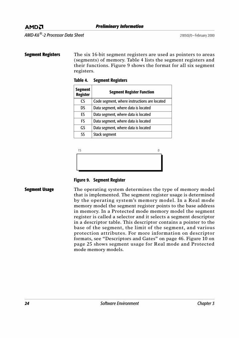
24 Software Environment Chapter 3
AMD-K6®-2 Processor Data Sheet 21850J/0—February 2000
Preliminary Information
Segment Registers The six 16-bit segment registers are used as pointers to areas
(segments) of memory. Table 4 lists the segment registers and
their functions. Figure 9 shows the format for all six segment
registers.
Figure 9. Segment Register
Segment Usage The operating system determines the type of memory model
that is implemented. The segment register usage is determined
by the operating system’s memory model. In a Real mode
memory model the segment register points to the base address
in memory. In a Protected mode memory model the segment
register is called a selector and it selects a segment descriptor
in a descriptor table. This descriptor contains a pointer to the
base of the segment, the limit of the segment, and various
protection attributes. For more information on descriptor
formats, see “Descriptors and Gates” on page 46. Figure 10 on
page 25 shows segment usage for Real mode and Protected
mode memory models.
Table 4. Segment Registers
SegmentRegister
Segment Register Function
CS Code segment, where instructions are located
DS Data segment, where data is located
ES Data segment, where data is located
FS Data segment, where data is located
GS Data segment, where data is located
SS Stack segment
015

Chapter 3 Software Environment 25
21850J/0—February 2000 AMD-K6®-2 Processor Data Sheet
Preliminary Information
Figure 10. Segment Usage
Instruction Pointer The instruction pointer (EIP or IP) is used in conjunction with
the code segment register (CS). The instruction pointer is
either a 32-bit register (EIP) or a 16-bit register (IP) that keeps
track of where the next instruction resides within memory. This
register cannot be directly manipulated, but can be altered by
modifying return pointers when a JMP or CALL instruction is
used.
Floating-Point Registers
The floating-point execution unit in the AMD-K6-2 processor is
designed to perform mathematical operations on non-integer
numbers. This floating-point unit conforms to the IEEE 754 and
854 standards and uses several registers to meet these
standards—eight numeric floating-point registers, a status
word register, a control word register, and a tag word register.
Segment Register
Real Mode Memory Model
Segment Selector
Physical Memory
Protected Mode Memory Model
Base
Descriptor Table
Physical Memory
Segment Base
Base
Limit
BaseLimit
Segment Base

26 Software Environment Chapter 3
AMD-K6®-2 Processor Data Sheet 21850J/0—February 2000
Preliminary Information
The eight floating-point registers are physically 80 bits wide
and labeled FPR0–FPR7. Figure 11 shows the format of these
floating-point registers. See “Floating-Point Register Data
Types” on page 28 for information on allowable floating-point
data types.
Figure 11. Floating-Point Register
The 16-bit FPU status word register contains information about
the state of the floating-point unit. Figure 12 shows the format
of this register.
Figure 12. FPU Status Word Register
64 63 07879
Sign Exponent Significand
9 8 7 6 5 4 3 2 1 0101112131415
PE
OE
ES
C0
C1
IE
ZE
UE
SFTOSP
C3
B C2
DE
Symbol Description BitsB FPU Busy 15
C3 Condition Code 14
TOSP Top of Stack Pointer 13–11C2 Condition Code 10
C1 Condition Code 9
C0 Condition Code 8ES Error Summary Status 7
SF Stack Fault 6
Exception FlagsPE Precision Error 5
UE Underflow Error 4
OE Overflow Error 3
ZE Zero Divide Error 2DE Denormalized Operation Error 1
IE Invalid Operation Error 0
TOSP Information000 = FPR0
111 = FPR7

Chapter 3 Software Environment 27
21850J/0—February 2000 AMD-K6®-2 Processor Data Sheet
Preliminary Information
The FPU control word register allows a programmer to manage
the FPU processing options. Figure 13 shows the format of this
register.
Figure 13. FPU Control Word Register
The FPU tag word register contains information about the
registers in the register stack. Figure 14 shows the format of this
register.
Figure 14. FPU Tag Word Register
9 8 7 6 5 4 3 2 1 0101112131415
PM
OM
PC
RC
IM
ZM
UM
DM
Rounding Control Information00b = Round to the nearest or even number
01b = Round down toward negative infinity
10b = Round up toward positive infinity11b = Truncate toward zero
Y
Precision Control Information
00b = 24 bits Single Precision Real
01b = Reserved10b = 53 bits Double Precision Real
11b = 64 bits Extended Precision Real
Reserved
Symbol Description Bits
Y Infinity Bit (80287 compatibility) 12
RC Rounding Control 11–10PC Precision Control 9–8
Exception Masks
PM Precision 5UM Underflow 4
OM Overflow 3
ZM Zero Divide 2DM Denormalized Operation 1
IM Invalid Operation 0
Tag Values00 = Valid
01 = Zero
10 = Special11 = Empty
8 7 6 5 4 3 2 1 0101112131415
TAG(FPR7)
TAG(FPR6)
TAG(FPR4)
TAG(FPR5)
TAG(FPR2)
TAG(FPR3)
TAG(FPR0)
TAG(FPR1)
9

28 Software Environment Chapter 3
AMD-K6®-2 Processor Data Sheet 21850J/0—February 2000
Preliminary Information
Floating-Point Register Data Types
Floating-point registers use four different types of data—
packed decimal, single-precision real, double-precision real,
and extended-precision real. Figures 15 and 16 show the
formats for these registers.
Figure 15. Packed Decimal Data Register
Figure 16. Precision Real Data Registers
079
Precision — 18 Digits, 72 Bits Used, 4-Bits/Digit
71
SIgnore
or Zero
78 72
Description Bits
Ignored on Load, Zeros on Store 78-72
Sign Bit 79
063Double-Precision Real
31 0Single-Precision Real
079
22
S Biased
Exponent
78
23
SBiased
Exponent
6364
5152
Biased
ExponentS
Significand
Significand
Significand
30
62
Extended-Precision Real
S = Sign Bit
S = Sign Bit
S = Sign Bit
I
62
I = Integer Bit

Chapter 3 Software Environment 29
21850J/0—February 2000 AMD-K6®-2 Processor Data Sheet
Preliminary Information
MMX™/3DNow!™ Registers
The AMD-K6-2 processor implements e ight 64 -bi t
MMX/3DNow! registers for use by multimedia software. These
registers are mapped on the floating-point register stack. The
MMX and 3DNow! instructions refer to these registers as mm0
to mm7. Figure 17 shows the format of these registers. For more
information, see the AMD-K6® Processor Multimedia Technology
Manual, order# 20726 and the 3DNow!™ Technology Manual,
order# 21928.
Figure 17. MMX™/3DNow!™ Registers
MMX™ Data Types For the MMX instructions, the MMX registers use three types of
data—packed eight-byte integer, packed quadword integer, and
packed dual doubleword integer. Figure 18 on page 30 shows
the format of these data types.
63 0
mm0
mm7
mm1
mm6
mm5
mm2
mm3
mm4

30 Software Environment Chapter 3
AMD-K6®-2 Processor Data Sheet 21850J/0—February 2000
Preliminary Information
Figure 18. MMX™ Data Types
3DNow!™ Data Types For 3DNow! instructions, the MMX/3DNow! registers use
packed single-precision real data. Figure 19 shows the format of
the 3DNow! data type.
Figure 19. 3DNow!™ Data Types
63 0
Packed Bytes Integer
63 0Packed Words Integer
63 0
Packed Doubleword Integer
32 31
48 47 32 31 16 15
56 55 48 47 40 39 32 31 24 23 16 15 8 7
Byte 7 Byte 6 Byte 5 Byte 4 Byte 3 Byte 2 Byte 1 Byte 0
Word 0Word 1Word 2Word 3
Doubleword 1 Doubleword 0
63 62 032 31 30
Packed Single Precision Floating Point
55 54 23 22
Biased
ExponentS Significand
S = Sign Bit
Biased
ExponentS Significand
S = Sign Bit

Chapter 3 Software Environment 31
21850J/0—February 2000 AMD-K6®-2 Processor Data Sheet
Preliminary Information
EFLAGS Register The EFLAGS register provides for three different types of
flags—system, control, and status. The system flags provide
operating system controls, the control flag provides directional
information for string operations, and the status flags provide
information resulting from logical and arithmetic operations.
Figure 20 shows the format of this register.
Figure 20. EFLAGS Registers
9 8 7 6 5 4 3 2 1 0101112131415161718192021
IOPL
31 30 29 28 27 26 25 24 23 22
AF
PF
ZF
SF
IF
DF
TF
OF
NT
RF
VM
AC
VIF
VIP
ID
CF
Reserved
Symbol Description BitsID ID Flag 21
VIP Virtual Interrupt Pending 20
VIF Virtual Interrupt Flag 19AC Alignment Check 18
VM Virtual-8086 Mode 17
RF Resume Flag 16NT Nested Task 14
IOPL I/O Privilege Level 13–12
OF Overflow Flag 11DF Direction Flag 10
IF Interrupt Flag 9
TF Trap Flag 8SF Sign Flag 7
ZF Zero Flag 6
AF Auxiliary Flag 4PF Parity Flag 2
CF Carry Flag 0

32 Software Environment Chapter 3
AMD-K6®-2 Processor Data Sheet 21850J/0—February 2000
Preliminary Information
Control Registers The five control registers contain system control bits and
pointers. Figures 21 through 25 show the formats of these
registers.
Figure 21. Control Register 4 (CR4)
Figure 22. Control Register 3 (CR3)
Figure 23. Control Register 2 (CR2)
7 6 5 4 3 2 1 031
PSE
TSD
MCE
VME
DE
PVI
Reserved
Symbol Description Bit
MCE Machine Check Enable 6
PSE Page Size Extensions 4DE Debugging Extensions 3
TSD Time Stamp Disable 2
PVI Protected Virtual Interrupts 1VME Virtual-8086 Mode Extensions 0
PCD
9 8 7 6 5 4 3 2 1 010111213141516171819202131 30 29 28 27 26 25 24 23 22
Page Directory BasePWT
Reserved
Symbol Description Bit
PCD Page Cache Disable 4
PWT Page Writethrough 3
031
Page Fault Linear Address
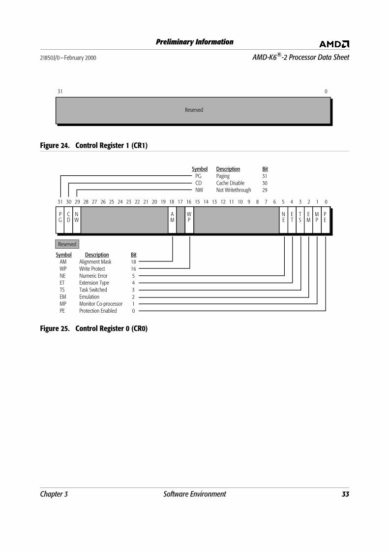
Chapter 3 Software Environment 33
21850J/0—February 2000 AMD-K6®-2 Processor Data Sheet
Preliminary Information
Figure 24. Control Register 1 (CR1)
Figure 25. Control Register 0 (CR0)
031
Reserved
ET
TS
9 8 7 6 5 4 3 2 1 010111213141516171819202131 30 29 28 27 26 25 24 23 22
AM
EM
WP
MP
PE
NE
PG
CD
NW
Reserved
Symbol Description BitAM Alignment Mask 18
WP Write Protect 16
NE Numeric Error 5ET Extension Type 4
TS Task Switched 3
EM Emulation 2MP Monitor Co-processor 1
PE Protection Enabled 0
Symbol Description Bit
PG Paging 31
CD Cache Disable 30NW Not Writethrough 29

34 Software Environment Chapter 3
AMD-K6®-2 Processor Data Sheet 21850J/0—February 2000
Preliminary Information
Debug Registers Figures 26 through 29 show the 32-bit debug registers
supported by the processor.
Figure 26. Debug Register DR7
9 8 7 6 5 4 3 2 1 0101112131415
L2
L1
L3
G3
GE
LE
L0
G0
G1
L2
GD
25 24 23 22 21 20 19 18 17 16262728293031
R/W 3
LEN 3
R/W 2
LEN 2
R/W 1
LEN 1
R/W 0
LEN 0
Reserved
Symbol Description Bit
GD General Detect Enabled 13GE Global Exact Breakpoint Enabled 9
LE Local Exact Breakpoint Enabled 8
G3 Global Exact Breakpoint # 3 Enabled 7L3 Local Exact Breakpoint # 3 Enabled 6
G2 Global Exact Breakpoint # 2 Enabled 5
L2 Local Exact Breakpoint # 2 Enabled 4G1 Global Exact Breakpoint # 1 Enabled 3
L1 Local Exact Breakpoint # 1 Enabled 2
G0 Global Exact Breakpoint # 0 Enabled 1L0 Local Exact Breakpoint # 0 Enabled 0
Symbol Description Bits
LEN 3 Length of Breakpoint #3 31–30R/W 3 Type of Transaction(s) to Trap 29–28
LEN 2 Length of Breakpoint #2 27–26
R/W 2 Type of Transaction(s) to Trap 25–24LEN 1 Length of Breakpoint #1 23–22
R/W 1 Type of Transaction(s) to Trap 21–20
LEN 0 Length of Breakpoint #0 19–18R/W 0 Type of Transaction(s) to Trap 17–16

Chapter 3 Software Environment 35
21850J/0—February 2000 AMD-K6®-2 Processor Data Sheet
Preliminary Information
Figure 27. Debug Register DR6
Figure 28. Debug Registers DR5 and DR4
9 8 7 6 5 4 3 2 1 010111213141516171819202131 30 29 28 27 26 25 24 23 22
B1
B2
BS
B0
BT
BD
B3
Reserved
Symbol Description Bit
BT Breakpoint Task Switch 15
BS Breakpoint Single Step 14 BD Breakpoint Debug Access Detected 13
B3 Breakpoint #3 Condition Detected 3
B2 Breakpoint #2 Condition Detected 2 B1 Breakpoint #1 Condition Detected 1
B0 Breakpoint #0 Condition Detected 0
9 8 7 6 5 4 3 2 1 010111213141516171819202131 30 29 28 27 26 25 24 23 22
Reserved
DR5
9 8 7 6 5 4 3 2 1 010111213141516171819202131 30 29 28 27 26 25 24 23 22
Reserved
DR4

36 Software Environment Chapter 3
AMD-K6®-2 Processor Data Sheet 21850J/0—February 2000
Preliminary Information
Figure 29. Debug Registers DR3, DR2, DR1, and DR0
9 8 7 6 5 4 3 2 1 010111213141516171819202131 30 29 28 27 26 25 24 23 22
Breakpoint 3 32-bit Linear Address
DR3
9 8 7 6 5 4 3 2 1 010111213141516171819202131 30 29 28 27 26 25 24 23 22
Breakpoint 0 32-bit Linear Address
DR0
9 8 7 6 5 4 3 2 1 010111213141516171819202131 30 29 28 27 26 25 24 23 22
Breakpoint 2 32-bit Linear Address
DR2
9 8 7 6 5 4 3 2 1 010111213141516171819202131 30 29 28 27 26 25 24 23 22
Breakpoint 1 32-bit Linear Address
DR1

Chapter 3 Software Environment 37
21850J/0—February 2000 AMD-K6®-2 Processor Data Sheet
Preliminary Information
Model-Specific Registers (MSR)
The AMD-K6-2 processor Model 8/[7:0] provides seven MSRs.
The value in the ECX register selects the MSR to be addressed
by the RDMSR and WRMSR instructions. The values in EAX
and EDX are used as inputs and outputs by the RDMSR and
WRMSR instructions. Table 5 lists the MSRs and the
corresponding value of the ECX register. Figures 30 through 36
show the MSR formats.
For more information about the RDMSR and WRMSR
instructions, see the AMD K86™ Family BIOS and Software Tools
Development Guide, order# 21062.
MCAR and MCTR. The AMD-K6-2 processor does not support the
generation of a machine check exception. However, the
processor does provide a 64-bit machine check address register
(MCAR), a 64-bit machine check type register (MCTR), and a
machine check enable (MCE) bit in CR4. Because the processor
does not support machine check exceptions, the contents of the
MCAR and MCTR are only affected by the WRMSR instruction
and by RESET being sampled asserted (where all bits in each
register are reset to 0).
Figure 30. Machine-Check Address Register (MCAR)
Table 5. AMD-K6®-2 Processor Model 8/[7:0] MSRs
Model-Specific Register Value of ECX
Machine Check Address Register (MCAR) 00h
Machine Check Type Register (MCTR) 01h
Test Register 12 (TR12) 0Eh
Time Stamp Counter (TSC) 10h
Extended Feature Enable Register (EFER) C000_0080h
SYSCALL/SYSRET Target Address Register (STAR) C000_0081h
Write Handling Control Register (WHCR) C000_0082h
063
MCAR

38 Software Environment Chapter 3
AMD-K6®-2 Processor Data Sheet 21850J/0—February 2000
Preliminary Information
Figure 31. Machine-Check Type Register (MCTR)
Test Register 12 (TR12). Test register 12 provides a method for
disabling the L1 caches. Figure 32 shows the format of TR12.
Figure 32. Test Register 12 (TR12)
Time Stamp Counter. With each processor c lock cycle , the
processor increments the 64-bit time stamp counter (TSC) MSR.
Figure 33 shows the format of the TSC.
Figure 33. Time Stamp Counter (TSC)
5 4 063
MCTR
Reserved
4 2 1 063
CI
3
ReservedSymbol Description Bit
CI Cache Inhibit Bit 3
063
TSC

Chapter 3 Software Environment 39
21850J/0—February 2000 AMD-K6®-2 Processor Data Sheet
Preliminary Information
Extended Feature Enable Register (EFER)–Model 8[7:0]. The extended
feature enable register (EFER) contains the control bits that
enable the extended features of the AMD-K6-2 processor.
Figure 34 shows the format of the EFER register, and Table 6
defines the function of each bit in the EFER register.
Note: The EFER register as defined in the Model 8/[7:0] has
changed in the Model 8/[F:8]. See “Extended Feature Enable
Register (EFER)–Model 8/[F:8]” on page 50.
Figure 34. Extended Feature Enable Register (EFER)–Model 8[7:0]
SYSCALL/SYSRET Target Address Register (STAR). The SYSCALL/SYSRET target address register (STAR)
contains the target EIP address used by the SYSCALL
instruction and the 16-bit code and stack segment selector
bases used by the SYSCALL and SYSRET instructions. Figure
35 shows the format of the STAR register, and Table 7 on
page 40 defines the function of each bit of the STAR register.
For more information, see the SYSCALL and SYSRET Instruction
Specification Application Note, order# 21086.
Figure 35. SYSCALL/SYSRET Target Address Register (STAR)
1 063
SCE
Reserved
Symbol Description Bit
SCE System Call/Return Extension 0
Table 6. Extended Feature Enable Register (EFER)–Model 8[7:0]Definition
Bit Description R/W
63–1 Reserved R
0 System Call Extension (SCE) R/W
31 063
Target EIP Address
324748
SYSCALL CS Selector and SS
Selector Base
SYSRET CS Selector and SS
Selector Base

40 Software Environment Chapter 3
AMD-K6®-2 Processor Data Sheet 21850J/0—February 2000
Preliminary Information
Write Handling Control Register (WHCR)–Model 8/[7:0]. The write handling control register (WHCR) is a MSR that
contains three fields—the WCDE bit, write allocate enable
limit (WAELIM) field, and the write allocate enable
15-to-16-Mbyte (WAE15M) bit. Figure 36 shows the format of
WHCR. See “Write Allocate” on page 186 for more information.
Note: The WHCR register as defined in the Model 8/[7:0] has
changed in the Model 8/[F:8]. See “Write Handling Control
Register (WHCR)–Model 8/[F:8]” on page 51.
Figure 36. Write Handling Control Register (WHCR)–Model 8/[7:0]
Memory Management Registers
The AMD-K6-2 processor controls segmented memory
management with the registers listed in Table 8. Figure 37 on
page 41 shows the formats of these registers.
Table 7. SYSCALL/SYSRET Target Address Register (STAR) Definition
Bit Description R/W
63–48 SYSRET CS and SS Selector Base R/W
47–32 SYSCALL CS and SS Selector Base R/W
31–0 Target EIP Address R/W
7 1 063
WAELIM
8
0
Note: Hardware RESET initializes this MSR to all zeros.
WAE15M
Symbol Description Bits WCDE Always program to 0 8
WAELIM Write Allocate Enable Limit 7–1
WAE15M Write Allocate Enable 15-to-16-Mbyte 0
9
Reserved
Table 8. Memory Management Registers
Register Name Function
Global Descriptor Table Register Contains a pointer to the base of the global descriptor table
Interrupt Descriptor Table Register Contains a pointer to the base of the interrupt descriptor table
Local Descriptor Table Register Contains a pointer to the local descriptor table of the current task
Task Register Contains a pointer to the task state segment of the current task

Chapter 3 Software Environment 41
21850J/0—February 2000 AMD-K6®-2 Processor Data Sheet
Preliminary Information
Figure 37. Memory Management Registers
15 0
16-Bit Limit
1647
32-Bit Linear Base Address
Global and Interrupt Descriptor Table Registers
31 063
32-Bit Limit
32
32-Bit Linear Base Address
15 0
Local Descriptor Table Register and Task Register
Attributes
15 0
Selector

42 Software Environment Chapter 3
AMD-K6®-2 Processor Data Sheet 21850J/0—February 2000
Preliminary Information
Task State Segment Figure 38 shows the format of the task state segment (TSS).
Figure 38. Task State Segment (TSS)
31
Interrupt Redirection Bitmap (IRB)
(eight 32-bit locations)
0
I/O Permission Bitmap (IOPB)
(up to 8 Kbytes)
Operating SystemData Structure
Base Address of IOPB
LDT Selector0000h
0000h
0000h
0000h
0000h
0000h
0000h
GS
FS
DS
SS
CS
ES
EDI
ESI
EBP
ESP
EBX
EDX
ECX
EAX
CR3
EFLAGS
EIP
0000h
0000h
0000h
0000h
SS2
SS1
SS0
Link (Prior TSS Selector)
ESP0
ESP1
ESP2
TSS Limit from TR
64h
0
T0000h

Chapter 3 Software Environment 43
21850J/0—February 2000 AMD-K6®-2 Processor Data Sheet
Preliminary Information
Paging The AMD-K6-2 processor can physically address up to four
Gbytes of memory. This memory can be segmented into pages.
The size of these pages is determined by the operating system
design and the values set up in the page directory entries (PDE)
and page table entries (PTE). The processor can access both
4-Kbyte pages and 4-Mbyte pages, and the page sizes can be
intermixed within a page directory. When the page size
extension (PSE) bit in CR4 is set, the processor translates linear
addresses using either the 4-Kbyte translation lookaside buffer
(TLB) or the 4-Mbyte TLB, depending on the state of the page
size (PS) bit in the page directory entry. Figures 39 and 40 show
how 4-Kbyte and 4-Mbyte page translations work.
Figure 39. 4-Kbyte Paging Mechanism
Linear Address
PageDirectory
PageTable
4-Kbyte
PageFrame
CR3
011122131 22
Page Directory
Offset
Page Table
OffsetPage Offset
PDE
PTE
Physical Address

44 Software Environment Chapter 3
AMD-K6®-2 Processor Data Sheet 21850J/0—February 2000
Preliminary Information
Figure 40. 4-Mbyte Paging Mechanism
Figures 41 through 43 show the formats of the PDE and PTE.
These entries contain information regarding the location of
pages and their status.
Linear Address
Page
Directory
4-Mbyte
PageFrame
CR3
02131 22
Page Directory
OffsetPage
Offset
PDE
PhysicalAddress

Chapter 3 Software Environment 45
21850J/0—February 2000 AMD-K6®-2 Processor Data Sheet
Preliminary Information
Figure 41. Page Directory Entry 4-Kbyte Page Table (PDE)
Figure 42. Page Directory Entry 4-Mbyte Page Table (PDE)
8 7 6 5 4 3 2 1 031
PCD
U/S
W/R
9101112
AVL
0 APWT
PPage Table Base Address
Symbol Description Bits
AVL Available to Software 11–9
Reserved 8 PS Page Size 7
Reserved 6
A Accessed 5PCD Page Cache Disable 4
PWT Page Writethrough 3
U/S User/Supervisor 2W/R Write/Read 1
P Present (valid) 0
8 7 6 5 4 3 2 1 031
PCD
U/S
W/R
9101112
AVL
1 APWT
PPhysical Page Base Address Reserved
2122
Symbol Description Bits
AVL Available to Software 11–9 Reserved 8
PS Page Size 7
Reserved 6 A Accessed 5
PCD Page Cache Disable 4
PWT Page Writethrough 3U/S User/Supervisor 2
W/R Write/Read 1
P Present (valid) 0

46 Software Environment Chapter 3
AMD-K6®-2 Processor Data Sheet 21850J/0—February 2000
Preliminary Information
Figure 43. Page Table Entry (PTE)
Descriptors and Gates There are various types of structures and registers in the x86
architecture that define, protect, and isolate code segments,
data segments, task state segments, and gates. These structures
are called descriptors.
Figure 44 on page 47 shows the application segment descriptor
format. Table 9 contains information describing the memory
segment type to which the descriptor points. The application
segment descriptor is used to point to either a data or code
segment.
Figure 45 on page 48 shows the system segment descriptor
format. Table 10 contains information describing the type of
segment or gate to which the descriptor points. The system
segment descriptor is used to point to a task state segment, a
call gate, or a local descriptor table.
The AMD-K6-2 processor uses gates to transfer control between
executable segments with different privilege levels. Figure 46
on page 49 shows the format of the gate descriptor types. Table
10 contains information describing the type of segment or gate
to which the descriptor points.
8 7 6 5 4 3 2 1 031
PCD
U/S
W/R
9101112
AVL
APWT
PPhysical Page Base Address D
Symbol Description Bits
AVL Available to Software 11–9 Reserved 8–7
D Dirty 6
A Accessed 5PCD Page Cache Disable 4
PWT Page Writethrough 3
U/S User/Supervisor 2W/R Write/Read 1
P Present (valid) 0
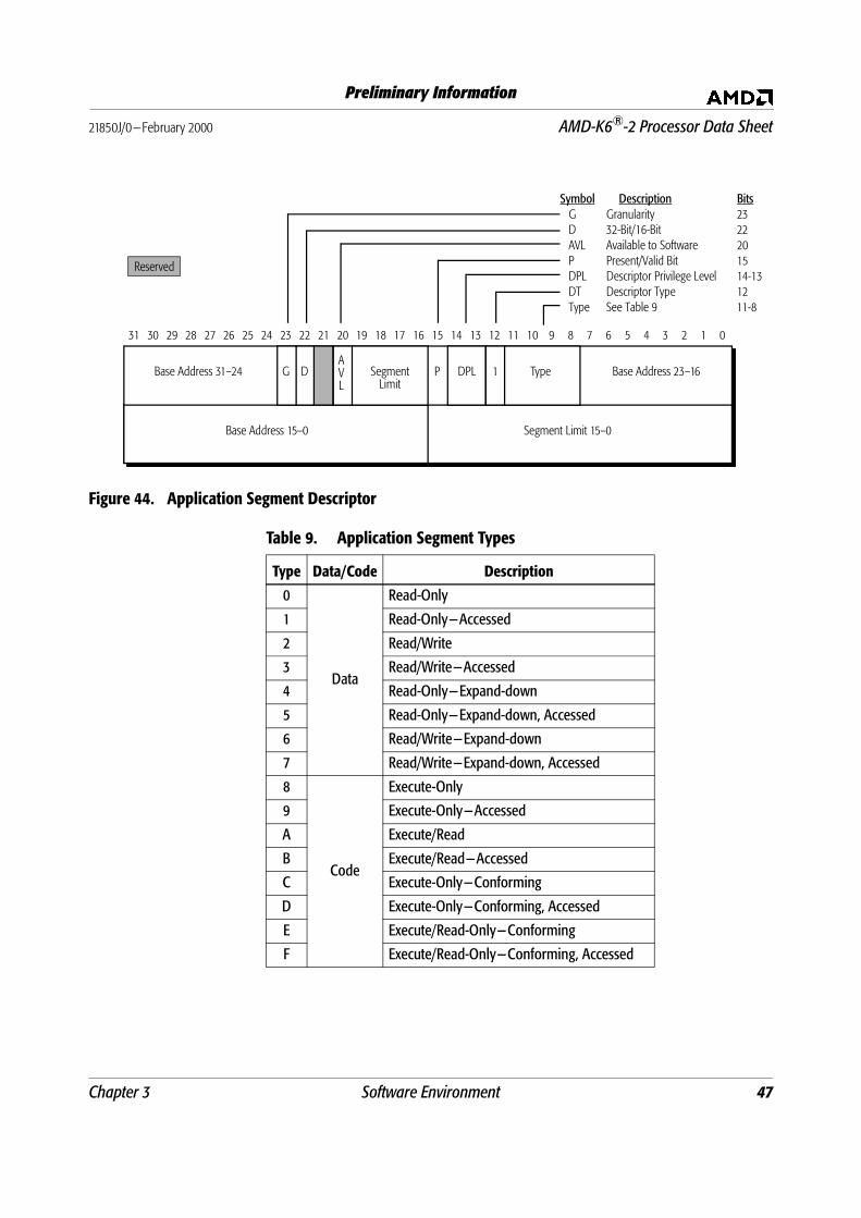
Chapter 3 Software Environment 47
21850J/0—February 2000 AMD-K6®-2 Processor Data Sheet
Preliminary Information
Figure 44. Application Segment Descriptor
Base Address 15–0 Segment Limit 15–0
9 8 7 6 5 4 3 2 1 010111213141516171819202131 30 29 28 27 26 25 24 23 22
Segment Limit
P DPL 1 TypeAVL
G DBase Address 31–24 Base Address 23–16
Reserved
Symbol Description Bits
G Granularity 23D 32-Bit/16-Bit 22
AVL Available to Software 20
P Present/Valid Bit 15DPL Descriptor Privilege Level 14-13
DT Descriptor Type 12
Type See Table 9 11-8
Table 9. Application Segment Types
Type Data/Code Description
0
Data
Read-Only
1 Read-Only—Accessed
2 Read/Write
3 Read/Write—Accessed
4 Read-Only—Expand-down
5 Read-Only—Expand-down, Accessed
6 Read/Write—Expand-down
7 Read/Write—Expand-down, Accessed
8
Code
Execute-Only
9 Execute-Only—Accessed
A Execute/Read
B Execute/Read—Accessed
C Execute-Only—Conforming
D Execute-Only—Conforming, Accessed
E Execute/Read-Only—Conforming
F Execute/Read-Only—Conforming, Accessed

48 Software Environment Chapter 3
AMD-K6®-2 Processor Data Sheet 21850J/0—February 2000
Preliminary Information
Figure 45. System Segment Descriptor
Base Address 15–0 Segment Limit 15–0
9 8 7 6 5 4 3 2 1 010111213141516171819202131 30 29 28 27 26 25 24 23 22
Segment Limit
P DPL 0 TypeAVL
G XBase Address 31–24 Base Address 23–16
Reserved
Symbol Description BitsG Granularity 23
X Not Needed 22
AVL Availability to Software 20P Present/Valid Bit 15
DPL Descriptor Privilege Level 14-13
DT Descriptor Type 12Type See Table 10 11-8
Table 10. System Segment and Gate Types
Type Description
0 Reserved
1 Available 16-bit TSS
2 LDT
3 Busy 16-bit TSS
4 16-bit Call Gate
5 Task Gate
6 16-bit Interrupt Gate
7 16-bit Trap Gate
8 Reserved
9 Available 32-bit TSS
A Reserved
B Busy 32-bit TSS
C 32-bit Call Gate
D Reserved
E 32-bit Interrupt Gate
F 32-bit Trap Gate

Chapter 3 Software Environment 49
21850J/0—February 2000 AMD-K6®-2 Processor Data Sheet
Preliminary Information
Figure 46. Gate Descriptor
Exceptions and Interrupts
Table 11 summarizes the exceptions and interrupts.
DPL 0 TypeOffset 31–16 P
Segment Selector Offset 15–0
9 8 7 6 5 4 3 2 1 010111213141516171819202131 30 29 28 27 26 25 24 23 22
Reserved
Symbol Description Bits
P Present/Valid Bit 15
DPL Descriptor Privilege Level 14-13DT Descriptor Type 12
Type See Table 10 11-8
Table 11. Summary of Exceptions and Interrupts
InterruptNumber
Interrupt Type Cause
0 Divide by Zero Error DIV, IDIV
1 Debug Debug trap or fault
2 Non-Maskable Interrupt NMI signal sampled asserted
3 Breakpoint Int 3
4 Overflow INTO
5 Bounds Check BOUND
6 Invalid Opcode Invalid instruction
7 Device Not Available ESC and WAIT
8 Double Fault Fault occurs while handling a fault
9 Reserved - Interrupt 13 —
10 Invalid TSS Task switch to an invalid segment
11 Segment Not Present Instruction loads a segment and present bit is 0 (invalid segment)
12 Stack Segment Stack operation causes limit violation or present bit is 0
13 General Protection Segment related or miscellaneous invalid actions
14 Page Fault Page protection violation or a reference to missing page
16 Floating-Point Error Arithmetic error generated by floating-point instruction
17 Alignment CheckData reference to an unaligned operand. (The AC flag and the AM bit of CR0 are set to 1.)
0–255 Software Interrupt INT n

50 Software Environment Chapter 3
AMD-K6®-2 Processor Data Sheet 21850J/0—February 2000
Preliminary Information
3.2 AMD-K6®-2 Processor Model 8/[F:8] Registers
AMD-K6-2 processor Model 8/[F:8] implements the same seven
MSRs as the Model 8/[7:0], but the bits and fields within the
EFER and WHCR MSRs are not defined identically. Model
8/[F:8] also supports three additional MSRs: UWCCR, PSOR,
and PFIR. For more information, see the AMD-K6® Processor
BIOS Design Application Note, order# 21329. Table 12 lists the
MSRs and the corresponding value of the ECX register.
Extended Feature Enable Register (EFER)–Model 8/[F:8]
The Extended Feature Enable Register (EFER) contains the
control bits that enable the extended features of the processor.
Figure 47 shows the format of the EFER register, and Table 13
on page 51 defines the function of each bit of the EFER
register.
Note: The EFER register as defined in the Model 8/[7:0] has
changed in the Model 8/[F:8]. See “Extended Feature Enable
Register (EFER)–Model 8[7:0]” on page 39.
Table 12. AMD-K6®-2 Processor Model 8/[F:8] MSRs
Model-Specific Register Value of ECX
Machine Check Address Register (MCAR) 00h
Machine Check Type Register (MCTR) 01h
Test Register 12 (TR12) 0Eh
Time Stamp Counter (TSC) 10h
Extended Feature Enable Register (EFER) C000_0080h
SYSCALL/SYSRET Target Address Register (STAR) C000_0081h
Write Handling Control Register (WHCR) C000_0082h
UC/WC Cacheability Control Register (UWCCR) C000_0085h
Processor State Observability Register (PSOR) C000_0087h
Page Flush/Invalidate Register (PFIR) C000_0088h

Chapter 3 Software Environment 51
21850J/0—February 2000 AMD-K6®-2 Processor Data Sheet
Preliminary Information
Figure 47. Extended Feature Enable Register (EFER)—Model 8/[F:8]
For more information on EWBEC, see “EWBE Control” on page
201.
Write Handling Control Register (WHCR)–Model 8/[F:8]
The Write Handling Control Register (WHCR) is a MSR that
contains two fields —the Write Allocate Enable Limit
(WAELIM) field, and the Write Allocate Enable 15-to-16-Mbyte
(WAE15M) bit (see Figure 48). For more information, see
“Write Allocate” on page 186.
Note: The WHCR register as defined in the Model 8/[7:0] has
changed in the Model 8/[F:8]. See “Write Handling Control
Register (WHCR)–Model 8/[7:0]” on page 40.
Table 13. Extended Feature Enable Register (EFER)–Model 8/[F:8] Definition
Bit Description R/W Function
63–4 Reserved RWriting a 1 to any reserved bit causes a general protectionfault to occur. All reserved bits are always read as 0.
3-2 EWBE Control (EWBEC) R/W
This 2-bit field controls the behavior of the processor withrespect to the ordering of write cycles and the EWBE# signal.EFER[3] and EFER[2] are Global EWBE Disable (GEWBED)and Speculative EWBE Disable (SEWBED), respectively.
1 Data Prefetch Enable (DPE) R/W
DPE must be set to 1 to enable data prefetching (this is thedefault setting following reset). If enabled, cache missesinitiated by a memory read within a 32-byte cache line areconditionally followed by cache-line fetches of the other linein the 64-byte sector.
0 System Call Extension (SCE) R/WSCE must be set to 1 to enable the usage of the SYSCALL andSYSRET instructions.
1 063
SCE
Reserved
234
DPE
EWBEC
Symbol Description Bit
EWBEC EWBE Control 3-2DPE Data Prefetch Enable 1
SCE System Call Extension 0

52 Software Environment Chapter 3
AMD-K6®-2 Processor Data Sheet 21850J/0—February 2000
Preliminary Information
Figure 48. Write Handling Control Register (WHCR)—Model 8/[F:8]
UC/WC Cacheability Control Register(UWCCR)
The AMD-K6-2 processor Model 8/[F:8] provides two variable-
range Memory Type Range Registers (MTRRs)—MTRR0 and
MTRR1—that each specify a range of memory. Each range can
be defined as uncacheable (UC) or write-combining (WC)
memory. For more detailed information on UWCCR, see
“UC/WC Cacheability Control Register (UWCCR)” on page
203.
.
Figure 49. UC/WC Cacheability Control Register (UWCCR)
1522 063
Reserved
WAELIM
16
Note: Hardware RESET initializes this MSR to all zeros.
WAE15M
Symbol Description Bits
WAELIM Write Allocate Enable Limit 31-22WAE15M Write Allocate Enable 15-to-16-Mbyte 16
17213132
16 063
Physical Address Mask 0
1731
Physical Base Address 0
12
Physical Address Mask 1Physical Base Address 1
3233344849
U
C
0
W
C
0
U
C
1
W
C
1
MTRR1 MTRR0
Symbol Description Bits
UC0 Uncacheable Memory Type 0WC0 Write-Combining Memory Type 1
Symbol Description Bits
UC1 Uncacheable Memory Type 32WC1 Write-Combining Memory Type 33

Chapter 3 Software Environment 53
21850J/0—February 2000 AMD-K6®-2 Processor Data Sheet
Preliminary Information
Processor State Observability Register (PSOR)
The AMD-K6-2 processor Model 8/[F:8] provides the Processor
State Observability Register (PSOR) (see Figure 50).
Figure 50. Processor State Observability Register (PSOR)
Page Flush/Invalidate Register (PFIR)
The AMD-K6-2 processor Model 8/[F:8] contains the Page
Flush/Invalidate Register (PFIR) (see Figure 51) that allows
cache invalidation and optional flushing of a specific 4-Kbyte
page from the linear address space. For more detailed
information on PFIR, see “PFIR” on page 195.
Figure 51. Page Flush/Invalidate Register (PFIR)
2 063
BF
Reserved
Symbol Description Bit
NOL2 No L2 Functionality 8STEP Processor Stepping 7-4
BF Bus Frequency Divisor 2-0
34
STEP
789
NOL2
LINPAGE
1 063
F/I
Reserved
Symbol Description Bit
LINPAGE 20-bit Linear Page Address 31-12PF Page Fault Occurred 8
F/I Flush/Invalidate Command 0
1131 1232
PF
9 8 7

54 Software Environment Chapter 3
AMD-K6®-2 Processor Data Sheet 21850J/0—February 2000
Preliminary Information
3.3 Instructions Supported by the AMD-K6®-2 Processor
This section documents all of the x86 instructions supported by
the AMD-K6-2 processor. The following tables show the
instruction mnemonic, opcode, modR/M byte, decode type, and
RISC86 operation(s) for each instruction. Tables 14 through 17
define the integer, floating-point, MMX, and 3DNow!
instructions for the AMD-K6-2 processor, respectively.
The first column in these tables indicates the instruction
mnemonic and operand types with the following notations:
reg8—byte integer register defined by instruction byte(s) or
bits 5, 4, and 3 of the modR/M byte
mreg8—byte integer register or byte integer value in
memory defined by the modR/M byte
reg16/32—word or doubleword integer register defined by
instruction byte(s) or bits 5, 4, and 3 of the modR/M byte
mreg16/32—word or doubleword integer register, or word or
doubleword integer value in memory defined by the
modR/M byte
mem8—byte integer value in memory
mem16/32—word or doubleword integer value in memory
mem32/48—doubleword or 48-bit integer value in memory
mem48—48-bit integer value in memory
mem64—64-bit value in memory
imm8—8-bit immediate value
imm16/32—16-bit or 32-bit immediate value
disp8—8-bit displacement value
disp16/32—16-bit or 32-bit displacement value
disp32/48—doubleword or 48-bit displacement value
eXX—register width depending on the operand size
mem32real—32-bit floating-point value in memory
mem64real—64-bit floating-point value in memory
mem80real—80-bit floating-point value in memory
mmreg—MMX/3DNow! register
mmreg1—MMX/3DNow! register defined by bits 5, 4, and 3
of the modR/M byte
mmreg2—MMX/3DNow! register defined by bits 2, 1, and 0
of the modR/M byte

Chapter 3 Software Environment 55
21850J/0—February 2000 AMD-K6®-2 Processor Data Sheet
Preliminary Information
The second and third columns list all applicable opcode bytes.
The fourth column lists the modR/M byte when used by the
instruction. The modR/M byte defines the instruction as a
register or memory form. If modR/M bits 7 and 6 are documented
as mm (memory form), mm can only be 10b, 01b or 00b.
The fifth column lists the type of instruction decode—short,
long, and vector. The AMD-K6-2 processor decode logic can
process two short, one long, or one vector decode per clock.
The sixth column lists the type of RISC86 operation(s) required
for the instruction. The operation types and corresponding
execution units are as follows:
load, fload, mload—load unit
store, fstore, mstore—store unit
alu—either of the integer execution units
alux—integer X execution unit only
branch—branch condition unit
float—floating-point execution unit
meu—Multimedia execution units for MMX and 3DNow!
instructions
limm—load immediate, instruction control unit
Table 14. Integer Instructions
Instruction MnemonicFirst Byte
Second Byte
ModR/M Byte
DecodeType
RISC86Operations
AAA 37h vector
AAD D5h 0Ah vector
AAM D4h 0Ah vector
AAS 3Fh vector
ADC mreg8, reg8 10h 11-xxx-xxx vector
ADC mem8, reg8 10h mm-xxx-xxx vector
ADC mreg16/32, reg16/32 11h 11-xxx-xxx vector
ADC mem16/32, reg16/32 11h mm-xxx-xxx vector
ADC reg8, mreg8 12h 11-xxx-xxx vector
ADC reg8, mem8 12h mm-xxx-xxx vector
ADC reg16/32, mreg16/32 13h 11-xxx-xxx vector
ADC reg16/32, mem16/32 13h mm-xxx-xxx vector
ADC AL, imm8 14h vector

56 Software Environment Chapter 3
AMD-K6®-2 Processor Data Sheet 21850J/0—February 2000
Preliminary Information
ADC EAX, imm16/32 15h vector
ADC mreg8, imm8 80h 11-010-xxx vector
ADC mem8, imm8 80h mm-010-xxx vector
ADC mreg16/32, imm16/32 81h 11-010-xxx vector
ADC mem16/32, imm16/32 81h mm-010-xxx vector
ADC mreg16/32, imm8 (signed ext.) 83h 11-010-xxx vector
ADC mem16/32, imm8 (signed ext.) 83h mm-010-xxx vector
ADD mreg8, reg8 00h 11-xxx-xxx short alux
ADD mem8, reg8 00h mm-xxx-xxx long load, alux, store
ADD mreg16/32, reg16/32 01h 11-xxx-xxx short alu
ADD mem16/32, reg16/32 01h mm-xxx-xxx long load, alu, store
ADD reg8, mreg8 02h 11-xxx-xxx short alux
ADD reg8, mem8 02h mm-xxx-xxx short load, alux
ADD reg16/32, mreg16/32 03h 11-xxx-xxx short alu
ADD reg16/32, mem16/32 03h mm-xxx-xxx short load, alu
ADD AL, imm8 04h short alux
ADD EAX, imm16/32 05h short alu
ADD mreg8, imm8 80h 11-000-xxx short alux
ADD mem8, imm8 80h mm-000-xxx long load, alux, store
ADD mreg16/32, imm16/32 81h 11-000-xxx short alu
ADD mem16/32, imm16/32 81h mm-000-xxx long load, alu, store
ADD mreg16/32, imm8 (signed ext.) 83h 11-000-xxx short alux
ADD mem16/32, imm8 (signed ext.) 83h mm-000-xxx long load, alux, store
AND mreg8, reg8 20h 11-xxx-xxx short alux
AND mem8, reg8 20h mm-xxx-xxx long load, alux, store
AND mreg16/32, reg16/32 21h 11-xxx-xxx short alu
AND mem16/32, reg16/32 21h mm-xxx-xxx long load, alu, store
AND reg8, mreg8 22h 11-xxx-xxx short alux
AND reg8, mem8 22h mm-xxx-xxx short load, alux
AND reg16/32, mreg16/32 23h 11-xxx-xxx short alu
AND reg16/32, mem16/32 23h mm-xxx-xxx short load, alu
AND AL, imm8 24h short alux
AND EAX, imm16/32 25h short alu
Table 14. Integer Instructions (continued)
Instruction MnemonicFirst Byte
Second Byte
ModR/M Byte
DecodeType
RISC86Operations
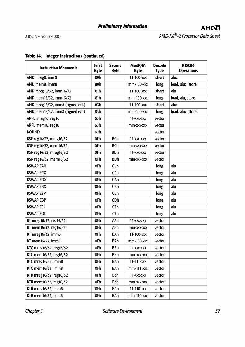
Chapter 3 Software Environment 57
21850J/0—February 2000 AMD-K6®-2 Processor Data Sheet
Preliminary Information
AND mreg8, imm8 80h 11-100-xxx short alux
AND mem8, imm8 80h mm-100-xxx long load, alux, store
AND mreg16/32, imm16/32 81h 11-100-xxx short alu
AND mem16/32, imm16/32 81h mm-100-xxx long load, alu, store
AND mreg16/32, imm8 (signed ext.) 83h 11-100-xxx short alux
AND mem16/32, imm8 (signed ext.) 83h mm-100-xxx long load, alux, store
ARPL mreg16, reg16 63h 11-xxx-xxx vector
ARPL mem16, reg16 63h mm-xxx-xxx vector
BOUND 62h vector
BSF reg16/32, mreg16/32 0Fh BCh 11-xxx-xxx vector
BSF reg16/32, mem16/32 0Fh BCh mm-xxx-xxx vector
BSR reg16/32, mreg16/32 0Fh BDh 11-xxx-xxx vector
BSR reg16/32, mem16/32 0Fh BDh mm-xxx-xxx vector
BSWAP EAX 0Fh C8h long alu
BSWAP ECX 0Fh C9h long alu
BSWAP EDX 0Fh CAh long alu
BSWAP EBX 0Fh CBh long alu
BSWAP ESP 0Fh CCh long alu
BSWAP EBP 0Fh CDh long alu
BSWAP ESI 0Fh CEh long alu
BSWAP EDI 0Fh CFh long alu
BT mreg16/32, reg16/32 0Fh A3h 11-xxx-xxx vector
BT mem16/32, reg16/32 0Fh A3h mm-xxx-xxx vector
BT mreg16/32, imm8 0Fh BAh 11-100-xxx vector
BT mem16/32, imm8 0Fh BAh mm-100-xxx vector
BTC mreg16/32, reg16/32 0Fh BBh 11-xxx-xxx vector
BTC mem16/32, reg16/32 0Fh BBh mm-xxx-xxx vector
BTC mreg16/32, imm8 0Fh BAh 11-111-xxx vector
BTC mem16/32, imm8 0Fh BAh mm-111-xxx vector
BTR mreg16/32, reg16/32 0Fh B3h 11-xxx-xxx vector
BTR mem16/32, reg16/32 0Fh B3h mm-xxx-xxx vector
BTR mreg16/32, imm8 0Fh BAh 11-110-xxx vector
BTR mem16/32, imm8 0Fh BAh mm-110-xxx vector
Table 14. Integer Instructions (continued)
Instruction MnemonicFirst Byte
Second Byte
ModR/M Byte
DecodeType
RISC86Operations

58 Software Environment Chapter 3
AMD-K6®-2 Processor Data Sheet 21850J/0—February 2000
Preliminary Information
BTS mreg16/32, reg16/32 0Fh ABh 11-xxx-xxx vector
BTS mem16/32, reg16/32 0Fh ABh mm-xxx-xxx vector
BTS mreg16/32, imm8 0Fh BAh 11-101-xxx vector
BTS mem16/32, imm8 0Fh BAh mm-101-xxx vector
CALL full pointer 9Ah vector
CALL near imm16/32 E8h short store
CALL mem16:16/32 FFh 11-011-xxx vector
CALL near mreg32 (indirect) FFh 11-010-xxx vector
CALL near mem32 (indirect) FFh mm-010-xxx vector
CBW/CWDE EAX 98h vector
CLC F8h vector
CLD FCh vector
CLI FAh vector
CLTS 0Fh 06h vector
CMC F5h vector
CMP mreg8, reg8 38h 11-xxx-xxx short alux
CMP mem8, reg8 38h mm-xxx-xxx short load, alux
CMP mreg16/32, reg16/32 39h 11-xxx-xxx short alu
CMP mem16/32, reg16/32 39h mm-xxx-xxx short load, alu
CMP reg8, mreg8 3Ah 11-xxx-xxx short alux
CMP reg8, mem8 3Ah mm-xxx-xxx short load, alux
CMP reg16/32, mreg16/32 3Bh 11-xxx-xxx short alu
CMP reg16/32, mem16/32 3Bh mm-xxx-xxx short load, alu
CMP AL, imm8 3Ch short alux
CMP EAX, imm16/32 3Dh short alu
CMP mreg8, imm8 80h 11-111-xxx short alux
CMP mem8, imm8 80h mm-111-xxx short load, alux
CMP mreg16/32, imm16/32 81h 11-111-xxx short alu
CMP mem16/32, imm16/32 81h mm-111-xxx short load, alu
CMP mreg16/32, imm8 (signed ext.) 83h 11-111-xxx long load, alu
CMP mem16/32, imm8 (signed ext.) 83h mm-111-xxx long load, alu
CMPSB mem8, mem8 A6h vector
CMPSW mem16, mem32 A7h vector
Table 14. Integer Instructions (continued)
Instruction MnemonicFirst Byte
Second Byte
ModR/M Byte
DecodeType
RISC86Operations

Chapter 3 Software Environment 59
21850J/0—February 2000 AMD-K6®-2 Processor Data Sheet
Preliminary Information
CMPSD mem32, mem32 A7h vector
CMPXCHG mreg8, reg8 0Fh B0h 11-xxx-xxx vector
CMPXCHG mem8, reg8 0Fh B0h mm-xxx-xxx vector
CMPXCHG mreg16/32, reg16/32 0Fh B1h 11-xxx-xxx vector
CMPXCHG mem16/32, reg16/32 0Fh B1h mm-xxx-xxx vector
CMPXCHG8B EDX:EAX 0Fh C7h 11-xxx-xxx vector
CMPXCHG8B mem64 0Fh C7h mm-xxx-xxx vector
CPUID 0Fh A2h vector
CWD/CDQ EDX, EAX 99h vector
DAA 27h vector
DAS 2Fh vector
DEC EAX 48h short alu
DEC ECX 49h short alu
DEC EDX 4Ah short alu
DEC EBX 4Bh short alu
DEC ESP 4Ch short alu
DEC EBP 4Dh short alu
DEC ESI 4Eh short alu
DEC EDI 4Fh short alu
DEC mreg8 FEh 11-001-xxx vector
DEC mem8 FEh mm-001-xxx long load, alux, store
DEC mreg16/32 FFh 11-001-xxx vector
DEC mem16/32 FFh mm-001-xxx long load, alu, store
DIV AL, mreg8 F6h 11-110-xxx vector
DIV AL, mem8 F6h mm-110-xxx vector
DIV EAX, mreg16/32 F7h 11-110-xxx vector
DIV EAX, mem16/32 F7h mm-110-xxx vector
IDIV mreg8 F6h 11-111-xxx vector
IDIV mem8 F6h mm-111-xxx vector
IDIV EAX, mreg16/32 F7h 11-111-xxx vector
IDIV EAX, mem16/32 F7h mm-111-xxx vector
IMUL reg16/32, imm16/32 69h 11-xxx-xxx vector
IMUL reg16/32, mreg16/32, imm16/32 69h 11-xxx-xxx vector
Table 14. Integer Instructions (continued)
Instruction MnemonicFirst Byte
Second Byte
ModR/M Byte
DecodeType
RISC86Operations

60 Software Environment Chapter 3
AMD-K6®-2 Processor Data Sheet 21850J/0—February 2000
Preliminary Information
IMUL reg16/32, mem16/32, imm16/32 69h mm-xxx-xxx vector
IMUL reg16/32, imm8 (sign extended) 6Bh 11-xxx-xxx vector
IMUL reg16/32, mreg16/32, imm8 (signed)
6Bh 11-xxx-xxx vector
IMUL reg16/32, mem16/32, imm8 (signed)
6Bh mm-xxx-xxx vector
IMUL AX, AL, mreg8 F6h 11-101-xxx vector
IMUL AX, AL, mem8 F6h mm-101-xxx vector
IMUL EDX:EAX, EAX, mreg16/32 F7h 11-101-xxx vector
IMUL EDX:EAX, EAX, mem16/32 F7h mm-101-xxx vector
IMUL reg16/32, mreg16/32 0Fh AFh 11-xxx-xxx vector
IMUL reg16/32, mem16/32 0Fh AFh mm-xxx-xxx vector
IN AL, imm8 E4h vector
IN AX, imm8 E5h vector
IN EAX, imm8 E5h vector
IN AL, DX ECh vector
IN AX, DX EDh vector
IN EAX, DX EDh vector
INC EAX 40h short alu
INC ECX 41h short alu
INC EDX 42h short alu
INC EBX 43h short alu
INC ESP 44h short alu
INC EBP 45h short alu
INC ESI 46h short alu
INC EDI 47h short alu
INC mreg8 FEh 11-000-xxx vector
INC mem8 FEh mm-000-xxx long load, alux, store
INC mreg16/32 FFh 11-000-xxx vector
INC mem16/32 FFh mm-000-xxx long load, alu, store
INVD 0Fh 08h vector
INVLPG 0Fh 01h mm-111-xxx vector
JO short disp8 70h short branch
JB/JNAE short disp8 71h short branch
Table 14. Integer Instructions (continued)
Instruction MnemonicFirst Byte
Second Byte
ModR/M Byte
DecodeType
RISC86Operations

Chapter 3 Software Environment 61
21850J/0—February 2000 AMD-K6®-2 Processor Data Sheet
Preliminary Information
JNO short disp8 71h short branch
JNB/JAE short disp8 73h short branch
JZ/JE short disp8 74h short branch
JNZ/JNE short disp8 75h short branch
JBE/JNA short disp8 76h short branch
JNBE/JA short disp8 77h short branch
JS short disp8 78h short branch
JNS short disp8 79h short branch
JP/JPE short disp8 7Ah short branch
JNP/JPO short disp8 7Bh short branch
JL/JNGE short disp8 7Ch short branch
JNL/JGE short disp8 7Dh short branch
JLE/JNG short disp8 7Eh short branch
JNLE/JG short disp8 7Fh short branch
JCXZ/JEC short disp8 E3h vector
JO near disp16/32 0Fh 80h short branch
JNO near disp16/32 0Fh 81h short branch
JB/JNAE near disp16/32 0Fh 82h short branch
JNB/JAE near disp16/32 0Fh 83h short branch
JZ/JE near disp16/32 0Fh 84h short branch
JNZ/JNE near disp16/32 0Fh 85h short branch
JBE/JNA near disp16/32 0Fh 86h short branch
JNBE/JA near disp16/32 0Fh 87h short branch
JS near disp16/32 0Fh 88h short branch
JNS near disp16/32 0Fh 89h short branch
JP/JPE near disp16/32 0Fh 8Ah short branch
JNP/JPO near disp16/32 0Fh 8Bh short branch
JL/JNGE near disp16/32 0Fh 8Ch short branch
JNL/JGE near disp16/32 0Fh 8Dh short branch
JLE/JNG near disp16/32 0Fh 8Eh short branch
JNLE/JG near disp16/32 0Fh 8Fh short branch
JMP near disp16/32 (direct) E9h short branch
JMP far disp32/48 (direct) EAh vector
Table 14. Integer Instructions (continued)
Instruction MnemonicFirst Byte
Second Byte
ModR/M Byte
DecodeType
RISC86Operations

62 Software Environment Chapter 3
AMD-K6®-2 Processor Data Sheet 21850J/0—February 2000
Preliminary Information
JMP disp8 (short) EBh short branch
JMP far mreg32 (indirect) EFh 11-101-xxx vector
JMP far mem32 (indirect) EFh mm-101-xxx vector
JMP near mreg16/32 (indirect) FFh 11-100-xxx vector
JMP near mem16/32 (indirect) FFh mm-100-xxx vector
LAHF 9Fh vector
LAR reg16/32, mreg16/32 0Fh 02h 11-xxx-xxx vector
LAR reg16/32, mem16/32 0Fh 02h mm-xxx-xxx vector
LDS reg16/32, mem32/48 C5h mm-xxx-xxx vector
LEA reg16/32, mem16/32 8Dh mm-xxx-xxx short load, alu
LEAVE C9h long load, alu, alu
LES reg16/32, mem32/48 C4h mm-xxx-xxx vector
LFS reg16/32, mem32/48 0Fh B4h vector
LGDT mem48 0Fh 01h mm-010-xxx vector
LGS reg16/32, mem32/48 0Fh B5h vector
LIDT mem48 0Fh 01h mm-011-xxx vector
LLDT mreg16 0Fh 00h 11-010-xxx vector
LLDT mem16 0Fh 00h mm-010-xxx vector
LMSW mreg16 0Fh 01h 11-100-xxx vector
LMSW mem16 0Fh 01h mm-100-xxx vector
LODSB AL, mem8 ACh long load, alu
LODSW AX, mem16 ADh long load, alu
LODSD EAX, mem32 ADh long load, alu
LOOP disp8 E2h short alu, branch
LOOPE/LOOPZ disp8 E1h vector
LOOPNE/LOOPNZ disp8 E0h vector
LSL reg16/32, mreg16/32 0Fh 03h 11-xxx-xxx vector
LSL reg16/32, mem16/32 0Fh 03h mm-xxx-xxx vector
LSS reg16/32, mem32/48 0Fh B2h mm-xxx-xxx vector
LTR mreg16 0Fh 00h 11-011-xxx vector
LTR mem16 0Fh 00h mm-011-xxx vector
MOV mreg8, reg8 88h 11-xxx-xxx short alux
MOV mem8, reg8 88h mm-xxx-xxx short store
Table 14. Integer Instructions (continued)
Instruction MnemonicFirst Byte
Second Byte
ModR/M Byte
DecodeType
RISC86Operations

Chapter 3 Software Environment 63
21850J/0—February 2000 AMD-K6®-2 Processor Data Sheet
Preliminary Information
MOV mreg16/32, reg16/32 89h 11-xxx-xxx short alu
MOV mem16/32, reg16/32 89h mm-xxx-xxx short store
MOV reg8, mreg8 8Ah 11-xxx-xxx short alux
MOV reg8, mem8 8Ah mm-xxx-xxx short load
MOV reg16/32, mreg16/32 8Bh 11-xxx-xxx short alu
MOV reg16/32, mem16/32 8Bh mm-xxx-xxx short load
MOV mreg16, segment reg 8Ch 11-xxx-xxx long load
MOV mem16, segment reg 8Ch mm-xxx-xxx vector
MOV segment reg, mreg16 8Eh 11-xxx-xxx vector
MOV segment reg, mem16 8Eh mm-xxx-xxx vector
MOV AL, mem8 A0h short load
MOV EAX, mem16/32 A1h short load
MOV mem8, AL A2h short store
MOV mem16/32, EAX A3h short store
MOV AL, imm8 B0h short limm
MOV CL, imm8 B1h short limm
MOV DL, imm8 B2h short limm
MOV BL, imm8 B3h short limm
MOV AH, imm8 B4h short limm
MOV CH, imm8 B5h short limm
MOV DH, imm8 B6h short limm
MOV BH, imm8 B7h short limm
MOV EAX, imm16/32 B8h short limm
MOV ECX, imm16/32 B9h short limm
MOV EDX, imm16/32 BAh short limm
MOV EBX, imm16/32 BBh short limm
MOV ESP, imm16/32 BCh short limm
MOV EBP, imm16/32 BDh short limm
MOV ESI, imm16/32 BEh short limm
MOV EDI, imm16/32 BFh short limm
MOV mreg8, imm8 C6h 11-000-xxx short limm
MOV mem8, imm8 C6h mm-000-xxx long store
MOV mreg16/32, imm16/32 C7h 11-000-xxx short limm
Table 14. Integer Instructions (continued)
Instruction MnemonicFirst Byte
Second Byte
ModR/M Byte
DecodeType
RISC86Operations
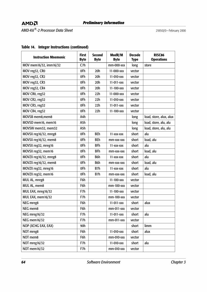
64 Software Environment Chapter 3
AMD-K6®-2 Processor Data Sheet 21850J/0—February 2000
Preliminary Information
MOV mem16/32, imm16/32 C7h mm-000-xxx long store
MOV reg32, CR0 0Fh 20h 11-000-xxx vector
MOV reg32, CR2 0Fh 20h 11-010-xxx vector
MOV reg32, CR3 0Fh 20h 11-011-xxx vector
MOV reg32, CR4 0Fh 20h 11-100-xxx vector
MOV CR0, reg32 0Fh 22h 11-000-xxx vector
MOV CR2, reg32 0Fh 22h 11-010-xxx vector
MOV CR3, reg32 0Fh 22h 11-011-xxx vector
MOV CR4, reg32 0Fh 22h 11-100-xxx vector
MOVSB mem8,mem8 A4h long load, store, alux, alux
MOVSD mem16, mem16 A5h long load, store, alu, alu
MOVSW mem32, mem32 A5h long load, store, alu, alu
MOVSX reg16/32, mreg8 0Fh BEh 11-xxx-xxx short alu
MOVSX reg16/32, mem8 0Fh BEh mm-xxx-xxx short load, alu
MOVSX reg32, mreg16 0Fh BFh 11-xxx-xxx short alu
MOVSX reg32, mem16 0Fh BFh mm-xxx-xxx short load, alu
MOVZX reg16/32, mreg8 0Fh B6h 11-xxx-xxx short alu
MOVZX reg16/32, mem8 0Fh B6h mm-xxx-xxx short load, alu
MOVZX reg32, mreg16 0Fh B7h 11-xxx-xxx short alu
MOVZX reg32, mem16 0Fh B7h mm-xxx-xxx short load, alu
MUL AL, mreg8 F6h 11-100-xxx vector
MUL AL, mem8 F6h mm-100-xxx vector
MUL EAX, mreg16/32 F7h 11-100-xxx vector
MUL EAX, mem16/32 F7h mm-100-xxx vector
NEG mreg8 F6h 11-011-xxx short alux
NEG mem8 F6h mm-011-xxx vector
NEG mreg16/32 F7h 11-011-xxx short alu
NEG mem16/32 F7h mm-011-xxx vector
NOP (XCHG EAX, EAX) 90h short limm
NOT mreg8 F6h 11-010-xxx short alux
NOT mem8 F6h mm-010-xxx vector
NOT mreg16/32 F7h 11-010-xxx short alu
NOT mem16/32 F7h mm-010-xxx vector
Table 14. Integer Instructions (continued)
Instruction MnemonicFirst Byte
Second Byte
ModR/M Byte
DecodeType
RISC86Operations

Chapter 3 Software Environment 65
21850J/0—February 2000 AMD-K6®-2 Processor Data Sheet
Preliminary Information
OR mreg8, reg8 08h 11-xxx-xxx short alux
OR mem8, reg8 08h mm-xxx-xxx long load, alux, store
OR mreg16/32, reg16/32 09h 11-xxx-xxx short alu
OR mem16/32, reg16/32 09h mm-xxx-xxx long load, alu, store
OR reg8, mreg8 0Ah 11-xxx-xxx short alux
OR reg8, mem8 0Ah mm-xxx-xxx short load, alux
OR reg16/32, mreg16/32 0Bh 11-xxx-xxx short alu
OR reg16/32, mem16/32 0Bh mm-xxx-xxx short load, alu
OR AL, imm8 0Ch short alux
OR EAX, imm16/32 0Dh short alu
OR mreg8, imm8 80h 11-001-xxx short alux
OR mem8, imm8 80h mm-001-xxx long load, alux, store
OR mreg16/32, imm16/32 81h 11-001-xxx short alu
OR mem16/32, imm16/32 81h mm-001-xxx long load, alu, store
OR mreg16/32, imm8 (signed ext.) 83h 11-001-xxx short alux
OR mem16/32, imm8 (signed ext.) 83h mm-001-xxx long load, alux, store
OUT imm8, AL E6h vector
OUT imm8, AX E7h vector
OUT imm8, EAX E7h vector
OUT DX, AL EEh vector
OUT DX, AX EFh vector
OUT DX, EAX EFh vector
POP ES 07h vector
POP SS 17h vector
POP DS 1Fh vector
POP FS 0Fh A1h vector
POP GS 0Fh A9h vector
POP EAX 58h short load, alu
POP ECX 59h short load, alu
POP EDX 5Ah short load, alu
POP EBX 5Bh short load, alu
POP ESP 5Ch short load, alu
POP EBP 5Dh short load, alu
Table 14. Integer Instructions (continued)
Instruction MnemonicFirst Byte
Second Byte
ModR/M Byte
DecodeType
RISC86Operations

66 Software Environment Chapter 3
AMD-K6®-2 Processor Data Sheet 21850J/0—February 2000
Preliminary Information
POP ESI 5Eh short load, alu
POP EDI 5Fh short load, alu
POP mreg 16/32 8Fh 11-000-xxx short load, alu
POP mem 16/32 8Fh mm-000-xxx long load, store, alu
POPA/POPAD 61h vector
POPF/POPFD 9Dh vector
PUSH ES 06h long load, store
PUSH CS 0Eh vector
PUSH FS 0Fh A0h vector
PUSH GS 0Fh A8h vector
PUSH SS 16h vector
PUSH DS 1Eh long load, store
PUSH EAX 50h short store
PUSH ECX 51h short store
PUSH EDX 52h short store
PUSH EBX 53h short store
PUSH ESP 54h short store
PUSH EBP 55h short store
PUSH ESI 56h short store
PUSH EDI 57h short store
PUSH imm8 6Ah long store
PUSH imm16/32 68h long store
PUSH mreg16/32 FFh 11-110-xxx vector
PUSH mem16/32 FFh mm-110-xxx long load, store
PUSHA/PUSHAD 60h vector
PUSHF/PUSHFD 9Ch vector
RCL mreg8, imm8 C0h 11-010-xxx vector
RCL mem8, imm8 C0h mm-010-xxx vector
RCL mreg16/32, imm8 C1h 11-010-xxx vector
RCL mem16/32, imm8 C1h mm-010-xxx vector
RCL mreg8, 1 D0h 11-010-xxx vector
RCL mem8, 1 D0h mm-010-xxx vector
RCL mreg16/32, 1 D1h 11-010-xxx vector
Table 14. Integer Instructions (continued)
Instruction MnemonicFirst Byte
Second Byte
ModR/M Byte
DecodeType
RISC86Operations
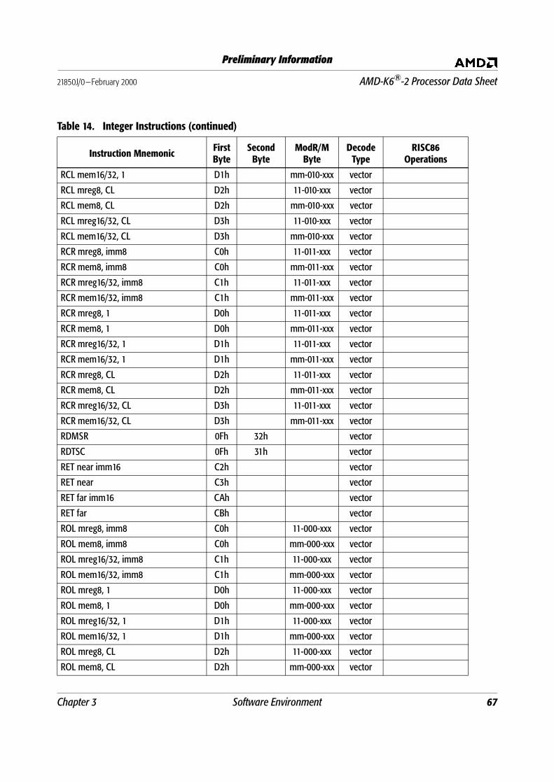
Chapter 3 Software Environment 67
21850J/0—February 2000 AMD-K6®-2 Processor Data Sheet
Preliminary Information
RCL mem16/32, 1 D1h mm-010-xxx vector
RCL mreg8, CL D2h 11-010-xxx vector
RCL mem8, CL D2h mm-010-xxx vector
RCL mreg16/32, CL D3h 11-010-xxx vector
RCL mem16/32, CL D3h mm-010-xxx vector
RCR mreg8, imm8 C0h 11-011-xxx vector
RCR mem8, imm8 C0h mm-011-xxx vector
RCR mreg16/32, imm8 C1h 11-011-xxx vector
RCR mem16/32, imm8 C1h mm-011-xxx vector
RCR mreg8, 1 D0h 11-011-xxx vector
RCR mem8, 1 D0h mm-011-xxx vector
RCR mreg16/32, 1 D1h 11-011-xxx vector
RCR mem16/32, 1 D1h mm-011-xxx vector
RCR mreg8, CL D2h 11-011-xxx vector
RCR mem8, CL D2h mm-011-xxx vector
RCR mreg16/32, CL D3h 11-011-xxx vector
RCR mem16/32, CL D3h mm-011-xxx vector
RDMSR 0Fh 32h vector
RDTSC 0Fh 31h vector
RET near imm16 C2h vector
RET near C3h vector
RET far imm16 CAh vector
RET far CBh vector
ROL mreg8, imm8 C0h 11-000-xxx vector
ROL mem8, imm8 C0h mm-000-xxx vector
ROL mreg16/32, imm8 C1h 11-000-xxx vector
ROL mem16/32, imm8 C1h mm-000-xxx vector
ROL mreg8, 1 D0h 11-000-xxx vector
ROL mem8, 1 D0h mm-000-xxx vector
ROL mreg16/32, 1 D1h 11-000-xxx vector
ROL mem16/32, 1 D1h mm-000-xxx vector
ROL mreg8, CL D2h 11-000-xxx vector
ROL mem8, CL D2h mm-000-xxx vector
Table 14. Integer Instructions (continued)
Instruction MnemonicFirst Byte
Second Byte
ModR/M Byte
DecodeType
RISC86Operations

68 Software Environment Chapter 3
AMD-K6®-2 Processor Data Sheet 21850J/0—February 2000
Preliminary Information
ROL mreg16/32, CL D3h 11-000-xxx vector
ROL mem16/32, CL D3h mm-000-xxx vector
ROR mreg8, imm8 C0h 11-001-xxx vector
ROR mem8, imm8 C0h mm-001-xxx vector
ROR mreg16/32, imm8 C1h 11-001-xxx vector
ROR mem16/32, imm8 C1h mm-001-xxx vector
ROR mreg8, 1 D0h 11-001-xxx vector
ROR mem8, 1 D0h mm-001-xxx vector
ROR mreg16/32, 1 D1h 11-001-xxx vector
ROR mem16/32, 1 D1h mm-001-xxx vector
ROR mreg8, CL D2h 11-001-xxx vector
ROR mem8, CL D2h mm-001-xxx vector
ROR mreg16/32, CL D3h 11-001-xxx vector
ROR mem16/32, CL D3h mm-001-xxx vector
RSM 0Fh AAh vector
SAHF 9Eh vector
SAR mreg8, imm8 C0h 11-111-xxx short alux
SAR mem8, imm8 C0h mm-111-xxx vector
SAR mreg16/32, imm8 C1h 11-111-xxx short alu
SAR mem16/32, imm8 C1h mm-111-xxx vector
SAR mreg8, 1 D0h 11-111-xxx short alux
SAR mem8, 1 D0h mm-111-xxx vector
SAR mreg16/32, 1 D1h 11-111-xxx short alu
SAR mem16/32, 1 D1h mm-111-xxx vector
SAR mreg8, CL D2h 11-111-xxx short alux
SAR mem8, CL D2h mm-111-xxx vector
SAR mreg16/32, CL D3h 11-111-xxx short alu
SAR mem16/32, CL D3h mm-111-xxx vector
SBB mreg8, reg8 18h 11-xxx-xxx vector
SBB mem8, reg8 18h mm-xxx-xxx vector
SBB mreg16/32, reg16/32 19h 11-xxx-xxx vector
SBB mem16/32, reg16/32 19h mm-xxx-xxx vector
SBB reg8, mreg8 1Ah 11-xxx-xxx vector
Table 14. Integer Instructions (continued)
Instruction MnemonicFirst Byte
Second Byte
ModR/M Byte
DecodeType
RISC86Operations

Chapter 3 Software Environment 69
21850J/0—February 2000 AMD-K6®-2 Processor Data Sheet
Preliminary Information
SBB reg8, mem8 1Ah mm-xxx-xxx vector
SBB reg16/32, mreg16/32 1Bh 11-xxx-xxx vector
SBB reg16/32, mem16/32 1Bh mm-xxx-xxx vector
SBB AL, imm8 1Ch vector
SBB EAX, imm16/32 1Dh vector
SBB mreg8, imm8 80h 11-011-xxx vector
SBB mem8, imm8 80h mm-011-xxx vector
SBB mreg16/32, imm16/32 81h 11-011-xxx vector
SBB mem16/32, imm16/32 81h mm-011-xxx vector
SBB mreg16/32, imm8 (signed ext.) 83h 11-011-xxx vector
SBB mem16/32, imm8 (signed ext.) 83h mm-011-xxx vector
SCASB AL, mem8 AEh vector
SCASW AX, mem16 AFh vector
SCASD EAX, mem32 AFh vector
SETO mreg8 0Fh 90h 11-xxx-xxx vector
SETO mem8 0Fh 90h mm-xxx-xxx vector
SETNO mreg8 0Fh 91h 11-xxx-xxx vector
SETNO mem8 0Fh 91h mm-xxx-xxx vector
SETB/SETNAE mreg8 0Fh 92h 11-xxx-xxx vector
SETB/SETNAE mem8 0Fh 92h mm-xxx-xxx vector
SETNB/SETAE mreg8 0Fh 93h 11-xxx-xxx vector
SETNB/SETAE mem8 0Fh 93h mm-xxx-xxx vector
SETZ/SETE mreg8 0Fh 94h 11-xxx-xxx vector
SETZ/SETE mem8 0Fh 94h mm-xxx-xxx vector
SETNZ/SETNE mreg8 0Fh 95h 11-xxx-xxx vector
SETNZ/SETNE mem8 0Fh 95h mm-xxx-xxx vector
SETBE/SETNA mreg8 0Fh 96h 11-xxx-xxx vector
SETBE/SETNA mem8 0Fh 96h mm-xxx-xxx vector
SETNBE/SETA mreg8 0Fh 97h 11-xxx-xxx vector
SETNBE/SETA mem8 0Fh 97h mm-xxx-xxx vector
SETS mreg8 0Fh 98h 11-xxx-xxx vector
SETS mem8 0Fh 98h mm-xxx-xxx vector
SETNS mreg8 0Fh 99h 11-xxx-xxx vector
Table 14. Integer Instructions (continued)
Instruction MnemonicFirst Byte
Second Byte
ModR/M Byte
DecodeType
RISC86Operations

70 Software Environment Chapter 3
AMD-K6®-2 Processor Data Sheet 21850J/0—February 2000
Preliminary Information
SETNS mem8 0Fh 99h mm-xxx-xxx vector
SETP/SETPE mreg8 0Fh 9Ah 11-xxx-xxx vector
SETP/SETPE mem8 0Fh 9Ah mm-xxx-xxx vector
SETNP/SETPO mreg8 0Fh 9Bh 11-xxx-xxx vector
SETNP/SETPO mem8 0Fh 9Bh mm-xxx-xxx vector
SETL/SETNGE mreg8 0Fh 9Ch 11-xxx-xxx vector
SETL/SETNGE mem8 0Fh 9Ch mm-xxx-xxx vector
SETNL/SETGE mreg8 0Fh 9Dh 11-xxx-xxx vector
SETNL/SETGE mem8 0Fh 9Dh mm-xxx-xxx vector
SETLE/SETNG mreg8 0Fh 9Eh 11-xxx-xxx vector
SETLE/SETNG mem8 0Fh 9Eh mm-xxx-xxx vector
SETNLE/SETG mreg8 0Fh 9Fh 11-xxx-xxx vector
SETNLE/SETG mem8 0Fh 9Fh mm-xxx-xxx vector
SGDT mem48 0Fh 01h mm-000-xxx vector
SIDT mem48 0Fh 01h mm-001-xxx vector
SHL/SAL mreg8, imm8 C0h 11-100-xxx short alux
SHL/SAL mem8, imm8 C0h mm-100-xxx vector
SHL/SAL mreg16/32, imm8 C1h 11-100-xxx short alu
SHL/SAL mem16/32, imm8 C1h mm-100-xxx vector
SHL/SAL mreg8, 1 D0h 11-100-xxx short alux
SHL/SAL mem8, 1 D0h mm-100-xxx vector
SHL/SAL mreg16/32, 1 D1h 11-100-xxx short alu
SHL/SAL mem16/32, 1 D1h mm-100-xxx vector
SHL/SAL mreg8, CL D2h 11-100-xxx short alux
SHL/SAL mem8, CL D2h mm-100-xxx vector
SHL/SAL mreg16/32, CL D3h 11-100-xxx short alu
SHL/SAL mem16/32, CL D3h mm-100-xxx vector
SHR mreg8, imm8 C0h 11-101-xxx short alux
SHR mem8, imm8 C0h mm-101-xxx vector
SHR mreg16/32, imm8 C1h 11-101-xxx short alu
SHR mem16/32, imm8 C1h mm-101-xxx vector
SHR mreg8, 1 D0h 11-101-xxx short alux
SHR mem8, 1 D0h mm-101-xxx vector
Table 14. Integer Instructions (continued)
Instruction MnemonicFirst Byte
Second Byte
ModR/M Byte
DecodeType
RISC86Operations

Chapter 3 Software Environment 71
21850J/0—February 2000 AMD-K6®-2 Processor Data Sheet
Preliminary Information
SHR mreg16/32, 1 D1h 11-101-xxx short alu
SHR mem16/32, 1 D1h mm-101-xxx vector
SHR mreg8, CL D2h 11-101-xxx short alux
SHR mem8, CL D2h mm-101-xxx vector
SHR mreg16/32, CL D3h 11-101-xxx short alu
SHR mem16/32, CL D3h mm-101-xxx vector
SHLD mreg16/32, reg16/32, imm8 0Fh A4h 11-xxx-xxx vector
SHLD mem16/32, reg16/32, imm8 0Fh A4h mm-xxx-xxx vector
SHLD mreg16/32, reg16/32, CL 0Fh A5h 11-xxx-xxx vector
SHLD mem16/32, reg16/32, CL 0Fh A5h mm-xxx-xxx vector
SHRD mreg16/32, reg16/32, imm8 0Fh ACh 11-xxx-xxx vector
SHRD mem16/32, reg16/32, imm8 0Fh ACh mm-xxx-xxx vector
SHRD mreg16/32, reg16/32, CL 0Fh ADh 11-xxx-xxx vector
SHRD mem16/32, reg16/32, CL 0Fh ADh mm-xxx-xxx vector
SLDT mreg16 0Fh 00h 11-000-xxx vector
SLDT mem16 0Fh 00h mm-000-xxx vector
SMSW mreg16 0Fh 01h 11-100-xxx vector
SMSW mem16 0Fh 01h mm-100-xxx vector
STC F9h vector
STD FDh vector
STI FBh vector
STOSB mem8, AL AAh long store, alux
STOSW mem16, AX ABh long store, alux
STOSD mem32, EAX ABh long store, alux
STR mreg16 0Fh 00h 11-001-xxx vector
STR mem16 0Fh 00h mm-001-xxx vector
SUB mreg8, reg8 28h 11-xxx-xxx short alux
SUB mem8, reg8 28h mm-xxx-xxx long load, alux, store
SUB mreg16/32, reg16/32 29h 11-xxx-xxx short alu
SUB mem16/32, reg16/32 29h mm-xxx-xxx long load, alu, store
SUB reg8, mreg8 2Ah 11-xxx-xxx short alux
SUB reg8, mem8 2Ah mm-xxx-xxx short load, alux
SUB reg16/32, mreg16/32 2Bh 11-xxx-xxx short alu
Table 14. Integer Instructions (continued)
Instruction MnemonicFirst Byte
Second Byte
ModR/M Byte
DecodeType
RISC86Operations

72 Software Environment Chapter 3
AMD-K6®-2 Processor Data Sheet 21850J/0—February 2000
Preliminary Information
SUB reg16/32, mem16/32 2Bh mm-xxx-xxx short load, alu
SUB AL, imm8 2Ch short alux
SUB EAX, imm16/32 2Dh short alu
SUB mreg8, imm8 80h 11-101-xxx short alux
SUB mem8, imm8 80h mm-101-xxx long load, alux, store
SUB mreg16/32, imm16/32 81h 11-101-xxx short alu
SUB mem16/32, imm16/32 81h mm-101-xxx long load, alu, store
SUB mreg16/32, imm8 (signed ext.) 83h 11-101-xxx short alux
SUB mem16/32, imm8 (signed ext.) 83h mm-101-xxx long load, alux, store
SYSCALL 0Fh 05h vector
SYSRET 0Fh 07h vector
TEST mreg8, reg8 84h 11-xxx-xxx short alux
TEST mem8, reg8 84h mm-xxx-xxx vector
TEST mreg16/32, reg16/32 85h 11-xxx-xxx short alu
TEST mem16/32, reg16/32 85h mm-xxx-xxx vector
TEST AL, imm8 A8h long alux
TEST EAX, imm16/32 A9h long alu
TEST mreg8, imm8 F6h 11-000-xxx long alux
TEST mem8, imm8 F6h mm-000-xxx long load, alux
TEST mreg16/32, imm16/32 F7h 11-000-xxx long alu
TEST mem16/32, imm16/32 F7h mm-000-xxx long load, alu
VERR mreg16 0Fh 00h 11-100-xxx vector
VERR mem16 0Fh 00h mm-100-xxx vector
VERW mreg16 0Fh 00h 11-101-xxx vector
VERW mem16 0Fh 00h mm-101-xxx vector
WAIT 9Bh vector
WBINVD 0Fh 09h vector
WRMSR 0Fh 30h vector
XADD mreg8, reg8 0Fh C0h 11-100-xxx vector
XADD mem8, reg8 0Fh C0h mm-100-xxx vector
XADD mreg16/32, reg16/32 0Fh C1h 11-101-xxx vector
XADD mem16/32, reg16/32 0Fh C1h mm-101-xxx vector
XCHG reg8, mreg8 86h 11-xxx-xxx vector
Table 14. Integer Instructions (continued)
Instruction MnemonicFirst Byte
Second Byte
ModR/M Byte
DecodeType
RISC86Operations
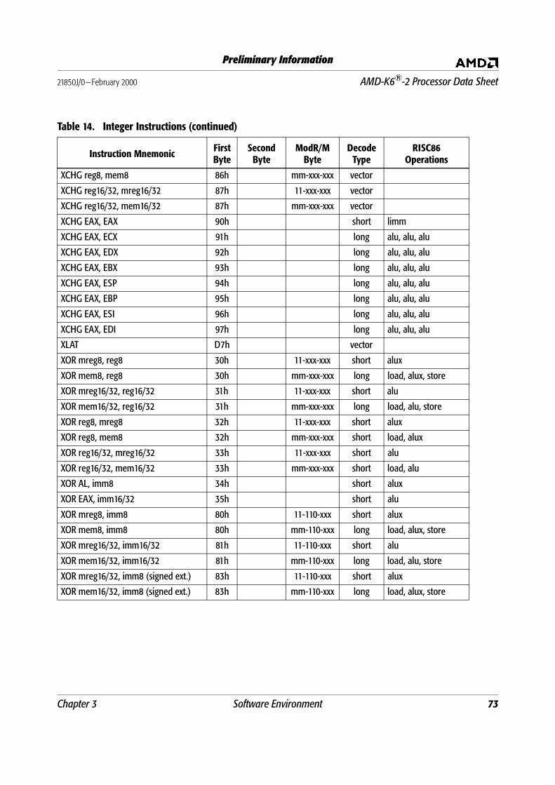
Chapter 3 Software Environment 73
21850J/0—February 2000 AMD-K6®-2 Processor Data Sheet
Preliminary Information
XCHG reg8, mem8 86h mm-xxx-xxx vector
XCHG reg16/32, mreg16/32 87h 11-xxx-xxx vector
XCHG reg16/32, mem16/32 87h mm-xxx-xxx vector
XCHG EAX, EAX 90h short limm
XCHG EAX, ECX 91h long alu, alu, alu
XCHG EAX, EDX 92h long alu, alu, alu
XCHG EAX, EBX 93h long alu, alu, alu
XCHG EAX, ESP 94h long alu, alu, alu
XCHG EAX, EBP 95h long alu, alu, alu
XCHG EAX, ESI 96h long alu, alu, alu
XCHG EAX, EDI 97h long alu, alu, alu
XLAT D7h vector
XOR mreg8, reg8 30h 11-xxx-xxx short alux
XOR mem8, reg8 30h mm-xxx-xxx long load, alux, store
XOR mreg16/32, reg16/32 31h 11-xxx-xxx short alu
XOR mem16/32, reg16/32 31h mm-xxx-xxx long load, alu, store
XOR reg8, mreg8 32h 11-xxx-xxx short alux
XOR reg8, mem8 32h mm-xxx-xxx short load, alux
XOR reg16/32, mreg16/32 33h 11-xxx-xxx short alu
XOR reg16/32, mem16/32 33h mm-xxx-xxx short load, alu
XOR AL, imm8 34h short alux
XOR EAX, imm16/32 35h short alu
XOR mreg8, imm8 80h 11-110-xxx short alux
XOR mem8, imm8 80h mm-110-xxx long load, alux, store
XOR mreg16/32, imm16/32 81h 11-110-xxx short alu
XOR mem16/32, imm16/32 81h mm-110-xxx long load, alu, store
XOR mreg16/32, imm8 (signed ext.) 83h 11-110-xxx short alux
XOR mem16/32, imm8 (signed ext.) 83h mm-110-xxx long load, alux, store
Table 14. Integer Instructions (continued)
Instruction MnemonicFirst Byte
Second Byte
ModR/M Byte
DecodeType
RISC86Operations

74 Software Environment Chapter 3
AMD-K6®-2 Processor Data Sheet 21850J/0—February 2000
Preliminary Information
Table 15. Floating-Point Instructions
Instruction MnemonicFirst Byte
Second Byte
ModR/M Byte
DecodeType
RISC86Operations
Note
F2XM1 D9h F0h short float
FABS D9h F1h short float
FADD ST(0), ST(i) D8h 11-000-xxx short float *
FADD ST(0), mem32real D8h mm-000-xxx short fload, float
FADD ST(i), ST(0) DCh 11-000-xxx short float *
FADD ST(0), mem64real DCh mm-000-xxx short fload, float
FADDP ST(i), ST(0) DEh 11-000-xxx short float *
FBLD DFh mm-100-xxx vector
FBSTP DFh mm-110-xxx vector
FCHS D9h E0h short float
FCLEX DBh E2h vector
FCOM ST(0), ST(i) D8h 11-010-xxx short float *
FCOM ST(0), mem32real D8h mm-010-xxx short fload, float
FCOM ST(0), mem64real DCh mm-010-xxx short fload, float
FCOMP ST(0), ST(i) D8h 11-011-xxx short float *
FCOMP ST(0), mem32real D8h mm-011-xxx short fload, float
FCOMP ST(0), mem64real DCh mm-011-xxx short fload, float
FCOMPP DEh D9h 11-011-001 short float
FCOS D9h FFh short float
FDECSTP D9h F6h short float
FDIV ST(0), ST(i) (single precision) D8h 11-110-xxx short float *
FDIV ST(0), ST(i) (double precision) D8h 11-110-xxx short float *
FDIV ST(0), ST(i) (extended precision) D8h 11-110-xxx short float *
FDIV ST(i), ST(0) (single precision) DCh 11-111-xxx short float *
FDIV ST(i), ST(0) (double precision) DCh 11-111-xxx short float *
FDIV ST(i), ST(0) (extended precision) DCh 11-111-xxx short float *
FDIV ST(0), mem32real D8h mm-110-xxx short fload, float
FDIV ST(0), mem64real DCh mm-110-xxx short fload, float
FDIVP ST(0), ST(i) DEh 11-111-xxx short float *
FDIVR ST(0), ST(i) D8h 11-110-xxx short float *
FDIVR ST(i), ST(0) DCh 11-111-xxx short float *
Note:
* The last three bits of the modR/M byte select the stack entry ST(i).

Chapter 3 Software Environment 75
21850J/0—February 2000 AMD-K6®-2 Processor Data Sheet
Preliminary Information
FDIVR ST(0), mem32real D8h mm-111-xxx short fload, float
FDIVR ST(0), mem64real DCh mm-111-xxx short fload, float
FDIVRP ST(i), ST(0) DEh 11-110-xxx short float *
FFREE ST(i) DDh 11-000-xxx short float *
FIADD ST(0), mem32int DAh mm-000-xxx short fload, float
FIADD ST(0), mem16int DEh mm-000-xxx short fload, float
FICOM ST(0), mem32int DAh mm-010-xxx short fload, float
FICOM ST(0), mem16int DEh mm-010-xxx short fload, float
FICOMP ST(0), mem32int DAh mm-011-xxx short fload, float
FICOMP ST(0), mem16int DEh mm-011-xxx short fload, float
FIDIV ST(0), mem32int DAh mm-110-xxx short fload, float
FIDIV ST(0), mem16int DEh mm-110-xxx short fload, float
FIDIVR ST(0), mem32int DAh mm-111-xxx short fload, float
FIDIVR ST(0), mem16int DEh mm-111-xxx short fload, float
FILD mem16int DFh mm-000-xxx short fload, float
FILD mem32int DBh mm-000-xxx short fload, float
FILD mem64int DFh mm-101-xxx short fload, float
FIMUL ST(0), mem32int DAh mm-001-xxx short fload, float
FIMUL ST(0), mem16int DEh mm-001-xxx short fload, float
FINCSTP D9h F7h short
FINIT DBh E3h vector
FIST mem16int DFh mm-010-xxx short fload, float
FIST mem32int DBh mm-010-xxx short fload, float
FISTP mem16int DFh mm-011-xxx short fload, float
FISTP mem32int DBh mm-011-xxx short fload, float
FISTP mem64int DFh mm-111-xxx short fload, float
FISUB ST(0), mem32int DAh mm-100-xxx short fload, float
FISUB ST(0), mem16int DEh mm-100-xxx short fload, float
FISUBR ST(0), mem32int DAh mm-101-xxx short fload, float
FISUBR ST(0), mem16int DEh mm-101-xxx short fload, float
FLD ST(i) D9h 11-000-xxx short fload, float *
Table 15. Floating-Point Instructions (continued)
Instruction MnemonicFirst Byte
Second Byte
ModR/M Byte
DecodeType
RISC86Operations
Note
Note:
* The last three bits of the modR/M byte select the stack entry ST(i).

76 Software Environment Chapter 3
AMD-K6®-2 Processor Data Sheet 21850J/0—February 2000
Preliminary Information
FLD mem32real D9h mm-000-xxx short fload, float
FLD mem64real DDh mm-000-xxx short fload, float
FLD mem80real DBh mm-101-xxx vector
FLD1 D9h E8h short fload, float
FLDCW D9h mm-101-xxx vector
FLDENV D9h mm-100-xxx short fload, float
FLDL2E D9h EAh short float
FLDL2T D9h E9h short float
FLDLG2 D9h ECh short float
FLDLN2 D9h EDh short float
FLDPI D9h EBh short float
FLDZ D9h EEh short float
FMUL ST(0), ST(i) D8h 11-001-xxx short float *
FMUL ST(i), ST(0) DCh 11-001-xxx short float *
FMUL ST(0), mem32real D8h mm-001-xxx short fload, float
FMUL ST(0), mem64real DCh mm-001-xxx short fload, float
FMULP ST(0), ST(i) DEh 11-001-xxx short float *
FNOP D9h D0h short float
FPATAN D9h F3h short float
FPREM D9h F8h short float
FPREM1 D9h F5h short float
FPTAN D9h F2h vector
FRNDINT D9h FCh short float
FRSTOR DDh mm-100-xxx vector
FSAVE DDh mm-110-xxx vector
FSCALE D9h FDh short float
FSIN D9h FEh short float
FSINCOS D9h FBh vector
FSQRT (single precision) D9h FAh short float
FSQRT (double precision) D9h FAh short float
FSQRT (extended precision) D9h FAh short float
Table 15. Floating-Point Instructions (continued)
Instruction MnemonicFirst Byte
Second Byte
ModR/M Byte
DecodeType
RISC86Operations
Note
Note:
* The last three bits of the modR/M byte select the stack entry ST(i).

Chapter 3 Software Environment 77
21850J/0—February 2000 AMD-K6®-2 Processor Data Sheet
Preliminary Information
FST mem32real D9h mm-010-xxx short fstore
FST mem64real DDh mm-010-xxx short fstore
FST ST(i) DDh 11-010-xxx short fstore *
FSTCW D9h mm-111-xxx vector
FSTENV D9h mm-110-xxx vector
FSTP mem32real D9h mm-011-xxx short fstore
FSTP mem64real DDh mm-011-xxx short fstore
FSTP mem80real D9h mm-111-xxx vector
FSTP ST(i) DDh 11-011-xxx short float *
FSTSW AX DFh E0h vector
FSTSW mem16 DDh mm-111-xxx vector
FSUB ST(0), mem32real D8h mm-100-xxx short fload, float
FSUB ST(0), mem64real DCh mm-100-xxx short fload, float
FSUB ST(0), ST(i) D8h 11-100-xxx short float *
FSUB ST(i), ST(0) DCh 11-101-xxx short float *
FSUBP ST(0), ST(i) DEh 11-101-xxx short float *
FSUBR ST(0), mem32real D8h mm-101-xxx short fload, float
FSUBR ST(0), mem64real DCh mm-101-xxx short fload, float
FSUBR ST(0), ST(i) D8h 11-100-xxx short float *
FSUBR ST(i), ST(0) DCh 11-101-xxx short float *
FSUBRP ST(i), ST(0) DEh 11-100-xxx short float *
FTST D9h E4h short float
FUCOM DDh 11-100-xxx short float
FUCOMP DDh 11-101-xxx short float
FUCOMPP DAh E9h short float
FXAM D9h E5h short float
FXCH D9h 11-001-xxx short float
FXTRACT D9h F4h vector
FYL2X D9h F1h short float
FYL2XP1 D9h F9h short float
FWAIT 9Bh vector
Table 15. Floating-Point Instructions (continued)
Instruction MnemonicFirst Byte
Second Byte
ModR/M Byte
DecodeType
RISC86Operations
Note
Note:
* The last three bits of the modR/M byte select the stack entry ST(i).

78 Software Environment Chapter 3
AMD-K6®-2 Processor Data Sheet 21850J/0—February 2000
Preliminary Information
Table 16. MMX™ Instructions
Instruction MnemonicPrefixByte(s)
FirstByte
ModR/M Byte
DecodeType
RISC86Operations
Note
EMMS 0Fh 77h vector
MOVD mmreg, mreg32 0Fh 6Eh 11-xxx-xxx short meu **
MOVD mmreg, mem32 0Fh 6Eh mm-xxx-xxx short mload
MOVD mreg32, mmreg 0Fh 7Eh 11-xxx-xxx short mstore, load **
MOVD mem32, mmreg 0Fh 7Eh mm-xxx-xxx short mstore
MOVQ mmreg1, mmreg2 0Fh 6Fh 11-xxx-xxx short meu
MOVQ mmreg, mem64 0Fh 6Fh mm-xxx-xxx short mload
MOVQ mmreg2, mmreg1 0Fh 7Fh 11-xxx-xxx short meu
MOVQ mem64, mmreg 0Fh 7Fh mm-xxx-xxx short mstore
PACKSSDW mmreg1, mmreg2 0Fh 6Bh 11-xxx-xxx short meu
PACKSSDW mmreg, mem64 0Fh 6Bh mm-xxx-xxx short mload, meu
PACKSSWB mmreg1, mmreg2 0Fh 63h 11-xxx-xxx short meu
PACKSSWB mmreg, mem64 0Fh 63h mm-xxx-xxx short mload, meu
PACKUSWB mmreg1, mmreg2 0Fh 67h 11-xxx-xxx short meu
PACKUSWB mmreg, mem64 0Fh 67h mm-xxx-xxx short mload, meu
PADDB mmreg1, mmreg2 0Fh FCh 11-xxx-xxx short meu
PADDB mmreg, mem64 0Fh FCh mm-xxx-xxx short mload, meu
PADDD mmreg1, mmreg2 0Fh FEh 11-xxx-xxx short meu
PADDD mmreg, mem64 0Fh FEh mm-xxx-xxx short mload, meu
PADDSB mmreg1, mmreg2 0Fh ECh 11-xxx-xxx short meu
PADDSB mmreg, mem64 0Fh ECh mm-xxx-xxx short mload, meu
PADDSW mmreg1, mmreg2 0Fh EDh 11-xxx-xxx short meu
PADDSW mmreg, mem64 0Fh EDh mm-xxx-xxx short mload, meu
PADDUSB mmreg1, mmreg2 0Fh DCh 11-xxx-xxx short meu
PADDUSB mmreg, mem64 0Fh DCh mm-xxx-xxx short mload, meu
PADDUSW mmreg1, mmreg2 0Fh DDh 11-xxx-xxx short meu
PADDUSW mmreg, mem64 0Fh DDh mm-xxx-xxx short mload, meu
PADDW mmreg1, mmreg2 0Fh FDh 11-xxx-xxx short meu
PADDW mmreg, mem64 0Fh FDh mm-xxx-xxx short mload, meu
PAND mmreg1, mmreg2 0Fh DBh 11-xxx-xxx short meu
PAND mmreg, mem64 0Fh DBh mm-xxx-xxx short mload, meu
Note:
** Bits 2, 1, and 0 of the modR/M byte select the integer register.
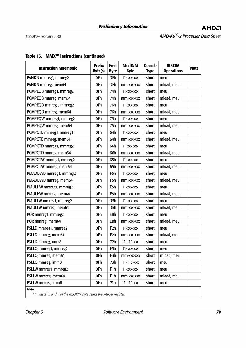
Chapter 3 Software Environment 79
21850J/0—February 2000 AMD-K6®-2 Processor Data Sheet
Preliminary Information
PANDN mmreg1, mmreg2 0Fh DFh 11-xxx-xxx short meu
PANDN mmreg, mem64 0Fh DFh mm-xxx-xxx short mload, meu
PCMPEQB mmreg1, mmreg2 0Fh 74h 11-xxx-xxx short meu
PCMPEQB mmreg, mem64 0Fh 74h mm-xxx-xxx short mload, meu
PCMPEQD mmreg1, mmreg2 0Fh 76h 11-xxx-xxx short meu
PCMPEQD mmreg, mem64 0Fh 76h mm-xxx-xxx short mload, meu
PCMPEQW mmreg1, mmreg2 0Fh 75h 11-xxx-xxx short meu
PCMPEQW mmreg, mem64 0Fh 75h mm-xxx-xxx short mload, meu
PCMPGTB mmreg1, mmreg2 0Fh 64h 11-xxx-xxx short meu
PCMPGTB mmreg, mem64 0Fh 64h mm-xxx-xxx short mload, meu
PCMPGTD mmreg1, mmreg2 0Fh 66h 11-xxx-xxx short meu
PCMPGTD mmreg, mem64 0Fh 66h mm-xxx-xxx short mload, meu
PCMPGTW mmreg1, mmreg2 0Fh 65h 11-xxx-xxx short meu
PCMPGTW mmreg, mem64 0Fh 65h mm-xxx-xxx short mload, meu
PMADDWD mmreg1, mmreg2 0Fh F5h 11-xxx-xxx short meu
PMADDWD mmreg, mem64 0Fh F5h mm-xxx-xxx short mload, meu
PMULHW mmreg1, mmreg2 0Fh E5h 11-xxx-xxx short meu
PMULHW mmreg, mem64 0Fh E5h mm-xxx-xxx short mload, meu
PMULLW mmreg1, mmreg2 0Fh D5h 11-xxx-xxx short meu
PMULLW mmreg, mem64 0Fh D5h mm-xxx-xxx short mload, meu
POR mmreg1, mmreg2 0Fh EBh 11-xxx-xxx short meu
POR mmreg, mem64 0Fh EBh mm-xxx-xxx short mload, meu
PSLLD mmreg1, mmreg2 0Fh F2h 11-xxx-xxx short meu
PSLLD mmreg, mem64 0Fh F2h mm-xxx-xxx short mload, meu
PSLLD mmreg, imm8 0Fh 72h 11-110-xxx short meu
PSLLQ mmreg1, mmreg2 0Fh F3h 11-xxx-xxx short meu
PSLLQ mmreg, mem64 0Fh F3h mm-xxx-xxx short mload, meu
PSLLQ mmreg, imm8 0Fh 73h 11-110-xxx short meu
PSLLW mmreg1, mmreg2 0Fh F1h 11-xxx-xxx short meu
PSLLW mmreg, mem64 0Fh F1h mm-xxx-xxx short mload, meu
PSLLW mmreg, imm8 0Fh 71h 11-110-xxx short meu
Table 16. MMX™ Instructions (continued)
Instruction MnemonicPrefixByte(s)
FirstByte
ModR/M Byte
DecodeType
RISC86Operations
Note
Note:
** Bits 2, 1, and 0 of the modR/M byte select the integer register.

80 Software Environment Chapter 3
AMD-K6®-2 Processor Data Sheet 21850J/0—February 2000
Preliminary Information
PSRAD mmreg1, mmreg2 0Fh E2h 11-xxx-xxx short meu
PSRAD mmreg, mem64 0Fh E2h mm-xxx-xxx short mload, meu
PSRAD mmreg, imm8 0Fh 72h 11-100-xxx short meu
PSRAW mmreg1, mmreg2 0Fh E1h 11-xxx-xxx short meu
PSRAW mmreg, mem64 0Fh E1h mm-xxx-xxx short mload, meu
PSRAW mmreg, imm8 0Fh 71h 11-100-xxx short meu
PSRLD mmreg1, mmreg2 0Fh D2h 11-xxx-xxx short meu
PSRLD mmreg, mem64 0Fh D2h mm-xxx-xxx short mload, meu
PSRLD mmreg, imm8 0Fh 72h 11-010-xxx short meu
PSRLQ mmreg1, mmreg2 0Fh D3h 11-xxx-xxx short meu
PSRLQ mmreg, mem64 0Fh D3h mm-xxx-xxx short mload, meu
PSRLQ mmreg, imm8 0Fh 73h 11-010-xxx short meu
PSRLW mmreg1, mmreg2 0Fh D1h 11-xxx-xxx short meu
PSRLW mmreg, mem64 0Fh D1h mm-xxx-xxx short mload, meu
PSRLW mmreg, imm8 0Fh 71h 11-010-xxx short meu
PSUBB mmreg1, mmreg2 0Fh F8h 11-xxx-xxx short meu
PSUBB mmreg, mem64 0Fh F8h mm-xxx-xxx short mload, meu
PSUBD mmreg1, mmreg2 0Fh FAh 11-xxx-xxx short meu
PSUBD mmreg, mem64 0Fh FAh mm-xxx-xxx short mload, meu
PSUBSB mmreg1, mmreg2 0Fh E8h 11-xxx-xxx short meu
PSUBSB mmreg, mem64 0Fh E8h mm-xxx-xxx short mload, meu
PSUBSW mmreg1, mmreg2 0Fh E9h 11-xxx-xxx short meu
PSUBSW mmreg, mem64 0Fh E9h mm-xxx-xxx short mload, meu
PSUBUSB mmreg1, mmreg2 0Fh D8h 11-xxx-xxx short meu
PSUBUSB mmreg, mem64 0Fh D8h mm-xxx-xxx short mload, meu
PSUBUSW mmreg1, mmreg2 0Fh D9h 11-xxx-xxx short meu
PSUBUSW mmreg, mem64 0Fh D9h mm-xxx-xxx short mload, meu
PSUBW mmreg1, mmreg2 0Fh F9h 11-xxx-xxx short meu
PSUBW mmreg, mem64 0Fh F9h mm-xxx-xxx short mload, meu
PUNPCKHBW mmreg1, mmreg2 0Fh 68h 11-xxx-xxx short meu
PUNPCKHBW mmreg, mem64 0Fh 68h mm-xxx-xxx short mload, meu
Table 16. MMX™ Instructions (continued)
Instruction MnemonicPrefixByte(s)
FirstByte
ModR/M Byte
DecodeType
RISC86Operations
Note
Note:
** Bits 2, 1, and 0 of the modR/M byte select the integer register.

Chapter 3 Software Environment 81
21850J/0—February 2000 AMD-K6®-2 Processor Data Sheet
Preliminary Information
PUNPCKHDQ mmreg1, mmreg2 0Fh 6Ah 11-xxx-xxx short meu
PUNPCKHDQ mmreg, mem64 0Fh 6Ah mm-xxx-xxx short mload, meu
PUNPCKHWD mmreg1, mmreg2 0Fh 69h 11-xxx-xxx short meu
PUNPCKHWD mmreg, mem64 0Fh 69h mm-xxx-xxx short mload, meu
PUNPCKLBW mmreg1, mmreg2 0Fh 60h 11-xxx-xxx short meu
PUNPCKLBW mmreg, mem32 0Fh 60h mm-xxx-xxx short mload, meu
PUNPCKLDQ mmreg1, mmreg2 0Fh 62h 11-xxx-xxx short meu
PUNPCKLDQ mmreg, mem32 0Fh 62h mm-xxx-xxx short mload, meu
PUNPCKLWD mmreg1, mmreg2 0Fh 61h 11-xxx-xxx short meu
PUNPCKLWD mmreg, mem32 0Fh 61h mm-xxx-xxx short mload, meu
PXOR mmreg1, mmreg2 0Fh EFh 11-xxx-xxx short meu
PXOR mmreg, mem64 0Fh EFh mm-xxx-xxx short mload, meu
Table 17. 3DNow!™ Instructions
Instruction MnemonicPrefixByte(s)
OpcodeByte
ModR/M Byte
DecodeType
RISC86Operations
Note
FEMMS 0Fh 0Eh vector
PAVGUSB mmreg1, mmreg2 0Fh, 0Fh BFh 11-xxx-xxx short meu
PAVGUSB mmreg, mem64 0Fh, 0Fh BFh mm-xxx-xxx short mload, meu
PF2ID mmreg1, mmreg2 0Fh, 0Fh 1Dh 11-xxx-xxx short meu
PF2ID mmreg, mem64 0Fh, 0Fh 1Dh mm-xxx-xxx short mload, meu
PFACC mmreg1, mmreg2 0Fh, 0Fh AEh 11-xxx-xxx short meu
PFACC mmreg, mem64 0Fh, 0Fh AEh mm-xxx-xxx short mload, meu
PFADD mmreg1, mmreg2 0Fh, 0Fh 9Eh 11-xxx-xxx short meu
PFADD mmreg, mem64 0Fh, 0Fh 9Eh mm-xxx-xxx short mload, meu
PFCMPEQ mmreg1, mmreg2 0Fh, 0Fh B0h 11-xxx-xxx short meu
PFCMPEQ mmreg, mem64 0Fh, 0Fh B0h mm-xxx-xxx short mload, meu
PFCMPGE mmreg1, mmreg2 0Fh, 0Fh 90h 11-xxx-xxx short meu
Notes:
1. For PREFETCH and PREFETCHW, the mem8 value refers to a byte address within the 32-byte line that will be prefetched.
2. PREFETCHW will be implemented in a future K86 processor. On the AMD-K6-2 processor, this instruction performs in the same manner as the PREFETCH instruction.
Table 16. MMX™ Instructions (continued)
Instruction MnemonicPrefixByte(s)
FirstByte
ModR/M Byte
DecodeType
RISC86Operations
Note
Note:
** Bits 2, 1, and 0 of the modR/M byte select the integer register.

82 Software Environment Chapter 3
AMD-K6®-2 Processor Data Sheet 21850J/0—February 2000
Preliminary Information
PFCMPGE mmreg, mem64 0Fh, 0Fh 90h mm-xxx-xxx short mload, meu
PFCMPGT mmreg1, mmreg2 0Fh, 0Fh A0h 11-xxx-xxx short meu
PFCMPGT mmreg, mem64 0Fh, 0Fh A0h mm-xxx-xxx short mload, meu
PFMAX mmreg1, mmreg2 0Fh, 0Fh A4h 11-xxx-xxx short meu
PFMAX mmreg, mem64 0Fh, 0Fh A4h mm-xxx-xxx short mload, meu
PFMIN mmreg1, mmreg2 0Fh, 0Fh 94h 11-xxx-xxx short meu
PFMIN mmreg, mem64 0Fh, 0Fh 94h mm-xxx-xxx short mload, meu
PFMUL mmreg1, mmreg2 0Fh, 0Fh B4h 11-xxx-xxx short meu
PFMUL mmreg, mem64 0Fh, 0Fh B4h mm-xxx-xxx short mload, meu
PFRCP mmreg1, mmreg2 0Fh, 0Fh 96h 11-xxx-xxx short meu
PFRCP mmreg, mem64 0Fh, 0Fh 96h mm-xxx-xxx short mload, meu
PFRCPIT1 mmreg1, mmreg2 0Fh, 0Fh A6h 11-xxx-xxx short meu
PFRCPIT1 mmreg, mem64 0Fh, 0Fh A6h mm-xxx-xxx short mload, meu
PFRCPIT2 mmreg1, mmreg2 0Fh, 0Fh B6h 11-xxx-xxx short meu
PFRCPIT2 mmreg, mem64 0Fh, 0Fh B6h mm-xxx-xxx short mload, meu
PFRSQIT1 mmreg1, mmreg2 0Fh, 0Fh A7h 11-xxx-xxx short meu
PFRSQIT1 mmreg, mem64 0Fh, 0Fh A7h mm-xxx-xxx short mload, meu
PFRSQRT mmreg1, mmreg2 0Fh, 0Fh 97h 11-xxx-xxx short meu
PFRSQRT mmreg, mem64 0Fh, 0Fh 97h mm-xxx-xxx short mload, meu
PFSUB mmreg1, mmreg2 0Fh, 0Fh 9Ah 11-xxx-xxx short meu
PFSUB mmreg, mem64 0Fh, 0Fh 9Ah mm-xxx-xxx short mload, meu
PFSUBR mmreg1, mmreg2 0Fh, 0Fh AAh 11-xxx-xxx short meu
PFSUBR mmreg, mem64 0Fh, 0Fh AAh mm-xxx-xxx short mload, meu
PI2FD mmreg1, mmreg2 0Fh, 0Fh 0Dh 11-xxx-xxx short meu
PI2FD mmreg, mem64 0Fh, 0Fh 0Dh mm-xxx-xxx short mload, meu
PMULHRW mmreg1, mmreg2 0Fh, 0Fh B7h 11-xxx-xxx short meu
PMULHRW mmreg1, mem64 0Fh, 0Fh B7h mm-xxx-xxx short mload, meu
PREFETCH mem8 0Fh 0Dh mm-000-xxx vector load 1
PREFETCHW mem8 0Fh 0Dh mm-001-xxx vector load 1, 2
Table 17. 3DNow!™ Instructions (continued)
Instruction MnemonicPrefixByte(s)
OpcodeByte
ModR/M Byte
DecodeType
RISC86Operations
Note
Notes:
1. For PREFETCH and PREFETCHW, the mem8 value refers to a byte address within the 32-byte line that will be prefetched.
2. PREFETCHW will be implemented in a future K86 processor. On the AMD-K6-2 processor, this instruction performs in the same manner as the PREFETCH instruction.

Chapter 4 Signal Descriptions 83
21850J/0—February 2000 AMD-K6®-2 Processor Data Sheet
Preliminary Information
4 Signal Descriptions
4.1 Signal Terminology
The following terminology is used in this chapter:
Driven—The processor actively pulls the signal up to the
High-voltage state or pulls the signal down to the
Low-voltage state.
Floated—The the signal is not being driven by the processor
(high-impedance state), which allows another device to
drive this signal.
Asserted—For all active-High signals, the term asserted
means the signal is in the High-voltage state. For all
active-Low signals, the term asserted means the signal is in
the Low-voltage state.
Negated—For all active-High signals, the term negated
means the signal is in the Low-voltage state. For all
active-Low signals, the term negated means the signal is in
the High-voltage state.
Sampled—The processor has measured the state of a signal
at predefined points in time and will take the appropriate
action based on the state of the signal. If a signal is not
sampled by the processor, its assertion or negation has no
effect on the operation of the processor.
Figure 52 on page 84 shows the signals grouped by function. The
arrows in the figure indicate the direction of the signal, either
into or out of the processor. Signals with double-headed arrows
are bidirectional. Signals with pound signs (#) are active Low.

84 Signal Descriptions Chapter 4
AMD-K6®-2 Processor Data Sheet 21850J/0—February 2000
Preliminary Information
Figure 52. Logic Symbol Diagram
A20M#A[31:3]
AP
ADS#ADSC#
APCHK#
BE[7:0]#
AHOLDBOFF#
BREQ
HLDAHOLD
D/C#
EWBE#
LOCK#M/IO#
NA#
SCYCW/R#
CACHE#KEN#
PCD
PWTWB/WT#
Clock
BusArbitration
CLK BF[2:0]
TCK TDI TDO TMS TRST#
BRDY#BRDYC#
D[63:0]
DP[7:0]PCHK#
EADS#
HIT#
HITM#INV
FERR#
IGNNE#
FLUSH#
INITINTR
NMI
RESETSMI#
SMIACT#
STPCLK#
JTAG Test
Data
andData
Parity
InquireCycles
Floating-Point
Error Handling
ExternalInterrupts,
SMM, Reset and
Initialization
Address
andAddress
Parity
CycleDefinition
and
Control
Cache
Control
AMD-K6®-2Processor
Voltage Detection
VCC2DET VCC2H/L#

Chapter 4 Signal Descriptions 85
21850J/0—February 2000 AMD-K6®-2 Processor Data Sheet
Preliminary Information
4.2 A20M# (Address Bit 20 Mask)
Input
Summary A20M# is used to simulate the behavior of the 8086 when
running in Real mode. The assertion of A20M# causes the
processor to force bit 20 of the physical address to 0 prior to
accessing the cache or driving out a memory bus cycle. The
clearing of address bit 20 maps addresses that extend above the
8086 1-Mbyte limit to below 1 Mbyte.
Sampled The processor samples A20M# as a level-sensitive input on
every clock edge. The system logic can drive the signal either
synchronously or asynchronously. I f i t i s asserted
asynchronously, it must be asserted for a minimum pulse width
of two clocks.
The following list explains the effects of the processor sampling
A20M# asserted under various conditions:
Inquire cycles and writeback cycles are not affected by the
state of A20M#.
The assertion of A20M# in System Management Mode
(SMM) is ignored.
When A20M# is sampled asserted in Protected mode, it
causes unpredictable processor operation. A20M# is only
defined in Real mode.
To ensure that A20M# is recognized before the first ADS#
occurs following the negation of RESET, A20M# must be
sampled asserted on the same clock edge that RESET is
sampled negated or on one of the two subsequent clock
edges.
To ensure A20M# is recognized before the execution of an
instruction, a serializing instruction must be executed
between the instruction that asserts A20M# and the
targeted instruction.

86 Signal Descriptions Chapter 4
AMD-K6®-2 Processor Data Sheet 21850J/0—February 2000
Preliminary Information
4.3 A[31:3] (Address Bus)
A[31:5] Bidirectional, A[4:3] Output
Summary A[31:3] contain the physical address for the current bus cycle.
The processor drives addresses on A[31:3] during memory and
I/O cycles, and cycle definition information during special bus
cycles. The processor samples addresses on A[31:5] during
inquire cycles.
Driven, Sampled, and Floated
As Outputs: A[31:3] are driven valid off the same clock edge as
ADS# and remain in the same state until the clock edge on
which NA# or the last expected BRDY# of the cycle is sampled
asserted. A[31:3] are driven during memory cycles, I/O cycles,
special bus cycles, and interrupt acknowledge cycles. The
processor continues to drive the address bus while the bus is
idle.
As Inputs: The processor samples A[31:5] during inquire cycles
on the clock edge on which EADS# is sampled asserted. Even
though A4 and A3 are not used during the inquire cycle, they
must be driven to a valid state and must meet the same timings
as A[31:5].
A[31:3] are floated off the clock edge that AHOLD or BOFF# is
sampled asserted and off the clock edge that the processor
asserts HLDA in recognition of HOLD.
The processor resumes driving A[31:3] off the clock edge on
which the processor samples AHOLD or BOFF# negated and off
the clock edge on which the processor negates HLDA.
Chapter 4 Signal Descriptions 87
21850J/0—February 2000 AMD-K6®-2 Processor Data Sheet
Preliminary Information
4.4 ADS# (Address Strobe)
Output
Summary The assertion of ADS# indicates the beginning of a new bus
cycle. The address bus and all cycle definition signals
corresponding to this bus cycle are driven valid off the same
clock edge as ADS#.
Driven and Floated ADS# is asserted for one clock at the beginning of each bus
cycle. For non-pipelined cycles, ADS# can be asserted as early
as the clock edge after the clock edge on which the last
expected BRDY# of the cycle is sampled asserted, resulting in a
single idle state between cycles. For pipelined cycles if the
processor is prepared to start a new cycle, ADS# can be asserted
as early as one clock edge after NA# is sampled asserted.
If AHOLD is sampled asserted, ADS# is only driven in order to
perform a writeback cycle due to an inquire cycle that hits a
modified cache line.
The processor floats ADS# off the clock edge that BOFF# is
sampled asserted and off the clock edge that the processor
asserts HLDA in recognition of HOLD.
4.5 ADSC# (Address Strobe Copy)
Output
Summary ADSC# has the identical function and timing as ADS#. In the
event ADS# becomes too heavily loaded due to a large fanout in
a system, ADSC# can be used to split the load across two
outputs, which can improve system timing.

88 Signal Descriptions Chapter 4
AMD-K6®-2 Processor Data Sheet 21850J/0—February 2000
Preliminary Information
4.6 AHOLD (Address Hold)
Input
Summary AHOLD can be asserted by the system to initiate one or more
inquire cycles. To allow the system to drive the address bus
during an inquire cycle, the processor floats A[31:3] and AP off
the clock edge on which AHOLD is sampled asserted. The data
bus and all other control and status signals remain under the
control of the processor and are not floated. This allows a bus
cycle that is in progress when AHOLD is sampled asserted to
continue to completion. The processor resumes driving the
address bus off the clock edge on which AHOLD is sampled
negated.
If AHOLD is sampled asserted, ADS# is only asserted in order
to perform a writeback cycle due to an inquire cycle that hits a
modified cache line.
Sampled The processor samples AHOLD on every clock edge. AHOLD is
recognized while INIT and RESET are sampled asserted.
Chapter 4 Signal Descriptions 89
21850J/0—February 2000 AMD-K6®-2 Processor Data Sheet
Preliminary Information
4.7 AP (Address Parity)
Bidirectional
Summary AP contains the even parity bit for cache line addresses driven
and sampled on A[31:5]. Even parity means that the total
number of 1 bits on AP and A[31:5] is even. (A4 and A3 are not
used for the generation or checking of address parity because
these bits are not required to address a cache line.) AP is driven
by the processor during processor-initiated cycles and is
sampled by the processor during inquire cycles. If AP does not
reflect even parity during an inquire cycle, the processor
asserts APCHK# to indicate an address bus parity check. The
processor does not take an internal exception as the result of
detecting an address bus parity check, and system logic must
respond appropriately to the assertion of this signal.
Driven, Sampled, and Floated
As an Output: The processor drives AP valid off the clock edge
on which ADS# is asserted until the clock edge on which NA# or
the last expected BRDY# of the cycle is sampled asserted. AP is
driven during memory cycles, I/O cycles, special bus cycles, and
interrupt acknowledge cycles. The processor continues to drive
AP while the bus is idle.
As an Input: The processor samples AP during inquire cycles on
the clock edge on which EADS# is sampled asserted.
The processor floats AP off the clock edge that AHOLD or
BOFF# is sampled asserted and off the clock edge that the
processor asserts HLDA in recognition of HOLD.
The processor resumes driving AP off the clock edge on which
the processor samples AHOLD or BOFF# negated and off the
clock edge on which the processor negates HLDA.

90 Signal Descriptions Chapter 4
AMD-K6®-2 Processor Data Sheet 21850J/0—February 2000
Preliminary Information
4.8 APCHK# (Address Parity Check)
Output
Summary If the processor detects an address parity error during an
inquire cycle, APCHK# is asserted for one clock. The processor
does not take an internal exception as the result of detecting an
address bus parity check, and system logic must respond
appropriately to the assertion of this signal.
The processor is designed so that APCHK# does not glitch,
enabling the signal to be used as a clocking source for system
logic.
Driven APCHK# is driven valid off the clock edge after the clock edge
on which the processor samples EADS# asserted. It is negated
off the next clock edge.
APCHK# is always driven except in the Tri-State Test mode.

Chapter 4 Signal Descriptions 91
21850J/0—February 2000 AMD-K6®-2 Processor Data Sheet
Preliminary Information
4.9 BE[7:0]# (Byte Enables)
Output
Summary BE[7:0]# are used by the processor to indicate the valid data
bytes during a write cycle and the requested data bytes during
a read cycle. The byte enables can be used to derive address bits
A[2:0], which are not physically part of the processor’s address
bus. The processor checks and generates valid data parity for
the data bytes that are valid as defined by the byte enables. The
eight byte enables correspond to the eight bytes of the data bus
as follows:
The processor expects data to be driven by the system logic on
all eight bytes of the data bus during a burst cache-line read
cycle, independent of the byte enables that are asserted.
The byte enables are also used to distinguish between special
bus cycles as defined in Table 25 on page 126.
Driven and Floated BE[7:0]# are driven off the same clock edge as ADS# and
remain in the same state until the clock edge on which NA# or
the last expected BRDY# of the cycle is sampled asserted.
BE[7:0]# are driven during memory cycles, I/O cycles, special
bus cycles, and interrupt acknowledge cycles.
The processor floats BE[7:0]# off the clock edge that BOFF# is
sampled asserted and off the clock edge that the processor
asserts HLDA in recognition of HOLD. Unlike the address bus,
BE[7:0]# are not floated in response to AHOLD.
BE7#: D[63:56] BE3#: D[31:24]
BE6#: D[55:48] BE2#: D[23:16]
BE5#: D[47:40] BE1#: D[15:8]
BE4#: D[39:32] BE0#: D[7:0]

92 Signal Descriptions Chapter 4
AMD-K6®-2 Processor Data Sheet 21850J/0—February 2000
Preliminary Information
4.10 BF[2:0] (Bus Frequency)
Inputs, Internal Pullups
Summary BF[2:0] determine the internal operating frequency of the
processor. The frequency of the CLK input signal is multiplied
internally by a ratio determined by the state of these signals as
defined in Table 18. BF[2:0] have weak internal pullups and
default to the 3.5 multiplier if left unconnected.
Table 18. Processor-to-Bus Clock Ratios
Sampled BF[2:0] are sampled during the falling transition of RESET.
They must meet a minimum setup time of 1.0 ms and a
minimum hold time of two clocks relative to the negation of
RESET.
State of BF[2:0] Inputs Processor-Clock to Bus-Clock Ratio
100b 2.5x
101b 3.0x
110b 2.0x or 6.0x*
111b 3.5x
000b 4.5x
001b 5.0x
010b 4.0x
011b 5.5x
Note:
* The ratio selected is dependent on the stepping of the Model 8. The 2.0xratio is supported on the Model 8/[7:0], whereas the 6.0x ratio is supportedon the Model 8/[F:8].

Chapter 4 Signal Descriptions 93
21850J/0—February 2000 AMD-K6®-2 Processor Data Sheet
Preliminary Information
4.11 BOFF# (Backoff)
Input
Summary If BOFF# is sampled asserted, the processor unconditionally
aborts any cycles in progress and transitions to a bus hold state
by floating the following signals: A[31:3], ADS#, ADSC#, AP,
BE[7:0]#, CACHE#, D[63:0], D/C#, DP[7:0], LOCK#, M/IO#,
PCD, PWT, SCYC, and W/R#. These signals remain floated until
BOFF# is sampled negated. This allows an alternate bus master
or the system to control the bus.
When BOFF# is sampled negated, any processor cycle that was
aborted due to the assertion of BOFF# is restarted from the
beginning of the cycle, regardless of the number of transfers
that were completed. If BOFF# is sampled asserted on the same
clock edge as BRDY# of a bus cycle of any length, then BOFF#
takes precedence over the BRDY#. In this case, the cycle is
aborted and restarted after BOFF# is sampled negated.
Sampled BOFF# is sampled on every clock edge. The processor floats its
bus signals off the clock edge on which BOFF# is sampled
asserted. These signals remain floated until the clock edge on
which BOFF# is sampled negated.
BOFF # is recognized while INIT and RESET are sampled
asserted.

94 Signal Descriptions Chapter 4
AMD-K6®-2 Processor Data Sheet 21850J/0—February 2000
Preliminary Information
4.12 BRDY# (Burst Ready)
Input, Internal Pullup
Summary BRDY# is asserted to the processor by system logic to indicate
either that the data bus is being driven with valid data during a
read cycle or that the data bus has been latched during a write
cycle. If necessary, the system logic can insert bus cycle wait
states by negating BRDY# until it is ready to continue the data
transfer. BRDY# is also used to indicate the completion of
special bus cycles.
Sampled BRDY# is sampled every clock edge within a bus cycle starting
with the clock edge after the clock edge that negates ADS#.
BRDY# is ignored while the bus is idle. The processor samples
the following inputs on the clock edge on which BRDY# is
sampled asserted: D[63:0], DP[7:0], and KEN# during read
cycles, EWBE# during write cycles (if not masked off), and
WB/WT # during read and write cycles. If NA # is sampled
asserted prior to BRDY#, then KEN# and WB/WT# are sampled
on the clock edge on which NA# is sampled asserted.
The number of times the processor expects to sample BRDY#
asserted depends on the type of bus cycle, as follows:
One time for a single-transfer cycle, a special bus cycle, or
each of two cycles in an interrupt acknowledge sequence
Four times for a burst cycle (once for each data transfer)
BRDY # can be held asserted for four consecutive clocks
throughout the four transfers of the burst, or it can be negated
to insert wait states.

Chapter 4 Signal Descriptions 95
21850J/0—February 2000 AMD-K6®-2 Processor Data Sheet
Preliminary Information
4.13 BRDYC# (Burst Ready Copy)
Input, Internal Pullup
Summary BRDYC# has the identical function as BRDY#. In the event
BRDY# becomes too heavily loaded due to a large fanout or
loading in a system, BRDYC # can be used to reduce this
loading, which improves timing.
In addition, BRDYC# is sampled when RESET is negated to
configure the drive strength of A[20:3], ADS#, HITM#, and
W/R#. If BRDYC# is 0 during the falling transition of RESET,
these particular outputs are configured using higher drive
strengths than the standard strength. If BRDYC# is 1 during the
falling transition of RESET, the standard strength is selected.
Sampled BRDYC# is sampled every clock edge within a bus cycle starting
with the clock edge after the clock edge that negates ADS#.
BRDYC# is also sampled during the falling transition of RESET.
If RESET is driven synchronously, BRDYC# must meet the
specified hold time relative to the negation of RESET. If
RESET is driven asynchronously, the minimum setup and hold
time for BRDYC# relative to the negation of RESET is two
clocks.

96 Signal Descriptions Chapter 4
AMD-K6®-2 Processor Data Sheet 21850J/0—February 2000
Preliminary Information
4.14 BREQ (Bus Request)
Output
Summary BREQ is asserted by the processor to request the bus in order to
complete an internally pending bus cycle. The system logic can
use BREQ to arbitrate among the bus participants. If the
processor does not own the bus, BREQ is asserted until the
processor gains access to the bus in order to begin the pending
cycle or until the processor no longer needs to run the pending
cycle. If the processor currently owns the bus, BREQ is asserted
with ADS#. The processor asserts BREQ for each assertion of
ADS# but does not necessarily assert ADS# for each assertion of
BREQ.
Driven BREQ is asserted off the same clock edge on which ADS# is
asserted. BREQ can also be asserted off any clock edge,
independent of the assertion of ADS#. BREQ can be negated
one clock edge after it is asserted.
The processor always drives BREQ except in the Tri-State Test
mode.
4.15 CACHE# (Cacheable Access)
Output
Summary For reads, CACHE# is asserted to indicate the cacheability of
the current bus cycle. In addition, if the processor samples
KEN # asserted, which indicates the driven address is
cacheable, the cycle is a 32-byte burst read cycle. For write
cycles, CACHE# is asserted to indicate the current bus cycle is a
modified cache-line writeback. KEN # is ignored during
writebacks. If CACHE# is not asserted, or if KEN# is sampled
negated during a read cycle, the cycle is not cacheable and
defaults to a single-transfer cycle.
Driven and Floated CACHE# is driven off the same clock edge as ADS# and remains
in the same state until the clock edge on which NA# or the last
expected BRDY# of the cycle is sampled asserted.
CACHE# is floated off the clock edge that BOFF# is sampled
asserted and off the clock edge that the processor asserts HLDA
in recognition of HOLD.

Chapter 4 Signal Descriptions 97
21850J/0—February 2000 AMD-K6®-2 Processor Data Sheet
Preliminary Information
4.16 CLK (Clock)
Input
Summary The CLK signal is the bus clock for the processor and is the
reference for all signal timings under normal operation (except
for TDI, TDO, TMS, and TRST#). BF[2:0] determine the internal
frequency multiplier applied to CLK to obtain the processor’s
core operating frequency. See “BF[2:0] (Bus Frequency)” on
page 92 for a list of the processor-to-bus clock ratios.
Sampled The CLK signal must be stable a minimum of 1.0 ms prior to the
negation of RESET to ensure the proper operation of the
processor. See “CLK Switching Characteristics” on page 267 for
details regarding the CLK specifications.
4.17 D/C# (Data/Code)
Output
Summary The processor drives D/C # during a memory bus cycle to
indicate whether it is addressing data or executable code. D/C#
is also used to define other bus cycles, including interrupt
acknowledge and special cycles. See Table 25 on page 126 for
more details.
Driven and Floated D/C# is driven off the same clock edge as ADS# and remains in
the same state until the clock edge on which NA# or the last
expected BRDY# of the cycle is sampled asserted. D/C# is
driven during memory cycles, I/O cycles, special bus cycles, and
interrupt acknowledge cycles.
D/C# is floated off the clock edge that BOFF# is sampled
asserted and off the clock edge that the processor asserts HLDA
in recognition of HOLD.

98 Signal Descriptions Chapter 4
AMD-K6®-2 Processor Data Sheet 21850J/0—February 2000
Preliminary Information
4.18 D[63:0] (Data Bus)
Bidirectional
Summary D[63:0] represent the processor’s 64-bit data bus. Each of the
eight bytes of data that comprise this bus is qualified as valid
by its corresponding byte enable. See “BE[7:0]# (Byte
Enables)” on page 91.
Driven, Sampled, and Floated
As Outputs: For single-transfer write cycles, the processor drives
D[63:0] with valid data one clock edge after the clock edge on
which ADS# is asserted and D[63:0] remain in the same state
until the clock edge on which BRDY# is sampled asserted. If the
cycle is a writeback—in which case four, 8-byte transfers
occur—D[63:0] are driven one clock edge after the clock edge
on which ADS# is asserted and are subsequently changed off
the clock edge on which each BRDY# assertion of the burst
cycle is sampled.
If the assertion of ADS# represents a pipelined write cycle that
follows a read cycle, the processor does not drive D[63:0] until it
is certain that contention on the data bus will not occur. In this
case, D[63:0] are driven the clock edge after the last expected
BRDY# of the previous cycle is sampled asserted.
As Inputs: During read cycles, the processor samples D[63:0] on
the clock edge on which BRDY# is sampled asserted.
The processor always floats D[63:0] except when they are being
driven during a write cycle as described above. In addition,
D[63:0] are floated off the clock edge that BOFF# is sampled
asserted and off the clock edge that the processor asserts
HLDA in recognition of HOLD.

Chapter 4 Signal Descriptions 99
21850J/0—February 2000 AMD-K6®-2 Processor Data Sheet
Preliminary Information
4.19 DP[7:0] (Data Parity)
Bidirectional
Summary DP[7:0] are even parity bits for each valid byte of data—as
defined by BE[7:0]#—driven and sampled on the D[63:0] data
bus. Even parity means that the total number of 1 bits within
each byte of data and its respective data parity bit is an even
number. DP[7:0] are driven by the processor during write cycles
and sampled by the processor during read cycles. If the
processor detects bad parity on any valid byte of data during a
read cycle, PCHK# is asserted for one clock beginning the clock
edge after BRDY# is sampled asserted. The processor does not
take an internal exception as the result of detecting a data
parity check, and system logic must respond appropriately to
the assertion of this signal.
The eight data parity bits correspond to the eight bytes of the
data bus as follows:
For systems that do not support data parity, DP[7:0] should be
connected to VCC3 through pullup resistors.
Driven, Sampled, and Floated
As Outputs: For single-transfer write cycles, the processor drives
DP[7:0] with valid parity one clock edge after the clock edge on
which ADS# is asserted and DP[7:0] remain in the same state
until the clock edge on which BRDY# is sampled asserted. If the
cycle is a writeback, DP[7:0] are driven one clock edge after the
clock edge on which ADS# is asserted and are subsequently
changed off the clock edge on which each BRDY# assertion of
the burst cycle is sampled.
As Inputs: During read cycles, the processor samples DP[7:0] on
the clock edge BRDY# is sampled asserted.
The processor always floats DP[7:0] except when they are being
driven during a write cycle as described above. In addition,
DP[7:0] are floated off the clock edge that BOFF# is sampled
asserted and off the clock edge that the processor asserts
HLDA in recognition of HOLD.
DP7: D[63:56] DP3: D[31:24]
DP6: D[55:48] DP2: D[23:16]
DP5: D[47:40] DP1: D[15:8]
DP4: D[39:32] DP0: D[7:0]

100 Signal Descriptions Chapter 4
AMD-K6®-2 Processor Data Sheet 21850J/0—February 2000
Preliminary Information
4.20 EADS# (External Address Strobe)
Input
Summary System logic asserts EADS# during a cache inquire cycle to
indicate that the address bus contains a valid address. EADS#
can only be driven after the system logic has taken control of
the address bus by asserting AHOLD or BOFF# or by receiving
HLDA. The processor responds to the sampling of EADS# and
the address bus by driving HIT#, which indicates if the inquired
cache line exists in the processor’s cache, and HITM#, which
indicates if it is in the modified state.
Sampled If AHOLD or BOFF# is asserted by the system logic in order to
execute a cache inquire cycle, the processor begins sampling
EADS# two clock edges after AHOLD or BOFF# is sampled
asserted. If the system logic asserts HOLD in order to execute a
cache inquire cycle, the processor begins sampling EADS# two
clock edges after the clock edge HLDA is asserted by the
processor.
EADS# is ignored during the following conditions:
One clock edge after the clock edge on which EADS# is
sampled asserted
Two clock edges after the clock edge on which ADS# is
asserted
When the processor is driving the address bus
When the processor asserts HITM#

Chapter 4 Signal Descriptions 101
21850J/0—February 2000 AMD-K6®-2 Processor Data Sheet
Preliminary Information
4.21 EWBE# (External Write Buffer Empty)
Input
Summary The system logic can negate EWBE# to the processor to indicate
that its external write buffers are full and that additional data
cannot be stored at this time. This causes the processor to delay
the following activities until EWBE# is sampled asserted:
The commitment of write hit cycles to cache lines in the
modified state or exclusive state in the processor’s cache
The decode and execution of an instruction that follows a
currently-executing serializing instruction
The assertion or negation of SMIACT#
The entering of the Halt state and the Stop Grant state
Negating EWBE# does not prevent the completion of any type
of cycle that is currently in progress.
Sampled The processor samples EWBE# on each clock edge that BRDY#
is sampled asserted during all memory write cycles (except
writeback cycles), I/O write cycles, and special bus cycles.
If EWBE# is sampled negated, it is sampled on every clock edge
until it is asserted, and then it is ignored until BRDY# is
sampled asserted in the next write cycle or special cycle.
On the AMD-K6-2 Model 8/[F:8] processor, if EFER[3] is set to
1, then EWBE# is ignored by the processor. For more
information on the EFER settings and EWBE#, see “EWBE
Control” on page 201.

102 Signal Descriptions Chapter 4
AMD-K6®-2 Processor Data Sheet 21850J/0—February 2000
Preliminary Information
4.22 FERR# (Floating-Point Error)
Output
Summary The assertion of FERR # indicates the occurrence of an
unmasked floating-point exception resulting from the
execution of a floating-point instruction. This signal is provided
to allow the system logic to handle this exception in a manner
consistent with IBM-compatible PC/AT systems. See “Handling
Floating-Point Exceptions” on page 207 for a system logic
implementation that supports floating-point exceptions.
The state of the numeric error (NE) bit in CR0 does not affect
the FERR# signal.
The processor is designed so that FERR# does not glitch,
enabling the signal to be used as a clocking source for system
logic.
Driven The processor asserts FERR# on the instruction boundary of
the next floating-point instruction, MMX instruction, 3DNow!
instruction, or WAIT instruction that occurs following the
floating-point instruction that caused the unmasked
floating-point exception—that is, FERR# is not asserted at the
time the exception occurs. The IGNNE# signal does not affect
the assertion of FERR#.
FERR# is negated during the following conditions:
Following the successful execution of the floating-point
instructions FCLEX, FINIT, FSAVE, and FSTENV
Under certain circumstances, following the successful
execution of the floating-point instructions FLDCW,
FLDENV, and FRSTOR, which load the floating-point status
word or the floating-point control word
Following the falling transition of RESET
FERR# is always driven except in the Tri-State Test mode.
See “IGNNE# (Ignore Numeric Exception)” on page 106 for
more details on floating-point exceptions.

Chapter 4 Signal Descriptions 103
21850J/0—February 2000 AMD-K6®-2 Processor Data Sheet
Preliminary Information
4.23 FLUSH# (Cache Flush)
Input
Summary In response to sampling FLUSH# asserted, the processor writes
back any data cache lines that are in the modified state,
invalidates all lines in the instruction and data caches, and then
executes a flush acknowledge special cycle. See Table 25 on
page 126 for the bus definition of special cycles.
In addition, FLUSH# is sampled when RESET is negated to
determine if the processor enters the Tri-State Test mode. If
FLUSH # is 0 during the falling transition of RESET, the
processor enters the Tri-State Test mode instead of performing
the normal RESET functions.
Sampled FLUSH# is sampled and latched as a falling edge-sensitive
signal. During normal operation (not RESET), FLUSH# is
sampled on every clock edge but is not recognized until the next
instruction boundary. If FLUSH# is asserted synchronously, it
can be asserted for a minimum of one clock. If FLUSH# is
asserted asynchronously, it must have been negated for a
minimum of two clocks, followed by an assertion of a minimum
of two clocks.
FLUSH# is also sampled during the falling transition of RESET.
If RESET and FLUSH# are driven synchronously, FLUSH# is
sampled on the clock edge prior to the clock edge on which
RESET is sampled negated. If RESET is driven asynchronously,
the minimum setup and hold time for FLUSH#, relative to the
negation of RESET, is two clocks.

104 Signal Descriptions Chapter 4
AMD-K6®-2 Processor Data Sheet 21850J/0—February 2000
Preliminary Information
4.24 HIT# (Inquire Cycle Hit)
Output
Summary The processor asserts HIT# during an inquire cycle to indicate
that the cache line is valid within the processor’s instruction or
data cache (also known as a cache hit). The cache line can be in
the modified, exclusive, or shared state.
Driven HIT# is always driven—except in the Tri-State Test mode—and
only changes state the clock edge after the clock edge on which
EADS# is sampled asserted. It is driven in the same state until
the next inquire cycle.
4.25 HITM# (Inquire Cycle Hit To Modified Line)
Output
Summary The processor asserts HITM # during an inquire cycle to
indicate that the cache line exists in the processor’s data cache
in the modified state. The processor performs a writeback cycle
as a result of this cache hit. If an inquire cycle hits a cache line
that is currently being written back, the processor asserts
HITM# but does not execute another writeback cycle. The
system logic must not expect the processor to assert ADS# each
time HITM# is asserted.
Driven HITM# is always driven—except in the Tri-State Test mode—
and, in particular, is driven to represent the result of an inquire
cycle the clock edge after the clock edge on which EADS# is
sampled asserted. If HITM# is negated in response to the
inquire address, it remains negated until the next inquire cycle.
If HITM# is asserted in response to the inquire address, it
remains asserted throughout the writeback cycle and is negated
one clock edge after the last BRDY # of the writeback is
sampled asserted.

Chapter 4 Signal Descriptions 105
21850J/0—February 2000 AMD-K6®-2 Processor Data Sheet
Preliminary Information
4.26 HLDA (Hold Acknowledge)
Output
Summary When HOLD is sampled asserted, the processor completes the
current bus cycles, floats the processor bus, and asserts HLDA
in an acknowledgment that these events have been completed.
The processor does not assert HLDA until the completion of a
locked sequence of cycles. While HLDA is asserted, another bus
master can drive cycles on the bus, including inquire cycles to
the processor. The following signals are floated when HLDA is
asserted: A[31:3], ADS #, ADSC#, AP, BE[7:0]#, CACHE #,
D[63:0], D/C#, DP[7:0], LOCK#, M/IO#, PCD, PWT, SCYC, and
W/R#.
The processor is designed so that HLDA does not glitch.
Driven HLDA is always driven except in the Tri-State Test mode. If a
processor cycle is in progress while HOLD is sampled asserted,
HLDA is asserted one clock edge after the last BRDY# of the
cycle is sampled asserted. If the bus is idle, HLDA is asserted
one clock edge after HOLD is sampled asserted. HLDA is
negated one clock edge after the clock edge on which HOLD is
sampled negated.
The assertion of HLDA is independent of the sampled state of
BOFF#.
The processor floats the bus every clock in which HLDA is
asserted.
4.27 HOLD (Bus Hold Request)
Input
Summary The system logic can assert HOLD to gain control of the
processor’s bus. When HOLD is sampled asserted, the processor
completes the current bus cycles, floats the processor bus, and
asserts HLDA in an acknowledgment that these events have
been completed.
Sampled The processor samples HOLD on every clock edge. If a
processor cycle is in progress while HOLD is sampled asserted,
HLDA is asserted one clock edge after the last BRDY# of the
cycle is sampled asserted. If the bus is idle, HLDA is asserted
one clock edge after HOLD is sampled asserted. HOLD is
recognized while INIT and RESET are sampled asserted.

106 Signal Descriptions Chapter 4
AMD-K6®-2 Processor Data Sheet 21850J/0—February 2000
Preliminary Information
4.28 IGNNE# (Ignore Numeric Exception)
Input
Summary IGNNE#, in conjunction with the numeric error (NE) bit in CR0,
is used by the system logic to control the effect of an unmasked
floating-point exception on a previous floating-point instruction
during the execution of a floating-point instruction, MMX
instruction, 3DNow! instruction, or the WAIT instruction—
hereafter referred to as the target instruction.
If an unmasked floating-point exception is pending and the
target instruction is considered error-sensitive, then the
relationship between NE and IGNNE# is as follows:
If NE = 0, then:
• If IGNNE# is sampled asserted, the processor ignores the
floating-point exception and continues with the
execution of the target instruction.
• If IGNNE# is sampled negated, the processor waits until
it samples IGNNE#, INTR, SMI#, NMI, or INIT asserted.
If IGNNE# is sampled asserted while waiting, the
processor ignores the floating-point exception and
continues with the execution of the target instruction.
If INTR, SMI#, NMI, or INIT is sampled asserted while
waiting, the processor handles its assertion
appropriately.
If NE = 1, the processor invokes the INT 10h exception
handler.
If an unmasked floating-point exception is pending and the
target instruction is considered error-insensitive, then the
processor ignores the floating-point exception and continues
with the execution of the target instruction.
FERR# is not affected by the state of the NE bit or IGNNE#.
FERR# is always asserted at the instruction boundary of the
target instruction that follows the floating-point instruction
that caused the unmasked floating-point exception.
This signal is provided to allow the system logic to handle
exceptions in a manner consistent with IBM-compatible PC/AT
systems.

Chapter 4 Signal Descriptions 107
21850J/0—February 2000 AMD-K6®-2 Processor Data Sheet
Preliminary Information
Sampled The processor samples IGNNE# as a level-sensitive input on
every clock edge. The system logic can drive the signal either
synchronously or asynchronously. I f i t i s asserted
asynchronously, it must be asserted for a minimum pulse width
of two clocks.
4.29 INIT (Initialization)
Input
Summary The assertion of INIT causes the processor to empty its
pipelines, to initialize most of its internal state, and to branch
to address FFFF_FFF0h—the same instruction execution
starting point used after RESET. Unlike RESET, the processor
preserves the contents of its caches, the floating-point state, the
MMX state, Model-Specific Registers, the CD and NW bits of
the CR0 register, and other specific internal resources.
INIT can be used as an accelerator for 80286 code that requires
a reset to exit from Protected mode back to Real mode.
Sampled INIT is sampled and latched as a rising edge-sensitive signal.
INIT is sampled on every clock edge but is not recognized until
the next instruction boundary. During an I/O write cycle, it must
be sampled asserted a minimum of three clock edges before
BRDY# is sampled asserted if it is to be recognized on the
boundary between the I/O write instruction and the following
instruction.
If INIT is asserted synchronously, it can be asserted for a
minimum of one clock. If it is asserted asynchronously, it must
have been negated for a minimum of two clocks, followed by an
assertion of a minimum of two clocks.

108 Signal Descriptions Chapter 4
AMD-K6®-2 Processor Data Sheet 21850J/0—February 2000
Preliminary Information
4.30 INTR (Maskable Interrupt)
Input
Summary INTR is the system’s maskable interrupt input to the processor.
When the processor samples and recognizes INTR asserted, the
processor executes a pair of interrupt acknowledge bus cycles
and then jumps to the interrupt service routine specified by the
interrupt number that was returned during the interrupt
acknowledge sequence. The processor only recognizes INTR if
the interrupt flag (IF) in the EFLAGS register equals 1.
Sampled The processor samples INTR as a level-sensitive input on every
clock edge, but the interrupt request is not recognized until the
next instruction boundary. The system logic can drive INTR
either synchronously or asynchronously. If it is asserted
asynchronously, it must be asserted for a minimum pulse width
of two clocks. In order to be recognized, INTR must remain
asserted until an interrupt acknowledge sequence is complete.
4.31 INV (Invalidation Request)
Input
Summary During an inquire cycle, the state of INV determines whether
an addressed cache line that is found in the processor’s
instruction or data cache transitions to the invalid state or the
shared state.
If INV is sampled asserted during an inquire cycle, the
processor transitions the cache line (if found) to the invalid
state, regardless of its previous state. If INV is sampled negated
during an inquire cycle, the processor transitions the cache line
(if found) to the shared state. In either case, if the cache line is
found in the modified state, the processor writes it back to
memory before changing its state.
Sampled INV is sampled on the clock edge on which EADS# is sampled
asserted.

Chapter 4 Signal Descriptions 109
21850J/0—February 2000 AMD-K6®-2 Processor Data Sheet
Preliminary Information
4.32 KEN# (Cache Enable)
Input
Summary If KEN# is sampled asserted, it indicates that the address
presented by the processor is cacheable. If KEN# is sampled
asserted and the processor intends to perform a cache-line fill
(signified by the assertion of CACHE#), the processor executes
a 32-byte burst read cycle and expects to sample BRDY #
asserted a total of four times. If KEN# is sampled negated
during a read cycle, a single-transfer cycle is executed and the
processor does not cache the data. For write cycles, CACHE# is
asserted to indicate the current bus cycle is a modified
cache-line writeback. KEN# is ignored during writebacks.
If PCD is asserted during a bus cycle, the processor does not
cache any data read during that cycle, regardless of the state of
KEN#. See “PCD (Page Cache Disable)” on page 113 for more
details.
If the processor has sampled the state of KEN# during a cycle,
and that cycle is aborted due to the sampling of BOFF #
asserted, the system logic must ensure that KEN# is sampled in
the same state when the processor restarts the aborted cycle.
Sampled KEN# is sampled on the clock edge on which the first BRDY# or
NA# of a read cycle is sampled asserted. If the read cycle is a
burst, KEN# is ignored during the last three assertions of
BRDY #. KEN # is sampled during read cycles only when
CACHE# is asserted.

110 Signal Descriptions Chapter 4
AMD-K6®-2 Processor Data Sheet 21850J/0—February 2000
Preliminary Information
4.33 LOCK# (Bus Lock)
Output
Summary The processor asserts LOCK# during a sequence of bus cycles to
ensure that the cycles are completed without allowing other bus
masters to intervene. Locked operations consist of two to five
bus cycles. LOCK# is asserted during the following operations:
An interrupt acknowledge sequence
Descriptor Table accesses
Page Directory and Page Table accesses
XCHG instruction
An instruction with an allowable LOCK prefix
In order to ensure that locked operations appear on the bus and
are visible to the entire system, any data operands addressed
during a locked cycle that reside in the processor’s cache are
flushed and invalidated from the cache prior to the locked
operation. If the cache line is in the modified state, it is written
back and invalidated prior to the locked operation. Likewise,
any data read during a locked operation is not cached.
The processor is designed so that LOCK# does not glitch.
Driven and Floated During a locked cycle, LOCK# is asserted off the same clock
edge on which ADS# is asserted and remains asserted until the
last BRDY# of the last bus cycle is sampled asserted. The
processor negates LOCK# for at least one clock between
consecutive sequences of locked operations to allow the system
logic to arbitrate for the bus.
LOCK# is floated off the clock edge that BOFF# is sampled
asserted and off the clock edge that the processor asserts HLDA
in response to HOLD. When LOCK# is floated due to BOFF#
sampled asserted, the system logic is responsible for preserving
the lock condition while LOCK# is in the high-impedance state.

Chapter 4 Signal Descriptions 111
21850J/0—February 2000 AMD-K6®-2 Processor Data Sheet
Preliminary Information
4.34 M/IO# (Memory or I/O)
Output
Summary The processor drives M/IO# during a bus cycle to indicate
whether it is addressing the memory or I/O space. If M/IO# = 1,
the processor is addressing memory or a memory-mapped I/O
port as the result of an instruction fetch or an instruction that
loads or stores data. If M/IO# = 0, the processor is addressing an
I/O port during the execution of an I/O instruction. In addition,
M/IO# is used to define other bus cycles, including interrupt
acknowledge and special cycles. See Table 25 on page 126 for
more details.
Driven and Floated M/IO# is driven off the same clock edge as ADS# and remains in
the same state until the clock edge on which NA# or the last
expected BRDY# of the cycle is sampled asserted. M/IO# is
driven during memory cycles, I/O cycles, special bus cycles, and
interrupt acknowledge cycles.
M/IO# is floated off the clock edge that BOFF# is sampled
asserted and off the clock edge that the processor asserts HLDA
in response to HOLD.

112 Signal Descriptions Chapter 4
AMD-K6®-2 Processor Data Sheet 21850J/0—February 2000
Preliminary Information
4.35 NA# (Next Address)
Input
Summary System logic asserts NA# to indicate to the processor that it is
ready to accept another bus cycle pipelined into the previous
bus cycle. ADS#, along with address and status signals, can be
asserted as early as one clock edge after NA# is sampled
asserted if the processor is prepared to start a new cycle.
Because the processor allows a maximum of two cycles to be in
progress at a time, the assertion of NA# is sampled while two
cycles are in progress but ADS# is not asserted until the
completion of the first cycle.
Sampled NA# is sampled every clock edge during bus cycles, starting one
clock edge after the clock edge that negates ADS#, until the last
expected BRDY# of the last executed cycle is sampled asserted
(with the exception of the clock edge after the clock edge that
negates the ADS# for a second pending cycle). Because the
processor latches NA# when sampled, the system logic only
needs to assert NA# for one clock.
4.36 NMI (Non-Maskable Interrupt)
Input
Summary When NMI is sampled asserted, the processor jumps to the
interrupt service routine defined by interrupt number 02h.
Unlike the INTR signal, software cannot mask the effect of NMI
if it is sampled asserted by the processor. However, NMI is
temporarily masked upon entering System Management Mode
(SMM). In addition, an interrupt acknowledge cycle is not
executed because the interrupt number is predefined.
If NMI is sampled asserted while the processor is executing the
interrupt service routine for a previous NMI, the subsequent
NMI remains pending until the completion of the execution of
the IRET instruction at the end of the interrupt service routine.
Sampled NMI is sampled and latched as a rising edge-sensitive signal.
During normal operation, NMI is sampled on every clock edge
but is not recognized until the next instruction boundary. If it is
asserted synchronously, it can be asserted for a minimum of one
clock. If it is asserted asynchronously, it must have been
negated for a minimum of two clocks, followed by an assertion
of a minimum of two clocks.

Chapter 4 Signal Descriptions 113
21850J/0—February 2000 AMD-K6®-2 Processor Data Sheet
Preliminary Information
4.37 PCD (Page Cache Disable)
Output
Summary The processor drives PCD to indicate the operating system’s
specification of cacheability for the page being addressed.
System logic can use PCD to control external caching. If PCD is
asserted, the addressed page is not cached. If PCD is negated,
the cacheability of the addressed page depends upon the state
of CACHE# and KEN#.
The state of PCD depends upon the processor’s operating mode
and the state of certain bits in its control registers and TLB as
follows:
In Real mode, or in Protected and Virtual-8086 modes while
paging is disabled (PG bit in CR0 set to 0):
PCD output = CD bit in CR0
In Protected and Virtual-8086 modes while caching is
enabled (CD bit in CR0 set to 0) and paging is enabled (PG
bit in CR0 set to 1):
• For accesses to I/O space, page directory entries, and
other non-paged accesses:
PCD output = PCD bit in CR3
• For accesses to 4-Kbyte page table entries or 4-Mbyte
pages:
PCD output = PCD bit in page directory entry
• For accesses to 4-Kbyte pages:
PCD output = PCD bit in page table entry
Driven and Floated PCD is driven off the same clock edge as ADS# and remains in
the same state until the clock edge on which NA# or the last
expected BRDY# of the cycle is sampled asserted.
PCD is floated off the clock edge that BOFF# is sampled
asserted and off the clock edge that the processor asserts HLDA
in response to HOLD.

114 Signal Descriptions Chapter 4
AMD-K6®-2 Processor Data Sheet 21850J/0—February 2000
Preliminary Information
4.38 PCHK# (Parity Check)
Output
Summary The processor asserts PCHK# during read cycles if it detects an
even parity error on one or more valid bytes of D[63:0] during a
read cycle. (Even parity means that the total number of 1 bits
within each byte of data and its respective data parity bit is
even.) The processor checks data parity for the data bytes that
are valid, as defined by BE[7:0]#, the byte enables.
PCHK# is always driven but is only asserted for memory and I/O
read bus cycles and the second cycle of an interrupt
acknowledge sequence. PCHK# is not driven during any type of
write cycles or special bus cycles. The processor does not take
an internal exception as the result of detecting a data parity
error, and system logic must respond appropriately to the
assertion of this signal.
The processor is designed so that PCHK# does not glitch,
enabling the signal to be used as a clocking source for system
logic.
Driven PCHK# is always driven except in the Tri-State Test mode. For
each BRDY# returned to the processor during a read cycle with
a parity error detected on the data bus, PCHK# is asserted for
one clock, one clock edge after BRDY# is sampled asserted.
Chapter 4 Signal Descriptions 115
21850J/0—February 2000 AMD-K6®-2 Processor Data Sheet
Preliminary Information
4.39 PWT (Page Writethrough)
Output
Summary The processor drives PWT to indicate the operating system’s
specification of the writeback state or writethrough state for
the page being addressed. PWT, together with WB/WT#,
specifies the data cache-line state during cacheable read misses
and write hits to shared cache lines. See “WB/WT# (Writeback
or Writethrough)” on page 123 for more details.
The state of PWT depends upon the processor’s operating mode
and the state of certain bits in its control registers and TLB as
follows:
In Real mode, or in Protected and Virtual-8086 modes while
paging is disabled (PG bit in CR0 set to 0):
PWT output = 0 (writeback state)
In Protected and Virtual-8086 modes while paging is
enabled (PG bit in CR0 set to 1):
• For accesses to I/O space, page directory entries, and
other non-paged accesses:
PWT output = PWT bit in CR3
• For accesses to 4-Kbyte page table entries or 4-Mbyte
pages:
PWT output = PWT bit in page directory entry
• For accesses to 4-Kbyte pages:
PWT output = PWT bit in page table entry
Driven and Floated PWT is driven off the same clock edge as ADS# and remains in
the same state until the clock edge on which NA# or the last
expected BRDY# of the cycle is sampled asserted.
PWT is floated off the clock edge that BOFF# is sampled
asserted and off the clock edge that the processor asserts HLDA
in response to HOLD.
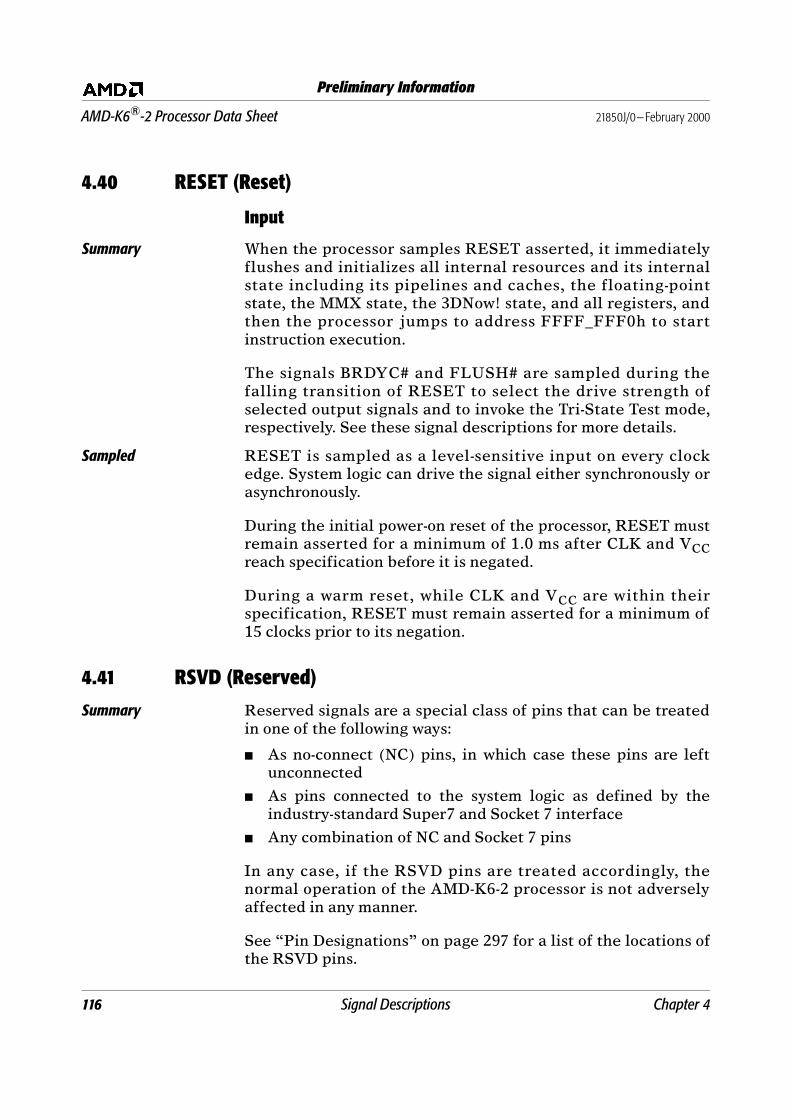
116 Signal Descriptions Chapter 4
AMD-K6®-2 Processor Data Sheet 21850J/0—February 2000
Preliminary Information
4.40 RESET (Reset)
Input
Summary When the processor samples RESET asserted, it immediately
flushes and initializes all internal resources and its internal
state including its pipelines and caches, the floating-point
state, the MMX state, the 3DNow! state, and all registers, and
then the processor jumps to address FFFF_FFF0h to start
instruction execution.
The signals BRDYC# and FLUSH# are sampled during the
falling transition of RESET to select the drive strength of
selected output signals and to invoke the Tri-State Test mode,
respectively. See these signal descriptions for more details.
Sampled RESET is sampled as a level-sensitive input on every clock
edge. System logic can drive the signal either synchronously or
asynchronously.
During the initial power-on reset of the processor, RESET must
remain asserted for a minimum of 1.0 ms after CLK and VCCreach specification before it is negated.
During a warm reset, while CLK and VCC are within their
specification, RESET must remain asserted for a minimum of
15 clocks prior to its negation.
4.41 RSVD (Reserved)
Summary Reserved signals are a special class of pins that can be treated
in one of the following ways:
As no-connect (NC) pins, in which case these pins are left
unconnected
As pins connected to the system logic as defined by the
industry-standard Super7 and Socket 7 interface
Any combination of NC and Socket 7 pins
In any case, if the RSVD pins are treated accordingly, the
normal operation of the AMD-K6-2 processor is not adversely
affected in any manner.
See “Pin Designations” on page 297 for a list of the locations of
the RSVD pins.

Chapter 4 Signal Descriptions 117
21850J/0—February 2000 AMD-K6®-2 Processor Data Sheet
Preliminary Information
4.42 SCYC (Split Cycle)
Output
Summary The processor asserts SCYC during misaligned, locked transfers
on the D[63:0] data bus. The processor generates additional bus
cycles to complete the transfer of misaligned data.
For purposes of bus cycles, the term aligned means:
Any 1-byte transfers
2-byte and 4-byte transfers that lie within 4-byte address
boundaries
8-byte transfers that lie within 8-byte address boundaries
Driven and Floated SCYC is asserted off the same clock edge as ADS#, and negated
off the clock edge on which NA# or the last expected BRDY# of
the entire locked sequence is sampled asserted. SCYC is only
valid during locked memory cycles.
SCYC is floated off the clock edge that BOFF# is sampled
asserted and off the clock edge that the processor asserts HLDA
in response to HOLD.
4.43 SMI# (System Management Interrupt)
Input, Internal Pullup
Summary The assertion of SMI# causes the processor to enter System
Management Mode (SMM). Upon recognizing SMI#, the
processor performs the following actions, in the order shown:
1. Flushes its instruction pipelines
2. Completes all pending and in-progress bus cycles
3. Acknowledges the interrupt by asserting SMIACT# after
sampling EWBE# asserted (if EWBE# is masked off, then
SMIACT# is not affected by EWBE#)
4. Saves the internal processor state in SMM memory
5. Disables interrupts by clearing the interrupt flag (IF) in
EFLAGS and disables NMI interrupts
6. Jumps to the entry point of the SMM service routine at the
SMM base physical address which defaults to 0003_8000h in
SMM memory

118 Signal Descriptions Chapter 4
AMD-K6®-2 Processor Data Sheet 21850J/0—February 2000
Preliminary Information
See “System Management Mode (SMM)” on page 211 for more
details regarding SMM.
Sampled SMI# is sampled and latched as a falling edge-sensitive signal.
SMI# is sampled on every clock edge but is not recognized until
the next instruction boundary. If SMI# is to be recognized on
the instruction boundary associated with a BRDY#, it must be
sampled asserted a minimum of three clock edges before the
BRDY# is sampled asserted. If it is asserted synchronously, it
can be asserted for a minimum of one clock. If it is asserted
asynchronously, it must have been negated for a minimum of
two clocks followed by an assertion of a minimum of two clocks.
A second assertion of SMI# while in SMM is latched but is not
recognized until the SMM service routine is exited.
4.44 SMIACT# (System Management Interrupt Active)
Output
Summary The processor acknowledges the assertion of SMI# with the
assertion of SMIACT# to indicate that the processor has
entered System Management Mode (SMM). The system logic
can use SMIACT# to enable SMM memory. See “SMI# (System
Management Interrupt)” on page 117 for more details.
See “System Management Mode (SMM)” on page 211 for more
details regarding SMM.
Driven The processor asserts SMIACT# after the last BRDY# of the last
pending bus cycle is sampled asserted (including all pending
write cycles) and after EWBE# is sampled asserted (if EWBE#
is masked off, then SMIACT# is not affected by EWBE#).
SMIACT# remains asserted until after the last BRDY# of the
last pending bus cycle associated with exiting SMM is sampled
asserted.
SMIACT# remains asserted during any flush, internal snoop, or
writeback cycle due to an inquire cycle.

Chapter 4 Signal Descriptions 119
21850J/0—February 2000 AMD-K6®-2 Processor Data Sheet
Preliminary Information
4.45 STPCLK# (Stop Clock)
Input, Internal Pullup
Summary The assertion of STPCLK# causes the processor to enter the
Stop Grant state, during which the processor’s internal clock is
stopped. From the Stop Grant state, the processor can
subsequently transition to the Stop Clock state, in which the
bus clock CLK is stopped. Upon recognizing STPCLK#, the
processor performs the following actions, in the order shown:
1. Flushes its instruction pipelines
2. Completes all pending and in-progress bus cycles
3. Acknowledges the STPCLK# assertion by executing a Stop
Grant special bus cycle (see Table 25 on page 126)
4. Stops its internal clock after BRDY# of the Stop Grant
special bus cycle is sampled asserted and after EWBE# is
sampled asserted (if EWBE# is masked off, then entry into
the Stop Grant state is not affected by EWBE#)
5. Enters the Stop Clock state if the system logic stops the bus
clock CLK (optional)
See “Clock Control” on page 243 for more details regarding
clock control.
Sampled STPCLK# is sampled as a level-sensitive input on every clock
edge but is not recognized until the next instruction boundary.
System logic can drive the signal either synchronously or
asynchronously. If it is asserted asynchronously, it must be
asserted for a minimum pulse width of two clocks.
STPCLK# must remain asserted until recognized, which is
indicated by the completion of the Stop Grant special cycle.
4.46 TCK (Test Clock)
Input, Internal Pullup
Summary TCK is the clock for boundary-scan testing using the Test
Access Port (TAP). See “Boundary-Scan Test Access Port
(TAP)” on page 223 for details regarding the operation of the
TAP controller.

120 Signal Descriptions Chapter 4
AMD-K6®-2 Processor Data Sheet 21850J/0—February 2000
Preliminary Information
Sampled The processor always samples TCK, except while TRST# is
asserted.
4.47 TDI (Test Data Input)
Input, Internal Pullup
Summary TDI is the serial test data and instruction input for
boundary-scan testing using the Test Access Port (TAP). See
“Boundary-Scan Test Access Port (TAP)” on page 223 for details
regarding the operation of the TAP controller.
Sampled The processor samples TDI on every rising TCK edge but only
while in the Shift-IR and Shift-DR states.
4.48 TDO (Test Data Output)
Output
Summary TDO is the serial test data and instruction output for
boundary-scan testing using the Test Access Port (TAP). See
“Boundary-Scan Test Access Port (TAP)” on page 223 for details
regarding the operation of the TAP controller.
Driven and Floated The processor drives TDO on every falling TCK edge but only
while in the Shift-IR and Shift-DR states. TDO is floated at all
other times.
4.49 TMS (Test Mode Select)
Input, Internal Pullup
Summary TMS specifies the test function and sequence of state changes
for boundary-scan testing using the Test Access Port (TAP). See
“Boundary-Scan Test Access Port (TAP)” on page 223 for details
regarding the operation of the TAP controller.
Sampled The processor samples TMS on every rising TCK edge. If TMS is
sampled High for five or more consecutive clocks, the TAP
controller enters its Test-Logic-Reset state, regardless of the
controller state. This action is the same as that achieved by
asserting TRST#.

Chapter 4 Signal Descriptions 121
21850J/0—February 2000 AMD-K6®-2 Processor Data Sheet
Preliminary Information
4.50 TRST# (Test Reset)
Input, Internal Pullup
Summary The assertion of TRST# initializes the Test Access Port (TAP) by
resetting its state machine to the Test-Logic-Reset state. See
“Boundary-Scan Test Access Port (TAP)” on page 223 for details
regarding the operation of the TAP controller.
Sampled TRST# is a completely asynchronous input that does not
require a minimum setup and hold time relative to TCK. See
Table 69 on page 280 for the minimum pulse width requirement.
4.51 VCC2DET (VCC2 Detect)
Output
Summary VCC2DET is internally tied to VSS (logic level 0) to indicate to
the system logic that it must supply the specified dual-voltage
requirements to the VCC2 and VCC3 pins. The VCC2 pins supply
voltage to the processor core, independent of the voltage
supplied to the I/O buffers on the VCC3 pins. Upon sampling
VCC2DET Low, system logic should sample VCC2H/L# to
identify core voltage requirements.
Driven VCC2DET always equals 0 and is never floated—even during
the Tri-State Test mode.
4.52 VCC2H/L# (VCC2 High/Low)
Output
Summary VCC2H/L# is internally tied to VSS (logic level 0) to indicate to
the system logic that it must supply the specified processor core
voltage to the VCC2 pins. The VCC2 pins supply voltage to the
processor core, independent of the voltage supplied to the I/O
buffers on the VCC3 pins. Upon sampling VCC2DET Low to
identify dual-voltage processor requirements, system logic
should sample VCC2H/L# to identify the core voltage
requirements for 2.9V and 3.2V products (High) or 2.2V and
2.4 V products (Low).
Driven VCC2H/L# always equals 0 and is never floated for 2.2V and
2.4 V products—even during the Tri-State Test mode. To ensure
proper operation for 2.9V and 3.2V products, system logic that

122 Signal Descriptions Chapter 4
AMD-K6®-2 Processor Data Sheet 21850J/0—February 2000
Preliminary Information
samples VCC2H/L# should design a weak pullup resistor for
this signal.
4.53 W/R# (Write/Read)
Output
Summary The processor drives W/R# to indicate whether it is performing
a write or a read cycle on the bus. In addition, W/R# is used to
define other bus cycles, including interrupt acknowledge and
special cycles. See Table 25 on page 126 for more details.
Driven and Floated W/R# is driven off the same clock edge as ADS# and remains in
the same state until the clock edge on which NA# or the last
expected BRDY# of the cycle is sampled asserted. W/R# is
driven during memory cycles, I/O cycles, special bus cycles, and
interrupt acknowledge cycles.
W/R# is floated off the clock edge that BOFF# is sampled
asserted and off the clock edge that the processor asserts HLDA
in response to HOLD.
Table 19. Output Pin Float Conditions
Name Floated At: Note
VCC2DET Always Driven *
VCC2H/L# Always Driven *
Note:
* All outputs except VCC2DET, VCC2H/L#, and TDO floatduring the Tri-State Test mode.

Chapter 4 Signal Descriptions 123
21850J/0—February 2000 AMD-K6®-2 Processor Data Sheet
Preliminary Information
4.54 WB/WT# (Writeback or Writethrough)
Input
Summary WB/WT#, together with PWT, specifies the data cache-line state
during cacheable read misses and write hits to shared cache
lines.
If WB/WT# = 0 or PWT = 1 during a cacheable read miss or write
hit to a shared cache line, the accessed line is cached in the
shared state. This is referred to as the writethrough state
because all write cycles to this cache line are driven externally
on the bus.
If WB/WT# = 1 and PWT = 0 during a cacheable read miss or a
write hit to a shared cache line, the accessed line is cached in
the exclusive state. Subsequent write hits to the same line
cause its state to transition from exclusive to modified. This is
referred to as the writeback state because the data cache can
contain modified cache lines that are subject to be written
back—referred to as a writeback cycle—as the result of an
inquire cycle, an internal snoop, a flush operation, or the
WBINVD instruction.
Sampled WB/WT# is sampled on the clock edge that the first BRDY# or
NA# of a bus cycle is sampled asserted. If the cycle is a burst
read, WB/WT# is ignored during the last three assertions of
BRDY#. WB/WT# is sampled during memory read and
non-writeback write cycles and is ignored during all other types
of cycles.

124 Signal Descriptions Chapter 4
AMD-K6®-2 Processor Data Sheet 21850J/0—February 2000
Preliminary Information
Table 20. Input Pin Types
Name Type Note Name Type Note
A20M# Asynchronous 1 IGNNE# Asynchronous 1
AHOLD Synchronous INIT Asynchronous 2
BF[2:0] Synchronous 4 INTR Asynchronous 1
BOFF# Synchronous INV Synchronous
BRDY# Synchronous KEN# Synchronous
BRDYC# Synchronous 7 NA# Synchronous
CLK Clock NMI Asynchronous 2
EADS# Synchronous RESET Asynchronous 5, 6
EWBE# Synchronous 8 SMI# Asynchronous 2
FLUSH# Asynchronous 2, 3 STPCLK# Asynchronous 1
HOLD Synchronous WB/WT# Synchronous
Notes:
1. These level-sensitive signals can be asserted synchronously or asynchronously. To be sampled on a specific clock edge, setup andhold times must be met. If asserted asynchronously, they must be asserted for a minimum pulse width of two clocks.
2. These edge-sensitive signals can be asserted synchronously or asynchronously. To be sampled on a specific clock edge, setup andhold times must be met. If asserted asynchronously, they must have been negated at least two clocks prior to assertion and mustremain asserted at least two clocks.
3. FLUSH# is also sampled during the falling transition of RESET and can be asserted synchronously or asynchronously. To besampled on a specific clock edge, setup and hold times must be met relative to the clock edge before the clock edge on whichRESET is sampled negated. If asserted asynchronously, FLUSH# must meet a minimum setup and hold time of two clocks relativeto the negation of RESET.
4. BF[2:0] are sampled during the falling transition of RESET. They must meet a minimum setup time of 1.0 ms and a minimum holdtime of two clocks relative to the negation of RESET.
5. During the initial power-on reset of the processor, RESET must remain asserted for a minimum of 1.0 ms after CLK and VCC reachspecification before it is negated.
6. During a warm reset, while CLK and VCC are within their specification, RESET must remain asserted for a minimum of 15 clocksprior to its negation.
7. BRDYC# is also sampled during the falling transition of RESET. If RESET is driven synchronously, BRDYC# must meet the specifiedhold time relative to the negation of RESET. If asserted asynchronously, BRDYC# must meet a minimum setup and hold time oftwo clocks relative to the negation of RESET.
8. On the AMD-K6-2 processor Model 8/[F:8], if EFER[3] is set to 1, then EWBE# is ignored by the processor.

Chapter 4 Signal Descriptions 125
21850J/0—February 2000 AMD-K6®-2 Processor Data Sheet
Preliminary Information
Table 21. Output Pin Float Conditions
Name Floated At: (Note 1) Note Name Floated At: (Note 1) Note
A[4:3] HLDA, AHOLD, BOFF# 2, 3 HLDA Always Driven
ADS# HLDA, BOFF# 2 LOCK# HLDA, BOFF# 2
ADSC# HLDA, BOFF# 2 M/IO# HLDA, BOFF# 2
APCHK# Always Driven PCD HLDA, BOFF# 2
BE[7:0]# HLDA, BOFF# 2 PCHK# Always Driven
BREQ Always Driven PWT HLDA, BOFF# 2
CACHE# HLDA, BOFF# 2 SCYC HLDA, BOFF# 2
D/C# HLDA, BOFF# 2 SMIACT# Always Driven
FERR# Always Driven VCC2DET Always Driven
HIT# Always Driven VCC2H/L# Always Driven
HITM# Always Driven W/R# HLDA, BOFF# 2
Notes:
1. All outputs except VCC2DET, VCC2H/L#, and TDO float during the Tri-State Test mode.
2. Floated off the clock edge that BOFF# is sampled asserted and off the clock edge that HLDA is asserted.
3. Floated off the clock edge that AHOLD is sampled asserted.
Table 22. Input/Output Pin Float Conditions
Name Floated At: (Note 1) Note
A[31:5] HLDA, AHOLD, BOFF# 2,3
AP HLDA, AHOLD, BOFF# 2,3
D[63:0] HLDA, BOFF# 2
DP[7:0] HLDA, BOFF# 2
Notes:
1. All outputs except VCC2DET and TDO float during the Tri-State Test mode.
2. Floated off the clock edge that BOFF# is sampled asserted and off the clock edge that HLDA is asserted.
3. Floated off the clock edge that AHOLD is sampled asserted.
Table 23. Test Pins
Name Type Note
TCK Clock
TDI Input Sampled on the rising edge of TCK
TDO Output Driven on the falling edge of TCK
TMS Input Sampled on the rising edge of TCK
TRST# Input Asynchronous (Independent of TCK)

126 Signal Descriptions Chapter 4
AMD-K6®-2 Processor Data Sheet 21850J/0—February 2000
Preliminary Information
Table 24. Bus Cycle Definition
Bus Cycle InitiatedGenerated by the Processor
Generatedby the System
M/IO# D/C# W/R# CACHE# KEN#
Code Read, Instruction Cache Line Fill 1 0 0 0 0
Code Read, Noncacheable 1 0 0 1 x
Code Read, Noncacheable 1 0 0 x 1
Encoding for Special Cycle 0 0 1 1 x
Interrupt Acknowledge 0 0 0 1 x
I/O Read 0 1 0 1 x
I/O Write 0 1 1 1 x
Memory Read, Data Cache Line Fill 1 1 0 0 0
Memory Read, Noncacheable 1 1 0 1 x
Memory Read, Noncacheable 1 1 0 x 1
Memory Write, Data Cache Writeback 1 1 1 0 x
Memory Write, Noncacheable 1 1 1 1 x
Note:
x means “don’t care”
Table 25. Special Cycles
Special Cycle
A4
BE7
#
BE6
#
BE5
#
BE4
#
BE3
#
BE2
#
BE1
#
BE0
#
M/I
O#
D/C
#
W/R
#
CA
CH
E#
KEN
#
Stop Grant 1 1 1 1 1 1 0 1 1 0 0 1 1 x
Flush Acknowledge (FLUSH# sampled asserted)
0 1 1 1 0 1 1 1 1 0 0 1 1 x
Writeback(WBINVD instruction)
0 1 1 1 1 0 1 1 1 0 0 1 1 x
Halt 0 1 1 1 1 1 0 1 1 0 0 1 1 x
Flush (INVD, WBINVD instruction)
0 1 1 1 1 1 1 0 1 0 0 1 1 x
Shutdown 0 1 1 1 1 1 1 1 0 0 0 1 1 x
Note:
x means “don’t care”

Chapter 5 Bus Cycles 127
21850J/0—February 2000 AMD-K6®-2 Processor Data Sheet
Preliminary Information
5 Bus Cycles
The following sections describe and illustrate the timing and
relationship of bus signals during various types of bus cycles. A
representative set of bus cycles is illustrated.
5.1 Timing Diagrams
The timing diagrams illustrate the signals on the external local
bus as a function of time, as measured by the bus clock (CLK).
Throughout this chapter, the term clock refers to a single
bus-clock cycle. A clock extends from one rising CLK edge to
the next rising CLK edge. The processor samples and drives
most signals relative to the rising edge of CLK. The exceptions
to this rule include the following:
BF[2:0]—Sampled on the falling edge of RESET
FLUSH#, BRDYC#—Sampled on the falling edge of RESET,
also sampled on the rising edge of CLK
All inputs and outputs are sampled relative to TCK in
Boundary-Scan Test Mode. Inputs are sampled on the rising
edge of TCK, outputs are driven off of the falling edge of
TCK.
For each signal in the timing diagrams, the High level
represents 1, the Low level represents 0, and the Middle level
represents the floating (high-impedance) state. When both the
High and Low levels are shown, the meaning depends on the
signal. A single signal indicates ‘don’t care’. In the case of bus
activity, if both High and Low levels are shown, it indicates the
processor, alternate master, or system logic is driving a value,
but this value may or may not be valid. (For example, the value
on the address bus is valid only during the assertion of ADS#,
but addresses are also driven on the bus at other times.) Figure
53 defines the different waveform representations.

128 Bus Cycles Chapter 5
AMD-K6®-2 Processor Data Sheet 21850J/0—February 2000
Preliminary Information
Figure 53. Waveform Definitions
For all active-High signals, the term asserted means the signal is
in the High-voltage state and the term negated means the signal
is in the Low-voltage state. For all active-Low signals, the term
asserted means the signal is in the Low-voltage state and the
term negated means the signal is in the High-voltage state.
Waveform
Don’t care or bus is driven
Description
Signal or bus is changing from Low to High
Signal or bus is changing from High to Low
Bus is changing
Bus is changing from valid to invalid
Signal or bus is floating
Denotes multiple clock periods

Chapter 5 Bus Cycles 129
21850J/0—February 2000 AMD-K6®-2 Processor Data Sheet
Preliminary Information
5.2 Bus State Machine Diagram
Figure 54. Bus State Machine Diagram
Last BRDY#
Last BRDY#
Bus Transition?
No
Yes
Yes
Yes
Yes
No
No
No
No
PendingRequest?
NA# SampledAsserted?
NA# SampledAsserted?
Asserted?
Asserted?
Addr
Data
Pipe-A
Pipe-D
Idle
Trans
Bus State
Branch Condition
Idle Data
PipelineAddress
Transition
Address
PipelineData
Note: The processor transitions to the IDLE state on the clock edge on which BOFF# or RESET is sampled asserted.
Data-NA#Requested
Data-NA#
Last BRDY#Yes
No
Asserted?
PendingRequest?
No
Yes
No
Yes
Yes
NA# SampledAsserted?
Yes
No

130 Bus Cycles Chapter 5
AMD-K6®-2 Processor Data Sheet 21850J/0—February 2000
Preliminary Information
Idle The processor does not drive the system bus in the Idle state
and remains in this state until a new bus cycle is requested. The
processor enters this state off the clock edge on which the last
BRDY# of a cycle is sampled asserted during the following
conditions:
The processor is in the Data state
The processor is in the Data-NA# Requested state and no
internal pending cycle is requested
In addition, the processor is forced into this state when the
system logic asserts RESET or BOFF#. The transition to this
state occurs on the clock edge on which RESET or BOFF# is
sampled asserted.
Address In this state, the processor drives ADS# to indicate the
beginning of a new bus cycle by validating the address and
control signals. The processor remains in this state for one clock
and unconditionally enters the Data state on the next clock
edge.
Data In the Data state, the processor drives the data bus during a
write cycle or expects data to be returned during a read cycle.
The processor remains in this state until either NA# or the last
BRDY# is sampled asserted. If the last BRDY# is sampled
asserted or both the last BRDY# and NA# are sampled asserted
on the same clock edge, the processor enters the Idle state. If
NA# is sampled asserted first, the processor enters the
Data-NA# Requested state.
Data-NA# Requested If the processor samples NA# asserted while in the Data state
and the current bus cycle is not completed (the last BRDY# is
not sampled asserted), it enters the Data-NA# Requested state.
The processor remains in this state until either the last BRDY#
is sampled asserted or an internal pending cycle is requested. If
the last BRDY# is sampled asserted before the processor drives
a new bus cycle, the processor enters the Idle state (no internal
pending cycle is requested) or the Address state (processor has
a internal pending cycle).
Pipeline Address In this state, the processor drives ADS# to indicate the
beginning of a new bus cycle by validating the address and
control signals. In this state, the processor is still waiting for the
current bus cycle to be completed (until the last BRDY# is

Chapter 5 Bus Cycles 131
21850J/0—February 2000 AMD-K6®-2 Processor Data Sheet
Preliminary Information
sampled asserted). If the last BRDY# is not sampled asserted,
the processor enters the Pipeline Data state.
If the processor samples the last BRDY# asserted in this state, it
determines if a bus transition is required between the current
bus cycle and the pipelined bus cycle. A bus transition is
required when the data bus direction changes between bus
cycles, such as a memory write cycle followed by a memory read
cycle. If a bus transition is required, the processor enters the
Transition state for one clock to prevent data bus contention. If
a bus transition is not required, the processor enters the Data
state.
The processor does not transition to the Data-NA# Requested
state from the Pipeline Address state because the processor
does not begin sampling NA# until it has exited the Pipeline
Address state.
Pipeline Data Two bus cycles are concurrently executing in this state. The
processor cannot issue any additional bus cycles until the
current bus cycle is completed. The processor drives the data
bus during write cycles or expects data to be returned during
read cycles for the current bus cycle until the last BRDY# of the
current bus cycle is sampled asserted.
If the processor samples the last BRDY# asserted in this state, it
determines if a bus transition is required between the current
bus cycle and the pipelined bus cycle. If the bus transition is
required, the processor enters the Transition state for one clock
to prevent data bus contention. If a bus transition is not
required, the processor enters the Data state (NA# was not
sampled asserted) or the Data-NA# Requested state (NA# was
sampled asserted).
Transition The processor enters this state for one clock during data bus
transitions and enters the Data state on the next clock edge if
NA# is not sampled asserted. The sole purpose of this state is to
avoid bus contention caused by bus transitions during pipeline
operation.

132 Bus Cycles Chapter 5
AMD-K6®-2 Processor Data Sheet 21850J/0—February 2000
Preliminary Information
5.3 Memory Reads and Writes
The AMD-K6-2 processor performs single or burst memory bus
cycles. The single-transfer memory bus cycle transfers 1, 2, 4, or
8 bytes and requires a minimum of two clocks. Misaligned
instructions or operands result in a split cycle, which requires
multiple transactions on the bus. A burst cycle consists of four
back-to-back 8-byte (64-bit) transfers on the data bus.
Single-Transfer Memory Read and Write
Figure 55 shows a single-transfer read from memory, followed by
two single-transfer writes to memory. For the memory read
cycle, the processor asserts ADS# for one clock to validate the
bus cycle and also drives A[31:3], BE[7:0]#, D/C#, W/R#, and
M/IO# to the bus. The processor then waits for the system logic
to return the data on D[63:0] (with DP[7:0] for parity checking)
and assert BRDY#. The processor samples BRDY# on every clock
edge starting with the clock edge after the clock edge that
negates ADS#. See “BRDY# (Burst Ready)” on page 94.
During the read cycle, the processor drives PCD, PWT, and
CACHE# to indicate its caching and cache-coherency intent for
the access. The system logic returns KEN# and WB/WT# to
either confirm or change this intent. If the processor asserts
PCD and negates CACHE#, the accesses are noncacheable, even
though the system logic asserts KEN# during the BRDY# to
indicate its support for cacheability. The processor (which
drives CACHE#) and the system logic (which drives KEN#) must
agree in order for an access to be cacheable.
The processor can drive another cycle (in this example, a write
cycle) by asserting ADS# off the next clock edge after BRDY# is
sampled asserted. Therefore, an idle clock is guaranteed
between any two bus cycles. The processor drives D[63:0] with
valid data one clock edge after the clock edge on which ADS# is
asserted. To minimize processor idle times, the system logic
stores the address and data in write buffers, returns BRDY#, and
performs the store to memory later. If the processor samples
EWBE# negated during a write cycle, it suspends certain
activities until EWBE# is sampled asserted. See “EWBE#
(External Write Buffer Empty)” on page 101. In Figure 55, the
second write cycle occurs during the execution of a serializing
instruction. The processor delays the following cycle until
EWBE# is sampled asserted.

Chapter 5 Bus Cycles 133
21850J/0—February 2000 AMD-K6®-2 Processor Data Sheet
Preliminary Information
Figure 55. Non-Pipelined Single-Transfer Memory Read/Write and Write Delayed by EWBE#
Read Cycle Write Cycle (Next Cycle Delayed by EWBE#)Write Cycle
CLK
A[31:3]
BE[7:0]#
ADS#
M/IO#
D/C#
W/R#
BREQ
D[63:0]
DP[7:0]
CACHE#
EWBE#
KEN#
BRDY#
WB/WT#
ADDR DATA IDLE ADDR ADDRDATA IDLEDATA DATA DATA IDLE IDLE IDLE IDLE IDLE ADDR

134 Bus Cycles Chapter 5
AMD-K6®-2 Processor Data Sheet 21850J/0—February 2000
Preliminary Information
Misaligned Single-Transfer Memory Read and Write
Figure 56 shows a misaligned (split) memory read followed by a
misaligned memory write. Any cycle that is not aligned as
defined in “SCYC (Split Cycle)” on page 117 is considered
misaligned. When the processor encounters a misaligned
access, it determines the appropriate pair of bus cycles—each
with its own ADS# and BRDY#— required to complete the
access.
The AMD-K6-2 processor performs misaligned memory reads
and memory writes using least-significant bytes (LSBs) first
followed by most-significant bytes (MSBs). Table 26 shows the
order. In the first memory read cycle in Figure 56, the processor
reads the least-significant bytes. Immediately after the
processor samples BRDY# asserted, it drives the second bus
cycle to read the most-significant bytes to complete the
misaligned transfer.
Similarly, the misaligned memory write cycle in Figure 56 on
page 135 transfers the LSBs to the memory bus first. In the next
cycle, after the processor samples BRDY# asserted, the MSBs
are written to the memory bus.
Table 26. Bus-Cycle Order During Misaligned Transfers
Type of Access First Cycle Second Cycle
Memory Read LSBs MSBs
Memory Write LSBs MSBs

Chapter 5 Bus Cycles 135
21850J/0—February 2000 AMD-K6®-2 Processor Data Sheet
Preliminary Information
Figure 56. Misaligned Single-Transfer Memory Read and Write
LSB MSB LSB MSB
Memory Read (Misaligned) Memory Write (Misaligned)
CLK
A[31:3]
BE[7:0]#
ADS#
M/IO#
D/C#
W/R#
D[63:0]
BRDY#
ADDR DATA DATA IDLE ADDR DATA DATA IDLE ADDR DATA DATA IDLEDATA ADDR DATA DATA IDLEDATA

136 Bus Cycles Chapter 5
AMD-K6®-2 Processor Data Sheet 21850J/0—February 2000
Preliminary Information
Burst Reads and Pipelined Burst Reads
Figure 57 shows normal burst read cycles and a pipelined burst
read cycle. The AMD-K6-2 processor drives CACHE# and ADS#
together to specify that the current bus cycle is a burst cycle. If
the processor samples KEN# asserted with the first BRDY#, it
performs burst transfers. During the burst transfers, the system
logic must ignore BE[7:0]# and must return all eight bytes
beginning at the starting address the processor asserts on
A[31:3]. Depending on the starting address, the system logic
must determine the successive quadword addresses (A[4:3]) for
each transfer in a burst, as shown in Table 27. The processor
expects the second, third, and fourth quadwords to occur in the
sequences shown in Table 27.
In Figure 57, the processor drives CACHE# throughout all burst
read cycles. In the first burst read cycle, the processor drives
ADS# and CACHE#, then samples BRDY# on every clock edge
starting with the clock edge after the clock edge that negates
ADS#. The processor samples KEN# asserted on the clock edge
on which the first BRDY# is sampled asserted, executes a
32-byte burst read cycle, and expects a total of four BRDY#
signals. An ideal no-wait state access is shown in Figure 57,
whereas most system logic solutions add wait states between
the transfers.
The second burst read cycle illustrates a similar sequence, but
the processor samples NA# asserted on the same clock edge
that the first BRDY# is sampled asserted. NA# assertion
indicates the system logic is requesting the processor to output
the next address early (also known as a pipeline transfer
request). Without waiting for the current cycle to complete, the
processor drives ADS# and related signals for the next burst
cycle. Pipelining can reduce processor cycle-to-cycle idle times.
Table 27. A[4:3] Address-Generation Sequence During Bursts
Address Driven By Processor on A[4:3]
A[4:3] Addresses of SubsequentQuadwords* Generated By System Logic
Quadword 1 Quadword 2 Quadword 3 Quadword 4
00b 01b 10b 11b
01b 00b 11b 10b
10b 11b 00b 01b
11b 10b 01b 00b
Note:
* quadword = 8 bytes

Chapter 5 Bus Cycles 137
21850J/0—February 2000 AMD-K6®-2 Processor Data Sheet
Preliminary Information
Figure 57. Burst Reads and Pipelined Burst Reads
-NA -ADDR
DATA1 DATA2 DATA3
Burst Read Pipelined Burst Read
ADDR1 ADDR2 ADDR3
Burst Read
CLK
A[31:3]
BE[7:0]#
ADS#
M/IO#
D/C#
W/R#
NA#
D[63:0]
CACHE#
KEN#
BRDY#
ADDR DATA IDLEDATADATADATA ADDR DATA DATADATA PIPE
DATA DATA DATA DATA IDLE

138 Bus Cycles Chapter 5
AMD-K6®-2 Processor Data Sheet 21850J/0—February 2000
Preliminary Information
Burst Writeback Figure 58 shows a burst read followed by a writeback
transaction. The AMD-K6-2 processor initiates writebacks
under the following conditions:
Replacement—If a cache-line fill is initiated for a cache line
currently filled with valid entries, the processor selects a
line for replacement based on a least-recently-used (LRU)
algorithm for the instruction cache, and a
least-recently-allocated (LRA) algorithm for the data cache.
Before a replacement is made to a L1 data cache line that is
in the modified state, the modified line is scheduled to be
written back to memory.
Internal Snoop—The processor snoops its instruction cache
during read or write misses to its data cache, and it snoops
its data cache during read misses to its instruction cache.
This snooping is performed to determine whether the same
address is stored in both caches, a situation that is taken to
imply the occurrence of self-modifying code. If a snoop hits a
data cache line in the modified state, the line is written back
to memory before being invalidated.
WBINVD Instruction—When the processor executes a
WBINVD instruction, it writes back all modified lines in the
data cache and then invalidates all lines in both caches.
Cache Flush—When the processor samples FLUSH#
asserted, it executes a flush acknowledge special cycle and
writes back all modified lines in the data cache and then
invalidates all lines in both caches.
The processor drives writeback cycles during inquire or cache
flush cycles. The writeback shown in Figure 58 is caused by a
cache-line replacement. The processor completes the burst read
cycle that fills the cache line. Immediately following the burst
read cycle is the burst writeback cycle that represents the
modified line to be written back to memory. D[63:0] are driven
one clock edge after the clock edge on which ADS# is asserted
and are subsequently changed off the clock edge on which each
of the four BRDY# signals of the burst cycle are sampled
asserted.

Chapter 5 Bus Cycles 139
21850J/0—February 2000 AMD-K6®-2 Processor Data Sheet
Preliminary Information
Figure 58. Burst Writeback due to Cache-Line Replacement
Burst Read Burst Writeback from L1 Cache
CLK
A[31:3]
BE[7:0]#
ADS#
CACHE#
M/IO#
D/C#
W/R#
D[63:0]
KEN#
BRDY#
WB/WT#
ADDR DATA IDLEDATADATA DATA ADDR DATA IDLEDATADATA DATA

140 Bus Cycles Chapter 5
AMD-K6®-2 Processor Data Sheet 21850J/0—February 2000
Preliminary Information
5.4 I/O Read and Write
Basic I/O Read and Write
The processor accesses I/O when it executes an I/O instruction
(for example, IN or OUT). Figure 59 shows an I/O read followed
by an I/O write. The processor drives M/IO# Low and D/C# High
during I/O cycles. In this example, the first cycle shows a single
wait state I/O read cycle. It follows the same sequence as a
single-transfer memory read cycle. The processor drives ADS#
to initiate the bus cycle, then it samples BRDY# on every clock
edge starting with the clock edge after the clock edge that
negates ADS#. The system logic must return BRDY# to
complete the cycle. When the processor samples BRDY#
asserted, it can assert ADS# for the next cycle off the next clock
edge. (In this example, an I/O write cycle.)
The I/O write cycle is similar to a memory write cycle, but the
processor drives M/IO# low during an I/O write cycle. The
processor asserts ADS# to initiate the bus cycle. The processor
drives D[63:0] with valid data one clock edge after the clock
edge on which ADS# is asserted. The system logic must assert
BRDY# when the data is properly stored to the I/O destination.
The processor samples BRDY# on every clock edge starting with
the clock edge after the clock edge that negates ADS#. In this
example, two wait states are inserted while the processor waits
for BRDY# to be asserted.
Figure 59. Basic I/O Read and Write
I/O Read Cycle I/O Write Cycle
CLK
A[31:3]
BE[7:0]#
ADS#
M/IO#
D/C#
W/R#
D[63:0]
BRDY#
ADDR DATA DATA IDLE ADDR DATA DATA DATA IDLE

Chapter 5 Bus Cycles 141
21850J/0—February 2000 AMD-K6®-2 Processor Data Sheet
Preliminary Information
Misaligned I/O Read and Write
Table 28 shows the misaligned I/O read and write cycle order
executed by the AMD-K6-2 processor. In Figure 60, the
least-significant bytes (LSBs) are transferred first. Immediately
after the processor samples BRDY# asserted, it drives the
second bus cycle to transfer the most-significant bytes (MSBs)
to complete the misaligned bus cycle.
Figure 60. Misaligned I/O Transfer
Table 28. Bus-Cycle Order During Misaligned I/O Transfers
Type of Access First Cycle Second Cycle
I/O Read LSBs MSBs
I/O Write LSBs MSBs
LSB MSB LSB MSB
Misaligned I/O Read Misaligned I/O Write
CLK
A[31:3]
BE[7:0]#
ADS#
M/IO#
D/C#
W/R#
D[63:0]
BRDY#
ADDR DATA DATA IDLE ADDR DATA DATA IDLE ADDR DATA DATADATA IDLE ADDR DATA DATADATA IDLE
SCYC

142 Bus Cycles Chapter 5
AMD-K6®-2 Processor Data Sheet 21850J/0—February 2000
Preliminary Information
5.5 Inquire and Bus Arbitration Cycles
The AMD-K6-2 processor provides built-in level-one data and
instruction caches. Each cache is 32 Kbytes and two-way
set-associative. The system logic or other bus master devices
can initiate an inquire cycle to maintain cache/memory
coherency. In response to the inquire cycle, the processor
compares the inquire address with its cache tag addresses in
both caches, and, if necessary, updates the MESI state of the
cache line and performs writebacks to memory.
An inquire cycle can be initiated by asserting AHOLD, BOFF#,
or HOLD. AHOLD is exclusively used to support inquire cycles.
During AHOLD-initiated inquire cycles, the processor only
floats the address bus. BOFF# provides the fastest access to the
bus because it aborts any processor cycle that is in-progress,
whereas AHOLD and HOLD both permit an in-progress bus
cycle to complete. During HOLD-initiated and BOFF#-initiated
inquire cycles, the processor floats all of its bus-driving signals.
Hold and Hold Acknowledge Cycle
The system logic or another bus device can assert HOLD to
initiate an inquire cycle or to gain full control of the bus. When
the AMD-K6-2 processor samples HOLD asserted, it completes
any in-progress bus cycle and asserts HLDA to acknowledge
release of the bus. The processor floats the following signals off
the same clock edge that HLDA is asserted:
Figure 61 shows a basic HOLD/HLDA operation. In this
example, the processor samples HOLD asserted during the
memory read cycle. It continues the current memory read cycle
until BRDY# is sampled asserted. The processor drives HLDA
and floats its outputs one clock edge after the last BRDY# of the
cycle is sampled asserted. The system logic can assert HOLD for
as long as it needs to utilize the bus. The processor samples
A[31:3] DP[7:0]
ADS# LOCK#
AP# M/IO#
BE[7:0]# PCD
CACHE# PWT
D[63:0] SCYC
D/C# W/R#

Chapter 5 Bus Cycles 143
21850J/0—February 2000 AMD-K6®-2 Processor Data Sheet
Preliminary Information
HOLD on every clock edge but does not assert HLDA until any
in-progress cycle or sequence of locked cycles is completed.
When the processor samples HOLD negated during a hold
acknowledge cycle, it negates HLDA off the next clock edge.
The processor regains control of the bus and can assert ADS#
off the same clock edge on which HLDA is negated.
Figure 61. Basic HOLD/HLDA Operation
CLK
A[31:3]
BE[7:0]#
ADS#
M/IO#
D/C#
W/R#
D[63:0]
HOLD
HLDA
BRDY#

144 Bus Cycles Chapter 5
AMD-K6®-2 Processor Data Sheet 21850J/0—February 2000
Preliminary Information
HOLD-Initiated Inquire Hit to Shared or Exclusive Line
Figure 62 shows a HOLD-initiated inquire cycle. In this
example, the processor samples HOLD asserted during the
burst memory read cycle. The processor completes the current
cycle (until the last expected BRDY# is sampled asserted),
asserts HLDA and floats its outputs as described on page 142.
The system logic drives an inquire cycle within the hold
acknowledge cycle. It asserts EADS#, which validates the
inquire address on A[31:5]. If EADS# is sampled asserted
before HOLD is sampled negated, the processor recognizes it as
a valid inquire cycle.
In Figure 62, the processor asserts HIT# and negates HITM# on
the clock edge after the clock edge on which EADS# is sampled
asserted, indicating the current inquire cycle hit a shared or
exclusive cache line. (Shared and exclusive cache lines have not
been modified and do not need to be written back.) During an
inquire cycle, the processor samples INV to determine whether
the addressed cache line found in the processor’s instruction or
data cache transitions to the invalid state or the shared state. In
this example, the processor samples INV asserted with EADS#,
which invalidates the cache line.
The system logic can negate HOLD off the same clock edge on
which EADS# is sampled asserted. The processor continues
driving HIT# in the same state until the next inquire cycle.
HITM# is not asserted unless HIT# is asserted.

Chapter 5 Bus Cycles 145
21850J/0—February 2000 AMD-K6®-2 Processor Data Sheet
Preliminary Information
Figure 62. HOLD-Initiated Inquire Hit to Shared or Exclusive Line
Burst Memory Read Inquire
CLK
A[31:3]
BE[7:0]#
ADS#
M/IO#
D/C#
W/R#
HIT#
HITM#
D[63:0]
KEN#
BRDY#
HOLD
HLDA
EADS#
INV

146 Bus Cycles Chapter 5
AMD-K6®-2 Processor Data Sheet 21850J/0—February 2000
Preliminary Information
HOLD-Initiated Inquire Hit to Modified Line
Figure 63 shows the same sequence as Figure 62, but in Figure
63 the inquire cycle hits a modified line and the processor
asserts both HIT# and HITM#. In this example, the processor
performs a writeback cycle immediately after the inquire cycle.
It updates the modified cache line to external memory
(normally, external cache or DRAM). The processor uses the
address (A[31:5]) that was latched during the inquire cycle to
perform the writeback cycle. The processor asserts HITM#
throughout the writeback cycle and negates HITM# one clock
edge after the last expected BRDY# of the writeback is sampled
asserted.
When the processor samples EADS# during the inquire cycle, it
also samples INV to determine the cache line MESI state after
the inquire cycle. If INV is sampled asserted during an inquire
cycle, the processor transitions the line (if found) to the invalid
state, regardless of its previous state. The cache line
invalidation operation is not visible on the bus. If INV is
sampled negated during an inquire cycle, the processor
transitions the line (if found) to the shared state. In Figure 63
the processor samples INV asserted during the inquire cycle.
In a HOLD-initiated inquire cycle, the system logic can negate
HOLD off the same clock edge on which EADS# is sampled
asserted. The processor drives HIT# and HITM# on the clock
edge after the clock edge on which EADS# is sampled asserted.
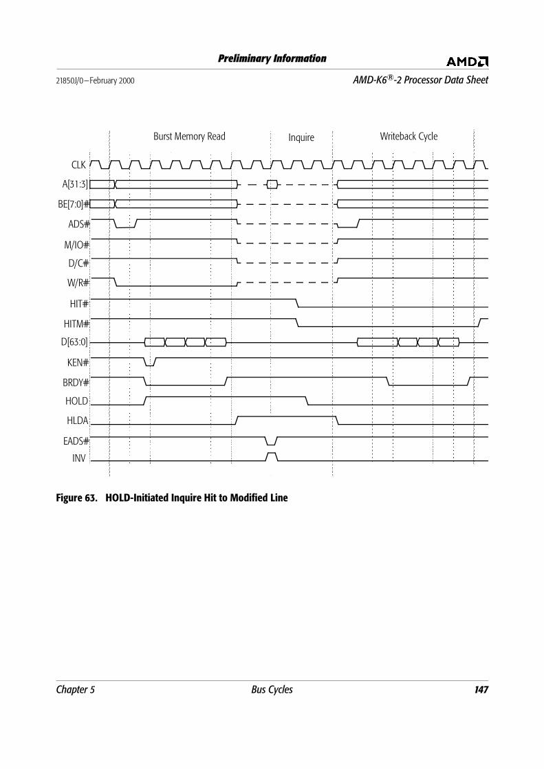
Chapter 5 Bus Cycles 147
21850J/0—February 2000 AMD-K6®-2 Processor Data Sheet
Preliminary Information
Figure 63. HOLD-Initiated Inquire Hit to Modified Line
Burst Memory Read Inquire Writeback Cycle
CLK
A[31:3]
BE[7:0]#
ADS#
M/IO#
D/C#
W/R#
EADS#
HIT#
HITM#
D[63:0]
KEN#
BRDY#
HOLD
HLDA
INV

148 Bus Cycles Chapter 5
AMD-K6®-2 Processor Data Sheet 21850J/0—February 2000
Preliminary Information
AHOLD-Initiated Inquire Miss
AHOLD can be asserted by the system to initiate one or more
inquire cycles. To allow the system to drive the address bus
during an inquire cycle, the processor floats A[31:3] and AP off
the clock edge on which AHOLD is sampled asserted. The data
bus and all other control and status signals remain under the
control of the processor and are not floated. This functionality
allows a bus cycle in progress when AHOLD is sampled asserted
to continue to completion. The processor resumes driving the
address bus off the clock edge on which AHOLD is sampled
negated.
In Figure 64, the processor samples AHOLD asserted during the
memory burst read cycle, and it floats the address bus off the
same clock edge on which it samples AHOLD asserted. While
the processor still controls the bus, it completes the current
cycle until the last expected BRDY# is sampled asserted. The
system logic drives EADS# with an inquire address on A[31:5]
during an inquire cycle. The processor samples EADS# asserted
and compares the inquire address to its tag address in both the
instruction and data caches. In Figure 64, the inquire address
misses the tag address in the processor (both HIT# and HITM#
are negated). Therefore, the processor proceeds to the next
cycle when it samples AHOLD negated. (The processor can
drive a new cycle by asserting ADS# off the same clock edge that
it samples AHOLD negated.)
For an AHOLD-initiated inquire cycle to be recognized, the
processor must sample AHOLD asserted for at least two
consecutive clocks before it samples EADS# asserted. If the
processor detects an address parity error during an inquire
cycle, APCHK# is asserted for one clock. The system logic must
respond appropriately to the assertion of this signal.
Chapter 5 Bus Cycles 149
21850J/0—February 2000 AMD-K6®-2 Processor Data Sheet
Preliminary Information
Figure 64. AHOLD-Initiated Inquire Miss
Read Inquire
CLK
A[31:3]
BE[7:0]#
AP
APCHK#
ADS#
HIT#
HITM#
D[63:0]
KEN#
BRDY#
AHOLD
EADS#
INV

150 Bus Cycles Chapter 5
AMD-K6®-2 Processor Data Sheet 21850J/0—February 2000
Preliminary Information
AHOLD-Initiated Inquire Hit to Shared or Exclusive Line
In Figure 65, the processor asserts HIT# and negates HITM# off
the clock edge after the clock edge on which EADS# is sampled
asserted, indicating the current inquire cycle hits either a
shared or exclusive line. (HIT# is driven in the same state until
the next inquire cycle.) The processor samples INV asserted
during the inquire cycle and transitions the line to the invalid
state regardless of its previous state.
During an AHOLD-initiated inquire cycle, the processor
samples AHOLD on every clock edge until it is negated. In
Figure 65, the processor asserts ADS# off the same clock on
which AHOLD is sampled negated. If the inquire cycle hits a
modified line, the processor performs a writeback cycle before
it drives a new bus cycle. The next section describes the
AHOLD-initiated inquire cycle that hits a modified line.

Chapter 5 Bus Cycles 151
21850J/0—February 2000 AMD-K6®-2 Processor Data Sheet
Preliminary Information
Figure 65. AHOLD-Initiated Inquire Hit to Shared or Exclusive Line
Burst Memory Read Inquire
CLK
A[31:3]
BE[7:0]#
ADS#
M/IO#
D/C#
W/R#
HIT#
HITM#
D[63:0]
KEN#
BRDY#
AHOLD
INV
EADS#

152 Bus Cycles Chapter 5
AMD-K6®-2 Processor Data Sheet 21850J/0—February 2000
Preliminary Information
AHOLD-Initiated Inquire Hit to Modified Line
Figure 66 shows an AHOLD-initiated inquire cycle that hits a
modified line. During the inquire cycle in this example, the
processor asserts both HIT# and HITM# on the clock edge after
the clock edge that it samples EADS# asserted. This condition
indicates that the cache line exists in the processor’s data cache
in the modified state.
If the inquire cycle hits a modified line, the processor performs
a writeback cycle immediately after the inquire cycle to update
the modified cache line to shared memory (normally external
cache or DRAM). In Figure 66, the system logic holds AHOLD
asserted throughout the inquire cycle and the processor
writeback cycle. In this case, the processor is not driving the
address bus during the writeback cycle because AHOLD is
sampled asserted. The system logic writes the data to memory
by using its latched copy of the inquire cycle address. If the
processor samples AHOLD negated before it performs the
writeback cycle, it drives the writeback cycle by using the
address (A[31:5]) that it latched during the inquire cycle.
If INV is sampled asserted during an inquire cycle, the
processor transitions the line (if found) to the invalid state,
regardless of its previous state (the cache invalidation
operation is not visible on the bus). If INV is sampled negated
during an inquire cycle, the processor transitions the line (if
found) to the shared state. In either case, if the line is found in
the modified state, the processor writes it back to memory
before changing its state. Figure 66 shows that the processor
samples INV asserted during the inquire cycle and invalidates
the cache line after the inquire cycle.

Chapter 5 Bus Cycles 153
21850J/0—February 2000 AMD-K6®-2 Processor Data Sheet
Preliminary Information
Figure 66. AHOLD-Initiated Inquire Hit to Modified Line
Burst Memory Read Inquire Writeback
CLK
A[31:3]
BE[7:0]#
ADS#
M/IO#
D/C#
W/R#
HIT#
HITM#
D[63:0]
KEN#
BRDY#
AHOLD
EADS#
INV

154 Bus Cycles Chapter 5
AMD-K6®-2 Processor Data Sheet 21850J/0—February 2000
Preliminary Information
AHOLD Restriction When the system logic drives an AHOLD-initiated inquire
cycle, it must assert AHOLD for at least two clocks before it
asserts EADS#. This requirement guarantees the processor
recognizes and responds to the inquire cycle properly. The
processor’s 32 address bus drivers turn on almost immediately
after AHOLD is sampled negated. If the processor switches the
data bus (D[63:0] and DP[7:0]) during a write cycle off the same
clock edge that switches the address bus (A[31:3] and AP), the
processor switches 102 drivers simultaneously, which can lead
to ground-bounce spikes. Therefore, before negating AHOLD
the following restrictions must be observed by the system logic:
When the system logic negates AHOLD during a write cycle,
it must ensure that AHOLD is not sampled negated on the
clock edge on which BRDY# is sampled asserted (See Figure
67).
When the system logic negates AHOLD during a writeback
cycle, it must ensure that AHOLD is not sampled negated on
the clock edge on which ADS# is negated (See Figure 67).
When a write cycle is pipelined into a read cycle, AHOLD
must not be sampled negated on the clock edge after the
clock edge on which the last BRDY# of the read cycle is
sampled asserted to avoid the processor simultaneously
driving the data bus (for the pending write cycle) and the
address bus off this same clock edge.
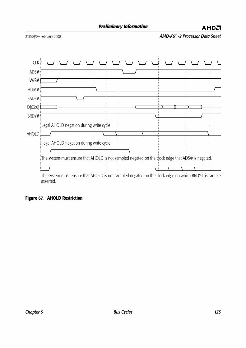
Chapter 5 Bus Cycles 155
21850J/0—February 2000 AMD-K6®-2 Processor Data Sheet
Preliminary Information
Figure 67. AHOLD Restriction
The system must ensure that AHOLD is not sampled negated on the clock edge that ADS# is negated.
Legal AHOLD negation during write cycle
Illegal AHOLD negation during write cycle
CLK
ADS#
W/R#
HITM#
EADS#
D[63:0]
BRDY#
AHOLD
The system must ensure that AHOLD is not sampled negated on the clock edge on which BRDY# is sampledasserted.

156 Bus Cycles Chapter 5
AMD-K6®-2 Processor Data Sheet 21850J/0—February 2000
Preliminary Information
Bus Backoff (BOFF#) BOFF# provides the fastest response among bus-hold inputs.
Either the system logic or another bus master can assert BOFF#
to gain control of the bus immediately. BOFF# is also used to
resolve potential deadlock problems that arise as a result of
inquire cycles. The processor samples BOFF# on every clock
edge. I f BOFF# i s sampled asserted , the processor
unconditionally aborts any cycles in progress and transitions to
a bus hold state. (See “BOFF# (Backoff)” on page 93.) Figure 68
shows a read cycle that is aborted when the processor samples
BOFF# asserted even though BRDY# is sampled asserted on the
same clock edge. The read cycle is restarted after BOFF# is
sampled negated (KEN# must be in the same state during the
restarted cycle as its state during the aborted cycle).
During a BOFF#-initiated inquire cycle that hits a shared or
exclusive line, the processor samples BOFF# negated and
restarts any bus cycle that was aborted when BOFF# was
asserted. If a BOFF#-initiated inquire cycle hits a modified line,
the processor performs a writeback cycle before it restarts the
aborted cycle.
If the processor samples BOFF# asserted on the same clock
edge that it asserts ADS#, ADS# is floated but the system logic
may erroneously interpret ADS# as asserted. In this case, the
system logic must properly interpret the state of ADS# when
BOFF# is negated.

Chapter 5 Bus Cycles 157
21850J/0—February 2000 AMD-K6®-2 Processor Data Sheet
Preliminary Information
Figure 68. BOFF# Timing
Read Back Off Cycle Restart Read Cycle
CLK
A[31:3]
BE[7:0]#
ADS#
M/IO#
D/C#
W/R#
BOFF#
D[63:0]
BRDY#

158 Bus Cycles Chapter 5
AMD-K6®-2 Processor Data Sheet 21850J/0—February 2000
Preliminary Information
Locked Cycles The processor asserts LOCK# during a sequence of bus cycles to
ensure the cycles are completed without allowing other bus
masters to intervene. Locked operations can consist of two to
five cycles. LOCK# is asserted during the following operations:
An interrupt acknowledge sequence
Descriptor Table accesses
Page Directory and Page Table accesses
XCHG instruction
An instruction with an allowable LOCK prefix
In order to ensure that locked operations appear on the bus and
are visible to the entire system, any data operands addressed
during a locked cycle that reside in the processor’s cache are
flushed and invalidated from the cache prior to the locked
operation. If the cache line is in the modified state, it is written
back and invalidated prior to the locked operation. Likewise,
any data read during a locked operation is not cached. The
processor negates LOCK# for at least one clock between
consecutive sequences of locked operations to allow the system
logic to arbitrate for the bus.
The processor asserts SCYC during misaligned locked transfers
on the D[63:0] data bus. The processor generates additional bus
cycles to complete the transfer of misaligned data.
Basic Locked Operation
Figure 69 shows a pair of read-write bus cycles. It represents a
typical read-modify-write locked operation. The processor
asserts LOCK# off the same clock edge that it asserts ADS# of
the first bus cycle in the locked operation and holds it asserted
until the last expected BRDY# of the last bus cycle in the locked
operation is sampled asserted. (The processor negates LOCK#
off the same clock edge.)

Chapter 5 Bus Cycles 159
21850J/0—February 2000 AMD-K6®-2 Processor Data Sheet
Preliminary Information
Figure 69. Basic Locked Operation
Locked Read Cycle Locked Write Cycle
CLK
A[31:3]
BE[7:0]#
ADS#
LOCK#
M/IO#
D/C#
W/R#
D[63:0]
BRDY#
ADDR DATA DATA DATA IDLE IDLE ADDR DATA DATA DATA IDLE IDLE ADDR
SCYC

160 Bus Cycles Chapter 5
AMD-K6®-2 Processor Data Sheet 21850J/0—February 2000
Preliminary Information
Locked Operation with BOFF# Intervention
Figure 70 shows BOFF# asserted within a locked read-write pair
of bus cycles. In this example, the processor asserts LOCK#
with ADS# to drive a locked memory read cycle followed by a
locked memory write cycle. During the locked memory write
cycle in this example, the processor samples BOFF# asserted.
The processor immediately aborts the locked memory write
cycle and floats all its bus-driving signals, including LOCK#.
The system logic or another bus master can initiate an inquire
cycle or drive a new bus cycle one clock edge after the clock
edge on which BOFF# is sampled asserted. If the system logic
drives a BOFF#-initiated inquire cycle and hits a modified line,
the processor performs a writeback cycle before it restarts the
locked cycle (the processor asserts LOCK# during the
writeback cycle).
In Figure 70, the processor immediately restarts the aborted
locked write cycle by driving the bus off the clock edge on
which BOFF# is sampled negated. The system logic must ensure
the processor results for interrupted and uninterrupted locked
cycles are consistent. That is, the system logic must guarantee
the memory accessed by the processor is not modified during
the time another bus master controls the bus.

Chapter 5 Bus Cycles 161
21850J/0—February 2000 AMD-K6®-2 Processor Data Sheet
Preliminary Information
Figure 70. Locked Operation with BOFF# Intervention
Locked Read Cycle Aborted Write Cycle Restart Write Cycle
CLK
A[31:3]
BE[7:0]#
ADS#
LOCK#
M/IO#
D/C#
W/R#
BOFF#
D[63:0]
BRDY#
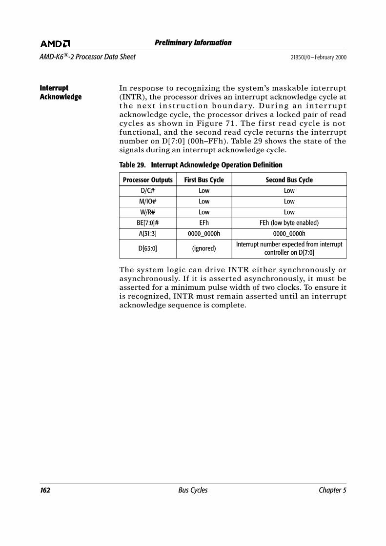
162 Bus Cycles Chapter 5
AMD-K6®-2 Processor Data Sheet 21850J/0—February 2000
Preliminary Information
Interrupt Acknowledge
In response to recognizing the system’s maskable interrupt
(INTR), the processor drives an interrupt acknowledge cycle at
the next instruct ion boundary. During an interrupt
acknowledge cycle, the processor drives a locked pair of read
cycles as shown in Figure 71. The first read cycle is not
functional, and the second read cycle returns the interrupt
number on D[7:0] (00h–FFh). Table 29 shows the state of the
signals during an interrupt acknowledge cycle.
The system logic can drive INTR either synchronously or
asynchronously. If it is asserted asynchronously, it must be
asserted for a minimum pulse width of two clocks. To ensure it
is recognized, INTR must remain asserted until an interrupt
acknowledge sequence is complete.
Table 29. Interrupt Acknowledge Operation Definition
Processor Outputs First Bus Cycle Second Bus Cycle
D/C# Low Low
M/IO# Low Low
W/R# Low Low
BE[7:0]# EFh FEh (low byte enabled)
A[31:3] 0000_0000h 0000_0000h
D[63:0] (ignored)Interrupt number expected from interrupt
controller on D[7:0]

Chapter 5 Bus Cycles 163
21850J/0—February 2000 AMD-K6®-2 Processor Data Sheet
Preliminary Information
Figure 71. Interrupt Acknowledge Operation
Interrupt Acknowledge Cycles
Interrupt Number
CLK
A[31:3]
BE[7:0]#
ADS#
M/IO#
D/C#
W/R#
LOCK#
INTR
D[63:0]
KEN#
BRDY#

164 Bus Cycles Chapter 5
AMD-K6®-2 Processor Data Sheet 21850J/0—February 2000
Preliminary Information
5.6 Special Bus Cycles
The AMD-K6-2 processor drives special bus cycles that include
stop grant, flush acknowledge, cache writeback invalidation,
halt, cache invalidation, and shutdown cycles. During all
special cycles, D/C# = 0, M/IO# = 0, and W/R# = 1. BE[7:0]# and
A[31:3] are driven to differentiate among the special cycles, as
shown in Table 30. The system logic must return BRDY# in
response to all processor special cycles.
Basic Special Bus Cycle
Figure 72 shows a basic special bus cycle. The processor drives
D/C# = 0, M/IO# = 0, and W/R# = 1 off the same clock edge that
it asserts ADS#. In this example, BE[7:0]# = FBh and A[31:3] =
0000_0000h, which indicates that the special cycle is a halt
special cycle (See Table 30). A halt special cycle is generated
after the processor executes the HLT instruction.
If the processor samples FLUSH# asserted, it writes back any
data cache lines that are in the modified state and invalidates
all lines in the instruction and data cache. The processor then
drives a flush acknowledge special cycle.
If the processor executes a WBINVD instruction, it drives a
writeback special cycle after the processor completes
invalidating and writing back the cache lines.
Table 30. Encodings For Special Bus Cycles
BE[7:0]# A[4:3]* Special Bus Cycle Cause
FBh 10b Stop Grant STPCLK# sampled asserted
EFh 00b Flush Acknowledge FLUSH# sampled asserted
F7h 00b Writeback WBINVD instruction
FBh 00b Halt HLT instruction
FDh 00b Flush INVD,WBINVD instruction
FEh 00b Shutdown Triple fault
Note:
* A[31:5] = 0

Chapter 5 Bus Cycles 165
21850J/0—February 2000 AMD-K6®-2 Processor Data Sheet
Preliminary Information
Figure 72. Basic Special Bus Cycle (Halt Cycle)
Halt Cycle
A[4:3] = 00b
FBh
CLK
A[31:3]
BE[7:0]#
ADS#
M/IO#
D/C#
W/R#
BRDY#

166 Bus Cycles Chapter 5
AMD-K6®-2 Processor Data Sheet 21850J/0—February 2000
Preliminary Information
Shutdown Cycle In Figure 73, a shutdown (triple fault) occurs in the first half of
the waveform, and a shutdown special cycle follows in the
second half. The processor enters shutdown when an interrupt
or exception occurs during the handling of a double fault (INT
8), which amounts to a triple fault. When the processor
encounters a triple fault, it stops its activity on the bus and
generates the shutdown special bus cycle (BE[7:0]# = FEh).
The system logic must assert NMI, INIT, RESET, or SMI# to get
the processor out of the shutdown state.
Figure 73. Shutdown Cycle
Shutdown Occurs(Triple Fault)
Shutdown Special Cycle
CLK
A[31:3]
BE[7:0]#
ADS#
LOCK#
M/IO#
D/C#
W/R#
D[63:0]
KEN#
BRDY#
A[4:3] = 00b
FEh

Chapter 5 Bus Cycles 167
21850J/0—February 2000 AMD-K6®-2 Processor Data Sheet
Preliminary Information
Stop Grant and Stop Clock States
Figure 74 and Figure 75 show the processor transition from
normal execution to the Stop Grant state, then to the Stop
Clock state, back to the Stop Grant state, and finally back to
normal execution. The series of transitions begins when the
processor samples STPCLK# asserted. On recognizing a
STPCLK# interrupt at the next instruction retirement
boundary, the processor performs the following actions, in the
order shown:
1. Its instruction pipelines are flushed
2. All pending and in-progress bus cycles are completed
3. The STPCLK# assertion is acknowledged by executing a
Stop Grant special bus cycle
4. Its internal clock is stopped after BRDY# of the Stop Grant
special bus cycle is sampled asserted and after EWBE# is
sampled asserted (if EWBE# is masked off, then entry into
the Stop Grant state is not affected by EWBE#)
5. The Stop Clock state is entered if the system logic stops the
bus clock CLK (optional)
STPCLK# is sampled as a level-sensitive input on every clock
edge but is not recognized until the next instruction boundary.
The system logic drives the signal either synchronously or
asynchronously. If it is asserted asynchronously, it must be
asserted for a minimum pulse width of two clocks. STPCLK#
must remain asserted until recognized, which is indicated by
the completion of the Stop Grant special cycle.

168 Bus Cycles Chapter 5
AMD-K6®-2 Processor Data Sheet 21850J/0—February 2000
Preliminary Information
Figure 74. Stop Grant and Stop Clock Modes, Part 1
STPCLK# Sampled Asserted Stop Grant Special Cycle
CLK
A[31:3]
BE[7:0]#
ADS#
M/IO#
D/C#
W/R#
CACHE#
STPCLK#
D[63:0]
KEN#
BRDY#
Stop Clock
A[4:3] = 10b
FBh
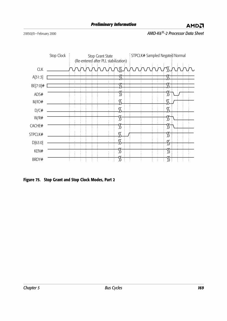
Chapter 5 Bus Cycles 169
21850J/0—February 2000 AMD-K6®-2 Processor Data Sheet
Preliminary Information
Figure 75. Stop Grant and Stop Clock Modes, Part 2
Stop Grant State(Re-entered after PLL stabilization)
STPCLK# Sampled Negated NormalStop Clock
CLK
A[31:3]
BE[7:0]#
ADS#
M/IO#
D/C#
W/R#
CACHE#
STPCLK#
D[63:0]
KEN#
BRDY#

170 Bus Cycles Chapter 5
AMD-K6®-2 Processor Data Sheet 21850J/0—February 2000
Preliminary Information
INIT-Initiated Transition from Protected Mode to Real Mode
INIT is typically asserted in response to a BIOS interrupt that
writes to an I/O port. This interrupt is often in response to a
Ctrl-Alt-Del keyboard input. The BIOS writes to a port (similar
to port 64h in the keyboard controller) that asserts INIT. INIT is
also used to support 80286 software that must return to Real
mode after accessing extended memory in Protected mode.
The assertion of INIT causes the processor to empty its
pipelines, initialize most of its internal state, and branch to
address FFFF_FFF0h—the same instruction execution starting
point used after RESET. Unlike RESET, the processor
preserves the contents of its caches, the floating-point state, the
MMX state, Model-Specific Registers (MSRs), the CD and NW
bits of the CR0 register, the time stamp counter, and other
specific internal resources.
Figure 76 shows an example in which the operating system
writes to an I/O port, causing the system logic to assert INIT.
The sampling of INIT asserted starts an extended microcode
sequence that terminates with a code fetch from FFFF_FFF0h,
the reset location. INIT is sampled on every clock edge but is
not recognized until the next instruction boundary. During an
I/O write cycle, it must be sampled asserted a minimum of three
clock edges before BRDY# is sampled asserted if it is to be
recognized on the boundary between the I/O write instruction
and the following instruction. If INIT is asserted synchronously,
it can be asserted for a minimum of one clock. If it is asserted
asynchronously, it must have been negated for a minimum of
two clocks, followed by an assertion of a minimum of two clocks.

Chapter 5 Bus Cycles 171
21850J/0—February 2000 AMD-K6®-2 Processor Data Sheet
Preliminary Information
Figure 76. INIT-Initiated Transition from Protected Mode to Real Mode
Code Fetch
FFFF_FFF0h
INIT Sampled Asserted
CLK
A[31:3]
BE[7:0]#
ADS#
M/IO#
D/C#
W/R#
D[63:0]
KEN#
BRDY#
INIT
172 Bus Cycles Chapter 5
AMD-K6®-2 Processor Data Sheet 21850J/0—February 2000
Preliminary Information

Chapter 6 Power-on Configuration and Initialization 173
21850J/0—February 2000 AMD-K6®-2 Processor Data Sheet
Preliminary Information
6 Power-on Configuration and Initialization
On power-on the system logic must reset the AMD-K6-2
processor by asserting the RESET signal. When the processor
samples RESET asserted, it immediately flushes and initializes
all internal resources and its internal state, including its
pipelines and caches, the floating-point state, the MMX and
3DNow! states, and all registers. Then the processor jumps to
address FFFF_FFF0h to start instruction execution.
6.1 Signals Sampled During the Falling Transition of RESET
FLUSH# FLUSH# is sampled on the falling transition of RESET to
determine if the processor begins normal instruction execution
or enters Tri-State Test mode. If FLUSH# is High during the
falling transition of RESET, the processor unconditionally runs
its Built-In Self Test (BIST), performs the normal reset
functions, then jumps to address FFFF_FFF0h to start
instruction execution. (See “Built-In Self-Test (BIST)” on page
221 for more details.) If FLUSH# is Low during the falling
transition of RESET, the processor enters Tri-State Test mode.
(See “Tri-State Test Mode” on page 222 and “FLUSH# (Cache
Flush)” on page 103 for more details.)
BF[2:0] The internal operating frequency of the processor is
determined by the state of the bus frequency signals BF[2:0]
when they are sampled during the falling transition of RESET.
The frequency of the CLK input signal is multiplied internally
by a ratio defined by BF[2:0]. (See “BF[2:0] (Bus Frequency)”
on page 92 for the processor-clock to bus-clock ratios.)
BRDYC# BRDYC# is sampled on the falling transition of RESET to
configure the drive strength of A[20:3], ADS#, HITM#, and
W/R#. If BRDYC# is Low during the fall of RESET, these
outputs are configured using higher drive strengths than the
standard strength. If BRDYC# is High during the fall of RESET,
the standard strength is selected. (See “BRDYC# (Burst Ready
Copy)” on page 95 for more details.)

174 Power-on Configuration and Initialization Chapter 6
AMD-K6®-2 Processor Data Sheet 21850J/0—February 2000
Preliminary Information
6.2 RESET Requirements
During the initial power-on reset of the processor, RESET must
remain asserted for a minimum of 1.0 ms after CLK and VCCreach specification. (See “CLK Switching Characteristics” on
page 267 for clock specifications. See “Electrical Data” on page
253 for VCC specifications.)
During a warm reset while CLK and VC C are within
specification, RESET must remain asserted for a minimum of
15 clocks prior to its negation.
6.3 State of Processor After RESET
Output Signals Table 31 shows the state of all processor outputs and
bidirectional signals immediately after RESET is sampled
asserted.
Registers Table 32 on page 175 shows the state of all architecture
registers and Model-Specific Registers (MSRs) after the
processor has completed its initialization due to the recognition
of the assertion of RESET.
Table 31. Output Signal State After RESET
Signal State Signal State
A[31:3], AP Floating LOCK# High
ADS#, ADSC# High M/IO# Low
APCHK# High PCD Low
BE[7:0]# Floating PCHK# High
BREQ Low PWT Low
CACHE# High SCYC Low
D/C# Low SMIACT# High
D[63:0], DP[7:0] Floating TDO Floating
FERR# High VCC2DET Low
HIT# High VCC2H/L# Low
HITM# High W/R# Low
HLDA Low – –

Chapter 6 Power-on Configuration and Initialization 175
21850J/0—February 2000 AMD-K6®-2 Processor Data Sheet
Preliminary Information
Table 32. Register State After RESET
Register State (hex) Notes
GDTR base:0000_0000h limit:0FFFFh
IDTR base:0000_0000h limit:0FFFFh
TR 0000h
LDTR 0000h
EIP FFFF_FFF0h
EFLAGS 0000_0002h
EAX 0000_0000h 1
EBX 0000_0000h
ECX 0000_0000h
EDX 0000_058Xh 2
ESI 0000_0000h
EDI 0000_0000h
EBP 0000_0000h
ESP 0000_0000h
CS F000h
SS 0000h
DS 0000h
ES 0000h
FS 0000h
GS 0000h
FPU Stack R7–R0 0000_0000_0000_0000_0000h 3
FPU Control Word 0040h 3
FPU Status Word 0000h 3
FPU Tag Word 5555h 3
FPU Instruction Pointer 0000_0000_0000h 3
FPU Data Pointer 0000_0000_0000h 3
FPU Opcode Register 000_0000_0000b 3
Notes:
1. The contents of EAX indicate if BIST was successful. If EAX = 0000_0000h, BIST was successful.If EAX is non-zero, BIST failed.
2. EDX contains the AMD-K6-2 processor signature, where X indicates the processor Stepping ID.
3. The contents of these registers are preserved following the recognition of INIT.
4. The CD and NW bits of CR0 are preserved following the recognition of INIT.
5. UWCCR, PSOR, and PFIR are implemented only on AMD-K6-2 processor Model 8/[F:8].
6. “S” represents the Stepping. “B” represents PSOR[3:0], where PSOR[3] equals 0, andPSOR[2:0] is equal to the value of the BF[2:0] signals sampled during the falling transition ofRESET.

176 Power-on Configuration and Initialization Chapter 6
AMD-K6®-2 Processor Data Sheet 21850J/0—February 2000
Preliminary Information
CR0 6000_0010h 4
CR2 0000_0000h
CR3 0000_0000h
CR4 0000_0000h
DR7 0000_0400h
DR6 FFFF_0FF0h
DR3 0000_0000h
DR2 0000_0000h
DR1 0000_0000h
DR0 0000_0000h
MCAR 0000_0000_0000_0000h 3
MCTR 0000_0000_0000_0000h 3
TR12 0000_0000_0000_0000h 3
TSC 0000_0000_0000_0000h 3
EFER0000_0000_0000_0000h (Model 8/[7:0])
0000_0000_0000_0002h (Model 8/[F:8])3
STAR 0000_0000_0000_0000h 3
WHCR 0000_0000_0000_0000h 3
UWCCR 0000_0000_0000_0000h 3, 5
PSOR 0000_0000_0000_01SBh 3, 5, 6
PFIR 0000_0000_0000_0000h 3, 5
Table 32. Register State After RESET (continued)
Register State (hex) Notes
Notes:
1. The contents of EAX indicate if BIST was successful. If EAX = 0000_0000h, BIST was successful.If EAX is non-zero, BIST failed.
2. EDX contains the AMD-K6-2 processor signature, where X indicates the processor Stepping ID.
3. The contents of these registers are preserved following the recognition of INIT.
4. The CD and NW bits of CR0 are preserved following the recognition of INIT.
5. UWCCR, PSOR, and PFIR are implemented only on AMD-K6-2 processor Model 8/[F:8].
6. “S” represents the Stepping. “B” represents PSOR[3:0], where PSOR[3] equals 0, andPSOR[2:0] is equal to the value of the BF[2:0] signals sampled during the falling transition ofRESET.

Chapter 6 Power-on Configuration and Initialization 177
21850J/0—February 2000 AMD-K6®-2 Processor Data Sheet
Preliminary Information
6.4 State of Processor After INIT
The recognition of the assertion of INIT causes the processor to
empty its pipelines, to initialize most of its internal state, and to
branch to address FFFF_FFF0h—the same instruction
execution starting point used after RESET. Unlike RESET, the
processor preserves the contents of i t s caches , the
floating-point state, the MMX and 3DNow! states, MSRs, and
the CD and NW bits of the CR0 register.
The edge-sensitive interrupts FLUSH# and SMI# are sampled
and preserved during the INIT process and are handled
accordingly after the initialization is complete. However, the
processor resets any pending NMI interrupt upon sampling
INIT asserted.
INIT can be used as an accelerator for 80286 code that requires
a reset to exit from Protected mode back to Real mode.

178 Power-on Configuration and Initialization Chapter 6
AMD-K6®-2 Processor Data Sheet 21850J/0—February 2000
Preliminary Information

Chapter 7 Cache Organization 179
21850J/0—February 2000 AMD-K6®-2 Processor Data Sheet
Preliminary Information
7 Cache Organization
The following sections describe the basic architecture and
resources of the AMD-K6-2 processor internal caches.
The performance of the AMD-K6-2 processor is enhanced by a
writeback level-one (L1) cache. The cache is organized as a
separate 32-Kbyte instruction cache and a 32-Kbyte data cache,
each with two-way set associativity (See Figure 77). The cache
line size is 32 bytes, and lines are fetched from main memory
using an efficient, pipelined burst transaction. As the
instruction cache is filled, each instruction byte is analyzed for
instruction boundaries using predecode logic. Predecoding
annotates each instruction byte with information that later
enables the decoders to efficiently decode multiple instructions
simultaneously. Translation lookaside buffers (TLB) are also
used to translate linear addresses to physical addresses. The
instruction cache is associated with a 64-entry TLB while the
data cache is associated with a 128-entry TLB.
Figure 77. Cache Organization
ProcessorCore
System Bus Interface Unit
128-Entry TLB
64-Entry TLB
State
Bit
Tag
RAMWay 0 Way 1 State
Bit
Tag
RAM
32-Kbyte Instruction Cache
32-Kbyte Data Cache
Pre-Decode Instruction Cache
MESI
Bits
Tag
RAMWay 0 Way 1 MESI
Bits
Tag
RAM

180 Cache Organization Chapter 7
AMD-K6®-2 Processor Data Sheet 21850J/0—February 2000
Preliminary Information
The processor cache design takes advantage of a sectored
organization (See Figure 78). Each sector consists of 64 bytes
configured as two 32-byte cache lines. The two cache lines of a
sector share a common tag but have separate MESI (modified,
exclusive, shared, invalid) bits that track the state of each cache
line.
Instruction Cache Line
Data Cache Line
Note: Instruction-cache lines have only two coherency states (valid or invalid) rather than
the four MESI coherency states of data-cache lines. Only two states are needed for the
instruction cache because these lines are read-only.
Figure 78. Cache Sector Organization
7.1 MESI States in the Data Cache
The state of each line in the caches is tracked by the MESI bits.
The coherency of these states or MESI bits is maintained by
internal processor snoops and external inquire cycles by the
system logic. The following four states are defined for the data
cache:
Modified—This line has been modified and is different from
main memory.
Exclusive—This line is not modified and is the same as main
memory. If this line is written to, it becomes Modified.
Shared—If a cache line is in the shared state it means that
the same line can exist in more than one cache system.
Invalid—The information in this line is not valid.
7.2 Predecode Bits
Decoding x86 instructions is particularly difficult because the
instructions vary in length, ranging from 1 to 15 bytes long.
Predecode logic supplies the predecode bits associated with
Tag
Address
Cache Line 0 Byte 31 Predecode Bits Byte 30 Predecode Bits ........ ........ Byte 0 Predecode Bits 1 MESI Bit
Cache Line 1 Byte 31 Predecode Bits Byte 30 Predecode Bits ........ ........ Byte 0 Predecode Bits 1 MESI Bit
Tag
Address
Cache Line 0 Byte 31 Byte 30 ........ ........ Byte 0 2 MESI Bits
Cache Line 1 Byte 31 Byte 30 ........ ........ Byte 0 2 MESI Bits

Chapter 7 Cache Organization 181
21850J/0—February 2000 AMD-K6®-2 Processor Data Sheet
Preliminary Information
each instruction byte. The predecode bits indicate the number
of bytes to the start of the next x86 instruction. The predecode
bits are passed with the instruction bytes to the decoders where
they assist with parallel x86 instruction decoding. The
predecode bits use memory separate from the 32-Kbyte
instruction cache. The predecode bits are stored in an extended
instruction cache alongside each x86 instruction byte as shown
in Figure 78.
7.3 Cache Operation
The operating modes for the caches are configured by software
using the not writethrough (NW) and cache disable (CD) bits of
control register 0 (CR0 bits 29 and 30, respectively). These bits
are used in all operating modes.
When the CD and NW bits are both set to 0, the cache is fully
enabled. This is the standard operating mode for the cache. If a
read miss occurs when the processor reads from the cache, a
line fill (32-byte burst read) on the system bus occurs in order to
fetch the cache line. Write hits to the cache are updated, while
write misses and writes to shared lines cause external memory
updates. Refer to Table 36 on page 193 for a summary of cache
read and write cycles and the effect of these operations on the
cache MESI state.
Note: A write allocate operation can modify the behavior of write
misses to the cache. See “Write Allocate” on page 186.
When CD is set to 0 and NW is set to 1, an invalid mode of
operation exists that causes a general protection fault to occur.
When CD is set to 1 (disabled) and NW is set to 0, the cache fill
mechanism is disabled but the contents of the cache are still
valid. The processor reads from the cache and, if a read miss
occurs, no line fill takes place. Write hits to the cache are
updated, while write misses and writes to shared lines cause
external memory updates. If PWT is driven Low and WB/WT# is
sampled High, a write hit to a shared line changes the cache-
line state to exclusive.
When the CD and NW bits are both set to 1, the cache is fully
disabled. Even though the cache is disabled, the contents are
not necessarily invalid. The processor reads from the cache and,
if a read miss occurs, no line fill takes place. If a write hit

182 Cache Organization Chapter 7
AMD-K6®-2 Processor Data Sheet 21850J/0—February 2000
Preliminary Information
occurs, the cache is updated but an external memory update
does not occur. If a data line is in the exclusive state during a
write hit, the cache-line state is changed to modified. Cache
lines in the shared state remain in the shared state after a write
hit. Write misses access external memory directly.
The operating system can control the cacheability of a page.
The paging mechanism is controlled by CR3, the Page Directory
Entry (PDE), and the Page Table Entry (PTE). Within CR3,
PDE, and PTE are Page Cache Disable (PCD) and Page
Writethrough (PWT) bits. The values of the PCD and PWT bits
used in Table 33 and Table 34 are taken from either the PTE or
PDE. For more information see the descriptions of PCD and
PWT on pages 113 and 115, respectively.
Table 33 describes how the PWT signal is driven based on the
values of the PWT bits and the PG bit of CR0.
Table 34 describes how the PCD signal is driven based on the
values of the CD bit of CR0, the PCD bits, and the PG bit of
CR0.
Table 33. PWT Signal Generation
PWT Bit* PG Bit of CR0 PWT Signal
1 1 High
0 1 Low
1 0 Low
0 0 Low
Note:
* PWT is taken from PTE or PDE
Table 34. PCD Signal Generation
CD Bit of CR0 PCD Bit* PG Bit of CR0 PCD Signal
1 X X High
0 1 1 High
0 0 1 Low
0 1 0 Low
0 0 0 Low
Note:
* PCD is taken from PTE or PDE

Chapter 7 Cache Organization 183
21850J/0—February 2000 AMD-K6®-2 Processor Data Sheet
Preliminary Information
Table 35 describes how the CACHE# signal is driven based on
the cycle type, the CI bit of TR12, the PCD signal, and the
UWCCR model-specific register.
Cache-Related Signals Complete descriptions of the signals that control cacheability
and cache coherency are given on the following pages:
CACHE#—page 96
EADS#—page 100
FLUSH#—page 103
HIT#—page 104
HITM#—page 104
INV—page 108
KEN#—page 109
PCD—page 113
PWT—page 115
WB/WT#—page 123
7.4 Cache Disabling and Flushing
To completely disable all cache accesses, the CD bit must be set
to 1 and the cache must be completely flushed.
There are three different methods for flushing the cache. The
first method relies on the system logic and other two methods
rely on software.
Table 35. CACHE# Signal Generation
Cycle Type CI Bit of TR12 PCD SignalAccess Within WC/UC Range*
CACHE#
Writebacks X X X Low
Unlocked Reads 0 0 0 Low
Locked Reads X X X High
Single Writes X X X High
Any Cycle Except Writebacks 1 X X High
Any Cycle Except Writebacks X 1 X High
Any Cycle Except Writebacks X X 1 High
Note:
* WC and UC refer to Write-Combining and Uncacheable Memory Ranges as defined in the UWCCR, and only applies to the AMD-K6-2 processor Model 8/[F:8].
184 Cache Organization Chapter 7
AMD-K6®-2 Processor Data Sheet 21850J/0—February 2000
Preliminary Information
For the system logic to flush the cache, the processor must
sample FLUSH# asserted. In this method, the processor writes
back any data cache lines that are in the modified state,
invalidates all lines in the instruction and data caches, and then
executes a flush acknowledge special cycle (See Table 25 on
page 126).
The second method for flushing the caches is for software to
execute the WBINVD instruction which causes all modified
lines to first be written back to memory, then marks all cache
lines as invalid. Alternatively, if writing modified lines back to
memory is not necessary, the INVD instruction can be used to
invalidate all cache lines.
The third and final method for flushing the caches is to make
use of the Page Flush/Invalidate Register (PFIR), which allows
cache invalidation and optional flushing of a specific 4-Kbyte
page from the linear address space. The PFIR is only supported
on the AMD-K6-2 processor Model 8/[F:8] (see “PFIR” on page
195). Unlike the previous two methods of flushing the caches,
this particular method requires the software to be aware of
which specific pages must be flushed and invalidated.
7.5 Cache-Line Fills
The processor performs a cache-line fill for any area of system
memory defined as cacheable. If an area of system memory is
not explicitly defined as uncacheable by the software or system
logic, or implicitly treated as uncacheable by the processor,
then the memory access is assumed to be cacheable.
Software can prevent caching of certain pages by setting the
PCD bit in the PDE or PTE. Additionally, for the AMD-K6-2
processor Model 8/[F:8], software can define regions of memory
as uncacheable or write combinable by programming the
MTRRs in the UWCCR MSR (see “Memory Type Range
Registers” on page 203). Write-combinable memory is defined
as uncacheable.
The system logic also has control of the cacheability of bus
cycles. If it determines the address is not cacheable, system
logic negates the KEN# signal when asserting the first BRDY#
or NA# of a cycle.

Chapter 7 Cache Organization 185
21850J/0—February 2000 AMD-K6®-2 Processor Data Sheet
Preliminary Information
The processor does not cache certain memory accesses such as
locked operations. In addition, the processor does not cache
PDE or PTE memory reads in the L1 cache (referred to as page
table walks).
When the processor needs to read memory, the processor drives
a read cycle onto the bus. If the cycle is cacheable, the
processor asserts CACHE#. If the cycle is not cacheable, a
non-burst, single-transfer read takes place. The processor waits
for the system logic to return the data and assert a single
BRDY# (See Figure 55 on page 133). If the cycle is cacheable,
the processor executes a 32-byte burst read cycle. The processor
expects a total of four BRDY# signals for a burst read cycle to
take place (See Figure 57 on page 137).
Cache-line fills initiate 32-byte burst read cycles from memory
on the system bus for the instruction cache and the data cache.
If a data-cache line being filled replaces a modified line, the
modified contents of the line are copied to a 32-byte writeback
(copyback) buffer in the bus interface unit while the new line is
being read.
7.6 Cache-Line Replacements
As programs execute and task switches occur, some cache lines
eventually require replacement.
Instruction cache lines are replaced using a Least Recently
Used (LRU) algorithm. If line replacement is required, lines are
replaced when read cache misses occur.
The data cache uses a slightly different approach to line
replacement. If a miss occurs, and a replacement is required,
lines are replaced by using a Least Recently Allocated (LRA)
algorithm.
Two forms of cache misses and associated cache fills can take
place—a tag-miss cache fill and a tag-hit cache fill. In the case
of a tag-miss cache fill, the miss is due to a tag mismatch, in
which case the required cache line is filled from external
memory, and the cache line within the sector that was not
required is marked as invalid. In the case of a tag-hit cache fill,
the address matches the tag, but the requested cache line is
marked as invalid. The required cache line is filled from
external memory, and the cache line within the sector that is
not required remains in the same cache state.

186 Cache Organization Chapter 7
AMD-K6®-2 Processor Data Sheet 21850J/0—February 2000
Preliminary Information
7.7 Write Allocate
Write allocate, if enabled, occurs when the processor has a
pending memory write cycle to a cacheable line and the line
does not currently reside in the data cache. In this case, the
processor performs a 32-byte burst read cycle to fetch the
data-cache line addressed by the pending write cycle. The data
associated with the pending write cycle is merged with the
recently-allocated data-cache line and stored in the processor’s
data cache. The final MESI state of the cache line depends on
the state of the WB/WT# and PWT signals during the burst read
cycle and the subsequent L1 data cache write hit (See Table 36
on page 193 to determine the cache-line states and the access
types following a cache read miss and cache write hit).
If a data-cache line fetch from memory is attempted because
the write allocate misses the data cache, and KEN# is sampled
negated, the processor does not perform an allocation. In this
case, the pending write cycle is executed as a single write cycle
on the system bus.
During write allocates, a 32-byte burst read cycle is executed in
place of a non-burst write cycle. While the burst read cycle
generally takes longer to execute than the non-burst write
cycle, performance gains are realized on subsequent write cycle
hits to the write-allocated cache line. Due to the nature of
software, memory accesses tend to occur in proximity of each
other (principle of locality). The likelihood of additional write
hits to the write-allocated cache line is high.
The following is a description of three mechanisms by which the
AMD-K6-2 processor performs write allocations. A write
allocate is performed when any one or more of these
mechanisms indicates that a pending write is to a cacheable
area of memory.
Write to a Cacheable Page
Every time the processor performs a cache line fill, the address
of the page in which the cache line resides is saved in the
Cacheability Control Register (CCR). The page address of
subsequent write cycles is compared with the page address
stored in the CCR. If the two addresses are equal, then the
processor performs a write allocate because the page has
already been determined to be cacheable.

Chapter 7 Cache Organization 187
21850J/0—February 2000 AMD-K6®-2 Processor Data Sheet
Preliminary Information
When the processor performs a cache line fill from a different
page than the address saved in the CCR, the CCR is updated
with the new page address.
Write to a Sector If the address of a pending write cycle matches the tag address
of a valid cache sector, but the addressed cache line within the
sector is marked invalid (a sector hit but a cache line miss),
then the processor performs a write allocate. The pending write
cycle is determined to be cacheable because the sector hit
indicates the presence of at least one valid cache line in the
sector. The two cache lines within a sector are guaranteed by
design to be within the same page.
Write Allocate Limit The AMD-K6-2 processor uses two mechanisms that are
programmable within the Write Handling Control Register
(WHCR) to enable write allocations for write cycles that
address a definable area, or a special 1-Mbyte memory area.
The format of the WHCR differs between the AMD-K6-2
processor Model 8/[7:0] and the AMD-K6-2 processor Model
8/[F:8].
WHCR – Model 8/[7:0]. This WHCR contains three fields— the
WCDE bit, the Write Allocate Enable Limit (WAELIM) field,
and the Write Allocate Enable 15-to-16-Mbyte (WAE15M) bit
(See Figure 79 on page 187).
For proper functionality, always program the WCDE bit to 0.
Figure 79. Write Handling Control Register (WHCR) — Model 8/[7:0]
Write Allocate Enable Limit – Model 8/[7:0]. The WAELIM field is 7
bits wide. This field, multiplied by 4 Mbytes, defines an upper
memory limit. Any pending write cycle that addresses memory
below this limit causes the processor to perform a write allocate
7 1 063
WAELIM
8
0
Note: Hardware RESET initializes this MSR to all zeros.
WAE15M
Symbol Description Bits WCDE Always program to 0 8
WAELIM Write Allocate Enable Limit 7–1
WAE15M Write Allocate Enable 15-to-16-Mbyte 0
9
Reserved

188 Cache Organization Chapter 7
AMD-K6®-2 Processor Data Sheet 21850J/0—February 2000
Preliminary Information
(assuming the address is not within a range where write
allocates are disallowed). Write allocate is disabled for memory
accesses at and above this limit unless the processor determines
a pending write cycle is cacheable by means of one of the other
write allocate mechanisms—“Write to a Cacheable Page” and
“Write to a Sector.” The maximum value of this memory limit is
((27 – 1) · 4 Mbytes) = 508 Mbytes. When all the bits in this field
are set to 0, all memory is above this limit and the write allocate
mechanism is disabled (even if all bits in the WAELIM field are
set to 0, write allocates can still occur due to the “Write to a
Cacheable Page” and “Write to a Sector” mechanisms).
WHCR – Model 8/[F:8]. This WHCR contains two fields—the Write
Allocate Enable Limit (WAELIM) field, and the Write Allocate
Enable 15-to-16-Mbyte (WAE15M) bit (see Figure 80).
Figure 80. Write Handling Control Register (WHCR)— Model 8/[F:8]
Write Allocate Enable Limit – Model 8/[F:8]. The WAELIM field is 10
bits wide. This field, multiplied by 4 Mbytes, defines an upper
memory limit. Any pending write cycle that addresses memory
below this limit causes the processor to perform a write allocate
(assuming the address is not within a range where write
allocates are disallowed). Write allocate is disabled for memory
accesses at and above this limit unless the processor determines
a pending write cycle is cacheable by means of one of the other
write allocate mechanisms—“Write to a Cacheable Page” and
“Write to a Sector.” The maximum value of this limit is ((210–1)
· 4 Mbytes) = 4092 Mbytes. When all the bits in this field are set
to 0, all memory is above this limit and the write allocate
mechanism is disabled (even if all bits in the WAELIM field are
1522 063
Reserved
WAELIM
16
Note: Hardware RESET initializes this MSR to all zeros.
WAE15M
Symbol Description BitsWAELIM Write Allocate Enable Limit 31-22
WAE15M Write Allocate Enable 15-to-16-Mbyte 16
17213132
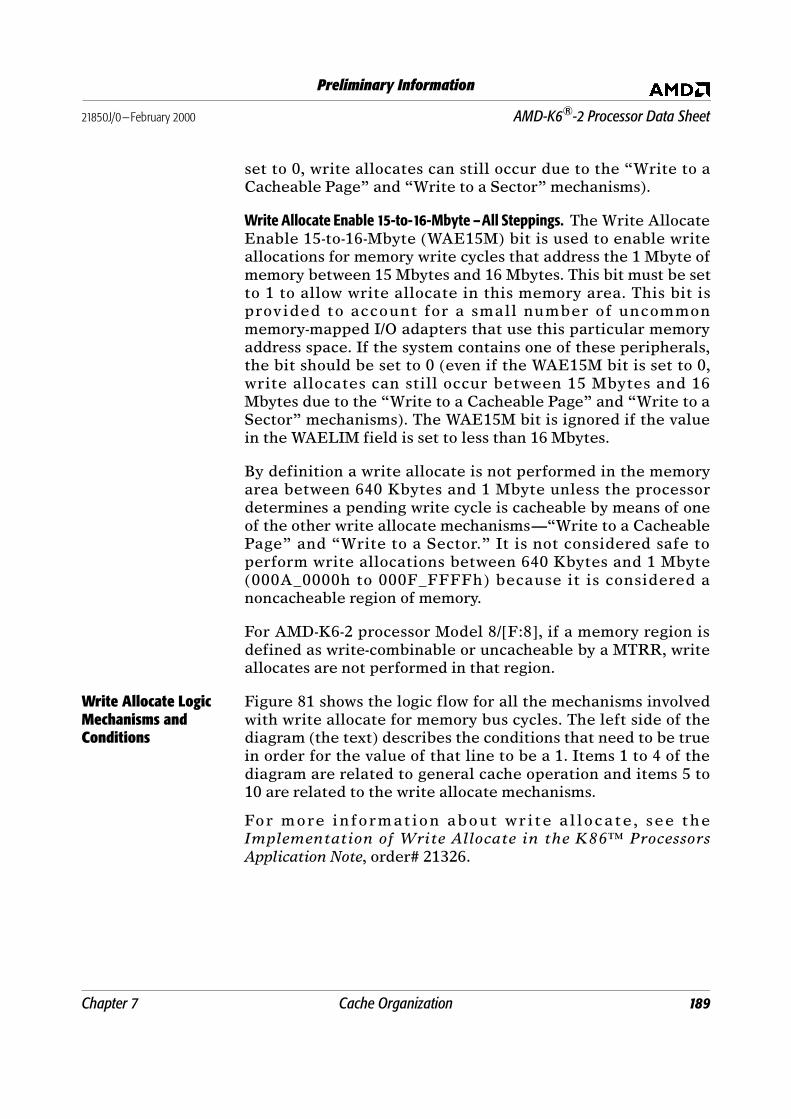
Chapter 7 Cache Organization 189
21850J/0—February 2000 AMD-K6®-2 Processor Data Sheet
Preliminary Information
set to 0, write allocates can still occur due to the “Write to a
Cacheable Page” and “Write to a Sector” mechanisms).
Write Allocate Enable 15-to-16-Mbyte –All Steppings. The Write Allocate
Enable 15-to-16-Mbyte (WAE15M) bit is used to enable write
allocations for memory write cycles that address the 1 Mbyte of
memory between 15 Mbytes and 16 Mbytes. This bit must be set
to 1 to allow write allocate in this memory area. This bit is
provided to account for a small number of uncommon
memory-mapped I/O adapters that use this particular memory
address space. If the system contains one of these peripherals,
the bit should be set to 0 (even if the WAE15M bit is set to 0,
write allocates can still occur between 15 Mbytes and 16
Mbytes due to the “Write to a Cacheable Page” and “Write to a
Sector” mechanisms). The WAE15M bit is ignored if the value
in the WAELIM field is set to less than 16 Mbytes.
By definition a write allocate is not performed in the memory
area between 640 Kbytes and 1 Mbyte unless the processor
determines a pending write cycle is cacheable by means of one
of the other write allocate mechanisms—“Write to a Cacheable
Page” and “Write to a Sector.” It is not considered safe to
perform write allocations between 640 Kbytes and 1 Mbyte
(000A_0000h to 000F_FFFFh) because it is considered a
noncacheable region of memory.
For AMD-K6-2 processor Model 8/[F:8], if a memory region is
defined as write-combinable or uncacheable by a MTRR, write
allocates are not performed in that region.
Write Allocate Logic Mechanisms and Conditions
Figure 81 shows the logic flow for all the mechanisms involved
with write allocate for memory bus cycles. The left side of the
diagram (the text) describes the conditions that need to be true
in order for the value of that line to be a 1. Items 1 to 4 of the
diagram are related to general cache operation and items 5 to
10 are related to the write allocate mechanisms.
For more informat ion about write a l locate , see the
Implementation of Write Allocate in the K86™ Processors
Application Note, order# 21326.

190 Cache Organization Chapter 7
AMD-K6®-2 Processor Data Sheet 21850J/0—February 2000
Preliminary Information
Figure 81. Write Allocate Logic Mechanisms and Conditions
The following list describes the corresponding items in Figure
81:
1. CD Bit of CR0—When the cache disable (CD) bit within
control register 0 (CR0) is set to 1, the cache fill mechanism
for both reads and writes is disabled and write allocate does
not occur.
2. PCD Signal—When the PCD (page cache disable) signal is
driven High, caching for that page is disabled, even if KEN#
is sampled asserted, and write allocate does not occur.
3. CI Bit of TR12—When the cache inhibit bit of Test Register
12 is set to 1, L1 cache fills are disabled and write allocate
does not occur.
4. UC or WC—If a pending write cycle addresses a region of
memory defined as write combinable or uncacheable by an
MTRR, write allocates are not performed in that region.
MTRRs are only supported in the AMD-K6-2 processor
Model 8/[F:8]. For all other steppings, treat this condition as
equal to 0.
5. Write to a Cacheable Page (CCR)—A write allocate is
performed if the processor knows that a page is cacheable.
The CCR is used to store the page address of the last cache
fill for a read miss. See “Write to a Cacheable Page” on page
186 for a detailed description of this condition.
1) CD Bit of CR0 Perform
Write Allocate
3) CI Bit of TR12
2) PCD Signal
5) Write to Cacheable Page (CCR)
6) Write to a Sector
8) Between 640 Kbytes and 1 Mbyte
7) Less Than Limit (WAELIM)
9) Between 15–16 Mbytes
10) Write Allocate Enable 15–16 Mbyte (WAE15M)
4) UC or WC

Chapter 7 Cache Organization 191
21850J/0—February 2000 AMD-K6®-2 Processor Data Sheet
Preliminary Information
6. Write to a Sector—A write allocate is performed if the
address of a pending write cycle matches the tag address of a
valid cache sector but the addressed cache line within the
sector is invalid. See “Write to a Sector” on page 187 for a
detailed description of this condition.
7. Less Than Limit (WAELIM)—The write allocate limit
mechanism determines if the memory area being addressed
is less than the limit set in the WAELIM field of WHCR. If
the address is less than the limit, write allocate for that
memory address is performed as long as conditions 8
through 10 do not prevent write allocate (even if conditions
8 and 10 attempt to prevent write allocate, condition 5 or 6
allows write allocate to occur).
8. Between 640 Kbytes and 1 Mbyte—Write allocate is not
performed in the memory area between 640 Kbytes and 1
Mbyte. It is not considered safe to perform write allocations
between 640 Kbytes and 1 Mbyte (000A_0000h to
000F_FFFFh) because this area of memory is considered a
noncacheable region of memory (even if condition 8
attempts to prevent write allocate, condition 5 or 6 allows
write allocate to occur).
9. Between 15–16 Mbytes—If the address of a pending write
cycle is in the 1 Mbyte of memory between 15 Mbytes and 16
Mbytes, and the WAE15M bit is set to 1, write allocate for
this cycle is enabled.
10.Write Allocate Enable 15–16 Mbytes (WAE15M)—This
condition is associated with the Write Allocate Limit
mechanism and affects write allocate only if the limit
specified by the WAELIM field is greater than or equal to
16 Mbytes. If the memory address is between 15 Mbytes and
16 Mbytes, and the WAE15M bit in the WHCR is set to 0,
write allocate for this cycle is disabled (even if condition 10
attempts to prevent write allocate, condition 5 or 6 allows
write allocate to occur).

192 Cache Organization Chapter 7
AMD-K6®-2 Processor Data Sheet 21850J/0—February 2000
Preliminary Information
7.8 Prefetching
Hardware Prefetching
The AMD-K6-2 processor conditionally performs cache
prefetching which results in the filling of the required cache
line first, and a prefetch of the second cache line making up the
other half of the sector. From the perspective of the external
bus, the two cache-line fills typically appear as two 32-byte
burst read cycles occurring back-to-back or, if allowed, as
pipelined cycles. The burst read cycles do not occur
back-to-back (wait states occur) if the processor is not ready to
start a new cycle, if higher priority data read or write requests
exist, or if NA# (next address) was sampled negated. Wait states
can also exist between burst cycles if the processor samples
AHOLD or BOFF# asserted.
Software Prefetching The 3DNow! technology includes an instruction called
PREFETCH that allows a cache line to be prefetched into the
data cache. Unlike prefetching under hardware control,
software prefetching only fetches the cache line specified by
the operand of the PREFETCH instruction, and does not
attempt to fetch the other cache line in the sector. The
PREFETCH instruction format is defined in Table 17,
“3DNow!™ Instructions,” on page 81. For more detailed
information, see the 3DNow!™ Technology Manual, order#
21928.
7.9 Cache States
Table 36 shows all the possible cache-line states before and
after program-generated accesses to individual cache lines. The
table includes the correspondence between MESI states and
writethrough or writeback states for lines in the data cache.

Chapter 7 Cache Organization 193
21850J/0—February 2000 AMD-K6®-2 Processor Data Sheet
Preliminary Information
Table 36. Data Cache States for Read and Write Accesses
TypeCache State Before
Access
Access
Type1
Cache State After Access
MESI State8 WritebackWritethrough State
Cache Read
Read Miss
invalid single read from bus invalid –
invalid burst read from bus, fill
cache2
shared or
exclusive3
writethrough or
writeback3
Read Hit
exclusive – exclusive writeback
modified – modified writeback
shared – shared writethrough
Cache Write
Write Miss
invalid single write to bus4 invalid –
invalidburst read from bus, fill
cache, write to cache5 modified6 –
invalid
burst read from bus, fill cache, write to cache,
single write to bus5shared7 –
Write Hit
exclusive or modified write to cache modified writeback
sharedwrite to cache, single
write to bus
shared or
exclusive3
writethrough or
writeback3
Notes:
1. Single read, single write, cache update, and writethrough = 1 to 8 bytes. Line fill = 32-byte burst read.
2. If CACHE# is driven Low and KEN# is sampled asserted.
3. If PWT is driven Low and WB/WT# is sampled High, the line is cached in the exclusive (writeback) state. If PWT is driven High orWB/WT# is sampled Low, the line is cached in the shared (writethrough) state.
4. Assumes the write allocate conditions as specified in “Write Allocate” on page 186 are not met.
5. Assumes the write allocate conditions as specified in “Write Allocate” on page 186 are met.
6. Assumes PWT is driven Low and WB/WT# is sampled High.
7. Assumes PWT is driven High or WB/WT# is sampled Low.
8. The final MESI state assumes that the state of the WB/WT# signal remains the same for all accesses to a particular cache line.
– Not applicable or none.

194 Cache Organization Chapter 7
AMD-K6®-2 Processor Data Sheet 21850J/0—February 2000
Preliminary Information
7.10 Cache Coherency
Different ways exist to maintain coherency between the system
memory and cache memories. Inquire cycles, internal snoops,
FLUSH#, WBINVD, INVD, and line replacements all prevent
inconsistencies between memories.
Inquire Cycles Inquire cycles are bus cycles initiated by system logic which
ensure coherency between the caches and main memory. In
systems with multiple bus masters, system logic maintains
cache coherency by driving inquire cycles to the processor.
System logic initiates inquire cycles by asserting AHOLD,
BOFF#, or HOLD to obtain control of the address bus and then
driving EADS#, INV (optional), and an inquire address
(A[31:5]). This type of bus cycle causes the processor to
compare the tags for both its instruction and data caches with
the inquire address. If there is a hit to a shared or exclusive line
in the data cache or a valid line in the instruction cache, the
processor asserts HIT#. If the compare hits a modified line in
the data cache, the processor asserts HIT# and HITM#. If
HITM# is asserted, the processor writes the modified line back
to memory. If INV was sampled asserted with EADS#, a hit
invalidates the line. If INV was sampled negated with EADS#, a
hit leaves the line in the shared state or transitions it from the
exclusive or modified state to the shared state.
Table 37 on page 197 shows the effects of inquire cycles—
performed with INV equal to 0 (non-invalidating) and INV
equal to 1 (invalidating)—snoops, and invalidations.
Internal Snooping Internal snooping is initiated by the processor (rather than
system logic) during certain cache accesses. It is used to
maintain coherency between the instruction cache and the data
cache.
The processor automatically snoops its instruction cache during
read or write misses to its data cache, and it snoops its data
cache during read misses to its instruction cache. Table 37
summarizes the actions taken during this internal snooping.

Chapter 7 Cache Organization 195
21850J/0—February 2000 AMD-K6®-2 Processor Data Sheet
Preliminary Information
If an internal snoop hits its target, the processor does the
following:
Data cache snoop during an instruction-cache read miss—If
modified, the line in the data cache is written back on the
system bus to external memory. Regardless of its state, the
data-cache line is invalidated and the instruction cache
performs a burst read cycle from external memory.
Instruction cache snoop during a data cache miss—The line in
the instruction cache is marked invalid, and the data-cache
read or write is performed as defined in Table 36 on
page 193.
FLUSH# In response to sampling FLUSH# asserted, the processor writes
back any data cache lines that are in the modified state and
then marks all lines in the instruction and data caches as
invalid.
PFIR The AMD-K6-2 processor Model 8/[F:8] processor contains the
Page Flush/Invalidate Register (PFIR) that allows cache
invalidation and optional flushing of a specific 4-Kbyte page
from the linear address space (see Figure 82). When the PFIR is
written to (using the WRMSR instruction), the invalidation
and, optionally, the flushing begins. The total amount of cache
in the AMD-K6-2 processor is 64 Kbytes. Using this register can
result in a much lower cycle count for flushing particular pages
versus flushing the entire cache.
Figure 82. Page Flush/Invalidate Register (PFIR)—MSR C000_0088h
LINPAGE. This 20-bit field must be written with bits 31:12 of the
linear address of the 4-Kbyte page that is to be invalidated and
optionally flushed from the L1 cache.
LINPAGE
1 063
F/I
Reserved
Symbol Description Bit
LINPAGE 20-bit Linear Page Address 31-12
PF Page Fault Occurred 8F/I Flush/Invalidate Command 0
1131 1232
PF
9 8 7

196 Cache Organization Chapter 7
AMD-K6®-2 Processor Data Sheet 21850J/0—February 2000
Preliminary Information
PF. If an attempt to invalidate or flush a page results in a page
fault, the processor sets the PF bit to 1, and the invalidate or
flush operation is not performed (even though invalidate
operations do not normally generate page faults). In this case,
an actual page fault exception is not generated. If the PF bit
equals 0 after an invalidate or flush operation, then the
operation executed successfully. The PF bit must be read after
every write to the PFIR register to determine if the invalidate
or flush operation executed successfully.
F/I. This bit is used to control the type of action that occurs to
the specified linear page. If a 0 is written to this bit, the
operation is a flush, in which case all cache lines in the
modified state within the specified page are written back to
memory, after which the entire page is invalidated. If a 1 is
written to this bit, the operation is an invalidation, in which
case the entire page is invalidated without the occurrence of
any writebacks.
WBINVD and INVD These x86 instructions cause all cache lines to be marked as
invalid. WBINVD writes back modified lines before marking all
cache lines invalid. INVD does not write back modified lines.
Cache-Line Replacement
Replacing lines in the instruction or data cache, according to
the line replacement algorithms described in “Cache-Line
Fills” on page 184, ensures coherency between main memory
and the caches.
Table 37 on page 197 shows all possible cache-line states before
and after various cache-related operations.

Chapter 7 Cache Organization 197
21850J/0—February 2000 AMD-K6®-2 Processor Data Sheet
Preliminary Information
Table 37. Cache States for Inquire Cycles, Snoops, Flushes, and Invalidation
Type of OperationCache State
Before OperationMemory Access
Cache State After Operation
MESI StateWriteback
Writethrough State
Inquire Cycle
shared or exclusive
–INV=0 shared writethrough
INV=1 invalid invalid
modified writeback to busINV=0 shared writethrough
INV=1 invalid invalid
Internal Snoop
shared or exclusive
–invalid invalid
modified writeback to bus
FLUSH# Signal
shared or exclusive
–invalid invalid
modified writeback to bus
PFIR* (F/I = 0)
shared or exclusive
–invalid invalid
modified writeback to bus
PFIR* (F/I = 1)
– – invalid invalid
WBINVD Instruction
shared or exclusive
–invalid invalid
modified writeback to bus
INVD Instruction
– – invalid invalid
Notes:
All writebacks are 32-byte burst write cycles.
– Not applicable or none.
* The AMD-K6-2 processor Model 8/[F:8] supports the PFIR.

198 Cache Organization Chapter 7
AMD-K6®-2 Processor Data Sheet 21850J/0—February 2000
Preliminary Information
Cache Snooping Table 38 shows the conditions under which snooping occurs in
the AMD-K6-2 processor and the resources that are snooped.
Table 38. Snoop Action
Type of Event Type of Access
Snooping Action
Instruction Cache
Data Cache
Inquire Cycle System Logic yes1 yes1
Internal Snoop
InstructionCache
ReadMiss
– yes2
ReadHit
– no
Data Cache
ReadMiss yes3 –
ReadHit
no –
WriteMiss yes3 –
WriteHit
no –
Notes:
1. The processor’s response to an inquire cycle depends on the state of the INV input signaland the state of the cache line as follows:
For the instruction cache, if INV is sampled negated, the line remains invalid or valid, butif INV is sampled asserted, the line is invalidated.
For the data cache, if INV is sampled negated, valid lines remain in or transition to theshared state, a modified data cache line is written back before the line is marked shared(with HITM# asserted), and invalid lines remain invalid. For the data cache, if INV issampled asserted, the line is marked invalid. Modified lines are written back beforeinvalidation.
2. If an internal snoop hits a modified line in the data cache, the line is written back andinvalidated. Then the instruction cache performs a burst read from memory.
3. If an internal snoop hits a line in the instruction cache, the instruction cache line isinvalidated and the data-cache read or write is performed from memory.
– Not applicable.

Chapter 7 Cache Organization 199
21850J/0—February 2000 AMD-K6®-2 Processor Data Sheet
Preliminary Information
7.11 Writethrough versus Writeback Coherency States
The terms writethrough and writeback apply to two related
concepts in a read-write cache like the AMD-K6-2 processor L1
data cache. The following conditions apply to both the
writethrough and writeback modes:
Memory Writes—A relationship exists between external
memory writes and their concurrence with cache updates:
• An external memory write that occurs concurrently with
a cache update to the same location is a writethrough.
Writethroughs are driven as single cycles on the bus.
• An external memory write that occurs after the processor
has modified a cache line is a writeback. Writebacks are
driven as burst cycles on the bus.
Coherency State—A relationship exists between MESI
coherency states and writethrough-writeback coherency
states of lines in the cache as follows:
• Shared and invalid MESI lines are in the writethrough
state.
• Modified and exclusive MESI lines are in the writeback
state.
7.12 A20M# Masking of Cache Accesses
Although the processor samples A20M# as a level-sensitive
input on every clock edge, it should only be asserted in Real
mode. The processor applies the A20M# masking to its tags,
through which all programs access the caches. Therefore,
assertion of A20M# affects all addresses (cache and external
memory), including the following:
Cache-line fills (caused by read misses or write allocates)
Cache writethroughs (caused by write misses or write hits to
lines in the shared state)
However, A20M# does not mask writebacks or invalidations
caused by the following actions:
Internal snoops
Inquire cycles
The FLUSH# signal
Writing to the PFIR (AMD-K6-2/[F:8] only)
The WBINVD instruction

200 Cache Organization Chapter 7
AMD-K6®-2 Processor Data Sheet 21850J/0—February 2000
Preliminary Information

Chapter 8 Write Merge Buffer 201
21850J/0—February 2000 AMD-K6®-2 Processor Data Sheet
Preliminary Information
8 Write Merge Buffer
The AMD-K6-2 processor Model 8/[F:8] contains an 8-byte write
merge buffer that allows the processor to conditionally combine
data from multiple noncacheable write cycles into this merge
buffer. The merge buffer operates in conjunction with the
Memory Type Range Registers (MTRRs). Refer to “Memory
Type Range Registers” on page 203 for a description of the
MTRRs.
Merging multiple write cycles into a single write cycle reduces
processor bus utilization and processor stalls, thereby
increasing the overall system performance.
8.1 EWBE Control
The presence of the merge buffer creates the potential to
perform out-of-order write cycles relative to the processor’s L1
cache. In general, the ordering of write cycles that are driven
externally on the system bus and those that hit the processor’s
cache can be controlled by the EWBE# signal. See “EWBE#
(External Write Buffer Empty)” on page 101 for more
information. If EWBE# is sampled negated, the processor
delays the commitment of write cycles to cache lines in the
modified state or exclusive state in the processor’s cache.
Therefore, the system logic can enforce strong ordering by
negating EWBE# until the external write cycle is complete,
thereby ensuring that a subsequent write cycle that hits the
cache does not complete ahead of the external write cycle.
However, the addition of the write merge buffer introduces the
potential for out-of-order write cycles to occur between writes
to the merge buffer and writes to the processor’s cache. Because
these writes occur entirely within the processor and are not
sent out to the processor bus, the system logic is not able to
enforce strong ordering with the EWBE# signal.
The EWBE control (EWBEC) bits in the EFER register provide
a mechanism for enforcing three different levels of write
ordering in the presence of the write merge buffer:
EFER[3] is defined as the Global EWBE Disable (GEWBED).
When GEWBED equals 1, the processor does not attempt to
enforce any write ordering internally or externally (the
EWBE# signal is ignored). This is the maximum performance
setting.
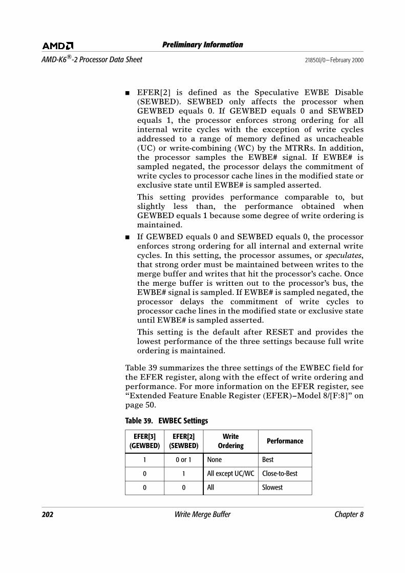
202 Write Merge Buffer Chapter 8
AMD-K6®-2 Processor Data Sheet 21850J/0—February 2000
Preliminary Information
EFER[2] is defined as the Speculative EWBE Disable
(SEWBED). SEWBED only affects the processor when
GEWBED equals 0. If GEWBED equals 0 and SEWBED
equals 1, the processor enforces strong ordering for all
internal write cycles with the exception of write cycles
addressed to a range of memory defined as uncacheable
(UC) or write-combining (WC) by the MTRRs. In addition,
the processor samples the EWBE# signal. If EWBE# is
sampled negated, the processor delays the commitment of
write cycles to processor cache lines in the modified state or
exclusive state until EWBE# is sampled asserted.
This setting provides performance comparable to, but
slightly less than, the performance obtained when
GEWBED equals 1 because some degree of write ordering is
maintained.
If GEWBED equals 0 and SEWBED equals 0, the processor
enforces strong ordering for all internal and external write
cycles. In this setting, the processor assumes, or speculates,
that strong order must be maintained between writes to the
merge buffer and writes that hit the processor’s cache. Once
the merge buffer is written out to the processor’s bus, the
EWBE# signal is sampled. If EWBE# is sampled negated, the
processor delays the commitment of write cycles to
processor cache lines in the modified state or exclusive state
until EWBE# is sampled asserted.
This setting is the default after RESET and provides the
lowest performance of the three settings because full write
ordering is maintained.
Table 39 summarizes the three settings of the EWBEC field for
the EFER register, along with the effect of write ordering and
performance. For more information on the EFER register, see
“Extended Feature Enable Register (EFER)–Model 8/[F:8]” on
page 50.
Table 39. EWBEC Settings
EFER[3]
(GEWBED)
EFER[2]
(SEWBED)
Write
OrderingPerformance
1 0 or 1 None Best
0 1 All except UC/WC Close-to-Best
0 0 All Slowest

Chapter 8 Write Merge Buffer 203
21850J/0—February 2000 AMD-K6®-2 Processor Data Sheet
Preliminary Information
8.2 Memory Type Range Registers
The AMD-K6-2 processor Model 8/[F:8] provides two variable-
range Memory Type Range Registers (MTRRs)—MTRR0 and
MTRR1—that each specify a range of memory. Each range can
be defined as one of the following memory types:
Uncacheable (UC) memory—Memory read cycles are
sourced directly from the specified memory address and the
processor does not allocate a cache line. Memory write
cycles are targeted at the specified memory address and a
write allocation does not occur.
Write-Combining (WC) memory—Memory read cycles are
sourced directly from the specified memory address and the
processor does not allocate a cache line. The processor
conditionally combines data from multiple noncacheable
write cycles that are addressed within this range into a
merge buffer. Merging multiple write cycles into a single
write cycle reduces processor bus utilization and processor
stalls, thereby increasing the overall system performance.
This memory type is applicable for linear video frame
buffers.
UC/WC Cacheability Control Register(UWCCR)
The MTRRs are accessed by addressing the 64-bit MSR known
as the UC/WC Cacheability Control Register (UWCCR). The
MSR address of the UWCCR is C000_0085h. Following reset, all
bits in the UWCCR register are set to 0. MTRR0 (lower 32 bits
of the UWCCR register) defines the size and memory type of
range 0 and MTRR1 (upper 32 bits) defines the size and
memory type of range 1 (see Figure 83).

204 Write Merge Buffer Chapter 8
AMD-K6®-2 Processor Data Sheet 21850J/0—February 2000
Preliminary Information
.
Figure 83. UC/WC Cacheability Control Register (UWCCR)—MSR C000_0085h (Model 8/[F:8])
Physical Base Address n (n=0, 1). This address is the 15 most -
significant bits of the physical base address of the memory
range. The least-significant 17 bits of the base address are not
needed because the base address is by definition always aligned
on a 128-Kbyte boundary.
Physical Address Mask n (n=0, 1). This value i s the 15 most -
significant bits of a physical address mask that is used to define
the size of the memory range. This mask is logically ANDed
with both the physical base address field of the UWCCR
register and the physical address generated by the processor. If
the results of the two AND operations are equal, then the
generated physical address is considered within the range. That
is, if:
Mask & Physical Base Address = Mask & Physical Address Generated
then the physical address generated by the processor is in the
range.
WCn (n=0, 1). When set to 1, this memory range is defined as
write combinable (refer to Table 40). Write-combinable
memory is uncacheable.
UCn (n=0, 1). When set to 1, this memory range is defined as
uncacheable (refer to Table 40).
16 063
Physical Address Mask 0
1731
Physical Base Address 0
12
Physical Address Mask 1Physical Base Address 1
3233344849
UC
0
WC
0
UC
1
WC
1
MTRR1 MTRR0
Symbol Description Bits
UC0 Uncacheable Memory Type 0
WC0 Write-Combining Memory Type 1
Symbol Description Bits
UC1 Uncacheable Memory Type 32
WC1 Write-Combining Memory Type 33

Chapter 8 Write Merge Buffer 205
21850J/0—February 2000 AMD-K6®-2 Processor Data Sheet
Preliminary Information
Memory-Range Restrictions. The following rules regarding the
address alignment and size of each range must be adhered to
when programming the physical base address and physical
address mask fields of the UWCCR register:
The minimum size of each range is 128 Kbytes.
The physical base address must be aligned on a 128-Kbyte
boundary.
The physical base address must be range-size aligned. For
example, if the size of the range is 1 Mbyte, then the
physical base address must be aligned on a 1-Mbyte
boundary.
All bits set to 1 in the physical address mask must be
contiguous. Likewise, all bits set to 0 in the physical address
mask must be contiguous. For example:
111_1111_1100_0000b is a valid physical address mask
111_1111_1101_0000b is invalid
Table 41 lists the valid physical address masks and the resulting
range sizes that can be programmed in the UWCCR register.
Table 40. WC/UC Memory Type
WCn UCn Memory Type
0 0 No effect on cacheability or write combining
1 0 Write-combining memory range (uncacheable)
0 or 1 1 Uncacheable memory range
Table 41. Valid Masks and Range Sizes
Masks Size
111_1111_1111_1111b 128 Kbytes
111_1111_1111_1110b 256 Kbytes
111_1111_1111_1100b 512 Kbytes
111_1111_1111_1000b 1 Mbyte
111_1111_1111_0000b 2 Mbytes
111_1111_1110_0000b 4 Mbytes
111_1111_1100_0000b 8 Mbytes

206 Write Merge Buffer Chapter 8
AMD-K6®-2 Processor Data Sheet 21850J/0—February 2000
Preliminary Information
Example. Suppose that the range of memory from 16 Mbytes to
32 Mbytes is uncacheable, and the 8-Mbyte range of memory on
top of 1 Gbyte is write-combinable. Range 0 is defined as the
uncacheable range, and range 1 is defined as the write-
combining range.
Extracting the 15 most-significant bits of the 32-bit physical
base address that corresponds to 16 Mbytes (0100_0000h) yields
a physical base address 0 field of 000_0000_1000_0000b.
Because the uncacheable range size is 16 Mbytes, the physical
mask value 0 field is 111_1111_1000_0000b, according to Table
41. Bit 1 of the UWCCR register (WC0) is set to 0 and bit 0 of
the UWCCR register is set to 1 (UC0).
Extracting the 15 most-significant bits of the 32-bit physical
base address that corresponds to 1 Gbyte (4000_0000h) yields a
physical base address 1 field of 010_0000_0000_0000b. Because
the write-combining range size is 8 Mbytes, the physical mask
value 1 field is 111_1111_1100_0000b, according to Table 41. Bit
33 of the UWCCR register (WC1) is set to 1 and bit 32 of the
UWCCR register is set to 0 (UC1).
111_1111_1000_0000b 16 Mbytes
111_1111_0000_0000b 32 Mbytes
111_1110_0000_0000b 64 Mbytes
111_1100_0000_0000b 128 Mbytes
111_1000_0000_0000b 256 Mbytes
111_0000_0000_0000b 512 Mbytes
110_0000_0000_0000b 1 Gbyte
100_0000_0000_0000b 2 Gbytes
000_0000_0000_0000b 4 Gbytes
Table 41. Valid Masks and Range Sizes (continued)
Masks Size

Chapter 9 Floating-Point and Multimedia Execution Units 207
21850J/0—February 2000 AMD-K6®-2 Processor Data Sheet
Preliminary Information
9 Floating-Point and Multimedia Execution Units
9.1 Floating-Point Execution Unit
The AMD-K6-2 processor contains an IEEE 754-compatible and
854-compatible floating-point execution unit designed to
accelerate the performance of software that utilizes the x86
floating-point instruction set. Floating-point software is
typically written to manipulate numbers that are very large or
very small, that require a high degree of precision, or that result
from complex mathematical operat ions such as
transcendentals. Applications that take advantage of
floating-point operations include geometric calculations for
graphics acceleration, scientific, statistical, and engineering
applications, and business applications that use large amounts
of high-precision data.
The high-performance floating-point execution unit contains an
adder unit, a multiplier unit, and a divide/square root unit.
These low-latency units can execute floating-point instructions
in as few as two processor clocks. To increase performance, the
processor is designed to simultaneously decode most
floating-point instructions with most short-decodeable
instructions.
See “Software Environment” on page 21 for a description of the
floating-point data types, registers, and instructions.
Handling Floating-Point Exceptions
The AMD-K6-2 processor provides the following two types of
exception handling for floating-point exceptions:
If the numeric error (NE) bit in CR0 is set to 1, the processor
invokes the interrupt 10h handler. In this manner, the
floating-point exception is completely handled by software.
If the NE bit in CR0 is set to 0, the processor requires
external logic to generate an interrupt on the INTR signal in
order to handle the exception.
External Logic Support of Floating-Point Exceptions
The processor provides the FERR# (Floating-Point Error) and
IGNNE# (Ignore Numeric Error) signals to allow the external
logic to generate the interrupt in a manner consistent with
IBM-compatible PC/AT systems. The assertion of FERR#
indicates the occurrence of an unmasked floating-point
exception resulting from the execution of a floating-point

208 Floating-Point and Multimedia Execution Units Chapter 9
AMD-K6®-2 Processor Data Sheet 21850J/0—February 2000
Preliminary Information
instruction. IGNNE# is used by the external hardware to control
the effect of an unmasked floating-point exception. Under
certain circumstances, if IGNNE# is sampled asserted, the
processor ignores the floating-point exception.
Figure 84 illustrates an implementation of external logic for
supporting floating-point exceptions. The following example
explains the operation of the external logic in Figure 84:
As the result of a floating-point exception, the processor
asserts FERR#. The assertion of FERR# and the
sampling of IGNNE# negated indicates the processor has
stopped instruction execution and is waiting for an
interrupt. The assertion of FERR# leads to the assertion
of INTR by the interrupt controller. The processor
acknowledges the interrupt and jumps to the
corresponding interrupt service routine in which an I/O
write cycle to address port F0h leads to the assertion of
IGNNE#. When IGNNE# is sampled asserted, the
processor ignores the floating-point exception and
continues instruction execution. When the processor
negates FERR#, the external logic negates IGNNE#.
See “FERR# (Floating-Point Error)” on page 102 and “IGNNE#
(Ignore Numeric Exception)” on page 106 for more details.
Figure 84. External Logic for Supporting Floating-Point Exceptions
FERR# Flip-Flop
CLOCK Q
DATA Q
CLEAR
IRQ13
Interrupt Controller
I/O AddressPort F0hAMD-K6®
-2
Processor
FERR#
INTR
IGNNE#
RESET
“1”
IGNNE# Flip-Flop
CLOCK Q
DATA Q
CLEAR

Chapter 9 Floating-Point and Multimedia Execution Units 209
21850J/0—February 2000 AMD-K6®-2 Processor Data Sheet
Preliminary Information
9.2 Multimedia and 3DNow!™ Execution Units
The multimedia and 3DNow! execution units of the AMD-K6-2
processor are designed to accelerate the performance of
software written using the industry-standard MMX instructions
and the new 3DNow! instructions. Applications that can take
advantage of the MMX and 3DNow! instructions include
graphics, video and audio compression and decompression,
speech recognition, and telephony applications.
The multimedia execution unit can execute MMX instructions
in a single processor clock. All MMX and 3DNow! arithmetic
instructions are pipelined for higher performance. To increase
performance, the processor is designed to simultaneously
decode all MMX and 3DNow! instructions with most other
instructions.
For more information on MMX instructions, see the AMD-K6®
Processor Multimedia Technology Manual, order# 20726. For
more information on 3DNow! instructions, see the 3DNow!™
Technology Manual, order# 21928.
9.3 Floating-Point and MMX™/3DNow!™ Instruction Compatibility
Registers The eight 64-bit MMX registers (which are also utilized by
3DNow! instructions) are mapped on the floating-point stack.
This enables backward compatibility with all existing software.
For example, the register saving event that is performed by
operating systems during task switching requires no changes to
the operating system. The same support provided in an
operating system’s interrupt 7 handler (Device Not Available)
for saving and restoring the floating-point registers also
supports saving and restoring the MMX registers.
Exceptions There are no new exceptions defined for supporting the MMX
and 3DNow! instructions. All exceptions that occur while
decoding or executing an MMX or 3DNow! instruction are
handled in existing exception handlers without modification.
FERR# and IGNNE# MMX instructions and 3DNow! instructions do not generate
float ing-point exceptions . However, i f an unmasked
floating-point exception is pending, the processor asserts
FERR# at the instruction boundary of the next floating-point

210 Floating-Point and Multimedia Execution Units Chapter 9
AMD-K6®-2 Processor Data Sheet 21850J/0—February 2000
Preliminary Information
instruction, MMX instruction, 3DNow! instruction or WAIT
instruction.
The sampling of IGNNE# asserted only affects processor
operation during the execution of an error-sensitive
floating-point instruction, MMX instruction, 3DNow!
instruction or WAIT instruction when the NE bit in CR0 is set to
0.

Chapter 10 System Management Mode (SMM) 211
21850J/0—February 2000 AMD-K6®-2 Processor Data Sheet
Preliminary Information
10 System Management Mode (SMM)
10.1 Overview
SMM is an alternate operating mode entered by way of a system
management interrupt (SMI#) and handled by an interrupt
service routine. SMM is designed for system control activities
such as power management. These activit ies appear
transparent to conventional operating systems like DOS and
Windows. SMM is primarily targeted for use by the Basic Input
Output System (BIOS) and specialized low-level device drivers.
The code and data for SMM are stored in the SMM memory
area, which is isolated from main memory.
The processor enters SMM by the assertion of the SMI#
interrupt and the processor’s acknowledgment by the assertion
of SMIACT#. At this point the processor saves its state into the
SMM memory state-save area and jumps to the SMM service
routine. The processor returns from SMM when it executes the
RSM (resume) instruction from within the SMM service
routine. Subsequently, the processor restores its state from the
SMM save area, negates SMIACT#, and resumes execution with
the instruction following the point where it entered SMM.
The following sections summarize the SMM state-save area,
entry into and exit from SMM, exceptions and interrupts in
SMM, memory allocation and addressing in SMM, and the SMI#
and SMIACT# signals.
10.2 SMM Operating Mode and Default Register Values
The software environment within SMM has the following
characteristics:
Addressing and operation in Real mode
4-Gbyte segment limits
Default 16-bit operand, address, and stack sizes, although
instruction prefixes can override these defaults
Control transfers that do not override the default operand
size truncate the EIP to 16 bits

212 System Management Mode (SMM) Chapter 10
AMD-K6®-2 Processor Data Sheet 21850J/0—February 2000
Preliminary Information
Far jumps or calls cannot transfer control to a segment with
a base address requiring more than 20 bits, as in Real mode
segment-base addressing
A20M# is masked
Interrupt vectors use the Real-mode interrupt vector table
The IF flag in EFLAGS is cleared (INTR not recognized)
The TF flag in EFLAGS is cleared
The NMI and INIT interrupts are disabled
Debug register DR7 is cleared (debug traps disabled)
Figure 85 shows the default map of the SMM memory area. It
consists of a 64-Kbyte area, between 0003_0000h and
0003_FFFFh, of which the top 32 Kbytes (0003_8000h to
0003_FFFFh) must be populated with RAM. The default
code-segment (CS) base address for the area—called the SMM
base address — is a t 0003_0000h. The top 512 bytes
(0003_FE00h to 0003_FFFFh) contain a fill-down SMM
state-save area. The default entry point for the SMM service
routine is 0003_8000h.

Chapter 10 System Management Mode (SMM) 213
21850J/0—February 2000 AMD-K6®-2 Processor Data Sheet
Preliminary Information
Figure 85. SMM Memory
Table 42 shows the initial state of registers when entering SMM.
SMMState-Save
Area
SMM Base Address (CS)
Service Routine Entry Point
Fill Down
SMMService Routine
32-KbyteMinimum RAM
0003_8000h
0003_FE00h
0003_FFFFh
0003_0000h
Table 42. Initial State of Registers in SMM
Registers SMM Initial State
General Purpose Registers unmodified
EFLAGS 0000_0002h
CR0PE, EM, TS, and PG are cleared (bits 0, 2, 3,
and 31). The other bits are unmodified.
DR7 0000_0400h
GDTR, LDTR, IDTR, TSSR, DR6 unmodified
EIP 0000_8000h
CS 0003_0000h
DS, ES, FS, GS, SS 0000_0000h

214 System Management Mode (SMM) Chapter 10
AMD-K6®-2 Processor Data Sheet 21850J/0—February 2000
Preliminary Information
10.3 SMM State-Save Area
When the processor acknowledges an SMI# interrupt by
asserting SMIACT#, it saves its state in a 512-byte SMM
state-save area shown in Table 43. The save begins at the top of
the SMM memory area (SMM base address + FFFFh) and fills
down to SMM base address + FE00h.
Table 43 shows the offsets in the SMM state-save area relative
to the SMM base address. The SMM service routine can alter
any of the read/write values in the state-save area.
Table 43. SMM State-Save Area Map
Address Offset Contents Saved
FFFCh CR0
FFF8h CR3
FFF4h EFLAGS
FFF0h EIP
FFECh EDI
FFE8h ESI
FFE4h EBP
FFE0h ESP
FFDCh EBX
FFD8h EDX
FFD4h ECX
FFD0h EAX
FFCCh DR6
FFC8h DR7
FFC4h TR
FFC0h LDTR Base
FFBCh GS
FFB8h FS
FFB4h DS
FFB0h SS
FFACh CS
FFA8h ES
Notes:
— No data dump at that address
* Only contains information if SMI# is asserted during a valid I/O bus cycle.
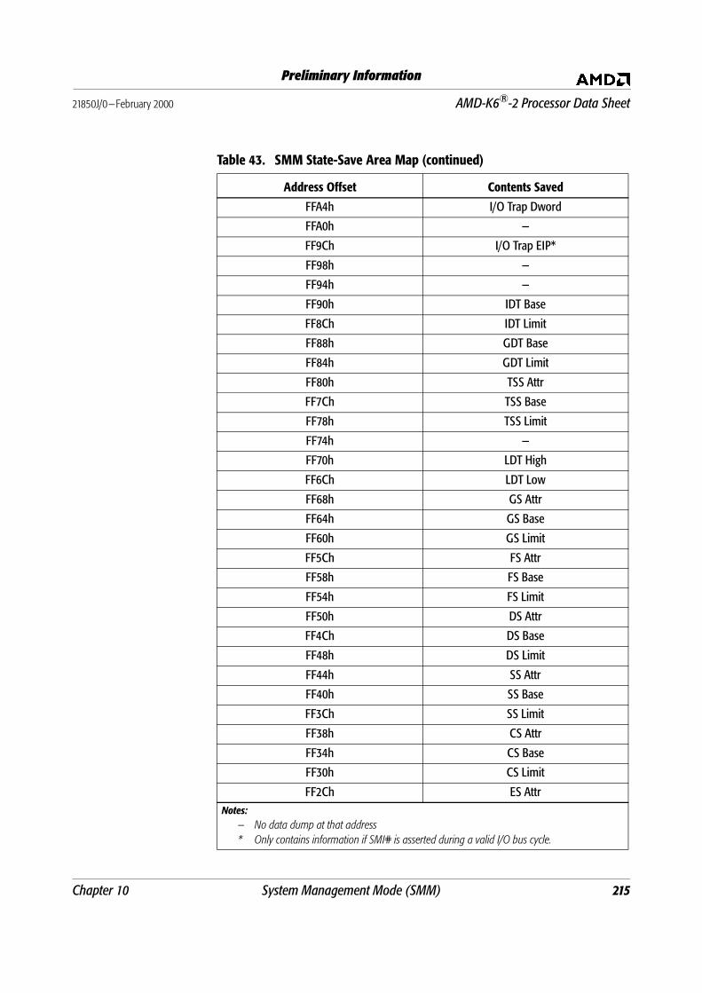
Chapter 10 System Management Mode (SMM) 215
21850J/0—February 2000 AMD-K6®-2 Processor Data Sheet
Preliminary Information
FFA4h I/O Trap Dword
FFA0h —
FF9Ch I/O Trap EIP*
FF98h —
FF94h —
FF90h IDT Base
FF8Ch IDT Limit
FF88h GDT Base
FF84h GDT Limit
FF80h TSS Attr
FF7Ch TSS Base
FF78h TSS Limit
FF74h —
FF70h LDT High
FF6Ch LDT Low
FF68h GS Attr
FF64h GS Base
FF60h GS Limit
FF5Ch FS Attr
FF58h FS Base
FF54h FS Limit
FF50h DS Attr
FF4Ch DS Base
FF48h DS Limit
FF44h SS Attr
FF40h SS Base
FF3Ch SS Limit
FF38h CS Attr
FF34h CS Base
FF30h CS Limit
FF2Ch ES Attr
Table 43. SMM State-Save Area Map (continued)
Address Offset Contents Saved
Notes:
— No data dump at that address
* Only contains information if SMI# is asserted during a valid I/O bus cycle.

216 System Management Mode (SMM) Chapter 10
AMD-K6®-2 Processor Data Sheet 21850J/0—February 2000
Preliminary Information
10.4 SMM Revision Identifier
The SMM revision identifier at offset FEFCh in the SMM
state-save area specifies the version of SMM and the extensions
that are available on the processor. The SMM revision identifier
fields are as follows:
Bits 31–18—Reserved
Bit 17—SMM base address relocation (1 = enabled)
Bit 16—I/O trap restart (1 = enabled)
Bits 15–0—SMM revision level for the AMD-K6-2 processor
= 0002h
FF28h ES Base
FF24h ES Limit
FF20h —
FF1Ch —
FF18h —
FF14h CR2
FF10h CR4
FF0Ch I/O Restart ESI*
FF08h I/O Restart ECX*
FF04h I/O Restart EDI*
FF02h HALT Restart Slot
FF00h I/O Trap Restart Slot
FEFCh SMM RevID
FEF8h SMM Base
FEF7h–FE00h —
Table 43. SMM State-Save Area Map (continued)
Address Offset Contents Saved
Notes:
— No data dump at that address
* Only contains information if SMI# is asserted during a valid I/O bus cycle.

Chapter 10 System Management Mode (SMM) 217
21850J/0—February 2000 AMD-K6®-2 Processor Data Sheet
Preliminary Information
Table 44 shows the format of the SMM Revision Identifier.
10.5 SMM Base Address
During RESET, the processor sets the base address of the
code-segment (CS) for the SMM memory area—the SMM base
address—to its default, 0003_0000h. The SMM base address at
offset FEF8h in the SMM state-save area can be changed by the
SMM service routine to any address that is aligned to a
32-Kbyte boundary. (Locations not aligned to a 32-Kbyte
boundary cause the processor to enter the Shutdown state when
executing the RSM instruction.)
In some operating environments it may be desirable to relocate
the 64-Kbyte SMM memory area to a high memory area in order
to provide more low memory for legacy software. During system
initialization, the base of the 64-Kbyte SMM memory area is
relocated by the BIOS. To relocate the SMM base address, the
system enters the SMM handler at the default address. This
handler changes the SMM base address location in the SMM
state-save area, copies the SMM handler to the new location,
and exits SMM.
The next time SMM is entered, the processor saves its state at
the new base address. This new address is used for every SMM
entry until the SMM base address in the SMM state-save area is
changed or a hardware reset occurs.
10.6 Halt Restart Slot
During entry into SMM, the halt restart slot at offset FF02h in
the SMM state-save area indicates if SMM was entered from the
Halt state. Before returning from SMM, the halt restart slot
(offset FF02h) can be written to by the SMM service routine to
specify whether the return from SMM takes the processor back
to the Halt state or to the next instruction after the HLT
instruction.
Table 44. SMM Revision Identifier
31–18 17 16 15–0
Reserved SMM Base Relocation I/O Trap Extension SMM Revision Level
0 1 1 0002h
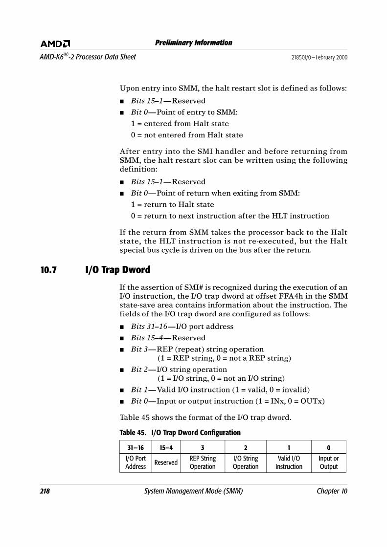
218 System Management Mode (SMM) Chapter 10
AMD-K6®-2 Processor Data Sheet 21850J/0—February 2000
Preliminary Information
Upon entry into SMM, the halt restart slot is defined as follows:
Bits 15–1—Reserved
Bit 0—Point of entry to SMM:
1 = entered from Halt state
0 = not entered from Halt state
After entry into the SMI handler and before returning from
SMM, the halt restart slot can be written using the following
definition:
Bits 15–1—Reserved
Bit 0—Point of return when exiting from SMM:
1 = return to Halt state
0 = return to next instruction after the HLT instruction
If the return from SMM takes the processor back to the Halt
state, the HLT instruction is not re-executed, but the Halt
special bus cycle is driven on the bus after the return.
10.7 I/O Trap Dword
If the assertion of SMI# is recognized during the execution of an
I/O instruction, the I/O trap dword at offset FFA4h in the SMM
state-save area contains information about the instruction. The
fields of the I/O trap dword are configured as follows:
Bits 31–16—I/O port address
Bits 15–4—Reserved
Bit 3—REP (repeat) string operation
(1 = REP string, 0 = not a REP string)
Bit 2—I/O string operation
(1 = I/O string, 0 = not an I/O string)
Bit 1—Valid I/O instruction (1 = valid, 0 = invalid)
Bit 0—Input or output instruction (1 = INx, 0 = OUTx)
Table 45 shows the format of the I/O trap dword.
Table 45. I/O Trap Dword Configuration
31—16 15—4 3 2 1 0
I/O Port Address
ReservedREP StringOperation
I/O String Operation
Valid I/O Instruction
Input or Output

Chapter 10 System Management Mode (SMM) 219
21850J/0—February 2000 AMD-K6®-2 Processor Data Sheet
Preliminary Information
The I/O trap dword is related to the I/O trap restart slot (see “I/O
Trap Restart Slot”). If bit 1 of the I/O trap dword is set by the
processor, it means that SMI# was asserted during the
execution of an I/O instruction. The SMI handler tests bit 1 to
see if there is a valid I/O instruction trapped. If the I/O
instruction is valid, the SMI handler is required to ensure the
I/O trap restart slot is set properly. The I/O trap restart slot
informs the processor whether it should re-execute the I/O
instruction after the RSM or execute the instruction following
the trapped I/O instruction.
Note: If SMI# is sampled asserted during an I/O bus cycle a
minimum of three clock edges before BRDY# is sampled
asserted, the associated I/O instruction is guaranteed to be
trapped by the SMI handler.
10.8 I/O Trap Restart Slot
The I/O trap restart slot at offset FF00h in the SMM state-save
area specifies whether the trapped I/O instruction should be
re-executed on return from SMM. This slot in the state-save area
is called the I/O instruction restart function. Re-executing a
trapped I/O instruction is useful, for example, if an I/O write
occurs to a disk that is powered down. The system logic
monitoring such an access can assert SMI#. Then the SMM
service routine would query the system logic, detect a failed I/O
write, take action to power-up the I/O device, enable the I/O
trap restart slot feature, and return from SMM.
The fields of the I/O trap restart slot are defined as follows:
Bits 31–16—Reserved
Bits 15–0—I/O instruction restart on return from SMM:
0000h = execute the next instruction after the trapped
I/O instruction
00FFh = re-execute the trapped I/O instruction
Table 46 shows the format of the I/O trap restart slot.
Table 46. I/O Trap Restart Slot
31–16 15–0
Reserved
I/O Instruction restart on return from SMM:
0000h = execute the next instruction after the trapped I/O
00FFh = re-execute the trapped I/O instruction

220 System Management Mode (SMM) Chapter 10
AMD-K6®-2 Processor Data Sheet 21850J/0—February 2000
Preliminary Information
The processor initializes the I/O trap restart slot to 0000h upon
entry into SMM. If SMM was entered due to a trapped I/O
instruction, the processor indicates the validity of the I/O
instruction by setting or clearing bit 1 of the I/O trap dword at
offset FFA4h in the SMM state-save area. The SMM service
routine should test bit 1 of the I/O trap dword to determine if a
valid I/O instruction was being executed when entering SMM
and before writing the I/O trap restart slot. If the I/O instruction
is valid, the SMM service routine can safely rewrite the I/O trap
restart slot with the value 00FFh, which causes the processor to
re-execute the trapped I/O instruction when the RSM
instruction is executed. If the I/O instruction is invalid, writing
the I/O trap restart slot has undefined results.
If a second SMI# is asserted and a valid I/O instruction was
trapped by the first SMM handler, the processor services the
second SMI# prior to re-executing the trapped I/O instruction.
The second entry into SMM never has bit 1 of the I/O trap dword
set, and the second SMM service routine must not rewrite the
I/O trap restart slot.
During a simultaneous SMI# I/O instruction trap and debug
breakpoint trap, the AMD-K6-2 processor first responds to the
SMI# and postpones recognizing the debug exception until
after returning from SMM via the RSM instruction. If the debug
registers DR3–DR0 are used while in SMM, they must be saved
and restored by the SMM handler. The processor automatically
saves and restores DR7–DR6. If the I/O trap restart slot in the
SMM state-save area contains the value 00FFh when the RSM
instruction is executed, the debug trap does not occur until
after the I/O instruction is re-executed.
10.9 Exceptions, Interrupts, and Debug in SMM
During an SMI# I/O trap, the exception/interrupt priority of the
AMD-K6-2 processor changes from its normal priority. The
normal priority places the debug traps at a priority higher than
the sampling of the FLUSH# or SMI# signals. However, during
an SMI# I/O trap, the sampling of the FLUSH# or SMI# signals
takes precedence over debug traps.
The processor recognizes the assertion of NMI within SMM
immediately after the completion of an IRET instruction. Once
NMI is recognized within SMM, NMI recognition remains
enabled until SMM is exited, at which point NMI masking is
restored to the state it was in before entering SMM.

Chapter 11 Test and Debug 221
21850J/0—February 2000 AMD-K6®-2 Processor Data Sheet
Preliminary Information
11 Test and Debug
The AMD-K6-2 processor implements various test and debug
modes to enable the functional and manufacturing testing of
systems and boards that use the processor. In addition, the
debug features of the processor allow designers to debug the
instruction execution of software components. This chapter
describes the following test and debug features:
Built-In Self-Test (BIST)—The BIST, which is invoked after
the falling transition of RESET, runs internal tests that
exercise most on-chip RAM structures.
Tri-State Test Mode—A test mode that causes the processor
to float its output and bidirectional pins.
Boundary-Scan Test Access Port (TAP)—The Joint Test Action
Group (JTAG) test access function defined by the IEEE
Standard Test Access Port and Boundary-Scan Architecture
(IEEE 1149.1-1990) specification.
Level-One (L1) Cache Inhibit—A feature that disables the
processor’s internal L1 instruction and data caches.
Debug Support—Consists of all x86-compatible software
debug features, including the debug extensions.
11.1 Built-In Self-Test (BIST)
Following the falling transition of RESET, the processor
unconditionally runs its BIST. The internal resources tested
during BIST include the following:
L1 instruction and data caches
Instruction and Data Translation Lookaside Buffers (TLBs)
The contents of the EAX general-purpose register after the
completion of reset indicate if the BIST was successful. If EAX
contains 0000_0000h, then BIST was successful. If EAX is
non-zero, the BIST failed. Following the completion of the BIST,
the processor jumps to address FFFF_FFF0h to start
instruction execution, regardless of the outcome of the BIST.
The BIST takes approximately 295,000 processor clocks to
complete.
222 Test and Debug Chapter 11
AMD-K6®-2 Processor Data Sheet 21850J/0—February 2000
Preliminary Information
11.2 Tri-State Test Mode
The Tri-State Test mode causes the processor to float its output
and bidirectional pins, which is useful for board-level
manufacturing testing. In this mode, the processor is
electrically isolated from other components on a system board,
allowing automated test equipment (ATE) to test components
that drive the same signals as those the processor floats.
If the FLUSH# signal is sampled Low during the falling
transition of RESET, the processor enters the Tri-State Test
mode. (See “FLUSH# (Cache Flush)” on page 103 for the
specific sampling requirements.) The signals floated in the
Tri-State Test mode are as follows:
The VCC2DET, VCC2H/L#, and TDO signals are the only
outputs not floated in the Tri-State Test mode. VCC2DET and
VCC2H/L# must remain Low to ensure the system continues to
supply the specified processor core voltage to the VCC2 pins.
TDO is never floated because the Boundary-Scan Test Access
Port must remain enabled at all times, including during the
Tri-State Test mode.
The Tri-State Test mode is exited when the processor samples
RESET asserted.
A[31:3] D/C# M/IO#
ADS# D[63:0] PCD
ADSC# DP[7:0] PCHK#
AP FERR# PWT
APCHK# HIT# SCYC
BE[7:0]# HITM# SMIACT#
BREQ HLDA W/R#
CACHE# LOCK#

Chapter 11 Test and Debug 223
21850J/0—February 2000 AMD-K6®-2 Processor Data Sheet
Preliminary Information
11.3 Boundary-Scan Test Access Port (TAP)
The boundary-scan Test Access Port (TAP) is an IEEE standard
that defines synchronous scanning test methods for complex
logic circuits, such as boards containing a processor. The
AMD-K6-2 processor supports the TAP standard defined in the
IEEE Standard Test Access Port and Boundary-Scan Architecture
(IEEE 1149.1-1990) specification.
Boundary scan testing uses a shift register consisting of the
serial interconnection of boundary-scan cells that correspond to
each I/O buffer of the processor. This non-inverting register
chain, called a Boundary Scan Register (BSR), can be used to
capture the state of every processor pin and to drive every
processor output and bidirectional pin to a known state.
Each BSR of every component on a board that implements the
boundary-scan architecture can be serially interconnected to
enable component interconnect testing.
Test Access Port The TAP consists of the following:
Test Access Port (TAP) Controller—The TAP controller is a
synchronous, finite state machine that uses the TMS and
TDI input signals to control a sequence of test operations.
See “TAP Controller State Machine” on page 232 for a list
of TAP states and their definition.
Instruction Register (IR)—The IR contains the instructions
that select the test operation to be performed and the Test
Data Register (TDR) to be selected. See “TAP Registers” on
page 224 for more details on the IR.
Test Data Registers (TDR)—The three TDRs are used to
process the test data. Each TDR is selected by an
instruction in the Instruction Register (IR). See “TAP
Registers” on page 224 for a list of these registers and their
functions.
TAP Signals The test signals associated with the TAP controller are as
follows:
TCK—The Test Clock for all TAP operations. The rising edge
of TCK is used for sampling TAP signals, and the falling
edge of TCK is used for asserting TAP signals. The state of
the TMS signal sampled on the rising edge of TCK causes

224 Test and Debug Chapter 11
AMD-K6®-2 Processor Data Sheet 21850J/0—February 2000
Preliminary Information
the state transitions of the TAP controller to occur. TCK can
be stopped in the logic 0 or 1 state.
TDI—The Test Data Input represents the input to the most
significant bit of all TAP registers, including the IR and all
test data registers. Test data and instructions are serially
shifted by one bit into their respective registers on the rising
edge of TCK.
TDO—The Test Data Output represents the output of the
least significant bit of all TAP registers, including the IR and
all test data registers. Test data and instructions are serially
shifted by one bit out of their respective registers on the
falling edge of TCK.
TMS—The Test Mode Select input specifies the test
function and sequence of state changes for boundary-scan
testing. If TMS is sampled High for five or more consecutive
clocks, the TAP controller enters its reset state.
TRST#—The Test Reset signal is an asynchronous reset that
unconditionally causes the TAP controller to enter its reset
state.
Refer to “Electrical Data” on page 253 and “Signal Switching
Characteristics” on page 267 to obtain the electrical
specifications of the test signals.
TAP Registers The AMD-K6-2 processor provides an Instruction Register (IR)
and three Test Data Registers (TDR) to support the
boundary-scan architecture. The IR and one of the TDRs—the
Boundary-Scan Register (BSR)—consist of a shift register and
an output register. The shift register is loaded in parallel in the
Capture states. (See “TAP Controller State Machine” on page
232 for a description of the TAP controller states.) In addition,
the shift register is loaded and shifted serially in the Shift
states. The output register is loaded in parallel from its
corresponding shift register in the Update states.
Instruction Register (IR). The IR is a 5-bit register, without parity,
that determines which instruction to run and which test data
register to select. When the TAP controller enters the
Capture-IR state, the processor loads the following bits into the
IR shift register:
01b—Loaded into the two least significant bits, as specified
by the IEEE 1149.1 standard
000b—Loaded into the three most significant bits

Chapter 11 Test and Debug 225
21850J/0—February 2000 AMD-K6®-2 Processor Data Sheet
Preliminary Information
Loading 00001b into the IR shift register during the Capture-IR
state results in loading the SAMPLE/PRELOAD instruction.
For each entry into the Shift-IR state, the IR shift register is
serially shifted by one bit toward the TDO pin. During the shift,
the most significant bit of the IR shift register is loaded from
the TDI pin.
The IR output register is loaded from the IR shift register in the
Update-IR state, and the current instruction is defined by the IR
output register. See “TAP Instructions” on page 231 for a list and
definition of the instructions supported by the AMD-K6-2
processor.
Boundary Scan Register (BSR). The BSR is a Test Data Register
consisting of the interconnection of 152 boundary-scan cells.
Each output and bidirectional pin of the processor requires a
two-bit cell, where one bit corresponds to the pin and the other
bit is the output enable for the pin. When a 0 is shifted into the
enable bit of a cell, the corresponding pin is floated, and when a
1 is shifted into the enable bit, the pin is driven valid. Each
input pin requires a one-bit cell that corresponds to the pin. The
last cell of the BSR is reserved and does not correspond to any
processor pin.
The total number of bits that comprise the BSR is 281. The
order of the bits in the BSR differs between the Model 8/[7:0]
and the Model 8/[F:8] processors. Table 47 on page 227 and
Table 48 on page 229 list the order of these bits, respectively,
where TDI is the input to bit 280, and TDO is driven from the
output of bit 0. The entries listed as pin_E (where pin is an
output or bidirectional signal) are the enable bits.
If the BSR is the register selected by the current instruction
and the TAP controller is in the Capture-DR state, the processor
loads the BSR shift register as follows:
If the current instruction is SAMPLE/PRELOAD, then the
current state of each input, output, and bidirectional pin is
loaded. A bidirectional pin is treated as an output if its
enable bit equals 1, and it is treated as an input if its enable
bit equals 0.
If the current instruction is EXTEST, then the current state
of each input pin is loaded. A bidirectional pin is treated as
an input, regardless of the state of its enable.

226 Test and Debug Chapter 11
AMD-K6®-2 Processor Data Sheet 21850J/0—February 2000
Preliminary Information
While in the Shift-DR state, the BSR shift register is serially
shifted toward the TDO pin. During the shift, bit 280 of the BSR
is loaded from the TDI pin.
The BSR output register is loaded with the contents of the BSR
shift register in the Update-DR state. If the current instruction
is EXTEST, the processor’s output pins, as well as those
bidirectional pins that are enabled as outputs, are driven with
their corresponding values from the BSR output register.

Chapter 11 Test and Debug 227
21850J/0—February 2000 AMD-K6®-2 Processor Data Sheet
Preliminary Information
Table 47. Boundary Scan Bit Definitions for Model 8/[7:0]
Bit Pin/Enable Bit Pin/Enable Bit Pin/Enable Bit Pin/Enable Bit Pin/Enable Bit Pin/Enable
280 D35_E 247 D21 214 D4_E 181 A3 148 A20 115 A16
279 D35 246 D18_E 213 D4 180 A31_E 147 A13_E 114 FERR_E
278 D29_E 245 D18 212 DP0_E 179 A31 146 A13 113 FERR#
277 D29 244 D19_E 211 DP0 178 A21_E 145 DP7_E 112 HIT_E
276 D33_E 243 D19 210 HOLD 177 A21 144 DP7 111 HIT#
275 D33 242 D16_E 209 BOFF# 176 A30_E 143 BE6_E 110 BE7_E
274 D27_E 241 D16 208 AHOLD 175 A30 142 BE6# 109 BE7#
273 D27 240 D17_E 207 STPCLK# 174 A7_E 141 A12_E 108 NA#
272 DP3_E 239 D17 206 INIT 173 A7 140 A12 107 ADSC_E
271 DP3 238 D15_E 205 IGNNE# 172 A24_E 139 CLK 106 ADSC#
270 D25_E 237 D15 204 BF1 171 A24 138 BE4_E 105 BE5_E
269 D25 236 DP1_E 203 BF2 170 A18_E 137 BE4# 104 BE5#
268 D0_E 235 DP1 202 RESET 169 A18 136 A10_E 103 WB/WT#
267 D0 234 D13_E 201 BF0 168 A5_E 135 A10 102 PWT_E
266 D30_E 233 D13 200 FLUSH# 167 A5 134 D63_E 101 PWT
265 D30 232 D6_E 199 INTR 166 A22_E 133 D63 100 BE3_E
264 DP2_E 231 D6 198 NMI 165 A22 132 BE2_E 99 BE3#
263 DP2 230 D14_E 197 SMI# 164 EADS# 131 BE2# 98 BREQ_E
262 D2_E 229 D14 196 A25_E 163 A4_E 130 A15_E 97 BREQ
261 D2 228 D11_E 195 A25 162 A4 129 A15 96 PCD_E
260 D28_E 227 D11 194 A23_E 161 HITM_E 128 BRDY# 95 PCD
259 D28 226 D1_E 193 A23 160 HITM# 127 BE1_E 94 WR_E
258 D24_E 225 D1 192 A26_E 159 A9_E 126 BE1# 93 W/R#
257 D24 224 D12_E 191 A26 158 A9 125 A14_E 92 SMIACT_E
256 D26_E 223 D12 190 A29_E 157 SCYC_E 124 A14 91 SMIACT#
255 D26 222 D10_E 189 A29 156 SCYC 123 BRDYC# 90 EWBE#
254 D22_E 221 D10 188 A28_E 155 A8_E 122 BE0_E 89 DC_E
253 D22 220 D7_E 187 A28 154 A8 121 BE0# 88 D/C#
252 D23_E 219 D7 186 A27_E 153 A19_E 120 A17_E 87 APCHK_E
251 D23 218 D8_E 185 A27 152 A19 119 A17 86 APCHK#
250 D20_E 217 D8 184 A11_E 151 A6_E 118 KEN# 85 CACHE_E
249 D20 216 D9_E 183 A11 150 A6 117 A20M# 84 CACHE#
248 D21_E 215 D9 182 A3_E 149 A20_E 116 A16_E 83 ADS_E

228 Test and Debug Chapter 11
AMD-K6®-2 Processor Data Sheet 21850J/0—February 2000
Preliminary Information
82 ADS# 68 DP6_E 54 D53_E 40 D43_E 26 D38_E 12 D3_E
81 AP_E 67 DP6 53 D53 39 D43 25 D38 11 D3
80 AP 66 D54_E 52 D47_E 38 D62_E 24 D58_E 10 D39_E
79 INV 65 D54 51 D47 37 D62 23 D58 9 D39
78 HLDA_E 64 D50_E 50 D59_E 36 D49_E 22 D42_E 8 D32_E
77 HLDA 63 D50 49 D59 35 D49 21 D42 7 D32
76 PCHK_E 62 D56_E 48 D51_E 34 DP4_E 20 D36_E 6 D5_E
75 PCHK# 61 D56 47 D51 33 DP4 19 D36 5 D5
74 LOCK_E 60 D55_E 46 D45_E 32 D46_E 18 D60_E 4 D37_E
73 LOCK# 59 D55 45 D45 31 D46 17 D60 3 D37
72 MIO_E 58 D48_E 44 D61_E 30 D41_E 16 D40_E 2 D31_E
71 M/IO# 57 D48 43 D61 29 D41 15 D40 1 D31
70 D52_E 56 D57_E 42 DP5_E 28 D44_E 14 D34_E 0 Reserved
69 D52 55 D57 41 DP5 27 D44 13 D34
Table 47. Boundary Scan Bit Definitions for Model 8/[7:0] (continued)
Bit Pin/Enable Bit Pin/Enable Bit Pin/Enable Bit Pin/Enable Bit Pin/Enable Bit Pin/Enable

Chapter 11 Test and Debug 229
21850J/0—February 2000 AMD-K6®-2 Processor Data Sheet
Preliminary Information
Table 48. Boundary Scan Bit Definitions for Model 8/[F:8]
Bit Pin/Enable Bit Pin/Enable Bit Pin/Enable Bit Pin/Enable Bit Pin/Enable Bit Pin/Enable
280 D35_E 247 D19 214 BF1 181 A24 148 A14 115 BE7#
279 D35 246 D16_E 213 BF2 180 A18_E 147 A17_E 114 PCD_E
278 D29_E 245 D16 212 RESET 179 A18 146 A17 113 PCD
277 D29 244 D17_E 211 BF0 178 A5_E 145 A16_E 112 DC_E
276 D33_E 243 D17 210 FLUSH# 177 A5 144 A16 111 D/C#
275 D33 242 D15_E 209 INTR 176 EADS# 143 HIT_E 110 WR_E
274 D27_E 241 D15 208 NMI 175 A22_E 142 HIT# 109 W/R#
273 D27 240 DP1_E 207 SMI# 174 A22 141 ADS_E 108 NA#
272 DP0_E 239 DP1 206 A25_E 173 AHOLD 140 ADS# 107 PWT_E
271 DP0 238 D13_E 205 A25 172 HITM_E 139 CLK 106 PWT
270 DP3_E 237 D13 204 A26_E 171 HITM# 138 ADSC_E 105 CACHE_E
269 DP3 236 D6_E 203 A26 170 A4_E 137 ADSC# 104 CACHE#
268 D25_E 235 D6 202 A29_E 169 A4 136 BE0_E 103 WB/WT#
267 D25 234 D14_E 201 A29 168 A9_E 135 BE0# 102 MIO_E
266 D0_E 233 D14 200 A28_E 167 A9 134 AP_E 101 M/IO#
265 D0 232 D11_E 199 A28 166 A8_E 133 AP 100 BREQ_E
264 D30_E 231 D11 198 A23_E 165 A8 132 BE1_E 99 BREQ
263 D30 230 D1_E 197 A23 164 A19_E 131 BE1# 98 SCYC_E
262 DP2_E 229 D1 196 A27_E 163 A19 130 BE2_E 97 SCYC
261 DP2 228 D12_E 195 A27 162 BOFF# 129 BE2# 96 LOCK_E
260 D2_E 227 D12 194 A11_E 161 A6_E 128 BRDY# 95 LOCK#
259 D2 226 D10_E 193 A11 160 A6 127 BE3_E 94 APCHK_E
258 D28_E 225 D10 192 A3_E 159 A20_E 126 BE3# 93 APCHK#
257 D28 224 D7_E 191 A3 158 A20 125 BE4_E 92 PCHK_E
256 D24_E 223 D7 190 A31_E 157 A13_E 124 BE4# 91 PCHK#
255 D24 222 D8_E 189 A31 156 A13 123 BRDYC# 90 EWBE#
254 D26_E 221 D8 188 A21_E 155 A12_E 122 BE5_E 89 SMIACT_E
253 D26 220 D9_E 187 A21 154 A12 121 BE5# 88 SMIACT#
252 D21_E 219 D9 186 A30_E 153 A10_E 120 BE6_E 87 FERR_E
251 D21 218 HOLD 185 A30 152 A10 119 BE6# 86 FERR#
250 D18_E 217 STPCLK# 184 A7_E 151 A15_E 118 KEN# 85 D20_E
249 D18 216 INIT 183 A7 150 A15 117 INV 84 D20
248 D19_E 215 IGNNE# 182 A24_E 149 A14_E 116 BE7_E 83 D22_E
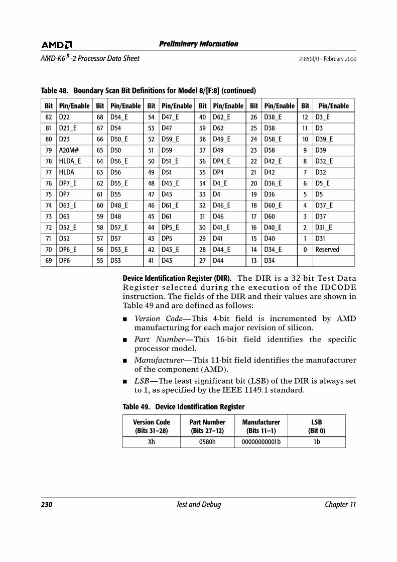
230 Test and Debug Chapter 11
AMD-K6®-2 Processor Data Sheet 21850J/0—February 2000
Preliminary Information
Device Identification Register (DIR). The DIR is a 32-bit Test Data
Register selected during the execution of the IDCODE
instruction. The fields of the DIR and their values are shown in
Table 49 and are defined as follows:
Version Code—This 4-bit field is incremented by AMD
manufacturing for each major revision of silicon.
Part Number—This 16-bit field identifies the specific
processor model.
Manufacturer—This 11-bit field identifies the manufacturer
of the component (AMD).
LSB—The least significant bit (LSB) of the DIR is always set
to 1, as specified by the IEEE 1149.1 standard.
82 D22 68 D54_E 54 D47_E 40 D62_E 26 D38_E 12 D3_E
81 D23_E 67 D54 53 D47 39 D62 25 D38 11 D3
80 D23 66 D50_E 52 D59_E 38 D49_E 24 D58_E 10 D39_E
79 A20M# 65 D50 51 D59 37 D49 23 D58 9 D39
78 HLDA_E 64 D56_E 50 D51_E 36 DP4_E 22 D42_E 8 D32_E
77 HLDA 63 D56 49 D51 35 DP4 21 D42 7 D32
76 DP7_E 62 D55_E 48 D45_E 34 D4_E 20 D36_E 6 D5_E
75 DP7 61 D55 47 D45 33 D4 19 D36 5 D5
74 D63_E 60 D48_E 46 D61_E 32 D46_E 18 D60_E 4 D37_E
73 D63 59 D48 45 D61 31 D46 17 D60 3 D37
72 D52_E 58 D57_E 44 DP5_E 30 D41_E 16 D40_E 2 D31_E
71 D52 57 D57 43 DP5 29 D41 15 D40 1 D31
70 DP6_E 56 D53_E 42 D43_E 28 D44_E 14 D34_E 0 Reserved
69 DP6 55 D53 41 D43 27 D44 13 D34
Table 48. Boundary Scan Bit Definitions for Model 8/[F:8] (continued)
Bit Pin/Enable Bit Pin/Enable Bit Pin/Enable Bit Pin/Enable Bit Pin/Enable Bit Pin/Enable
Table 49. Device Identification Register
Version Code(Bits 31–28)
Part Number(Bits 27–12)
Manufacturer(Bits 11–1)
LSB(Bit 0)
Xh 0580h 00000000001b 1b

Chapter 11 Test and Debug 231
21850J/0—February 2000 AMD-K6®-2 Processor Data Sheet
Preliminary Information
Bypass Register (BR). The BR is a Test Data Register consisting of
a 1-bit shift register that provides the shortest path between
TDI and TDO. When the processor is not involved in a test
operation, the BR can be selected by an instruction to allow the
transfer of test data through the processor without having to
serially scan the test data through the BSR. This functionality
preserves the state of the BSR and significantly reduces test
time.
The BR register is selected by the BYPASS and HIGHZ
instructions as well as by any instructions not supported by the
AMD-K6-2 processor.
TAP Instructions The processor supports the three instructions required by the
IEEE 1149.1 standard—EXTEST, SAMPLE/PRELOAD, and
BYPASS—as well as two additional optional instructions—
IDCODE and HIGHZ.
Table 50 shows the complete set of TAP instructions supported
by the processor along with the 5-bit Instruction Register
encoding and the register selected by each instruction.
EXTEST. When the EXTEST instruction is executed, the
processor loads the BSR shift register with the current state of
the input and bidirectional pins in the Capture-DR state and
drives the output and bidirectional pins with the corresponding
values from the BSR output register in the Update-DR state.
Table 50. Supported Tap Instructions
Instruction Encoding Register Description
EXTEST1 00000b BSR Sample inputs and drive outputs
SAMPLE / PRELOAD 00001b BSR Sample inputs and outputs, then load the BSR
IDCODE 00010b DIR Read DIR
HIGHZ 00011b BR Float outputs and bidirectional pins
BYPASS2 00100b–11110b BR Undefined instruction, execute the BYPASS instruction
BYPASS3 11111b BR Connect TDI to TDO to bypass the BSR
Notes:
1. Following the execution of the EXTEST instruction, the processor must be reset in order to return to normal, non-test operation.
2. These instruction encodings are undefined on the AMD-K6-2 processor and default to the BYPASS instruction.
3. Because the TDI input contains an internal pullup, the BYPASS instruction is executed if the TDI input is not connected or openduring an instruction scan operation. The BYPASS instruction does not affect the normal operational state of the processor.

232 Test and Debug Chapter 11
AMD-K6®-2 Processor Data Sheet 21850J/0—February 2000
Preliminary Information
SAMPLE/PRELOAD. The SAMPLE/PRELOAD instruction performs
two functions. These functions are as follows:
During the Capture-DR state, the processor loads the BSR
shift register with the current state of every input, output,
and bidirectional pin.
During the Update-DR state, the BSR output register is
loaded from the BSR shift register in preparation for the
next EXTEST instruction.
The SAMPLE/PRELOAD instruction does not affect the normal
operational state of the processor.
BYPASS. The BYPASS instruction selects the BR register, which
reduces the boundary-scan length through the processor from
281 to one (TDI to BR to TDO). The BYPASS instruction does
not affect the normal operational state of the processor.
IDCODE. The IDCODE instruction selects the DIR register,
allowing the device identification code to be shifted out of the
processor. This instruction is loaded into the IR when the TAP
controller is reset. The IDCODE instruction does not affect the
normal operational state of the processor.
HIGHZ. The HIGHZ instruct ion forces a l l output and
bidirectional pins to be floated. During this instruction, the BR
is selected and the normal operational state of the processor is
not affected.
TAP Controller State Machine
The TAP controller state diagram is shown in Figure 86 on page
233. State transitions occur on the rising edge of TCK. The logic
0 or 1 next to the states represents the value of the TMS signal
sampled by the processor on the rising edge of TCK.

Chapter 11 Test and Debug 233
21850J/0—February 2000 AMD-K6®-2 Processor Data Sheet
Preliminary Information
Figure 86. TAP State Diagram
Test-Logic-Reset
Shift-DR
Pause-DR
Update-DR Update-IR
0
1
0
0
0
0
0
1 1
11 1
0
0
0
0
0
1 1
0 0
1 1
0
1 1
0
0
1
1 1
1
Run-Test/Idle
Exit2-IR
Exit1-IR
Pause-IR
Shift-IR
Select-DR-Scan Select-IR-Scan
Capture-DR Capture-IR
Exit1-DR
Exit2-DR
IEEE Std 1149.1-1990, Copyright © 1990. IEEE. All rights reserved

234 Test and Debug Chapter 11
AMD-K6®-2 Processor Data Sheet 21850J/0—February 2000
Preliminary Information
The states of the TAP controller are described as follows:
Test-Logic-Reset. This state represents the initial reset state of the
TAP controller and is entered when the processor samples
RESET asserted, when TRST# is asynchronously asserted, and
when TMS is sampled High for five or more consecutive clocks.
In addition, this state can be entered from the Select-IR-Scan
state. The IR is initialized with the IDCODE instruction, and
the processor’s normal operation is not affected in this state.
Capture-DR. During the SAMPLE/PRELOAD instruction, the
processor loads the BSR shift register with the current state of
every input, output, and bidirectional pin. During the EXTEST
instruction, the processor loads the BSR shift register with the
current state of every input and bidirectional pin.
Capture-IR. When the TAP controller enters the Capture-IR state,
the processor loads 01b into the two least significant bits of the
IR shift register and loads 000b into the three most significant
bits of the IR shift register.
Shift-DR. While in the Shift-DR state, the selected TDR shift
register is serially shifted toward the TDO pin. During the shift,
the most significant bit of the TDR is loaded from the TDI pin.
Shift-IR. While in the Shift-IR state, the IR shift register is
serially shifted toward the TDO pin. During the shift, the most
significant bit of the IR is loaded from the TDI pin.
Update-DR. During the SAMPLE/PRELOAD instruction, the BSR
output register is loaded with the contents of the BSR shift
register. During the EXTEST instruction, the output pins, as
well as those bidirectional pins defined as outputs, are driven
with their corresponding values from the BSR output register.
Update-IR. In this state, the IR output register is loaded from the
IR shift register, and the current instruction is defined by the
IR output register.

Chapter 11 Test and Debug 235
21850J/0—February 2000 AMD-K6®-2 Processor Data Sheet
Preliminary Information
The following states have no effect on the normal or test
operation of the processor other than as shown in Figure 86 on
page 233:
Run-Test/Idle—This state is an idle state between scan
operations.
Select-DR-Scan—This is the initial state of the test data
register state transitions.
Select-IR-Scan—This is the initial state of the Instruction
Register state transitions.
Exit1-DR—This state is entered to terminate the shifting
process and enter the Update-DR state.
Exit1-IR—This state is entered to terminate the shifting
process and enter the Update-IR state.
Pause-DR—This state is entered to temporarily stop the
shifting process of a Test Data Register.
Pause-IR—This state is entered to temporarily stop the
shifting process of the Instruction Register.
Exit2-DR—This state is entered in order to either terminate
the shifting process and enter the Update-DR state or to
resume shifting following the exit from the Pause-DR state.
Exit2-IR—This state is entered in order to either terminate
the shifting process and enter the Update-IR state or to
resume shifting following the exit from the Pause-IR state.
11.4 L1 Cache Inhibit
Purpose The AMD-K6-2 processor provides a means for inhibiting the
normal operation of its L1 instruction and data caches while
still supporting an external cache. This capability allows system
designers to disable the L1 cache during the testing and debug
of an external cache.
If the Cache Inhibit bit (bit 3) of Test Register 12 (TR12) is set
to 0, the processor’s L1 cache is enabled and operates as
described in “Cache Organization” on page 179. If the Cache
Inhibit bit is set to 1, the L1 cache is disabled and no new cache
lines are allocated. Even though new allocations do not occur,
valid L1 cache lines remain valid and are read by the processor
when a requested address hits a cache line. In addition, the
processor continues to support inquire cycles initiated by the

236 Test and Debug Chapter 11
AMD-K6®-2 Processor Data Sheet 21850J/0—February 2000
Preliminary Information
system logic, including the execution of writeback cycles when
a modified cache line is hit.
While the L1 is inhibited, the processor continues to drive the
PCD output signal appropriately, which system logic can use to
control external caching.
In order to completely disable the L1 cache so no valid lines
exist in the cache, the Cache Inhibit bit must be set to 1 and the
cache must be flushed in one of the following ways:
Asserting the FLUSH# input signal
Executing the WBINVD instruction
Executing the INVD instruction (modified cache lines are
not written back to memory)
Make use of the Page Flush/Invalidate Register (PFIR)
(AMD-K6-2/[F:8] only)(see “PFIR” on page 195)
11.5 Debug
The AMD-K6-2 processor implements the standard x86 debug
functions, registers, and exceptions. In addition, the processor
supports the I/O breakpoint debug extension. The debug
feature assists programmers and system designers during
software execution tracing by generating exceptions when one
or more events occur during processor execution. The exception
handler, or debugger, can be written to perform various tasks,
such as displaying the conditions that caused the breakpoint to
occur, displaying and modifying register or memory contents, or
single-stepping through program execution.
The following sections describe the debug registers and the
various types of breakpoints and exceptions that the processor
supports.
Debug Registers Figures 87 through 90 show the 32-bit debug registers
supported by the processor.

Chapter 11 Test and Debug 237
21850J/0—February 2000 AMD-K6®-2 Processor Data Sheet
Preliminary Information
Figure 87. Debug Register DR7
9 8 7 6 5 4 3 2 1 0101112131415
L2
L1
L3
G3
GE
LE
L0
G0
G1
L2
GD
25 24 23 22 21 20 19 18 17 16262728293031
R/W 3
LEN 3
R/W 2
LEN 2
R/W 1
LEN 1
R/W 0
LEN 0
Reserved
Symbol Description Bits
LEN 3 Length of Breakpoint #3 31–30R/W 3 Type of Transaction(s) to Trap 29–28
LEN 2 Length of Breakpoint #2 27–26
R/W 2 Type of Transaction(s) to Trap 25–24LEN 1 Length of Breakpoint #1 23–22
R/W 1 Type of Transaction(s) to Trap 21–20
LEN 0 Length of Breakpoint #0 19–18R/W 0 Type of Transaction(s) to Trap 17–16
Symbol Description Bit
GD General Detect Enabled 13
GE Global Exact Breakpoint Enabled 9LE Local Exact Breakpoint Enabled 8
G3 Global Exact Breakpoint # 3 Enabled 7
L3 Local Exact Breakpoint # 3 Enabled 6G2 Global Exact Breakpoint # 2 Enabled 5
L2 Local Exact Breakpoint # 2 Enabled 4
G1 Global Exact Breakpoint # 1 Enabled 3L1 Local Exact Breakpoint # 1 Enabled 2
G0 Global Exact Breakpoint # 0 Enabled 1
L0 Local Exact Breakpoint # 0 Enabled 0

238 Test and Debug Chapter 11
AMD-K6®-2 Processor Data Sheet 21850J/0—February 2000
Preliminary Information
Figure 88. Debug Register DR6
Figure 89. Debug Registers DR5 and DR4
9 8 7 6 5 4 3 2 1 010111213141516171819202131 30 29 28 27 26 25 24 23 22
B1
B2
BS
B0
BT
BD
B3
Reserved
Symbol Description BitBT Breakpoint Task Switch 15
BS Breakpoint Single Step 14
BD Breakpoint Debug Access Detected 13 B3 Breakpoint #3 Condition Detected 3
B2 Breakpoint #2 Condition Detected 2
B1 Breakpoint #1 Condition Detected 1 B0 Breakpoint #0 Condition Detected 0
9 8 7 6 5 4 3 2 1 010111213141516171819202131 30 29 28 27 26 25 24 23 22
Reserved
DR5
9 8 7 6 5 4 3 2 1 010111213141516171819202131 30 29 28 27 26 25 24 23 22
Reserved
DR4
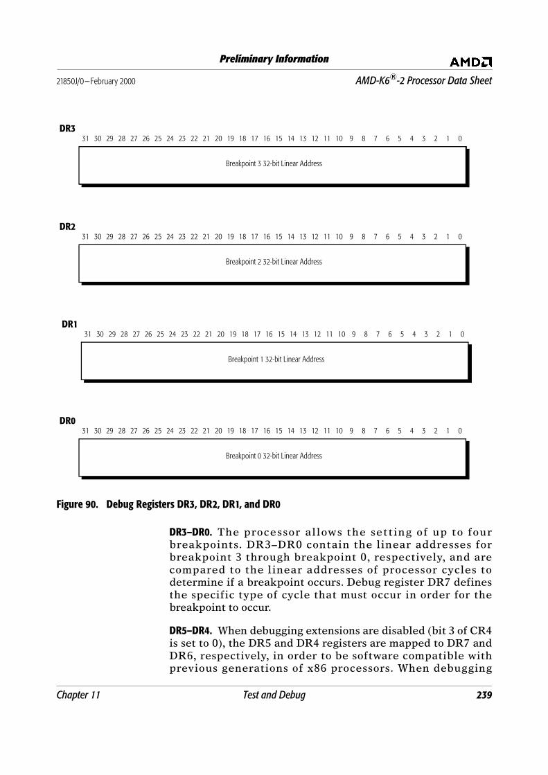
Chapter 11 Test and Debug 239
21850J/0—February 2000 AMD-K6®-2 Processor Data Sheet
Preliminary Information
Figure 90. Debug Registers DR3, DR2, DR1, and DR0
DR3–DR0. The processor allows the setting of up to four
breakpoints. DR3–DR0 contain the linear addresses for
breakpoint 3 through breakpoint 0, respectively, and are
compared to the linear addresses of processor cycles to
determine if a breakpoint occurs. Debug register DR7 defines
the specific type of cycle that must occur in order for the
breakpoint to occur.
DR5–DR4. When debugging extensions are disabled (bit 3 of CR4
is set to 0), the DR5 and DR4 registers are mapped to DR7 and
DR6, respectively, in order to be software compatible with
previous generations of x86 processors. When debugging
9 8 7 6 5 4 3 2 1 010111213141516171819202131 30 29 28 27 26 25 24 23 22
Breakpoint 3 32-bit Linear Address
DR3
9 8 7 6 5 4 3 2 1 010111213141516171819202131 30 29 28 27 26 25 24 23 22
Breakpoint 0 32-bit Linear Address
DR0
9 8 7 6 5 4 3 2 1 010111213141516171819202131 30 29 28 27 26 25 24 23 22
Breakpoint 2 32-bit Linear Address
DR2
9 8 7 6 5 4 3 2 1 010111213141516171819202131 30 29 28 27 26 25 24 23 22
Breakpoint 1 32-bit Linear Address
DR1

240 Test and Debug Chapter 11
AMD-K6®-2 Processor Data Sheet 21850J/0—February 2000
Preliminary Information
extensions are enabled (bit 3 of CR4 is set to 1), any attempt to
load DR5 or DR4 results in an undefined opcode exception.
Likewise, any attempt to store DR5 or DR4 also results in an
undefined opcode exception.
DR6. If a breakpoint is enabled in DR7, and the breakpoint
conditions as defined in DR7 occur, then the corresponding
B-bit (B3–B0) in DR6 is set to 1. In addition, any other
breakpoints defined using these particular breakpoint
conditions are reported by the processor by setting the
appropriate B-bits in DR6, regardless of whether these
breakpoints are enabled or disabled. However, if a breakpoint is
not enabled, a debug exception does not occur for that
breakpoint.
If the processor decodes an instruction that writes or reads DR7
through DR0, the BD bit (bit 13) in DR6 is set to 1 (if enabled in
DR7) and the processor generates a debug exception. This
operation allows control to pass to the debugger prior to debug
register access by software.
If the Trap Flag (bit 8) of the EFLAGS register is set to 1, the
processor generates a debug exception after the successful
execution of every instruction (single-step operation) and sets
the BS bit (bit 14) in DR6 to indicate the source of the
exception.
When the processor switches to a new task and the debug trap
bit (T-bit) in the corresponding Task State Segment (TSS) is set
to 1, the processor sets the BT bit (bit 15) in DR6 and generates
a debug exception.
DR7. When set to 1, L3–L0 locally enable breakpoints 3 through
0, respectively. L3–L0 are set to 0 whenever the processor
executes a task switch. Setting L3–L0 to 0 disables the
breakpoints and ensures that these particular debug exceptions
are only generated for a specific task.
When set to 1, G3–G0 globally enable breakpoints 3 through 0,
respectively. Unlike L3–L0, G3–G0 are not set to 0 whenever the
processor executes a task switch. Not setting G3–G0 to 0 allows
breakpoints to remain enabled across all tasks. If a breakpoint
is enabled globally but disabled locally, the global enable
overrides the local enable.

Chapter 11 Test and Debug 241
21850J/0—February 2000 AMD-K6®-2 Processor Data Sheet
Preliminary Information
The LE (bit 8) and GE (bit 9) bits in DR7 have no effect on the
operation of the processor and are provided in order to be
software compatible with previous generations of x86
processors.
When set to 1, the GD bit in DR7 (bit 13) enables the debug
exception associated with the BD bit (bit 13) in DR6. This bit is
set to 0 when a debug exception is generated.
LEN3–LEN0 and RW3–RW0 are two-bit fields in DR7 that
specify the length and type of each breakpoint as defined in
Table 51.
Debug Exceptions A debug exception is categorized as either a debug trap or a
debug fault. A debug trap calls the debugger following the
execution of the instruction that caused the trap. A debug fault
calls the debugger prior to the execution of the instruction that
caused the fault. All debug traps and faults generate either an
Interrupt 01h or an Interrupt 03h exception.
Table 51. DR7 LEN and RW Definitions
LEN Bits1 RW Bits Breakpoint
00b 00b2 Instruction Execution
00b
01b
One-byte Data Write
01b Two-byte Data Write
11b Four-byte Data Write
00b
10b3
One-byte I/O Read or Write
01b Two-byte I/O Read or Write
11b Four-byte I/O Read or Write
00b
11b
One-byte Data Read or Write
01b Two-byte Data Read or Write
11b Four-byte Data Read or Write
Notes:
1. LEN bits equal to 10b is undefined.
2. When RW equals 00b, LEN must be equal to 00b.
3. When RW equals 10b, debugging extensions (DE) must be enabled (bit 3 of CR4 must be setto 1). If DE is set to 0, then RW equal to 10b is undefined.

242 Test and Debug Chapter 11
AMD-K6®-2 Processor Data Sheet 21850J/0—February 2000
Preliminary Information
Interrupt 01h. The following events are considered debug traps
that cause the processor to generate an Interrupt 01h
exception:
Enabled breakpoints for data and I/O cycles
Single Step Trap
Task Switch Trap
The following events are considered debug faults that cause the
processor to generate an Interrupt 01h exception:
Enabled breakpoints for instruction execution
BD bit in DR6 set to 1
Interrupt 03h. The INT 3 instruction is defined in the x86
architecture as a breakpoint instruction. This instruction
causes the processor to generate an Interrupt 03h exception.
This exception is a debug trap because the debugger is called
following the execution of the INT 3 instruction.
The INT 3 instruction is a one-byte instruction (opcode CCh)
typically used to insert a breakpoint in software by writing CCh
to the address of the first byte of the instruction to be trapped
(the target instruction). Following the trap, if the target
instruction is to be executed, the debugger must replace the
INT 3 instruction with the first byte of the target instruction.

Chapter 12 Clock Control 243
21850J/0—February 2000 AMD-K6®-2 Processor Data Sheet
Preliminary Information
12 Clock Control
The AMD-K6-2 processor supports five modes of clock control.
The processor can transition between these modes to maximize
performance, to minimize power dissipation, or to provide a
balance between performance and power. (See “Power
Dissipation” on page 257 for the maximum power dissipation of
the AMD-K6-2 processor within the normal and reduced-power
states.)
The five clock-control states supported are as follows:
Normal State: The processor is running in Real Mode,
Virtual-8086 Mode, Protected Mode, or System Management
Mode (SMM). In this state, all clocks are running—including
the external bus clock CLK and the internal processor
clock—and the full features and functions of the processor
are available.
Halt State: This low-power state is entered following the
successful execution of the HLT instruction. During this
state, the internal processor clock is stopped.
Stop Grant State: This low-power state is entered following
the recognition of the assertion of the STPCLK# signal.
During this state, the internal processor clock is stopped.
Stop Grant Inquire State: This state is entered from the Halt
state and the Stop Grant state as the result of a
system-initiated inquire cycle.
Stop Clock State: This low-power state is entered from the
Stop Grant state when the CLK signal is stopped.
The following sections describe each of the four low-power
states. Figure 91 on page 248 illustrates the clock control state
transitions.
244 Clock Control Chapter 12
AMD-K6®-2 Processor Data Sheet 21850J/0—February 2000
Preliminary Information
12.1 Halt State
Enter Halt State During the execution of the HLT instruction, the AMD-K6-2
processor executes a Halt special cycle. After BRDY# is
sampled asserted during this cycle, and then EWBE# is also
sampled asserted (if not masked off), the processor enters the
Halt state in which the processor disables most of its internal
clock distribution. In order to support the following operations,
the internal phase-lock loop (PLL) still runs, and some internal
resources are still clocked in the Halt state:
Inquire Cycles: The processor continues to sample AHOLD,
BOFF#, and HOLD in order to support inquire cycles that
are initiated by the system logic. The processor transitions to
the Stop Grant Inquire state during the inquire cycle. After
returning to the Halt state following the inquire cycle, the
processor does not execute another Halt special cycle.
Flush Cycles: The processor continues to sample FLUSH#. If
FLUSH# is sampled asserted, the processor performs the
flush operation in the same manner as it is performed in the
Normal state. Upon completing the flush operation, the
processor executes the Halt special cycle which indicates
the processor is in the Halt state.
Time Stamp Counter (TSC): The TSC continues to count in
the Halt state.
Signal Sampling: The processor continues to sample INIT,
INTR, NMI, RESET, and SMI#.
After entering the Halt state, all signals driven by the processor
retain their state as they existed following the completion of
the Halt special cycle.
Exit Halt State The AMD-K6-2 processor remains in the Halt state until it
samples INIT, INTR (if interrupts are enabled), NMI, RESET, or
SMI# asserted. If any of these signals is sampled asserted, the
processor returns to the Normal state and performs the
corresponding operation. All of the normal requirements for
recognition of these input signals apply within the Halt state.

Chapter 12 Clock Control 245
21850J/0—February 2000 AMD-K6®-2 Processor Data Sheet
Preliminary Information
12.2 Stop Grant State
Enter Stop Grant State
After recognizing the assertion of STPCLK#, the AMD-K6-2
processor flushes its instruction pipelines, completes all
pending and in-progress bus cycles, and acknowledges the
STPCLK# assertion by executing a Stop Grant special bus cycle.
After BRDY# is sampled asserted during this cycle, and then
EWBE# is also sampled asserted (if not masked off), the
processor enters the Stop Grant state. The Stop Grant state is
like the Halt state in that the processor disables most of its
internal clock distribution in the Stop Grant state. In order to
support the following operations, the internal PLL still runs,
and some internal resources are still clocked in the Stop Grant
state:
Inquire cycles: The processor transitions to the Stop Grant
Inquire state during an inquire cycle. After returning to the
Stop Grant state following the inquire cycle, the processor
does not execute another Stop Grant special cycle.
Time Stamp Counter (TSC): The TSC continues to count in
the Stop Grant state.
Signal Sampling: The processor continues to sample INIT,
INTR, NMI, RESET, and SMI#.
FLUSH# is not recognized in the Stop Grant state (unlike while
in the Halt state).
Upon entering the Stop Grant state, all signals driven by the
processor retain their state as they existed following the
completion of the Stop Grant special cycle.
Exit Stop Grant State The AMD-K6-2 processor remains in the Stop Grant state until
it samples STPCLK# negated or RESET asserted. If STPCLK#
is sampled negated, the processor returns to the Normal state in
less than 10 bus clock (CLK) periods. After the transition to the
Normal state, the processor resumes execution at the
instruction boundary on which STPCLK# was initially
recognized.
If STPCLK# is recognized as negated in the Stop Grant state
and subsequently sampled asserted prior to returning to the
Normal state, the AMD-K6-2 processor guarantees that a
minimum of one instruction is executed prior to re-entering the
Stop Grant state.

246 Clock Control Chapter 12
AMD-K6®-2 Processor Data Sheet 21850J/0—February 2000
Preliminary Information
If INIT, INTR (if interrupts are enabled), FLUSH#, NMI, or
SMI# are sampled asserted in the Stop Grant state, the
processor latches the edge-sensitive signals (INIT, FLUSH#,
NMI, and SMI#), but otherwise does not exit the Stop Grant
state to service the interrupt. When the processor returns to the
Normal state due to sampling STPCLK# negated, any pending
interrupts are recognized after returning to the Normal state.
To ensure their recognition, all of the normal requirements for
these input signals apply within the Stop Grant state.
If RESET is sampled asserted in the Stop Grant state, the
processor immediately returns to the Normal state and the
reset process begins.
12.3 Stop Grant Inquire State
Enter Stop Grant Inquire State
The Stop Grant Inquire state is entered from the Stop Grant
state or the Halt state when EADS# is sampled asserted during
an inquire cycle initiated by the system logic. The AMD-K6-2
processor responds to an inquire cycle in the same manner as in
the Normal state by driving HIT# and HITM#. If the inquire
cycle hits a modified data cache line, the processor performs a
writeback cycle.
Exit Stop Grant Inquire State
Following the completion of any writeback, the processor
returns to the state from which it entered the Stop Grant
Inquire state.
12.4 Stop Clock State
Enter Stop Clock State
If the CLK signal is stopped while the AMD-K6-2 processor is in
the Stop Grant state, the processor enters the Stop Clock state.
Because all internal clocks and the PLL are not running in the
Stop Clock state, the Stop Clock state represents the
minimum-power state of all clock control states. The CLK signal
must be held Low while it is stopped.
The Stop Clock state cannot be entered from the Halt state.
INTR is the only input signal that is allowed to change states
while the processor is in the Stop Clock state. However, INTR is
not sampled until the processor returns to the Stop Grant state.
All other input signals must remain unchanged in the Stop
Clock state.

Chapter 12 Clock Control 247
21850J/0—February 2000 AMD-K6®-2 Processor Data Sheet
Preliminary Information
Exit Stop Clock State The AMD-K6-2 processor returns to the Stop Grant state from
the Stop Clock state after the CLK signal is started and the
internal PLL has stabilized. PLL stabilization is achieved after
the CLK signal has been running within its specification for a
minimum of 1.0 ms.
The frequency of CLK when exiting the Stop Clock state can be
different than the frequency of CLK when entering the Stop
Clock state.
The state of the BF[2:0] signals when exiting the Stop Clock
state is ignored because the BF[2:0] signals are only sampled
during the falling transition of RESET.

248 Clock Control Chapter 12
AMD-K6®-2 Processor Data Sheet 21850J/0—February 2000
Preliminary Information
Figure 91. Clock Control State Transitions
EADS# Asserted EADS# Asserted
HLT Instruction
Stop GrantState
Normal Mode - Real
- Virtual-8086
- Protected - SMM
HaltState
Stop ClockState
RESET, SMI#, INIT,
or INTR Asserted
Stop GrantInquireState
STPCLK# Asserted
STPCLK# Negated,
or RESET Asserted
CLK
Started
CLK
Stopped
WritebackCompleted
WritebackCompleted
Chapter 13 Power and Grounding 249
21850J/0—February 2000 AMD-K6®-2 Processor Data Sheet
Preliminary Information
13 Power and Grounding
13.1 Power Connections
The AMD-K6-2 processor is a dual voltage device. Two separate
supply voltages are required: VCC2 and VCC3. VCC2 provides the
core voltage for the processor and VCC3 provides the I/O voltage.
See “Electrical Data” on page 253 for the value and range of
VCC2 and VCC3.
There are 28 VCC2, 32 VCC3, and 68 VSS pins on the AMD-K6-2
processor. (See “Pin Designations” on page 297 for all power
and ground pin designations.) The large number of power and
ground pins are provided to ensure that the processor and
package maintain a clean and stable power distribution
network.
For proper operation and functionality, all VCC2, VCC3, and VSSpins must be connected to the appropriate planes in the circuit
board. The power planes have been arranged in a pattern to
simplify routing and minimize crosstalk on the circuit board.
The isolation region between two voltage planes must be at
least 0.254mm if they are in the same layer of the circuit board.
(See Figure 92 on page 250.) In order to maintain a
low-impedance current sink and reference, the ground plane
must never be split.
Although the AMD-K6-2 processor has two separate supply
voltages, there are no special power sequencing requirements.
The best procedure is to minimize the time between which VCC2and VCC3 are either both on or both off.

250 Power and Grounding Chapter 13
AMD-K6®-2 Processor Data Sheet 21850J/0—February 2000
Preliminary Information
Figure 92. Suggested Component Placement
13.2 Decoupling Recommendations
In addition to the isolation region mentioned in “Power
Connections” on page 249, adequate decoupling capacitance is
required between the two system power planes and the ground
plane to minimize ringing and to provide a low-impedance path
for return currents. Suggested decoupling capacitor placement
is shown in Figure 92.
Surface mounted capacitors should be used under the
processor’s ZIF socket to minimize resistance and inductance in
the lead lengths while maintaining minimal height. For
information and recommendations about the specific value,
quantity, and location of the capacitors, see the AMD-K6®
Processor Power Supply Design Application Note, order# 21103.
0.254mm (min.) for isolation region
VCC2 (Core) PlaneVCC3 (I/O) Plane
C1
CC5
CC3
C2
+
++
+
C5
C6
C7
C11
C12
C13
C17C18
C19
C20
C21
C22
C23
C24
C25
C26
C27
C28
C29
C30
C31
CC4
+
CC6
CC
10
CC1 CC2
CC
9C
C8
CC
7
C8
C9
C10
C14
C15
C16

Chapter 13 Power and Grounding 251
21850J/0—February 2000 AMD-K6®-2 Processor Data Sheet
Preliminary Information
13.3 Pin Connection Requirements
For proper operation, the following requirements for signal pin
connections must be met:
Do not drive address and data signals into large capacitive
loads at high frequencies. If necessary, use buffer chips to
drive large capacitive loads.
Leave all NC (no-connect) pins unconnected.
Unused inputs should always be connected to an
appropriate signal level.
• Active Low inputs that are not being used should be
connected to VCC3 through a 20-kohm pullup resistor.
• Active High inputs that are not being used should be
connected to GND through a pulldown resistor.
Reserved signals can be treated in one of the following ways:
• As no-connect (NC) pins, in which case these pins are left
unconnected
• As pins connected to the system logic as defined by the
industry-standard Super7 and Socket 7 interface
• Any combination of NC and Socket 7 pins
Keep trace lengths to a minimum.

252 Power and Grounding Chapter 13
AMD-K6®-2 Processor Data Sheet 21850J/0—February 2000
Preliminary Information

Chapter 14 Electrical Data 253
21850J/0—February 2000 AMD-K6®-2 Processor Data Sheet
Preliminary Information
14 Electrical Data
This chapter consists of two sections, where each section
provides the electrical specifications of the AMD-K6-2
processor based on specific Ordering Part Number (OPN)
suffixes. See “Ordering Information” on page 301 for a
complete list and description of the valid OPN combinations.
14.1 Electrical Data for OPN Suffixes AHX, 400AFQ, and AFR
The electrical specifications provided in this section pertain to
the following OPNs:
Note: The electrical specifications for the AMD-K6-2/400AFR OPN
are provided in “Electrical Data for OPN Suffixes AGR,
AFX, and 400AFR” on page 258.
Operating Ranges The AMD-K6-2 processor is designed to provide functional
operation if the voltage and temperature parameters are within
the limits defined in Table 52.
AMD-K6-2/475AHX AMD-K6-2/450AHX AMD-K6-2/400AFQ
AMD-K6-2/380AFR AMD-K6-2/366AFR AMD-K6-2/350AFR
AMD-K6-2/333AFR AMD-K6-2/300AFR AMD-K6-2/266AFR
Table 52. Operating Ranges for OPN Suffixes AHX, 400AFQ, and AFR
Parameter Minimum Typical Maximum Comments
VCC22.1 V 2.2 V 2.3 V Note 1, 2
2.3 V 2.4 V 2.5 V Note 1, 3
VCC3 3.135 V 3.30 V 3.6 V Note 1
TCASE 0°C
70°C Note 4
65°C Note 5
60°C Note 6
Notes:
1. VCC2 and VCC3 are referenced from VSS.
2. VCC2 specification for 2.2 V component.
3. VCC2 specification for 2.4 V component.
4. Case temperature range required for AMD-K6-2/xxxAFR valid ordering part numbercombinations, where “xxx” represents the processor core frequency.
5. Case temperature range required for AMD-K6-2/xxxAHX valid ordering part numbercombinations, where “xxx” represents the processor core frequency.
6. Case temperature range required for AMD-K6-2/xxxAFQ valid ordering part numbercombinations, where “xxx” represents the processor core frequency.

254 Electrical Data Chapter 14
AMD-K6®-2 Processor Data Sheet 21850J/0—February 2000
Preliminary Information
Absolute Ratings The AMD-K6-2 processor is not designed to be operated beyond
the operating ranges listed in Table 52. Exposure to conditions
outside these operating ranges for extended periods of time can
affect long-term reliability. Permanent damage can occur if the
absolute ratings listed in Table 53 are exceeded.
DC Characteristics The DC characteristics of the AMD-K6-2 processor are shown in
Table 54.
Table 53. Absolute Ratings for OPN Suffixes AHX, 400AFQ, and AFR
Parameter Minimum Maximum Comments
VCC2 –0.5 V 2.6 V
VCC3 –0.5 V 3.6 V
VPIN –0.5 VVCC3 + 0.5 V and
≤ 4.0 VNote
TCASE (under bias) –65°C +110°C
TSTORAGE –65°C +150°C
Note:
VPIN (the voltage on any I/O pin) must not be greater than 0.5 V above the voltage beingapplied to VCC3. In addition, the VPIN voltage must never exceed 4.0 V.
Table 54. DC Characteristics for OPN Suffixes AHX, 400AFQ, and AFR
Symbol Parameter DescriptionPreliminary Data
CommentsMin Max
VIL Input Low Voltage –0.3 V +0.8 V
VIH Input High Voltage 2.0 V VCC3+0.3V Note 1
VOL Output Low Voltage 0.4 V IOL = 4.0-mA load
VOH Output High Voltage 2.4 V IOH = 3.0-mA load
Notes:
1. VCC3 refers to the voltage being applied to VCC3 during functional operation.
2. VCC2 = 2.3 V — The maximum power supply current must be taken into account when designing a power supply.
3. VCC2 = 2.5 V — The maximum power supply current must be taken into account when designing a power supply.
4. VCC3 = 3.6 V — The maximum power supply current must be taken into account when designing a power supply.
5. Refers to inputs and I/O without an internal pullup resistor and 0 ≤ VIN ≤ VCC3.
6. Refers to inputs with an internal pullup and VIL = 0.4 V.
7. Refers to inputs with an internal pulldown and VIH = 2.4 V.
8. This specification applies to components using a CLK frequency of 66 MHz.
9. This specification applies to components using a CLK frequency of 95 MHz.
10. This specification applies to components using a CLK frequency of 100 MHz.

Chapter 14 Electrical Data 255
21850J/0—February 2000 AMD-K6®-2 Processor Data Sheet
Preliminary Information
ICC2
2.2 V Power Supply Current
7.35 A 266 MHz, Note 2, 8
8.45 A 300 MHz, Note 2, 8, 10
9.40 A 333 MHz, Note 2, 8, 9
9.85 A 350 MHz, Note 2, 10
10.30 A 366 MHz, Note 2, 8
10.70 A 380 MHz, Note 2, 9
11.25 A 400 MHz, Note 2, 8, 10
2.4 V Power Supply Current12.50 A 450 MHz, Note 3, 10
13.00 A 475 MHz, Note 3, 9
ICC3 3.3 V Power Supply Current
0.54 A 266 MHz, Note 4, 8
0.56 A 300 MHz, Note 4, 8, 10
0.58 A 333 MHz, Note 4 , 8, 9
0.60 A 350 MHz, Note 4, 10
0.60 A 366 MHz, Note 4, 8
0.61 A 380 MHz, Note 4, 9
0.62 A 400 MHz, Note 4, 8, 10
0.66 A 450 MHz, Note 4, 10
0.67 A 475 MHz, Note 4, 9
ILI Input Leakage Current ±15 µA Note 5
ILO Output Leakage Current ±15 µA Note 5
IIL Input Leakage Current Bias with Pullup –400 µA Note 6
IIH Input Leakage Current Bias with Pulldown 200 µA Note 7
CIN Input Capacitance 10 pF
COUT Output Capacitance 15 pF
Table 54. DC Characteristics for OPN Suffixes AHX, 400AFQ, and AFR (continued)
Symbol Parameter DescriptionPreliminary Data
CommentsMin Max
Notes:
1. VCC3 refers to the voltage being applied to VCC3 during functional operation.
2. VCC2 = 2.3 V — The maximum power supply current must be taken into account when designing a power supply.
3. VCC2 = 2.5 V — The maximum power supply current must be taken into account when designing a power supply.
4. VCC3 = 3.6 V — The maximum power supply current must be taken into account when designing a power supply.
5. Refers to inputs and I/O without an internal pullup resistor and 0 ≤ VIN ≤ VCC3.
6. Refers to inputs with an internal pullup and VIL = 0.4 V.
7. Refers to inputs with an internal pulldown and VIH = 2.4 V.
8. This specification applies to components using a CLK frequency of 66 MHz.
9. This specification applies to components using a CLK frequency of 95 MHz.
10. This specification applies to components using a CLK frequency of 100 MHz.

256 Electrical Data Chapter 14
AMD-K6®-2 Processor Data Sheet 21850J/0—February 2000
Preliminary Information
COUT I/O Capacitance 20 pF
CCLK CLK Capacitance 10 pF
CTIN Test Input Capacitance (TDI, TMS, TRST#) 10 pF
CTOUT Test Output Capacitance (TDO) 15 pF
CTCK TCK Capacitance 10 pF
Table 54. DC Characteristics for OPN Suffixes AHX, 400AFQ, and AFR (continued)
Symbol Parameter DescriptionPreliminary Data
CommentsMin Max
Notes:
1. VCC3 refers to the voltage being applied to VCC3 during functional operation.
2. VCC2 = 2.3 V — The maximum power supply current must be taken into account when designing a power supply.
3. VCC2 = 2.5 V — The maximum power supply current must be taken into account when designing a power supply.
4. VCC3 = 3.6 V — The maximum power supply current must be taken into account when designing a power supply.
5. Refers to inputs and I/O without an internal pullup resistor and 0 ≤ VIN ≤ VCC3.
6. Refers to inputs with an internal pullup and VIL = 0.4 V.
7. Refers to inputs with an internal pulldown and VIH = 2.4 V.
8. This specification applies to components using a CLK frequency of 66 MHz.
9. This specification applies to components using a CLK frequency of 95 MHz.
10. This specification applies to components using a CLK frequency of 100 MHz.

Chapter 14 Electrical Data 257
21850J/0—February 2000 AMD-K6®-2 Processor Data Sheet
Preliminary Information
Power Dissipation Table 55 contains the typical and maximum power dissipation
of the AMD-K6-2 processor during normal and reduced power
states.
Table 55. Typical and Maximum Power Dissipation for OPN Suffixes AHX, 400AFQ, and AFR
Clock Control State
266
MHz6
300
MHz6,8
333
MHz6,7
350
MHz8
366
MHz6
380
MHz7
400
MHz6,8
450
MHz8
475
MHz7 Notes
Thermal Power(Maximum)
14.70 W 17.20 W 19.00 W 19.95 W 20.80 W 21.60 W 22.70 W 28.40 W 29.60 W 1, 2
Thermal Power(Typical)
8.85 W 10.35 W 11.40 W 11.98 W 12.48 W 12.95 W 13.65 W 17.05 W 17.75 W 3
Stop Grant / Halt (Maximum)
3.90 W 3.92 W 3.94 W 3.96 W 3.96 W 3.97 W 3.98 W 6.50 W 6.51 W 4
Stop Clock (Maximum)
3.50 W 3.50 W 3.50 W 3.50 W 3.50 W 3.50 W 3.50 W 6.00 W 6.00 W 5
Notes:
1. The maximum power dissipated in the normal clock control state must be taken into account when designing a solution for thermaldissipation for the AMD-K6-2 processor.
2. Maximum power is determined for the worst-case instruction sequence or function for the listed clock control states with VCC2 = 2.2 V (for the 2.2 V component) or VCC2 = 2.4 V (for the 2.4 V component) and VCC3 = 3.3 V.
3. Typical power is determined for the typical instruction sequences or functions associated with normal system operation with VCC2 = 2.2 V (for the 2.2 V component) or VCC2 = 2.4 V (for the 2.4 V component) and VCC3 = 3.3 V.
4. The CLK signal and the internal PLL are still running but most internal clocking has stopped.
5. The CLK signal, the internal PLL, and all internal clocking has stopped.
6. This specification applies to components using a CLK frequency of 66 MHz.
7. This specification applies to components using a CLK frequency of 95 MHz.
8. This specification applies to components using a CLK frequency of 100 MHz.

258 Electrical Data Chapter 14
AMD-K6®-2 Processor Data Sheet 21850J/0—February 2000
Preliminary Information
14.2 Electrical Data for OPN Suffixes AGR, AFX, and 400AFR
The electrical specifications provided in this section pertain to
the following OPNs:
Note: The electrical specifications for all frequencies of the OPN
suffix AFR other than 400 MHz are provided in “Electrical
Data for OPN Suffixes AHX, 400AFQ, and AFR” on
page 253.
Operating Ranges The AMD-K6-2 processor is designed to provide functional
operation if the voltage and temperature parameters are within
the limits defined in Table 56.
AMD-K6-2/550AGR AMD-K6-2/533AFX AMD-K6-2/500AFX
AMD-K6-2/475AFX AMD-K6-2/450AFX AMD-K6-2/400AFR
Table 56. Operating Ranges for OPN Suffixes AGR, AFX, and 400AFR
Parameter Minimum Typical Maximum Comments
VCC2 2.1 V 2.2 V 2.3 V Note 1, 2
VCC2 2.2 V 2.3 V 2.4 V Note 1, 3
VCC3 3.135 V 3.30 V 3.6 V Note 1
TCASE 0°C 70°C Note 4
TCASE 0°C 65°C Note 5
Notes:
1. VCC2 and VCC3 are referenced from VSS.
2. VCC2 specification for 2.2 V components.
3. VCC2 specification for 2.3 V components.
4. Case temperature range required for AMD-K6-2/550AGR and AMD-K6-2/400AFR orderingpart numbers.
5. Case temperature range required for AMD-K6-2/xxxAHX valid ordering part numbercombinations, where “xxx” represents the processor core frequency.

Chapter 14 Electrical Data 259
21850J/0—February 2000 AMD-K6®-2 Processor Data Sheet
Preliminary Information
Absolute Ratings The AMD-K6-2 processor is not designed to be operated beyond
the operating ranges listed in Table 56. Exposure to conditions
outside these operating ranges for extended periods of time can
affect long-term reliability. Permanent damage can occur if the
absolute ratings listed in Table 57 are exceeded.
DC Characteristics The DC characteristics of the AMD-K6-2 processor are shown in
Table 58.
Table 57. Absolute Ratings for OPN Suffixes AGR, AFX, and 400AFR
Parameter Minimum Maximum Comments
VCC2 –0.5 V 2.5 V
VCC3 –0.5 V 3.6 V
VPIN –0.5 VVCC3 + 0.5 V and
≤ 4.0 VNote
TCASE (under bias) –65°C +110°C
TSTORAGE –65°C +150°C
Note:
VPIN (the voltage on any I/O pin) must not be greater than 0.5 V above the voltage beingapplied to VCC3. In addition, the VPIN voltage must never exceed 4.0 V.
Table 58. DC Characteristics for OPN Suffixes AGR, AFX, and 400AFR
Symbol Parameter DescriptionPreliminary Data
CommentsMin Max
VIL Input Low Voltage –0.3 V +0.8 V
VIH Input High Voltage 2.0 V VCC3+0.3V Note 1
VOL Output Low Voltage 0.4 V IOL = 4.0-mA load
VOH Output High Voltage 2.4 V IOH = 3.0-mA load
Notes:
1. VCC3 refers to the voltage being applied to VCC3 during functional operation.
2. VCC2 = 2.3 V — The maximum power supply current must be taken into account when designing a power supply.
3. VCC2 = 2.4 V — The maximum power supply current must be taken into account when designing a power supply.
4. VCC3 = 3.6 V — The maximum power supply current must be taken into account when designing a power supply.
5. Refers to inputs and I/O without an internal pullup resistor and 0 ≤ VIN ≤ VCC3.
6. Refers to inputs with an internal pullup and VIL = 0.4 V.
7. Refers to inputs with an internal pulldown and VIH = 2.4 V.
8. This specification applies to components using a CLK frequency of 66 MHz.
9. This specification applies to components using a CLK frequency of 95 MHz.
10. This specification applies to components using a CLK frequency of 100 MHz.
11. This specification applies to components using a CLK frequency of 97 MHz.
12. The specifications provided for the 533 MHz component are identical to the specifications of the 500 MHz component.

260 Electrical Data Chapter 14
AMD-K6®-2 Processor Data Sheet 21850J/0—February 2000
Preliminary Information
ICC2 2.2 V Power Supply Current
10.00 A 400 MHz, Note 2, 8, 10
11.25 A 450 MHz, Note 2, 10
11.90 A 475 MHz, Note 2, 9
12.50 A500 MHz, Note 2, 10
533 MHz, Note 2, 11, 12
2.3 V Power Supply Current 13.00 A 550 MHz, Note 3, 10
ICC3 3.3 V Power Supply Current
0.62 A 400 MHz, Note 4, 8, 10
0.66 A 450 MHz, Note 4, 10
0.67 A 475 MHz, Note 4, 9
0.69 A
500 MHz, Note 4, 10
533 MHz, Note 4, 11, 12
550 MHz, Note 4, 10
ILI Input Leakage Current ±15 µA Note 5
ILO Output Leakage Current ±15 µA Note 5
IIL Input Leakage Current Bias with Pullup –400 µA Note 6
IIH Input Leakage Current Bias with Pulldown 200 µA Note 7
CIN Input Capacitance 10 pF
COUT Output Capacitance 15 pF
COUT I/O Capacitance 20 pF
CCLK CLK Capacitance 10 pF
CTIN Test Input Capacitance (TDI, TMS, TRST#) 10 pF
CTOUT Test Output Capacitance (TDO) 15 pF
Table 58. DC Characteristics for OPN Suffixes AGR, AFX, and 400AFR (continued)
Symbol Parameter DescriptionPreliminary Data
CommentsMin Max
Notes:
1. VCC3 refers to the voltage being applied to VCC3 during functional operation.
2. VCC2 = 2.3 V — The maximum power supply current must be taken into account when designing a power supply.
3. VCC2 = 2.4 V — The maximum power supply current must be taken into account when designing a power supply.
4. VCC3 = 3.6 V — The maximum power supply current must be taken into account when designing a power supply.
5. Refers to inputs and I/O without an internal pullup resistor and 0 ≤ VIN ≤ VCC3.
6. Refers to inputs with an internal pullup and VIL = 0.4 V.
7. Refers to inputs with an internal pulldown and VIH = 2.4 V.
8. This specification applies to components using a CLK frequency of 66 MHz.
9. This specification applies to components using a CLK frequency of 95 MHz.
10. This specification applies to components using a CLK frequency of 100 MHz.
11. This specification applies to components using a CLK frequency of 97 MHz.
12. The specifications provided for the 533 MHz component are identical to the specifications of the 500 MHz component.

Chapter 14 Electrical Data 261
21850J/0—February 2000 AMD-K6®-2 Processor Data Sheet
Preliminary Information
CTCK TCK Capacitance 10 pF
Table 58. DC Characteristics for OPN Suffixes AGR, AFX, and 400AFR (continued)
Symbol Parameter DescriptionPreliminary Data
CommentsMin Max
Notes:
1. VCC3 refers to the voltage being applied to VCC3 during functional operation.
2. VCC2 = 2.3 V — The maximum power supply current must be taken into account when designing a power supply.
3. VCC2 = 2.4 V — The maximum power supply current must be taken into account when designing a power supply.
4. VCC3 = 3.6 V — The maximum power supply current must be taken into account when designing a power supply.
5. Refers to inputs and I/O without an internal pullup resistor and 0 ≤ VIN ≤ VCC3.
6. Refers to inputs with an internal pullup and VIL = 0.4 V.
7. Refers to inputs with an internal pulldown and VIH = 2.4 V.
8. This specification applies to components using a CLK frequency of 66 MHz.
9. This specification applies to components using a CLK frequency of 95 MHz.
10. This specification applies to components using a CLK frequency of 100 MHz.
11. This specification applies to components using a CLK frequency of 97 MHz.
12. The specifications provided for the 533 MHz component are identical to the specifications of the 500 MHz component.

262 Electrical Data Chapter 14
AMD-K6®-2 Processor Data Sheet 21850J/0—February 2000
Preliminary Information
Power Dissipation Table 59 contains the typical and maximum power dissipation
of the AMD-K6-2 processor during normal and reduced power
states.
Table 59. Typical and Maximum Power Dissipation for OPN Suffixes AGR, AFX, and 400AFR
Clock Control State
400
MHz6,8
450
MHz8
475
MHz7
500
MHz8
533
MHz9,10
550
MHz8 Notes
Thermal Power(Maximum)
16.90 W 18.80 W 19.80 W 20.75 W 25.00 W 1, 2
Thermal Power(Typical)
10.15 W 11.30 W 11.90 W 12.45 W 15.00 W 3
Stop Grant / Halt (Maximum)
4.40 W 4.44 W 4.45 W 4.46 W 4.87 W 4
Stop Clock (Maximum)
4.00 W 4.00 W 4.00 W 4.00 W 4.37 W 5
Notes:
1. The maximum power dissipated in the normal clock control state must be taken into account whendesigning a solution for thermal dissipation for the AMD-K6-2 processor.
2. Maximum power is determined for the worst-case instruction sequence or function for the listedclock control states with VCC2 = 2.2 V (for 2.2 V components) or VCC2 = 2.3 V (for 2.3 V components)and VCC3 = 3.3 V.
3. Typical power is determined for the typical instruction sequences or functions associated withnormal system operation with VCC2 = 2.2 V (for 2.2 V components) or VCC2 = 2.3 V (for 2.3 Vcomponents) and VCC3 = 3.3 V.
4. The CLK signal and the internal PLL are still running but most internal clocking has stopped.
5. The CLK signal, the internal PLL, and all internal clocking has stopped.
6. This specification applies to components using a CLK frequency of 66 MHz.
7. This specification applies to components using a CLK frequency of 95 MHz.
8. This specification applies to components using a CLK frequency of 100 MHz.
9. This specification applies to components using a CLK frequency of 97 MHz.
10. The specifications provided for the 533 MHz component are identical to the specifications of the 500MHz component.
Chapter 15 I/O Buffer Characteristics 263
21850J/0—February 2000 AMD-K6®-2 Processor Data Sheet
Preliminary Information
15 I/O Buffer Characteristics
All of the AMD-K6-2 processor inputs , outputs , and
bidirectional buffers are implemented using a 3.3V buffer
design. In addition, a subset of the processor I/O buffers include
a second, higher drive strength option. These buffers can be
configured to provide the higher drive strength for applications
that place a heavier load on these I/O signals.
AMD has developed two I/O buffer models that represent the
characteristics of each of the two possible drive strength
configurations supported by the AMD-K6-2 processor. These
two models are called the Standard I/O Model and the Strong
I/O Model.
AMD developed the two models to allow system designers to
perform analog simulations of AMD-K6-2 processor signals that
interface with the system logic. Analog simulations are used to
determine a signal’s time of flight from source to destination
and to ensure that the system’s signal quality requirements are
met. Signal quality measurements include overshoot,
undershoot, slope reversal, and ringing.
15.1 Selectable Drive Strength
The AMD-K6-2 processor samples the BRDYC# input during the
falling transition of RESET to configure the drive strength of
A[20:3], ADS#, HITM# and W/R#. If BRDYC# is 0 during the fall
of RESET, these particular outputs are configured using the
higher drive strength. If BRDYC# is 1 during the fall of RESET,
the standard drive strength is selected for all I/O buffers.
Table 60 shows the relationship between BRDYC# and the two
available drive strengths — K6STD and K6STG.
Table 60. A[20:3], ADS#, HITM#, and W/R# Strength Selection
Drive Strength BRDYC# I/O Buffer Name
Strength 1 (standard) 1 K6STD
Strength 2 (strong) 0 K6STG
264 I/O Buffer Characteristics Chapter 15
AMD-K6®-2 Processor Data Sheet 21850J/0—February 2000
Preliminary Information
15.2 I/O Buffer Model
AMD provides models of the AMD-K6-2 processor I/O buffers
for system designers to use in board-level simulations. These I/O
buffer models conform to the I /O Buffer Information
Specification (IBIS). The Standard I/O Model uses K6STD, the
standard I/O buffer representation, for all I/O buffers. The
Strong I/O Model uses K6STG, the stronger I/O buffer
representation for A[20:3], ADS#, HITM#, and W/R#, and uses
K6STD for the remainder of the I/O buffers.
Both I/O models contain voltage versus current (V/I) and
voltage versus time (V/T) data tables for accurate modeling of
I/O buffer behavior.
The following list characterizes the properties of each I/O
buffer model:
All data tables contain minimum, typical, and maximum
values to allow for worst-case, typical, and best-case
simulations, respectively.
The pullup, pulldown, power clamp, and ground clamp
device V/I tables contain enough data points to accurately
represent the nonlinear nature of the V/I curves. In addition,
the voltage ranges provided in these tables extend beyond
the normal operating range of the AMD-K6-2 processor for
those simulators that yield more accurate results based on
this wider range. Figure 93 and Figure 94 on page 265
illustrate the min/typ/max pulldown and pullup V/I curves
for K6STD between 0V and 3.3V.
The rising and falling ramp rates are specified.
The min/typ/max VCC3 operating range is specified as
3.135V, 3.3V, and 3.6V, respectively.
Vil = 0.8V, Vih = 2.0V, and Vmeas = 1.5V
The R/L/C of the package is modeled.
The capacitance of the silicon die is modeled.
The model assumes a test load resistance of 50Ω.

Chapter 15 I/O Buffer Characteristics 265
21850J/0—February 2000 AMD-K6®-2 Processor Data Sheet
Preliminary Information
Figure 93. K6STD Pulldown V/I Curves
Figure 94. K6STD Pullup V/I Curves
15.3 I/O Model Application Note
For the AMD-K6-2 processor I/O Buffer IBIS Models and their
application, refer to the AMD-K6® Processor I/O Model (IBIS)
Application Note, order# 21084.
15.4 I/O Buffer AC and DC Characteristics
See “Signal Switching Characteristics” on page 267 for the
AMD-K6-2 processor AC timing specifications.
See “Electrical Data” on page 253 for the AMD-K6-2 processor
DC specifications.
0
10
20
30
40
50
60
70
0
0.3
0.6
0.9
1.2
1.5
1.8
2.1
2.4
2.7
3.0
3.3
Voutput (V)
I ol (
mA
)
-70
-60
-50
-40
-30
-20
-10
0
0 0.3
0.6
0.9
1.2
1.5
1.8
2.1
2.4
2.7
3.0
3.3
Voutput (V)
I oh
(mA
)

266 I/O Buffer Characteristics Chapter 15
AMD-K6®-2 Processor Data Sheet 21850J/0—February 2000
Preliminary Information

Chapter 16 Signal Switching Characteristics 267
21850J/0—February 2000 AMD-K6®-2 Processor Data Sheet
Preliminary Information
16 Signal Switching Characteristics
The AMD-K6-2 processor signal switching characteristics are
presented in Table 61 through Table 70. Valid delay, float,
setup, and hold timing specifications are listed. These
specifications are provided for the system designer to
determine if the timings necessary for the processor to
interface with the system logic are met. Table 61 and Table 62
contain the switching characteristics of the CLK input. Table 63
through Table 66 contain the timings for the normal operation
signals. Table 67 and Table 68 contain the timings for RESET
and the configuration signals. Table 69 and Table 70 contain the
timings for the test operation signals.
All signal timings provided are:
Measured between CLK, TCK, or RESET at 1.5 V and the
corresponding signal at 1.5 V—this applies to input and
output signals that are switching from Low to High, or from
High to Low
Based on input signals applied at a slew rate of 1 V/ns
between 0 V and 3 V (rising) and 3 V to 0 V (falling)
Valid within the operating ranges given in “Operating
Ranges” on page 253
Based on a load capacitance (CL) of 0 pF
16.1 CLK Switching Characteristics
Table 61 and Table 62 contain the switching characteristics of
the CLK input to the AMD-K6-2 processor for 100-MHz and
66-MHz bus operation, respectively, as measured at the voltage
levels indicated by Figure 95 on page 269.
The CLK Period Stability specifies the variance (jitter) allowed
between successive periods of the CLK input measured at 1.5 V.
This parameter must be considered as one of the elements of
clock skew between the AMD-K6-2 processor and the system
logic.
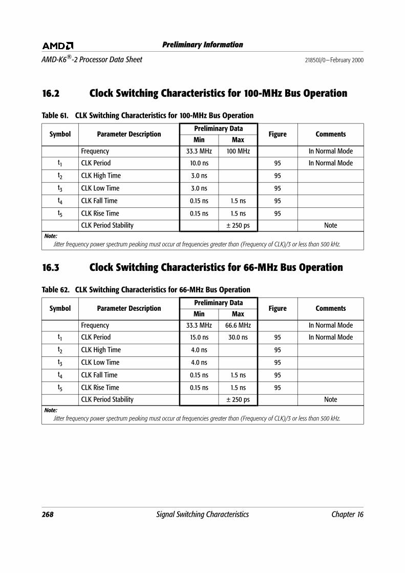
268 Signal Switching Characteristics Chapter 16
AMD-K6®-2 Processor Data Sheet 21850J/0—February 2000
Preliminary Information
16.2 Clock Switching Characteristics for 100-MHz Bus Operation
16.3 Clock Switching Characteristics for 66-MHz Bus Operation
Table 61. CLK Switching Characteristics for 100-MHz Bus Operation
Symbol Parameter DescriptionPreliminary Data
Figure CommentsMin Max
Frequency 33.3 MHz 100 MHz In Normal Mode
t1 CLK Period 10.0 ns 95 In Normal Mode
t2 CLK High Time 3.0 ns 95
t3 CLK Low Time 3.0 ns 95
t4 CLK Fall Time 0.15 ns 1.5 ns 95
t5 CLK Rise Time 0.15 ns 1.5 ns 95
CLK Period Stability ± 250 ps Note
Note:
Jitter frequency power spectrum peaking must occur at frequencies greater than (Frequency of CLK)/3 or less than 500 kHz.
Table 62. CLK Switching Characteristics for 66-MHz Bus Operation
Symbol Parameter DescriptionPreliminary Data
Figure CommentsMin Max
Frequency 33.3 MHz 66.6 MHz In Normal Mode
t1 CLK Period 15.0 ns 30.0 ns 95 In Normal Mode
t2 CLK High Time 4.0 ns 95
t3 CLK Low Time 4.0 ns 95
t4 CLK Fall Time 0.15 ns 1.5 ns 95
t5 CLK Rise Time 0.15 ns 1.5 ns 95
CLK Period Stability ± 250 ps Note
Note:
Jitter frequency power spectrum peaking must occur at frequencies greater than (Frequency of CLK)/3 or less than 500 kHz.

Chapter 16 Signal Switching Characteristics 269
21850J/0—February 2000 AMD-K6®-2 Processor Data Sheet
Preliminary Information
Figure 95. CLK Waveform
16.4 Valid Delay, Float, Setup, and Hold Timings
Valid delay and float timings are given for output signals during
functional operation and are given relative to the rising edge of
CLK. During boundary-scan testing, valid delay and float
timings for output signals are with respect to the falling edge of
TCK. The maximum valid delay timings are provided to allow a
system designer to determine if setup times to the system logic
can be met. Likewise, the minimum valid delay timings are used
to analyze hold times to the system logic.
The setup and hold time requirements for the AMD-K6-2
processor input signals must be met by the system logic to
assure the proper operation of the AMD-K6-2 processor. The
setup and hold timings during functional and boundary-scan
test mode are given relative to the rising edge of CLK and TCK,
respectively.
t5
2.0 V
1.5 V
0.8 V
t2
t3
t4
t1

270 Signal Switching Characteristics Chapter 16
AMD-K6®-2 Processor Data Sheet 21850J/0—February 2000
Preliminary Information
16.5 Output Delay Timings for 100-MHz Bus Operation
Table 63. Output Delay Timings for 100-MHz Bus Operation
Symbol Parameter DescriptionPreliminary Data
Figure CommentsMin Max
t6 A[31:3] Valid Delay 1.1 ns 4.0 ns 97
t7 A[31:3] Float Delay 7.0 ns 98
t8 ADS# Valid Delay 1.0 ns 4.0 ns 97
t9 ADS# Float Delay 7.0 ns 98
t10 ADSC# Valid Delay 1.0 ns 4.0 ns 97
t11 ADSC# Float Delay 7.0 ns 98
t12 AP Valid Delay 1.0 ns 5.5 ns 97
t13 AP Float Delay 7.0 ns 98
t14 APCHK# Valid Delay 1.0 ns 4.5 ns 97
t15 BE[7:0]# Valid Delay 1.0 ns 4.0 ns 97
t16 BE[7:0]# Float Delay 7.0 ns 98
t17 BREQ Valid Delay 1.0 ns 4.0 ns 97
t18 CACHE# Valid Delay 1.0 ns 4.0 ns 97
t19 CACHE# Float Delay 7.0 ns 98
t20 D/C# Valid Delay 1.0 ns 4.0 ns 97
t21 D/C# Float Delay 7.0 ns 98
t22 D[63:0] Write Data Valid Delay 1.3 ns 4.5 ns 97
t23 D[63:0] Write Data Float Delay 7.0 ns 98
t24 DP[7:0] Write Data Valid Delay 1.3 ns 4.5 ns 97
t25 DP[7:0] Write Data Float Delay 7.0 ns 98
t26 FERR# Valid Delay 1.0 ns 4.5 ns 97
t27 HIT# Valid Delay 1.0 ns 4.0 ns 97
t28 HITM# Valid Delay 1.1 ns 4.0 ns 97
t29 HLDA Valid Delay 1.0 ns 4.0 ns 97
t30 LOCK# Valid Delay 1.1 ns 4.0 ns 97
t31 LOCK# Float Delay 7.0 ns 98
t32 M/IO# Valid Delay 1.0 ns 4.0 ns 97
t33 M/IO# Float Delay 7.0 ns 98

Chapter 16 Signal Switching Characteristics 271
21850J/0—February 2000 AMD-K6®-2 Processor Data Sheet
Preliminary Information
t34 PCD Valid Delay 1.0 ns 4.0 ns 97
t35 PCD Float Delay 7.0 ns 98
t36 PCHK# Valid Delay 1.0 ns 4.5 ns 97
t37 PWT Valid Delay 1.0 ns 4.0 ns 97
t38 PWT Float Delay 7.0 ns 98
t39 SCYC Valid Delay 1.0 ns 4.0 ns 97
t40 SCYC Float Delay 7.0 ns 98
t41 SMIACT# Valid Delay 1.0 ns 4.0 ns 97
t42 W/R# Valid Delay 1.0 ns 4.0 ns 97
t43 W/R# Float Delay 7.0 ns 98
Table 63. Output Delay Timings for 100-MHz Bus Operation (continued)
Symbol Parameter DescriptionPreliminary Data
Figure CommentsMin Max

272 Signal Switching Characteristics Chapter 16
AMD-K6®-2 Processor Data Sheet 21850J/0—February 2000
Preliminary Information
16.6 Input Setup and Hold Timings for 100-MHz Bus Operation
Table 64. Input Setup and Hold Timings for 100-MHz Bus Operation
Symbol Parameter DescriptionPreliminary Data
Figure CommentsMin Max
t44 A[31:5] Setup Time 3.0 ns 99
t45 A[31:5] Hold Time 1.0 ns 99
t46 A20M# Setup Time 3.0 ns 99 Note 1
t47 A20M# Hold Time 1.0 ns 99 Note 1
t48 AHOLD Setup Time 3.5 ns 99
t49 AHOLD Hold Time 1.0 ns 99
t50 AP Setup Time 1.7 ns 99
t51 AP Hold Time 1.0 ns 99
t52 BOFF# Setup Time 3.5 ns 99
t53 BOFF# Hold Time 1.0 ns 99
t54 BRDY# Setup Time 3.0 ns 99
t55 BRDY# Hold Time 1.0 ns 99
t56 BRDYC# Setup Time 3.0 ns 99
t57 BRDYC# Hold Time 1.0 ns 99
t58 D[63:0] Read Data Setup Time 1.7 ns 99
t59 D[63:0] Read Data Hold Time 1.5 ns 99
t60 DP[7:0] Read Data Setup Time 1.7 ns 99
t61 DP[7:0] Read Data Hold Time 1.5 ns 99
t62 EADS# Setup Time 3.0 ns 99
t63 EADS# Hold Time 1.0 ns 99
t64 EWBE# Setup Time 1.7 ns 99
t65 EWBE# Hold Time 1.0 ns 99
t66 FLUSH# Setup Time 1.7 ns 99 Note 2
t67 FLUSH# Hold Time 1.0 ns 99 Note 2
Notes:
1. These level-sensitive signals can be asserted synchronously or asynchronously. To be sampled on a specific clock edge, setup andhold times must be met. If asserted asynchronously, they must be asserted for a minimum pulse width of two clocks.
2. These edge-sensitive signals can be asserted synchronously or asynchronously. To be sampled on a specific clock edge, setup andhold times must be met. If asserted asynchronously, they must have been negated at least two clocks prior to assertion and mustremain asserted at least two clocks.

Chapter 16 Signal Switching Characteristics 273
21850J/0—February 2000 AMD-K6®-2 Processor Data Sheet
Preliminary Information
t68 HOLD Setup Time 1.7 ns 99
t69 HOLD Hold Time 1.5 ns 99
t70 IGNNE# Setup Time 1.7 ns 99 Note 1
t71 IGNNE# Hold Time 1.0 ns 99 Note 1
t72 INIT Setup Time 1.7 ns 99 Note 2
t73 INIT Hold Time 1.0 ns 99 Note 2
t74 INTR Setup Time 1.7 ns 99 Note 1
t75 INTR Hold Time 1.0 ns 99 Note 1
t76 INV Setup Time 1.7 ns 99
t77 INV Hold Time 1.0 ns 99
t78 KEN# Setup Time 3.0 ns 99
t79 KEN# Hold Time 1.0 ns 99
t80 NA# Setup Time 1.7 ns 99
t81 NA# Hold Time 1.0 ns 99
t82 NMI Setup Time 1.7 ns 99 Note 2
t83 NMI Hold Time 1.0 ns 99 Note 2
t84 SMI# Setup Time 1.7 ns 99 Note 2
t85 SMI# Hold Time 1.0 ns 99 Note 2
t86 STPCLK# Setup Time 1.7 ns 99 Note 1
t87 STPCLK# Hold Time 1.0 ns 99 Note 1
t88 WB/WT# Setup Time 1.7 ns 99
t89 WB/WT# Hold Time 1.0 ns 99
Table 64. Input Setup and Hold Timings for 100-MHz Bus Operation (continued)
Symbol Parameter DescriptionPreliminary Data
Figure CommentsMin Max
Notes:
1. These level-sensitive signals can be asserted synchronously or asynchronously. To be sampled on a specific clock edge, setup andhold times must be met. If asserted asynchronously, they must be asserted for a minimum pulse width of two clocks.
2. These edge-sensitive signals can be asserted synchronously or asynchronously. To be sampled on a specific clock edge, setup andhold times must be met. If asserted asynchronously, they must have been negated at least two clocks prior to assertion and mustremain asserted at least two clocks.

274 Signal Switching Characteristics Chapter 16
AMD-K6®-2 Processor Data Sheet 21850J/0—February 2000
Preliminary Information
16.7 Output Delay Timings for 66-MHz Bus Operation
Table 65. Output Delay Timings for 66-MHz Bus Operation
Symbol Parameter DescriptionPreliminary Data
Figure CommentsMin Max
t6 A[31:3] Valid Delay 1.1 ns 6.3 ns 97
t7 A[31:3] Float Delay 10.0 ns 98
t8 ADS# Valid Delay 1.0 ns 6.0 ns 97
t9 ADS# Float Delay 10.0 ns 98
t10 ADSC# Valid Delay 1.0 ns 7.0 ns 97
t11 ADSC# Float Delay 10.0 ns 98
t12 AP Valid Delay 1.0 ns 8.5 ns 97
t13 AP Float Delay 10.0 ns 98
t14 APCHK# Valid Delay 1.0 ns 8.3 ns 97
t15 BE[7:0]# Valid Delay 1.0 ns 7.0 ns 97
t16 BE[7:0]# Float Delay 10.0 ns 98
t17 BREQ Valid Delay 1.0 ns 8.0 ns 97
t18 CACHE# Valid Delay 1.0 ns 7.0 ns 97
t19 CACHE# Float Delay 10.0 ns 98
t20 D/C# Valid Delay 1.0 ns 7.0 ns 97
t21 D/C# Float Delay 10.0 ns 98
t22 D[63:0] Write Data Valid Delay 1.3 ns 7.5 ns 97
t23 D[63:0] Write Data Float Delay 10.0 ns 98
t24 DP[7:0] Write Data Valid Delay 1.3 ns 7.5 ns 97
t25 DP[7:0] Write Data Float Delay 10.0 ns 98
t26 FERR# Valid Delay 1.0 ns 8.3 ns 97
t27 HIT# Valid Delay 1.0 ns 6.8 ns 97
t28 HITM# Valid Delay 1.1 ns 6.0 ns 97
t29 HLDA Valid Delay 1.0 ns 6.8 ns 97
t30 LOCK# Valid Delay 1.1 ns 7.0 ns 97
t31 LOCK# Float Delay 10.0 ns 98
t32 M/IO# Valid Delay 1.0 ns 5.9 ns 97
t33 M/IO# Float Delay 10.0 ns 98

Chapter 16 Signal Switching Characteristics 275
21850J/0—February 2000 AMD-K6®-2 Processor Data Sheet
Preliminary Information
t34 PCD Valid Delay 1.0 ns 7.0 ns 97
t35 PCD Float Delay 10.0 ns 98
t36 PCHK# Valid Delay 1.0 ns 7.0 ns 97
t37 PWT Valid Delay 1.0 ns 7.0 ns 97
t38 PWT Float Delay 10.0 ns 98
t39 SCYC Valid Delay 1.0 ns 7.0 ns 97
t40 SCYC Float Delay 10.0 ns 98
t41 SMIACT# Valid Delay 1.0 ns 7.3 ns 97
t42 W/R# Valid Delay 1.0 ns 7.0 ns 97
t43 W/R# Float Delay 10.0 ns 98
Table 65. Output Delay Timings for 66-MHz Bus Operation (continued)
Symbol Parameter DescriptionPreliminary Data
Figure CommentsMin Max

276 Signal Switching Characteristics Chapter 16
AMD-K6®-2 Processor Data Sheet 21850J/0—February 2000
Preliminary Information
16.8 Input Setup and Hold Timings for 66-MHz Bus Operation
Table 66. Input Setup and Hold Timings for 66-MHz Bus Operation
Symbol Parameter DescriptionPreliminary Data
Figure CommentsMin Max
t44 A[31:5] Setup Time 6.0 ns 99
t45 A[31:5] Hold Time 1.0 ns 99
t46 A20M# Setup Time 5.0 ns 99 Note 1
t47 A20M# Hold Time 1.0 ns 99 Note 1
t48 AHOLD Setup Time 5.5 ns 99
t49 AHOLD Hold Time 1.0 ns 99
t50 AP Setup Time 5.0 ns 99
t51 AP Hold Time 1.0 ns 99
t52 BOFF# Setup Time 5.5 ns 99
t53 BOFF# Hold Time 1.0 ns 99
t54 BRDY# Setup Time 5.0 ns 99
t55 BRDY# Hold Time 1.0 ns 99
t56 BRDYC# Setup Time 5.0 ns 99
t57 BRDYC# Hold Time 1.0 ns 99
t58 D[63:0] Read Data Setup Time 2.8 ns 99
t59 D[63:0] Read Data Hold Time 1.5 ns 99
t60 DP[7:0] Read Data Setup Time 2.8 ns 99
t61 DP[7:0] Read Data Hold Time 1.5 ns 99
t62 EADS# Setup Time 5.0 ns 99
t63 EADS# Hold Time 1.0 ns 99
t64 EWBE# Setup Time 5.0 ns 99
t65 EWBE# Hold Time 1.0 ns 99
t66 FLUSH# Setup Time 5.0 ns 99 Note 2
t67 FLUSH# Hold Time 1.0 ns 99 Note 2
Notes:
1. These level-sensitive signals can be asserted synchronously or asynchronously. To be sampled on a specific clock edge, setup andhold times must be met. If asserted asynchronously, they must be asserted for a minimum pulse width of two clocks.
2. These edge-sensitive signals can be asserted synchronously or asynchronously. To be sampled on a specific clock edge, setup andhold times must be met. If asserted asynchronously, they must have been negated at least two clocks prior to assertion and mustremain asserted at least two clocks.

Chapter 16 Signal Switching Characteristics 277
21850J/0—February 2000 AMD-K6®-2 Processor Data Sheet
Preliminary Information
t68 HOLD Setup Time 5.0 ns 99
t69 HOLD Hold Time 1.5 ns 99
t70 IGNNE# Setup Time 5.0 ns 99 Note 1
t71 IGNNE# Hold Time 1.0 ns 99 Note 1
t72 INIT Setup Time 5.0 ns 99 Note 2
t73 INIT Hold Time 1.0 ns 99 Note 2
t74 INTR Setup Time 5.0 ns 99 Note 1
t75 INTR Hold Time 1.0 ns 99 Note 1
t76 INV Setup Time 5.0 ns 99
t77 INV Hold Time 1.0 ns 99
t78 KEN# Setup Time 5.0 ns 99
t79 KEN# Hold Time 1.0 ns 99
t80 NA# Setup Time 4.5 ns 99
t81 NA# Hold Time 1.0 ns 99
t82 NMI Setup Time 5.0 ns 99 Note 2
t83 NMI Hold Time 1.0 ns 99 Note 2
t84 SMI# Setup Time 5.0 ns 99 Note 2
t85 SMI# Hold Time 1.0 ns 99 Note 2
t86 STPCLK# Setup Time 5.0 ns 99 Note 1
t87 STPCLK# Hold Time 1.0 ns 99 Note 1
t88 WB/WT# Setup Time 4.5 ns 99
t89 WB/WT# Hold Time 1.0 ns 99
Table 66. Input Setup and Hold Timings for 66-MHz Bus Operation (continued)
Symbol Parameter DescriptionPreliminary Data
Figure CommentsMin Max
Notes:
1. These level-sensitive signals can be asserted synchronously or asynchronously. To be sampled on a specific clock edge, setup andhold times must be met. If asserted asynchronously, they must be asserted for a minimum pulse width of two clocks.
2. These edge-sensitive signals can be asserted synchronously or asynchronously. To be sampled on a specific clock edge, setup andhold times must be met. If asserted asynchronously, they must have been negated at least two clocks prior to assertion and mustremain asserted at least two clocks.

278 Signal Switching Characteristics Chapter 16
AMD-K6®-2 Processor Data Sheet 21850J/0—February 2000
Preliminary Information
16.9 RESET and Test Signal Timing
Table 67. RESET and Configuration Signals for 100-MHz Bus Operation
Symbol Parameter DescriptionPreliminary Data
Figure CommentsMin Max
t90 RESET Setup Time 1.7 ns 100
t91 RESET Hold Time 1.0 ns 100
t92 RESET Pulse Width, VCC and CLK Stable 15 clocks 100
t93 RESET Active After VCC and CLK Stable 1.0 ms 100
t94 BF[2:0] Setup Time 1.0 ms 100 Note 3
t95 BF[2:0] Hold Time 2 clocks 100 Note 3
t96 BRDYC# Hold Time 1.0 ns 100 Note 4
t97 BRDYC# Setup Time 2 clocks 100 Note 2
t98 BRDYC# Hold Time 2 clocks 100 Note 2
t99 FLUSH# Setup Time 1.7 ns 100 Note 1
t100 FLUSH# Hold Time 1.0 ns 100 Note 1
t101 FLUSH# Setup Time 2 clocks 100 Note 2
t102 FLUSH# Hold Time 2 clocks 100 Note 2
Notes:
1. To be sampled on a specific clock edge, setup and hold times must be met the clock edge before the clock edge on which RESETis sampled negated.
2. If asserted asynchronously, these signals must meet a minimum setup and hold time of two clocks relative to the negation ofRESET.
3. BF[2:0] must meet a minimum setup time of 1.0 ms and a minimum hold time of two clocks relative to the negation of RESET.
4. If RESET is driven synchronously, BRDYC# must meet the specified hold time relative to the negation of RESET.
Chapter 16 Signal Switching Characteristics 279
21850J/0—February 2000 AMD-K6®-2 Processor Data Sheet
Preliminary Information
Table 68. RESET and Configuration Signals for 66-MHz Bus Operation
Symbol Parameter DescriptionPreliminary Data
Figure CommentsMin Max
t90 RESET Setup Time 5.0 ns 100
t91 RESET Hold Time 1.0 ns 100
t92 RESET Pulse Width, VCC and CLK Stable 15 clocks 100
t93 RESET Active After VCC and CLK Stable 1.0 ms 100
t94 BF[2:0] Setup Time 1.0 ms 100 Note 3
t95 BF[2:0] Hold Time 2 clocks 100 Note 3
t96 BRDYC# Hold Time 1.0 ns 100 Note 4
t97 BRDYC# Setup Time 2 clocks 100 Note 2
t98 BRDYC# Hold Time 2 clocks 100 Note 2
t99 FLUSH# Setup Time 5.0 ns 100 Note 1
t100 FLUSH# Hold Time 1.0 ns 100 Note 1
t101 FLUSH# Setup Time 2 clocks 100 Note 2
t102 FLUSH# Hold Time 2 clocks 100 Note 2
Notes:
1. To be sampled on a specific clock edge, setup and hold times must be met the clock edge before the clock edge on which RESETis sampled negated.
2. If asserted asynchronously, these signals must meet a minimum setup and hold time of two clocks relative to the negation ofRESET.
3. BF[2:0] must meet a minimum setup time of 1.0 ms and a minimum hold time of two clocks relative to the negation of RESET.
4. If RESET is driven synchronously, BRDYC# must meet the specified hold time relative to the negation of RESET.

280 Signal Switching Characteristics Chapter 16
AMD-K6®-2 Processor Data Sheet 21850J/0—February 2000
Preliminary Information
Table 69. TCK Waveform and TRST# Timing at 25 MHz
Symbol Parameter DescriptionPreliminary Data
Figure CommentsMin Max
TCK Frequency 25 MHz 101
t103 TCK Period 40.0 ns 101
t104 TCK High Time 14.0 ns 101
t105 TCK Low Time 14.0 ns 101
t106 TCK Fall Time 5.0 ns 101 Note 1, 2
t107 TCK Rise Time 5.0 ns 101 Note 1, 2
t108 TRST# Pulse Width 30.0 ns 102 Asynchronous
Notes:
1. Rise/Fall times can be increased by 1.0 ns for each 10 MHz that TCK is run below its maximum frequency of 25 MHz.
2. Rise/Fall times are measured between 0.8 V and 2.0 V.
Table 70. Test Signal Timing at 25 MHz
Symbol Parameter DescriptionPreliminary Data
Figure NotesMin Max
t109 TDI Setup Time 5.0 ns 103 Note 2
t110 TDI Hold Time 9.0 ns 103 Note 2
t111 TMS Setup Time 5.0 ns 103 Note 2
t112 TMS Hold Time 9.0 ns 103 Note 2
t113 TDO Valid Delay 3.0 ns 13.0 ns 103 Note 1
t114 TDO Float Delay 16.0 ns 103 Note 1
t115 All Outputs (Non-Test) Valid Delay 3.0 ns 13.0 ns 103 Note 1
t116 All Outputs (Non-Test) Float Delay 16.0 ns 103 Note 1
t117 All Inputs (Non-Test) Setup Time 5.0 ns 103 Note 2
t118 All Inputs (Non-Test) Hold Time 9.0 ns 103 Note 2
Notes:
1. Parameter is measured from the TCK falling edge.
2. Parameter is measured from the TCK rising edge.

Chapter 16 Signal Switching Characteristics 281
21850J/0—February 2000 AMD-K6®-2 Processor Data Sheet
Preliminary Information
Figure 96. Diagrams Key
Figure 97. Output Valid Delay Timing
Must be steady
Can change from
High to Low
Can change
from Low to High
(Does not apply)
Don’t care, any
change permitted
Steady
Changing from High to Low
Changing from Low to High
Changing, State Unknown
Center line is high
impedance state
WAVEFORM INPUTS OUTPUTS
Min
Max
Valid n +1
tv
Valid n
CLK
Output Signal
TxTx
1.5 V
v = 6, 8, 10, 12, 14, 15, 17, 18, 20, 22, 24, 26, 27, 28, 29, 30, 32, 34, 36, 37, 39, 41, 42
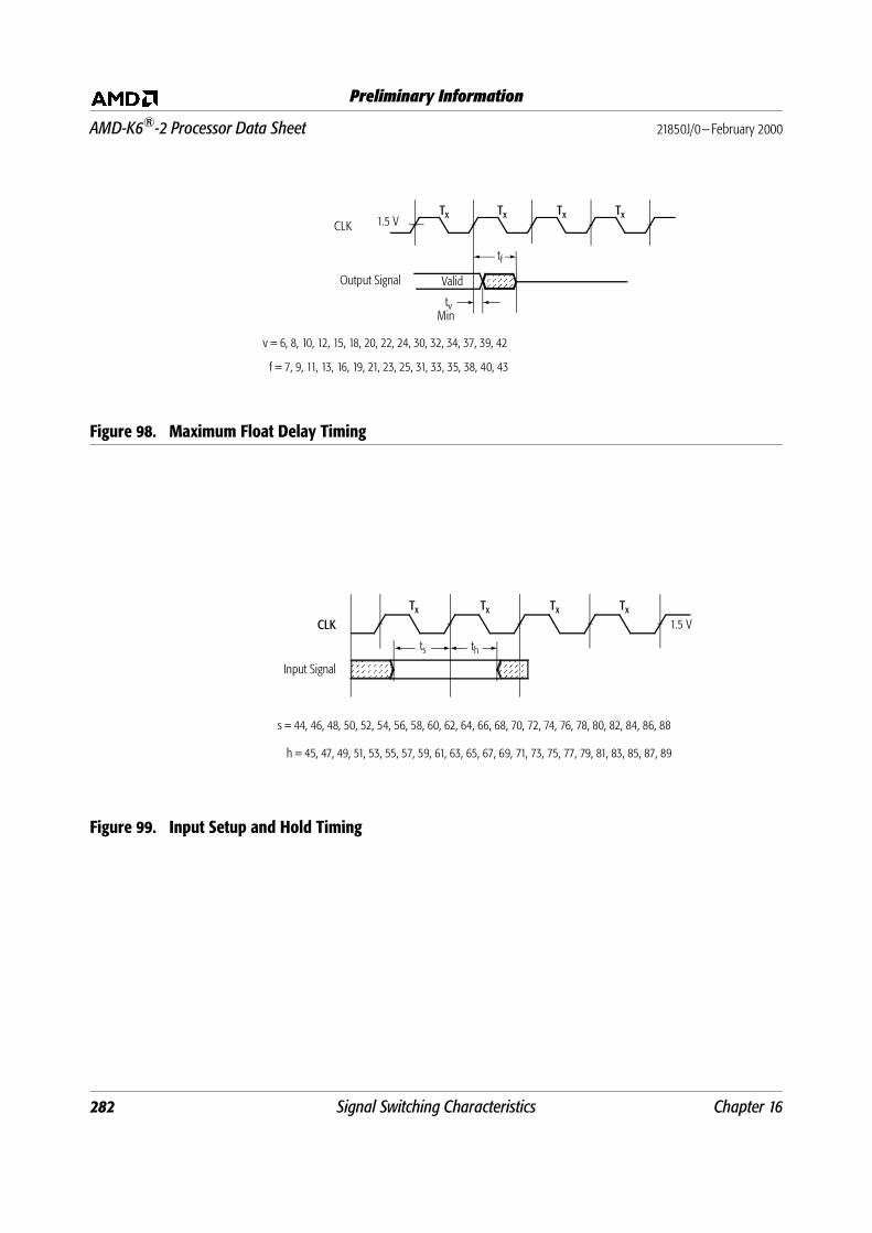
282 Signal Switching Characteristics Chapter 16
AMD-K6®-2 Processor Data Sheet 21850J/0—February 2000
Preliminary Information
Figure 98. Maximum Float Delay Timing
Figure 99. Input Setup and Hold Timing
Tx Tx Tx
Valid
Tx
tvMin
Output Signal
tf
CLK 1.5 V
v = 6, 8, 10, 12, 15, 18, 20, 22, 24, 30, 32, 34, 37, 39, 42
f = 7, 9, 11, 13, 16, 19, 21, 23, 25, 31, 33, 35, 38, 40, 43
CLK
Tx Tx Tx Tx
Input Signal
ts th
1.5 V
s = 44, 46, 48, 50, 52, 54, 56, 58, 60, 62, 64, 66, 68, 70, 72, 74, 76, 78, 80, 82, 84, 86, 88
h = 45, 47, 49, 51, 53, 55, 57, 59, 61, 63, 65, 67, 69, 71, 73, 75, 77, 79, 81, 83, 85, 87, 89

Chapter 16 Signal Switching Characteristics 283
21850J/0—February 2000 AMD-K6®-2 Processor Data Sheet
Preliminary Information
Figure 100. Reset and Configuration Timing
Tx
CLK
RESET
Tx
t90
FLUSH#
(Synchronous)
1.5 V
1.5 V1.5 V • • •t92, 93
t91
t99t100
• • •
BF[2:0]
(Asynchronous) t94
• • •
t95
FLUSH#, BRDYC#
(Asynchronous)t97, 101
t98, 102
• • •
• • •
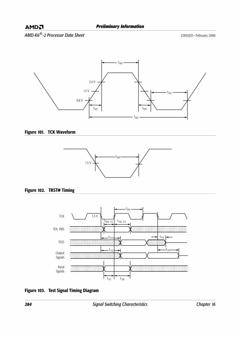
284 Signal Switching Characteristics Chapter 16
AMD-K6®-2 Processor Data Sheet 21850J/0—February 2000
Preliminary Information
Figure 101. TCK Waveform
Figure 102. TRST# Timing
Figure 103. Test Signal Timing Diagram
t107
2.0 V
1.5 V
0.8 V
t105
t106
t103
t104
1.5 V
t108
TCK
TDI, TMS
TDO
Output
Signals
Input
Signals
t103
t109, 111 t110, 112
t113
t115 t116
t117 t118
t114
1.5 V

Chapter 17 Thermal Design 285
21850J/0—February 2000 AMD-K6®-2 Processor Data Sheet
Preliminary Information
17 Thermal Design
17.1 Package Thermal Specifications
The AMD-K6-2 processor operating specification calls for the
case temperature (TC) to be in the range of 0°C to 70°C, 0°C to
65°C, or 0°C to 60°C. The ambient temperature (TA) is not
specified as long as the case temperature is not violated. The
case temperature must be measured on the top center of the
package. Table 71 and Table 72 show the AMD-K6-2 processor
thermal specifications for all valid OPN suffixes.
Table 71. Package Thermal Specification for OPN Suffixes AHX, AFQ, and AFR
θJC
Junction-Case
Maximum Thermal Power
2.2 V Component 2.4 V Component
266 MHz 300 MHz 333 MHz 350 MHz 366 MHz 380 MHz 400 MHz* 450 MHz 475 MHz
1.0 °C/W 14.70 W 17.20 W 19.00 W 19.95 W 20.80 W 21.60 W 22.70 W 28.40 W 29.60 W
Stop Grant Mode 3.90 W 3.92 W 3.94 W 3.96 W 3.96 W 3.97 W 3.98 W 6.50 W 6.51 W
Stop Clock Mode 3.50 W 3.50 W 3.50 W 3.50 W 3.50 W 3.50 W 3.50 W 6.00 W 6.00 W
TC Case Temperature 0°C–70°C 0°C–60°C 0°C–65°C
Note:
* Not applicable to OPN AMD-K6-2/400AFR. Refer to Table 72 on page 287 for the AMD-K6-2/400AFR specifications.

286 Thermal Design Chapter 17
AMD-K6®-2 Processor Data Sheet 21850J/0—February 2000
Preliminary Information

Chapter 17 Thermal Design 287
21850J/0—February 2000 AMD-K6®-2 Processor Data Sheet
Preliminary Information
Figure 104 on page 288 shows the thermal model of a processor
with a passive thermal solution. The case-to-ambient
temperature (TCA) can be calculated from the following
equation:
TCA = PMAX • θCA= PMAX • ( θIF + θSA)
Where:
PMAX = Maximum Power ConsumptionθCA = Case-to-Ambient Thermal ResistanceθIF = Interface Material Thermal ResistanceθSA = Sink-to-Ambient Thermal Resistance
Table 72. Package Thermal Specification for OPN Suffixes AGR, AFX, and 400AFR
θJC
Junction-Case
Maximum Thermal Power
2.2 V Component 2.3 V Component
400 MHz1 450 MHz 475 MHz 500 MHz 533 MHz2 550 MHz
1.0 °C/W 16.90 W 18.80 W 19.80 W 20.75 W 25.00 W
Stop Grant Mode 4.40 W 4.44 W 4.45 W 4.46 W 4.87 W
Stop Clock Mode 4.00 W 4.00 W 4.00 W 4.00 W 4.37 W
TC Case Temperature 0°C–70°C 0°C–65°C 0°C–70°C
Notes:
1. Specifications are applicable to OPN AMD-K6-2/400AFR.
2. The specifications provided for the 533 MHz component are identical to the specifications of the 500 MHzcomponent.

288 Thermal Design Chapter 17
AMD-K6®-2 Processor Data Sheet 21850J/0—February 2000
Preliminary Information
Figure 104. Thermal Model
Figure 105 illustrates the case-to-ambient temperature (TCA) in
relation to the power consumption (X-axis) and the thermal
resistance (Y-axis). If the power consumption and case
temperature are known, the thermal resistance (θCA)
requirement can be calculated for a given ambient temperature
(TA) value.
Figure 105. Power Consumption versus Thermal Resistance
TemperatureThermal
θSA θCA
θIF
(°C/W)(Ambient)
Case
Sink
TCA
Resistance
0.0
0.5
1.0
1.5
2.0
2.5
3.0
10 W 12 W 14 W 16 W 18 W 20 W 22 W 24 W 26 W 28 W 30 W 32 WPow er Cons um pt ion (Watt s )
The
rmal
Res
ista
nce
(deg
C/W
)
30 deg C
25 deg C
20 deg C
15 deg C
TCA = TC - TA
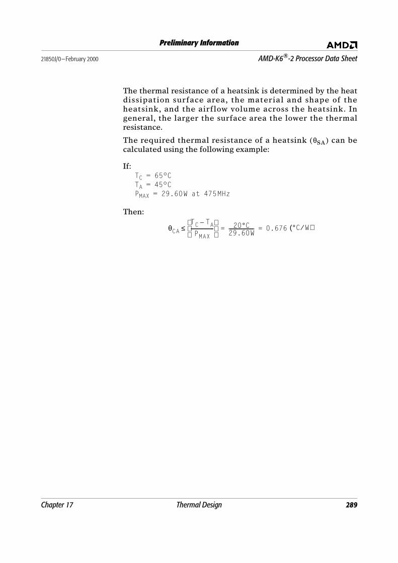
Chapter 17 Thermal Design 289
21850J/0—February 2000 AMD-K6®-2 Processor Data Sheet
Preliminary Information
The thermal resistance of a heatsink is determined by the heat
dissipation surface area, the material and shape of the
heatsink, and the airflow volume across the heatsink. In
general, the larger the surface area the lower the thermal
resistance.
The required thermal resistance of a heatsink (θSA) can be
calculated using the following example:
If:
TC = 65°C
TA = 45°C
PMAX = 29.60W at 475MHz
Then:
θCATC TA–
PMAX-------------------
≤ 20°C29.60W--------------------- 0.676 °C W⁄( )= =

290 Thermal Design Chapter 17
AMD-K6®-2 Processor Data Sheet 21850J/0—February 2000
Preliminary Information
Thermal grease is recommended as interface material because
it provides the lowest thermal resistance (≅ 0.20°C/W). The
required thermal resistance (θSA) of the heatsink in this
example is calculated as follows:
θSA = θCA – θIF = 0.676 – 0.20 = 0.476(°C/W)
Heat Dissipation Path Figure 106 illustrates the heat dissipation path of the processor.
Due to the lower thermal resistance between the processor die
junction and case, most of the heat generated by the processor
is transferred from the top surface of the case. The small
amount of heat generated from the bottom side of the processor
where the processor socket blocks the convection can be safely
ignored.
Figure 106. Processor Heat Dissipation Path
Measuring Case Temperature
The processor case temperature is measured to ensure that the
thermal so lut ion meets the processor ’s operat ional
specification. This temperature should be measured on the top
center of the package, where most of the heat is dissipated.
Figure 107 shows the correct location for measuring the case
temperature. If a heatsink is installed while measuring, the
thermocouple must be installed into the heatsink via a small
hole drilled through the heatsink base (for example, 1/16 of an
inch). The thermocouple is then attached to the base of the
heatsink and the small hole filled using thermal epoxy, allowing
the tip of the thermocouple to touch the top of the processor
case.
Thin LidCase temperature
Ambient Temperature
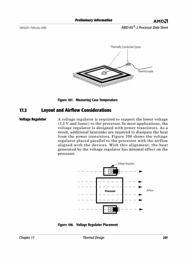
Chapter 17 Thermal Design 291
21850J/0—February 2000 AMD-K6®-2 Processor Data Sheet
Preliminary Information
Figure 107. Measuring Case Temperature
17.2 Layout and Airflow Considerations
Voltage Regulator A voltage regulator is required to support the lower voltage
(3.3 V and lower) to the processor. In most applications, the
voltage regulator is designed with power transistors. As a
result, additional heatsinks are required to dissipate the heat
from the power transistors. Figure 108 shows the voltage
regulator placed parallel to the processor with the airflow
aligned with the devices. With this alignment, the heat
generated by the voltage regulator has minimal effect on the
processor.
Figure 108. Voltage Regulator Placement
Thermocouple
Thermally Conductive Epoxy
Processor Airflow
Voltage Regulator

292 Thermal Design Chapter 17
AMD-K6®-2 Processor Data Sheet 21850J/0—February 2000
Preliminary Information
A heatsink and fan combination can deliver much better
thermal performance than a heatsink alone. More importantly,
with a fan/sink the airflow requirements in a system design are
not as critical. A unidirectional heatsink with a fan moves air
from the top of the heatsink to the side. In this case, the best
location for the voltage regulator is on the side of the processor
in the path of the airflow exiting the fan sink (see Figure 109).
This location guarantees that the heatsinks on both the
processor and the regulator receive adequate air circulation.
Figure 109. Airflow for a Heatsink with Fan
Airflow Management in a System Design
Complete airflow management in a system is important. In
addition to the volume of air, the path of the air is also
important. Figure 110 shows the airflow in a dual-fan system.
The fan in the front end pulls cool air into the system through
intake slots in the chassis. The power supply fan forces the hot
air out of the chassis. The thermal performance of the heatsink
can be maximized if it is located in the shaded area, where it
receives greatest benefit from this air exchange system.
Airflow
Ideal areas for voltage regulator

Chapter 17 Thermal Design 293
21850J/0—February 2000 AMD-K6®-2 Processor Data Sheet
Preliminary Information
Figure 110. Airflow Path in a Dual-Fan System
Figure 111 shows the airflow management in a system using the
ATX form-factor. The orientation of the power supply fan and
the motherboard are modified in the ATX platform design. The
power supply fan pulls cool air through the chassis and across
the processor. The processor is located near the power supply
fan, where it can receive adequate airflow without an auxiliary
fan. The arrangement significantly improves the airflow across
the processor with minimum installation cost.
Figure 111. Airflow Path in an ATX Form-Factor System
Drive Bays
P/S
Vents
Vents
Fan
Fan
Main Board
Front
P/S
Main Board
Drive Bays
Fan

294 Thermal Design Chapter 17
AMD-K6®-2 Processor Data Sheet 21850J/0—February 2000
Preliminary Information
For more information about thermal design considerations, see
the AMD-K6® Processor Thermal Solution Design Application
Note, order# 21085.
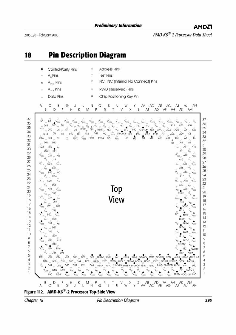
Chapter 18 Pin Description Diagram 295
21850J/0—February 2000 AMD-K6®-2 Processor Data Sheet
Preliminary Information
18 Pin Description Diagram
Figure 112. AMD-K6®-2 Processor Top-Side View

296 Pin Description Diagram Chapter 18
AMD-K6®-2 Processor Data Sheet 21850J/0—February 2000
Preliminary Information
Figure 113. AMD-K6®-2 Processor Pin-Side View

Chapter 19 Pin Designations 297
21850J/0—February 2000 AMD-K6®-2 Processor Data Sheet
Preliminary Information
19 Pin Designations
AMD-K6®-2 Processor Functional Grouping
Address Data Control Test NC Vcc2 Vcc3 Vss
Pin Name
PinNo.
Pin Name
PinNo.
PinName
PinNo.
PinName
PinNo.
PinNo.
PinNo.
PinNo.
PinNo.
A3A4A5A6A7A8A9A10A11A12A13A14A15A16A17A18A19A20A21A22A23A24A25A26A27A28A29A30A31
AL-35AM-34AK-32AN-33AL-33AM-32AK-30AN-31AL-31AL-29AK-28AL-27AK-26AL-25AK-24AL-23AK-22AL-21AF-34AH-36AE-33AG-35AJ-35AH-34AG-33AK-36AK-34AM-36AJ-33
D0D1D2D3D4D5D6D7D8D9D10D11D12D13D14D15D16D17D18D19D20D21D22D23D24D25D26D27D28D29D30D31D32D33D34D35D36D37D38D39D40D41D42D43D44D45D46D47D48D49D50D51D52D53D54D55D56D57D58D59D60D61D62D63
K-34G-35J-35G-33F-36F-34E-35E-33D-34C-37C-35B-36D-32B-34C-33A-35B-32C-31A-33D-28B-30C-29A-31D-26C-27C-23D-24C-21D-22C-19D-20C-17C-15D-16C-13D-14C-11D-12C-09D-10D-08A-05E-09B-04D-06C-05E-07C-03D-04E-05D-02F-04E-03G-05E-01G-03H-04J-03J-05K-04L-05L-03M-04N-03
A20M#ADS#ADSC#AHOLDAPCHK#BE0#BE1#BE2#BE3#BE4#BE5#BE6#BE7#BF0BF1BF2BOFF#BRDY#BRDYC#BREQCACHE#CLKD/C#EADS#EWBE#FERR#FLUSH#HIT#HITM#HLDAHOLDIGNNE#INITINTRINVKEN#LOCK#M/IO#NA#NMIPCDPCHK#PWTRESET SCYCSMI#SMIACT#STPCLK#VCC2DETVCC2H/L#W/R#WB/WT#
AK-08AJ-05AM-02V-04AE-05AL-09AK-10AL-11AK-12AL-13AK-14AL-15AK-16Y-33X-34W-35Z-04X-04Y-03AJ-01U-03AK-18AK-04AM-04W-03Q-05AN-07AK-06AL-05AJ-03AB-04AA-35AA-33AD-34U-05W-05AH-04T-04Y-05AC-33AG-05AF-04AL-03AK-20AL-17AB-34AG-03V-34AL-01AN-05AM-06AA-05
TCK M-34TDI N-35TDO N-33TMS P-34TRST# Q-33
Parity
AP AK-02DP0 D-36DP1 D-30DP2 C-25DP3 D-18DP4 C-07DP5 F-06DP6 F-02DP7 N-05
A-37E-17E-25R-34S-33S-35W-33AJ-15AJ-23AL-19AN-35
INC
C-01H-34Y-35Z-34AC-35AL-07AN-01AN-03
RSVD
J-33L-35P-04Q-03Q-35R-04S-03S-05AA-03AC-03AC-05AD-04AE-03AE-35
KEY
AH-32
A-07A-09A-11A-13A-15A-17B-02E-15G-01J-01L-01N-01Q-01S-01U-01W-01Y-01AA-01AC-01AE-01AG-01AJ-11AN-09AN-11AN-13AN-15AN-17AN-19
A-19A-21A-23A-25A-27A-29E-21E-27E-37G-37J-37L-33L-37N-37Q-37S-37T-34U-33U-37W-37Y-37AA-37AC-37AE-37AG-37AJ-19AJ-29AN-21AN-23AN-25AN-27AN-29
A-03 AM-20B-06 AM-22B-08 AM-24B-10 AM-26B-12 AM-28B-14 AM-30B-16 AN-37B-18B-20B-22B-24B-26B-28E-11E-13E-19E-23E-29E-31H-02H-36K-02K-36M-02M-36P-02P-36R-02R-36T-02T-36U-35V-02V-36X-02X-36Z-02Z-36AB-02AB-36AD-02AD-36AF-02AF-36AH-02AJ-07AJ-09AJ-13AJ-17AJ-21AJ-25AJ-27AJ-31AJ-37AL-37AM-08AM-10AM-12AM-14AM-16AM-18

298 Pin Designations Chapter 19
AMD-K6®-2 Processor Data Sheet 21850J/0—February 2000
Preliminary Information

Chapter 20 Package Specifications 299
21850J/0—February 2000 AMD-K6®-2 Processor Data Sheet
Preliminary Information
20 Package Specifications
20.1 321-Pin Staggered CPGA Package Specification
Table 73. 321-Pin Staggered CPGA Package Specification
SymbolMillimeters Inches
Min Max Notes Min Max Notes
A 49.28 49.78 1.940 1.960
B 45.59 45.85 1.795 1.805
C 31.01 32.89 1.221 1.295
D 44.90 45.10 1.768 1.776
E 2.91 3.63 0.115 0.143
F 1.30 1.52 0.051 0.060
G 3.05 3.30 0.120 0.130
H 0.43 0.51 0.017 0.020
M 2.29 2.79 0.090 0.110
N 1.14 1.40 0.045 0.055
d 1.52 2.29 0.060 0.090
e 1.52 2.54 0.060 0.100
f — 0.13 Flatness — 0.005 Flatness

300 Package Specifications Chapter 20
AMD-K6®-2 Processor Data Sheet 21850J/0—February 2000
Preliminary Information
Figure 114. 321-Pin Staggered CPGA Package Specification

Chapter 21 Ordering Information 301
21850J/0—February 2000 AMD-K6®-2 Processor Data Sheet
Preliminary Information
21 Ordering Information
Standard AMD-K6®-2 Processor Model 8 Products
AMD standard products are available in several operating ranges. The ordering part
number (OPN) is formed by a combination of the elements below.
Table 74. Valid Ordering Part Number Combinations
OPN Package Type Operating Voltage Case Temperature
AMD-K6-2/550AGR 321-pin CPGA2.2V–2.4V (Core)
3.135V–3.6V (I/O)0°C–70°C
AMD-K6-2/533AFX 321-pin CPGA2.1V–2.3V (Core)
3.135V–3.6V (I/O)0°C–65°C
AMD-K6-2/500AFX 321-pin CPGA2.1V–2.3V (Core)
3.135V–3.6V (I/O)0°C–65°C
Note:
This table lists configurations planned to be supported in volume for this device. Consult the local AMD sales office to confirm availability of specific valid combinations and to check on newly-released combinations.
AAMD-K6-2
Package Type
Family/Core
A = 321-pin CPGA
AMD-K6-2
Case TemperatureQ = 0°C–60°CR = 0°C–70°CX = 0°C–65°C
/550
Performance Rating/550/475/380/300
Operating Voltage
F = 2.1 V–2.3 V (Core) / 3.135 V–3.6 V (I/O)G = 2.2 V–2.4 V (Core) / 3.135 V–3.6 V (I/O)H = 2.3 V–2.5 V (Core) / 3.135 V–3.6 V (I/O)
G R
/533/450/350/266
/500/400/333
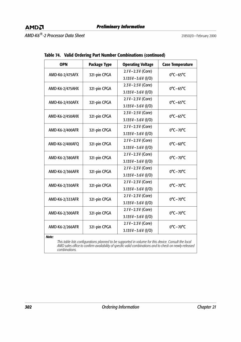
302 Ordering Information Chapter 21
AMD-K6®-2 Processor Data Sheet 21850J/0—February 2000
Preliminary Information
AMD-K6-2/475AFX 321-pin CPGA2.1V–2.3V (Core)
3.135V–3.6V (I/O)0°C–65°C
AMD-K6-2/475AHX 321-pin CPGA2.3V–2.5V (Core)
3.135V–3.6V (I/O)0°C–65°C
AMD-K6-2/450AFX 321-pin CPGA2.1V–2.3V (Core)
3.135V–3.6V (I/O)0°C–65°C
AMD-K6-2/450AHX 321-pin CPGA2.3V–2.5V (Core)
3.135V–3.6V (I/O)0°C–65°C
AMD-K6-2/400AFR 321-pin CPGA2.1V–2.3V (Core)
3.135V–3.6V (I/O)0°C–70°C
AMD-K6-2/400AFQ 321-pin CPGA2.1V–2.3V (Core)
3.135V–3.6V (I/O)0°C–60°C
AMD-K6-2/380AFR 321-pin CPGA2.1V–2.3V (Core)
3.135V–3.6V (I/O)0°C–70°C
AMD-K6-2/366AFR 321-pin CPGA2.1V–2.3V (Core)
3.135V–3.6V (I/O)0°C–70°C
AMD-K6-2/350AFR 321-pin CPGA2.1V–2.3V (Core)
3.135V–3.6V (I/O)0°C–70°C
AMD-K6-2/333AFR 321-pin CPGA2.1V–2.3V (Core)
3.135V–3.6V (I/O)0°C–70°C
AMD-K6-2/300AFR 321-pin CPGA2.1V–2.3V (Core)
3.135V–3.6V (I/O)0°C–70°C
AMD-K6-2/266AFR 321-pin CPGA2.1V–2.3V (Core)
3.135V–3.6V (I/O)0°C–70°C
Table 74. Valid Ordering Part Number Combinations (continued)
OPN Package Type Operating Voltage Case Temperature
Note:
This table lists configurations planned to be supported in volume for this device. Consult the local AMD sales office to confirm availability of specific valid combinations and to check on newly-released combinations.

Index 303
21850J/0—February 2000 AMD-K6®-2 Processor Data Sheet
Preliminary Information
Index
Numerics100-MHz Bus . . . . . . . . . . . . . . . . . . . . . . . . . . . . . . . . . . . . . 1, 3
clock switching characteristics . . . . . . . . . . . . . . . . . . . . 268input setup and hold timings. . . . . . . . . . . . . . . . . . . . . . 272output delay timings. . . . . . . . . . . . . . . . . . . . . . . . . . . . . 270
321-Pin Staggered CPGA Package . . . . . . . . . . . . . . . . . . . . . 1specification . . . . . . . . . . . . . . . . . . . . . . . . . . . . . . . . . . . 299
3DNow! Technology . . . . . .1–3, 7, 9–10, 13–17, 21, 54, 116, . . . . . . . . . . . . . . . . . . . . . . . . . . . . . . . . . 173, 177, 192
execution unit . . . . . . . . . . . . . . . . . . . . . . . . . . . . . . . . 16–17
instruction compatibility, floating-point and. . . . . . . . . 209
instructions . . . . . . . . . . . . . . . . . . . . . . . . . . . . . . . . . 81, 210
register operation . . . . . . . . . . . . . . . . . . . . . . . . . . . . . . . . . 8registers . . . . . . . . . . . . . . . . . . . . . . . . . . . . . . . . . . . . . . . . 29
66-MHz Busclock switching characteristics . . . . . . . . . . . . . . . . . . . . 268input setup and hold timings. . . . . . . . . . . . . . . . . . . . . . 276output delay timings. . . . . . . . . . . . . . . . . . . . . . . . . . . . . 274
AA[20:3] . . . . . . . . . . . . . . . . . . . . . . . . . . . . . . . . . . . . . . 263–264
A[31:3] . . . . . . . . . . . . . . . . . . . . . . . . . . . . . . . . . . . . . . . . . . . 86
A20M# . . . . . . . . . . . . . . . . . . . . . . . . . . . . . . . . . . . . . . . 85, 212
A20M# Masking of Cache Accesses . . . . . . . . . . . . . . . . . . 199
Absolute Ratings. . . . . . . . . . . . . . . . . . . . . . . . . . . . . . 254, 259
Accelerated Graphic Port (AGP) . . . . . . . . . . . . . . . . . . . . . 1, 3Acknowledge, Interrupt . . . . . . . . . . . . . . . . . . . . . . . . . . . . 162Address
bus . . . . . . . . . . . . . . . 86–91, 100, 127, 148, 152, 154, 194
hold. . . . . . . . . . . . . . . . . . . . . . . . . . . . . . . . . . . . . . . . . . . . 88parity . . . . . . . . . . . . . . . . . . . . . . . . . . . . . . . . . . . . . . . . . . 89parity check. . . . . . . . . . . . . . . . . . . . . . . . . . . . . . . . . . . . . 90stack, return . . . . . . . . . . . . . . . . . . . . . . . . . . . . . . . . . . . . 18
ADS# . . . . . . . . . . . . . . . . . . . . . . . . . . . . . . . . . . . .87, 263–264
ADSC# . . . . . . . . . . . . . . . . . . . . . . . . . . . . . . . . . . . . . . . . . . . 87
AGP . . . . . . . . . . . . . . . . . . . . . . . . . . . . . . . . . . . . . . . . . . . . 1, 3AHOLD . . . . . . . . . . . . . . . . . . . . . . . . . . . . . . . . . . . . . . 88, 244
-initiated inquire hit to modified line. . . . . . . . . . . . . . . 152-initiated inquire hit to shared or exclusive line . . . . . . 150-initiated inquire miss . . . . . . . . . . . . . . . . . . . . . . . . . . . 148restriction . . . . . . . . . . . . . . . . . . . . . . . . . . . . . . . . . . . . . 154
Airflowconsideration, layout and. . . . . . . . . . . . . . . . . . . . . . . . . 291management . . . . . . . . . . . . . . . . . . . . . . . . . . . . . . . . . . . 292
Allocate, Write . . . . . . . . . . . . . . . . . . . . . . . . . . . . . . . . . . . 186AP. . . . . . . . . . . . . . . . . . . . . . . . . . . . . . . . . . . . . . . . . . . . . . . 89APCHK#. . . . . . . . . . . . . . . . . . . . . . . . . . . . . . . . . . . . . . . . . . 90Architecture . . . . . . . . . . . . . . . . . . . . . . . . . . . . . . . . . . . . . . . 2
internal . . . . . . . . . . . . . . . . . . . . . . . . . . . . . . . . . . . . . . 5–19
Asserted . . . . . . . . . . . . . . . . . . . . . . . . . . . . . . . . . . . . . . . . . . 83
BBackoff . . . . . . . . . . . . . . . . . . . . . . . . . . . . . . . . . . . . . . . . . . . 93Base Address, SMM . . . . . . . . . . . . . . . . . . . . . . . . . . . . . . . 217BE[7:0]# . . . . . . . . . . . . . . . . . . . . . . . . . . . . . . . . . . . . . . . . . . 91
BF[2:0] . . . . . . . . . . . . . . . . . . . . . . . . . . . . . . . . . . 92, 173, 247
BIST. . . . . . . . . . . . . . . . . . . . . . . . . . . . . . . . . . . . . . . . . . . . 221
Bits, Predecode . . . . . . . . . . . . . . . . . . . . . . . . . . . . . . . 10, 180
Block Diagram . . . . . . . . . . . . . . . . . . . . . . . . . . . . . . . . . . . . . 6
BOFF# . . . . . . . . . . . . . . . . . . . . . . . . . . . . . . . . . . . . . . . 93, 156
locked operation with . . . . . . . . . . . . . . . . . . . . . . . . . . . 160Boundary Scan
register (BSR). . . . . . . . . . . . . . . . . . . . . . . . . . . . . . . . . . 225test access port (TAP) . . . . . . . . . . . . . . . . . . . . . . . . . . . 223
BR . . . . . . . . . . . . . . . . . . . . . . . . . . . . . . . . . . . . . . . . . . . . . 231Branch
execution unit . . . . . . . . . . . . . . . . . . . . . . . . . . . . . . . . . . 19history table . . . . . . . . . . . . . . . . . . . . . . . . . . . . . . . . . . . . 18logic . . . . . . . . . . . . . . . . . . . . . . . . . . . . . . . . . . . . . . . . . . . . 8
prediction . . . . . . . . . . . . . . . . . . . . . . . . . . . . . . . . 1–2, 9, 19
prediction logic . . . . . . . . . . . . . . . . . . . . . . . . . . . . . . 17–18
target cache . . . . . . . . . . . . . . . . . . . . . . . . . . . . . . . . . . . . 18BRDY#. . . . . . . . . . . . . . . . . . . . . . . . . . . . . . . . . . . . . . . . . . . 94
BRDYC# . . . . . . . . . . . . . . . . . . . . . . . . . . . . . . . . . 95, 173, 263
BREQ. . . . . . . . . . . . . . . . . . . . . . . . . . . . . . . . . . . . . . . . . . . . 96BSR . . . . . . . . . . . . . . . . . . . . . . . . . . . . . . . . . . . . . . . . . . . . 225Buffer Characteristics, I/O . . . . . . . . . . . . . . . . . . . . . . . . . 263Buffer Model, I/O . . . . . . . . . . . . . . . . . . . . . . . . . . . . . . . . . 264Built-In Self-Test . . . . . . . . . . . . . . . . . . . . . . . . . . . . . . . . . 221Burst
reads . . . . . . . . . . . . . . . . . . . . . . . . . . . . . . . . . . . . . . . . . 136reads, pipelined . . . . . . . . . . . . . . . . . . . . . . . . . . . . . . . . 136ready . . . . . . . . . . . . . . . . . . . . . . . . . . . . . . . . . . . . . . . . . . 94
ready copy. . . . . . . . . . . . . . . . . . . . . . . . . . . . . . . . . . 95, 173
writeback . . . . . . . . . . . . . . . . . . . . . . . . . . . . . . . . . . . . . 138Bus
100-MHz . . . . . . . . . . . . . . . . . . . . . . . . . . . . . . . . . . . . . . 1, 3address . . . . . . . . . . . . 88–91, 100, 127, 148, 152, 154, 194
arbitration cycles, inquire and . . . . . . . . . . . . . . . . . . . . 142backoff . . . . . . . . . . . . . . . . . . . . . . . . . . . . . . . . . . . . . . . 156cycles. . . . . . . . . . . . . . . . . . . . . . . . . . . . . . . . . . . . . . . . . 127cycles, special. . . . . . . . . . . . . . . . . . . . . . . . . . . . . . . . . . 164
data . 88, 91, 94, 98–99, 114, 117, 130–132, 148, 154, 158
enables . . . . . . . . . . . . . . . . . . . . . . . . . . . . . . . . . . . . . . . . 91frequency . . . . . . . . . . . . . . . . . . . . . . . . . . . . . . . . . . . . . . 92hold request . . . . . . . . . . . . . . . . . . . . . . . . . . . . . . . . . . . 105lock . . . . . . . . . . . . . . . . . . . . . . . . . . . . . . . . . . . . . . . . . . 110request . . . . . . . . . . . . . . . . . . . . . . . . . . . . . . . . . . . . . . . . 96state machine diagram . . . . . . . . . . . . . . . . . . . . . . . . . . 129
Bus Statesaddress . . . . . . . . . . . . . . . . . . . . . . . . . . . . . . . . . . . . . . . 130data . . . . . . . . . . . . . . . . . . . . . . . . . . . . . . . . . . . . . . . . . . 130data-NA# requested . . . . . . . . . . . . . . . . . . . . . . . . . . . . . 130idle. . . . . . . . . . . . . . . . . . . . . . . . . . . . . . . . . . . . . . . . . . . 130pipeline address . . . . . . . . . . . . . . . . . . . . . . . . . . . . . . . . 130pipeline data . . . . . . . . . . . . . . . . . . . . . . . . . . . . . . . . . . 131transition . . . . . . . . . . . . . . . . . . . . . . . . . . . . . . . . . . . . . 131
BYPASS Instruction. . . . . . . . . . . . . . . . . . . . . . . . . . . . . . . 232Bypass Register . . . . . . . . . . . . . . . . . . . . . . . . . . . . . . . . . . 231
CCache. . . . . . . . . . . . . . . . . . . . . . . . . . . . . . . . . . . . . . . . . . . . . 9
branch target . . . . . . . . . . . . . . . . . . . . . . . . . . . . . . . . . . . 18coherency . . . . . . . . . . . . . . . . . . . . . . . . . . . . . . . . . . . . . 194disabling . . . . . . . . . . . . . . . . . . . . . . . . . . . . . . . . . . . . . . 183enable . . . . . . . . . . . . . . . . . . . . . . . . . . . . . . . . . . . . . . . . 109

304 Index
AMD-K6®-2 Processor Data Sheet 21850J/0—February 2000
Preliminary Information
flush . . . . . . . . . . . . . . . . . . . . . . . . . . . . . . . . . . . . . . . . . . 103inhibit, L1 . . . . . . . . . . . . . . . . . . . . . . . . . . . . . . . . . . . . . 235
L1 . . . . . . . . . . . . . . . . . . . . . 1, 38, 179, 190, 194, 199, 221
MESI states in the data . . . . . . . . . . . . . . . . . . . . . . . . . . 180operation . . . . . . . . . . . . . . . . . . . . . . . . . . . . . . . . . . . . . . 181
organization. . . . . . . . . . . . . . . . . . . . . . . . . . . . . . . . 179, 201
snooping. . . . . . . . . . . . . . . . . . . . . . . . . . . . . . . . . . . . . . . 198states . . . . . . . . . . . . . . . . . . . . . . . . . . . . . . . . . . . . . . . . . 192
writeback . . . . . . . . . . . . . . . . . . . . . . . . . . . . . . . . . . . . . . 6, 9CACHE#. . . . . . . . . . . . . . . . . . . . . . . . . . . . . . . . . . . . . . 96, 183
Cacheableaccess . . . . . . . . . . . . . . . . . . . . . . . . . . . . . . . . . . . . . . . . . . 96page, write to a . . . . . . . . . . . . . . . . . . . . . . . . . . . . . . . . . 186
Cache-Linefills . . . . . . . . . . . . . . . . . . . . . . . . . . . . . . . . . . . . . . . . . . . 184
replacement. . . . . . . . . . . . . . . . . . . . . . . . . . . . . . . . 185, 196
Cache-Related Signals . . . . . . . . . . . . . . . . . . . . . . . . . . . . . 183Capture-DR state . . . . . . . . . . . . . . . . . . . . . . . . . . . . . . . . . 234Capture-IR state . . . . . . . . . . . . . . . . . . . . . . . . . . . . . . . . . . 234Case Temperature. . . . . . . . . . . . . . . . . . . . . . . . . . . . . . . . . 290Centralized Scheduler . . . . . . . . . . . . . . . . . . . . . . . . . . . . . . 14
Ceramic Pin Grid Array (CPGA) . . . . . . . . . . . . . . . . . . . 1, 299
CharacteristicsI/O buffer . . . . . . . . . . . . . . . . . . . . . . . . . . . . . . . . . . . . . . 263I/O Buffer AC and DC . . . . . . . . . . . . . . . . . . . . . . . . . . . . 265
CLK . . . . . . . . . . . . . . . . . . . . . . . . . . . . . . . . . . . . . . . . . . . . . 97Clock . . . . . . . . . . . . . . . . . . . . . . . . . . . . . . . . . . . . . . . . . . . . 97
control . . . . . . . . . . . . . . . . . . . . . . . . . . . . . . . . . . . . . . . . 243Clock States
halt . . . . . . . . . . . . . . . . . . . . . . . . . . . . . . . . . . . . . . . . . . . 244
stop clock . . . . . . . . . . . . . . . . . . . . . . . . . . . . . .167, 246–247
stop grant. . . . . . . . . . . . . . . . . . . . . . . . . . . . . . . . . . 167, 245
stop grant inquire . . . . . . . . . . . . . . . . . . . . . . . . . . . . . . . 246Coherency States, Writethrough vs. Writeback. . . . . . . . . 199Coherency, Cache . . . . . . . . . . . . . . . . . . . . . . . . . . . . . . . . . 194Compatibility, Floating-Point, MMX, and 3DNow!
Instructions . . . . . . . . . . . . . . . . . . . . . . . . . . . . . . . . 209Configuration and Initialization, Power-on . . . . . . . . . . . . 173Connection Requirements, Pin . . . . . . . . . . . . . . . . . . . . . . 251Connections, Power. . . . . . . . . . . . . . . . . . . . . . . . . . . . . . . . 249Control
register. . . . . . . . . . . . . . . . . . . . . . . . . . . . . . . . . . . . . . . . . 32unit, scheduler/instruction. . . . . . . . . . . . . . . . . . . . . . . . . . 8
Counter, Time Stamp . . . . . . . . . . . . . . . . . . . . . . . . . . . . . . . 38
CPGA . . . . . . . . . . . . . . . . . . . . . . . . . . . . . . . . . . . . 1, 299, 302
Cyclehold and hold acknowledge . . . . . . . . . . . . . . . . . . . . . . . 142shutdown . . . . . . . . . . . . . . . . . . . . . . . . . . . . . . . . . . . . . . 166
Cyclesbus . . . . . . . . . . . . . . . . . . . . . . . . . . . . . . . . . . . . . . . . . . . 127
inquire . . . . . . . .85–90, 100, 104–105, 118, 123, 138, 142, . . . . . . . 144, 146, 148, 150–152, 154, 156, 160, 194, . . . . . . . . . . . . . . . . . . . . . . . . . 197–199, 235, 243–246
inquire and bus arbitration . . . . . . . . . . . . . . . . . . . . . . . 142
interrupt acknowledge . . . . . . . . . . 86, 89, 91, 97, 112, 122
locked . . . . . . . . . . . . . . . . . . . . . . . . . . . . . . . . . . . . . . . . . 158
pipelined . . . . . . . . . . . . . . . . . . . . . . . . . . . . . . . . . . . .10, 87
pipelined write . . . . . . . . . . . . . . . . . . . . . . . . . . . . . . . . . . 98special bus . . . . . . . . . . . . . . . . . . . . . . . . . . . . . . . . . . . . . 164
writeback . . . . . . 85, 87–88, 101, 104, 123, 138, 146, 150, . . . . . . . . . . . . . . . . 152, 154, 156, 160, 183, 236, 246
DD/C# . . . . . . . . . . . . . . . . . . . . . . . . . . . . . . . . . . . . . . . . . . . . . 97
D[63:0]. . . . . . . . . . . . . . . . . . . . . . . . . . . . . . . . . . . . . . . . . . . 98Data
bus . . 88, 91, 94, 98–99, 114, 117, 130–132, 148, 154, 158
cache, MESI states in the . . . . . . . . . . . . . . . . . . . . . . . . 180parity. . . . . . . . . . . . . . . . . . . . . . . . . . . . . . . . . . . . . . . . . . 99
Data Types3DNow! . . . . . . . . . . . . . . . . . . . . . . . . . . . . . . . . . . . . . . . . 30floating-point register . . . . . . . . . . . . . . . . . . . . . . . . . . . . 28integer. . . . . . . . . . . . . . . . . . . . . . . . . . . . . . . . . . . . . . . . . 23MMX . . . . . . . . . . . . . . . . . . . . . . . . . . . . . . . . . . . . . . . . . . 29
Data/Code . . . . . . . . . . . . . . . . . . . . . . . . . . . . . . . . . . . . . . . . 97
DC Characteristics . . . . . . . . . . . . . . . . . . . . . . . . . . . . 254, 259
Debug . . . . . . . . . . . . . . . . . . . . . . . . . . . . . . . . . . . . . . . . . . 236exceptions. . . . . . . . . . . . . . . . . . . . . . . . . . . . . . . . . . . . . 241
Debug Registers . . . . . . . . . . . . . . . . . . . . . . . . . . . . . . . 34, 236
DR3–DR0 . . . . . . . . . . . . . . . . . . . . . . . . . . . . . . . . . . . . . 239DR5–DR4 . . . . . . . . . . . . . . . . . . . . . . . . . . . . . . . . . . . . . 239DR6 . . . . . . . . . . . . . . . . . . . . . . . . . . . . . . . . . . . . . . . . . . 240DR7 . . . . . . . . . . . . . . . . . . . . . . . . . . . . . . . . . . . . . . . . . . 240
Decode, Instruction . . . . . . . . . . . . . . . . . . . . . . . . . . . . . . . . 12Decoders . . . . . . . . . . . . . . . . . . . . . . . . . . . . . . . . . . . . . . . . . . 7Decoupling Recommendations. . . . . . . . . . . . . . . . . . . . . . 250Descriptions, Signal. . . . . . . . . . . . . . . . . . . . . . . . . . . . . . . . 83Design, Thermal. . . . . . . . . . . . . . . . . . . . . . . . . . . . . . . . . . 285Designations, Pin . . . . . . . . . . . . . . . . . . . . . . . . . . . . . . . . . 297Device Identification Register . . . . . . . . . . . . . . . . . . . . . . 230Diagram, Pin Description . . . . . . . . . . . . . . . . . . . . . . . . . . 295Diagrams, Timing. . . . . . . . . . . . . . . . . . . . . . . . . . . . . . . . . 127DIR . . . . . . . . . . . . . . . . . . . . . . . . . . . . . . . . . . . . . . . . . . . . 230Disabling, Cache . . . . . . . . . . . . . . . . . . . . . . . . . . . . . . . . . 183
Dissipation, Power . . . . . . . . . . . . . . . . . . . . . . . . . . . . 257, 262
DP[7:0] . . . . . . . . . . . . . . . . . . . . . . . . . . . . . . . . . . . . . . . . . . 99DR3–DR0 . . . . . . . . . . . . . . . . . . . . . . . . . . . . . . . . . . . . . . . 239DR5–DR4 . . . . . . . . . . . . . . . . . . . . . . . . . . . . . . . . . . . . . . . 239DR6 . . . . . . . . . . . . . . . . . . . . . . . . . . . . . . . . . . . . . . . . . . . . 240DR7 . . . . . . . . . . . . . . . . . . . . . . . . . . . . . . . . . . . . . . . . . . . . 240Drive Strength, Selectable . . . . . . . . . . . . . . . . . . . . . . . . . 263Driven . . . . . . . . . . . . . . . . . . . . . . . . . . . . . . . . . . . . . . . . . . . 83
EEADS#. . . . . . . . . . . . . . . . . . . . . . . . . . . . . . . . . . . . . . . . . . 100
EFER. . . . . . . . . . . . . . . . . . . . . . . . . . . . . 37, 39, 50, 176, 201
EFLAGS Register. . . . . . . . . . . . . . . . . . . . . . . . . . . . . . . . . . 31Electrical Data . . . . . . . . . . . . . . . . . . . . . . . . . . . . . . . . . . . 253Environment, Software . . . . . . . . . . . . . . . . . . . . . . . . . . . . . 21EWBE Control (EWBEC) . . . . . . . . . . . . . . . . . . . . . . . . . . 201
EWBE# . . . . . . . . . . . . . . . . . . . . . . . . . . . . . . . . . 101, 201, 244
Exception . . . . 89–90, 99, 102, 114, 166, 209, 220, 240–242
flags . . . . . . . . . . . . . . . . . . . . . . . . . . . . . . . . . . . . . . . . 26–27
floating-point . . . . . . . . . . . . . . . . . . . . . . 102, 106, 207–209
handler . . . . . . . . . . . . . . . . . . . . . . . . . . . . . . . . . . . . . . . 236machine check . . . . . . . . . . . . . . . . . . . . . . . . . . . . . . . . . . 37
Exceptionsand interrupts . . . . . . . . . . . . . . . . . . . . . . . . . . . . . . . . . . 49debug. . . . . . . . . . . . . . . . . . . . . . . . . . . . . . . . . . . . . . . . . 241floating-point . . . . . . . . . . . . . . . . . . . . . . . . . . . . . . . . . . 207handling floating-point . . . . . . . . . . . . . . . . . . . . . . . . . . 207interrupts, and debug in SMM . . . . . . . . . . . . . . . . . . . . 220MMX . . . . . . . . . . . . . . . . . . . . . . . . . . . . . . . . . . . . . . . . . 209
Execution Unit
3DNow! . . . . . . . . . . . . . . . . . . . . . . . . . . . . . . . . . . . 7, 16–17
branch . . . . . . . . . . . . . . . . . . . . . . . . . . . . . . . . . . . . 7, 14, 19
floating-point . . . . . . . . . . . . . . . . . . . . . . . . . . . 2, 7, 14, 207
load . . . . . . . . . . . . . . . . . . . . . . . . . . . . . . . . . . . . . . . . . 7, 14

Index 305
21850J/0—February 2000 AMD-K6®-2 Processor Data Sheet
Preliminary Information
multimedia . . . . . . . . . . . . . . . . . . . . . . 2, 7, 14, 16–17, 209
register X . . . . . . . . . . . . . . . . . . . . . . . . . . . . . . 7, 14, 16–17
register Y . . . . . . . . . . . . . . . . . . . . . . . . . . . . . . 7, 14, 16–17
store . . . . . . . . . . . . . . . . . . . . . . . . . . . . . . . . . . . . . . . . . 7, 14
Execution Units . . . . . . . . . . . . . . . . . . . . . . . . . . . . 1, 6–8, 15
Externaladdress strobe . . . . . . . . . . . . . . . . . . . . . . . . . . . . . . . . . . 100write buffer empty . . . . . . . . . . . . . . . . . . . . . . . . . . . . . . 101
EXTEST Instruction . . . . . . . . . . . . . . . . . . . . . . . . . . . . . . . 231
FFERR# . . . . . . . . . . . . . . . . . . . . . . . . . . . . . . . . . .102, 208–209
Fetch, Instruction . . . . . . . . . . . . . . . . . . . . . . . . . . . . . . . . . . 11
Float Conditions . . . . . . . . . . . . . . . . . . . . . . . . . . . . . . 122, 125
Floated . . . . . . . . . . . . . . . . . . . . . . . . . . . . . . . . . . . . . . . . . . . 83Floating-Point
and MMX/3DNow! instruction compatibility. . . . . . . . . 209and multimedia execution units . . . . . . . . . . . . . . . . . . . 207error . . . . . . . . . . . . . . . . . . . . . . . . . . . . . . . . . . . . . . . . . . 102execution unit . . . . . . . . . . . . . . . . . . . . . . . . . . . . . . . . . . 207handling exceptions . . . . . . . . . . . . . . . . . . . . . . . . . . . . . 207register data types . . . . . . . . . . . . . . . . . . . . . . . . . . . . . . . 28registers . . . . . . . . . . . . . . . . . . . . . . . . . . . . . . . . . . . . . . . . 25
FLUSH# . . . . . . . . . . . . . . . . . . . . . . . . 103, 173, 195, 222, 244
Frequency . . . . . . . . . . . . . . . . . . . . . . . . . . . . . . 247, 268, 280
operating . . . . . . . . . . . . . . . . . . . . . . . . . . . . . . . 92, 97, 173
Frequency Multiplier . . . . . . . . . . . . . . . . . . . . . . . . . . . . . . . 97Functional Unit. . . . . . . . . . . . . . . . . . . . . . . . . . . . . . . . . . . . 16
multimedia . . . . . . . . . . . . . . . . . . . . . . . . . . . . . . . . . . . . . 16
GGate Descriptor. . . . . . . . . . . . . . . . . . . . . . . . . . . . . . . . . 46, 49
General-Purpose Registers . . . . . . . . . . . . . . . . . . . . . . . . . . 22Global EWBE Disable (GEWBED) . . . . . . . . . . . . . . . . . . . 201Grounding, Power and . . . . . . . . . . . . . . . . . . . . . . . . . . . . . 249
HHalt State. . . . . . . . . . . . . . . . . . . . . . . . . . . . . . . . . . . . . . . . 244Handling Floating-Point Exceptions. . . . . . . . . . . . . . . . . . 207Heat Dissipation Path. . . . . . . . . . . . . . . . . . . . . . . . . . . . . . 290HIGHZ Instruction . . . . . . . . . . . . . . . . . . . . . . . . . . . . . . . . 232History Table, Branch . . . . . . . . . . . . . . . . . . . . . . . . . . . . . . . 18Hit to
modified line . . . . . . . . . . . . . . . . . . . . . . . . . . . . . . . . . . . 104modified line, AHOLD-initiated inquire . . . . . . . . . . . . 152modified line, HOLD-initiated inquire. . . . . . . . . . . . . . 146shared or exclusive line, AHOLD-initiated inquire. . . . 150shared or exclusive line, HOLD-initiated inquire . . . . . 144
HIT# . . . . . . . . . . . . . . . . . . . . . . . . . . . . . . . . . . . . . . . . . . . . 104
HITM# . . . . . . . . . . . . . . . . . . . . . . . . . . . . . . . . . .104, 263–264
HLDA . . . . . . . . . . . . . . . . . . . . . . . . . . . . . . . . . . . . . . . . . . . 105HOLD . . . . . . . . . . . . . . . . . . . . . . . . . . . . . . . . . . . . . . . . . . . 105
-initiated inquire hit to modified line. . . . . . . . . . . . . . . 146-initiated inquire hit to shared or exclusive line . . . . . . 144
Hold
acknowledge . . . . . . . . . . . . . . . . . . . . . . . . . . .105, 142–144
and hold acknowledge cycle . . . . . . . . . . . . . . . . . . . . . . 142
timing . . . . . . . . . . . . . . . . . . . . . . . . . . . . . . . . . . . . . 267, 282
II/O
buffer AC and DC characteristics . . . . . . . . . . . . . . . . . 265buffer characteristics . . . . . . . . . . . . . . . . . . . . . . . . . . . 263buffer model. . . . . . . . . . . . . . . . . . . . . . . . . . . . . . . . . . . 264misaligned read and write . . . . . . . . . . . . . . . . . . . . . . . 141model application note . . . . . . . . . . . . . . . . . . . . . . . . . . 265read and write . . . . . . . . . . . . . . . . . . . . . . . . . . . . . . . . . 140trap dword . . . . . . . . . . . . . . . . . . . . . . . . . . . . . . . . . . . . 218trap restart slot . . . . . . . . . . . . . . . . . . . . . . . . . . . . . . . . 219
IBIS . . . . . . . . . . . . . . . . . . . . . . . . . . . . . . . . . . . . . . . . . . . . 264IDCODE Instruction . . . . . . . . . . . . . . . . . . . . . . . . . . . . . . 232
IEEE 1149.1 . . . . . . . . . . . . . . . . . . . . . . . . . . . . . . . . . . . 1, 223
IEEE 754 . . . . . . . . . . . . . . . . . . . . . . . . . . . . . . . . . . . 1, 25, 207
IEEE 854 . . . . . . . . . . . . . . . . . . . . . . . . . . . . . . . . . . . . . . . . 207
IGNNE#. . . . . . . . . . . . . . . . . . . . . . . . . . . . . . . . . 106, 208–209
Ignore Numeric Exception . . . . . . . . . . . . . . . . . . . . . . . . . 106
INIT . . . . . . . . . . . . . . . . . . . . . . . . . . . . . . . . . . . . . . . . 107, 244
-initiated transition from protected mode to real mode 170state of processor after . . . . . . . . . . . . . . . . . . . . . . . . . . 177
Initialization . . . . . . . . . . . . . . . . . . . . . . . . . . . . . . . . . . . . . 107power-on configuration and . . . . . . . . . . . . . . . . . . . . . . 173
Input Setup and Hold Timings for100-MHz bus operation . . . . . . . . . . . . . . . . . . . . . . . . . . 27266-MHz bus operation . . . . . . . . . . . . . . . . . . . . . . . . . . . 276
Inquire . . . . . . . . . . . . . . . . . . . . . . . . . . . . . 145, 147, 149, 243
and bus arbitration cycles. . . . . . . . . . . . . . . . . . . . . . . . 142cycle hit. . . . . . . . . . . . . . . . . . . . . . . . . . . . . . . . . . . . . . . 104cycle hit to modified line . . . . . . . . . . . . . . . . . . . . . . . . 104
cycles.85–90, 100, 104–105, 118, 123, 138, 142, 144, 146, 148, . . . . 150–152, 154, 156, 160, 194, 197–199, 235, 243–. . . . . . . . . . . . . . . . . . . . . . . . . . . . . . . . . . . . . . 246
miss, AHOLD-initiated . . . . . . . . . . . . . . . . . . . . . . . . . . 148Instruction
decode. . . . . . . . . . . . . . . . . . . . . . . . . . . . . . . . . . . . . . . . . 12fetch . . . . . . . . . . . . . . . . . . . . . . . . . . . . . . . . . . . . . . . . . . 11pointer. . . . . . . . . . . . . . . . . . . . . . . . . . . . . . . . . . . . . . . . . 25prefetch. . . . . . . . . . . . . . . . . . . . . . . . . . . . . . . . . . . . . . . . . 9
Instructions
3DNow! . . . . . . . . . . . . . . . . . . . . . . . . . . . . . . . . . . . . 81, 209
EMMS . . . . . . . . . . . . . . . . . . . . . . . . . . . . . . . . . . . . . . . . . 14FEMMS . . . . . . . . . . . . . . . . . . . . . . . . . . . . . . . . . . . . . . . . 14INVD . . . . . . . . . . . . . . . . . . . . . . . . . . . . . . . . . . . . . . . . . 196
MMX . . . . . . . . . . . . . . . . . . . . . . . . . . . . . . . . . . . . . . 78, 209
PREFETCH . . . . . . . . . . . . . . . . . . . . . . . . . . . . . . . . 10, 192
supported by the AMD-K6-2 processor . . . . . . . . . . . . . . 54TAP . . . . . . . . . . . . . . . . . . . . . . . . . . . . . . . . . . . . . . . . . . 231WBINVD . . . . . . . . . . . . . . . . . . . . . . . . . . . . . . . . . . . . . . 196
Integer Data Types. . . . . . . . . . . . . . . . . . . . . . . . . . . . . . . . . 23Internal
architecture . . . . . . . . . . . . . . . . . . . . . . . . . . . . . . . . . . 5–19
snooping . . . . . . . . . . . . . . . . . . . . . . . . . . . . . . . . . . . . . . 194
Interrupt . . . . . . . . . . . . . . 108, 117, 162, 166–167, 170, 177,. . . . . . . . . . . . . . . . . . . . . 207–209, 212, 220, 241, 246
acknowledge . . . . . . . . . 86, 94, 97, 108, 110, 114, 158, 162
acknowledge cycles . . . . . . . . . . . . 86, 89, 91, 97, 112, 122
descriptor table register . . . . . . . . . . . . . . . . . . . . . . . 40–41
flag. . . . . . . . . . . . . . . . . . . . . . . . . . . . . . . . . . . . . . . 108, 117
flags . . . . . . . . . . . . . . . . . . . . . . . . . . . . . . . . . . . . . . . . . . . 31gate . . . . . . . . . . . . . . . . . . . . . . . . . . . . . . . . . . . . . . . . . . . 48redirection bitmap. . . . . . . . . . . . . . . . . . . . . . . . . . . . . . . 42request . . . . . . . . . . . . . . . . . . . . . . . . . . . . . . . . . . . . . . . 108
service routine . . . . . . . . . . . . . . . . . . . . . 108, 112, 208, 211
system management . . . . . . . . . . . . . . . . . . . . . . . . . . . . 211

306 Index
AMD-K6®-2 Processor Data Sheet 21850J/0—February 2000
Preliminary Information
type of . . . . . . . . . . . . . . . . . . . . . . . . . . . . . . . . . . . . . . . . . 49Interrupts
01h . . . . . . . . . . . . . . . . . . . . . . . . . . . . . . . . . . . . . . . . . . . 24203h . . . . . . . . . . . . . . . . . . . . . . . . . . . . . . . . . . . . . . . . . . . 24210h . . . . . . . . . . . . . . . . . . . . . . . . . . . . . . . . . . . . . . . . . . . 207exceptions and . . . . . . . . . . . . . . . . . . . . . . . . . . . . . . . . . . 49INTR. . . . . . . . . . . . . . . . . . . . . . . . . . . . . . . . . . . . . . . . . . 108IRQ13 . . . . . . . . . . . . . . . . . . . . . . . . . . . . . . . . . . . . . . . . . 208NMI. . . . . . . . . . . . . . . . . . . . . . . . . . . . . . . . . . . . . . . . . . . 112
INTR. . . . . . . . . . . . . . . . . . . . . . . . . . . . . . . . . . . . . . . . 108, 244
INV . . . . . . . . . . . . . . . . . . . . . . . . . . . . . . . . . . . . . . . . . . . . . 108Invalidation Request . . . . . . . . . . . . . . . . . . . . . . . . . . . . . . 108INVD Instruction . . . . . . . . . . . . . . . . . . . . . . . . . . . . . . . . . 196
KKEN# . . . . . . . . . . . . . . . . . . . . . . . . . . . . . . . . . . . . . . . 109, 186
LL1 Cache . . . . . . . . . . . . . . . . . . . . . . 1, 38, 179, 190, 199, 221
inhibit. . . . . . . . . . . . . . . . . . . . . . . . . . . . . . . . . . . . . . . . . 235Limit, Write Allocate . . . . . . . . . . . . . . . . . . . . . . . . . . . . . . 187Line Fills, Cache- . . . . . . . . . . . . . . . . . . . . . . . . . . . . . . . . . 184LOCK# . . . . . . . . . . . . . . . . . . . . . . . . . . . . . . . . . . . . . . . . . . 110Locked
cycles . . . . . . . . . . . . . . . . . . . . . . . . . . . . . . . . . . . . . . . . . 158operation with BOFF# intervention . . . . . . . . . . . . . . . . 160operation, basic. . . . . . . . . . . . . . . . . . . . . . . . . . . . . . . . . 158
Logicbranch . . . . . . . . . . . . . . . . . . . . . . . . . . . . . . . . . . . . . . . . . . 8
branch-prediction . . . . . . . . . . . . . . . . . . . . . . . . . . . . . 17–18
external support of floating-point exceptions . . . . . . . . 207
MM/IO# . . . . . . . . . . . . . . . . . . . . . . . . . . . . . . . . . . . . . . . . . . . 111Machine Check Exception . . . . . . . . . . . . . . . . . . . . . . . . . . . 37Maskable Interrupt. . . . . . . . . . . . . . . . . . . . . . . . . . . . . . . . 108
MCAR. . . . . . . . . . . . . . . . . . . . . . . . . . . . . . . . . . . . 37, 50, 176
MCTR . . . . . . . . . . . . . . . . . . . . . . . . . . . . . . . . . 37–38, 50, 176
Memoryor I/O . . . . . . . . . . . . . . . . . . . . . . . . . . . . . . . . . . . . . . . . . 111read and write, misaligned single-transfer . . . . . . . . . . 134read and write, single-transfer . . . . . . . . . . . . . . . . . . . . 132reads and writes . . . . . . . . . . . . . . . . . . . . . . . . . . . . . . . . 132
type range register (MTRR) . . . . . . . . . . 52, 189–190, 203
MESI. . . . . . . . . . . . . . . . . . 1, 9, 142, 146, 180, 192, 197, 199
bit . . . . . . . . . . . . . . . . . . . . . . . . . . . . . . . . . . . . . . . . . 10, 180
states in the data cache . . . . . . . . . . . . . . . . . . . . . . . . . . 180Microarchitecture . . . . . . . . . . . . . . . . . . . . . . . . . . . . . . . . . . . 2
enhanced RISC86 . . . . . . . . . . . . . . . . . . . . . . . . . . . . . . . . . 6overview, AMD-K6-2 processor . . . . . . . . . . . . . . . . . . . . . . 5
MisalignedI/O read and write. . . . . . . . . . . . . . . . . . . . . . . . . . . . . . . 141single-transfer memory read and write . . . . . . . . . . . . . 134
MMX Technology . . . . . . . . . . . .13–17, 21, 54, 116, 173, 177
exceptions . . . . . . . . . . . . . . . . . . . . . . . . . . . . . . . . . . . . . 209instruction compatibility, floating-point and. . . . . . . . . 209
instructions . . . . . . . . . . . . . . . . . . . . . . . . . . . . . . . . . 78, 210
register operation . . . . . . . . . . . . . . . . . . . . . . . . . . . . . . . . . 8registers . . . . . . . . . . . . . . . . . . . . . . . . . . . . . . . . . . . . . . . . 29
Mode, Tri-State Test . . . . . . . . . . . . . . . . . . . . . . . . . . . . . . . 222Model-Specific Registers (MSR) . . . . . . . . . . . . . . . . . . . . . . 37MSR . . . . . . . . . . . . . . . . . . . . . . . . . . . . . . . . . . . . . . . . . . . . . 37
MTRR . . . . . . . . . . . . . . . . . . . . . . . . . . . . . . . 52, 189–190, 203
Multimedia
execution unit . . . . . . . . . . . . . . . . . . . . . . . . . . . 16–17, 209
functional unit . . . . . . . . . . . . . . . . . . . . . . . . . . . . . . . . . . 16
NNA# . . . . . . . . . . . . . . . . . . . . . . . . . . . . . . . . . . . . . . . . . . . . 112Negated. . . . . . . . . . . . . . . . . . . . . . . . . . . . . . . . . . . . . . . . . . 83Next Address . . . . . . . . . . . . . . . . . . . . . . . . . . . . . . . . . . . . 112
NMI . . . . . . . . . . . . . . . . . . . . . . . . . . . . . . . . . . . . . . . . 112, 244
No-Connect Pins. . . . . . . . . . . . . . . . . . . . . . . . . . . . . . 116, 251
Non-Maskable Interrupt . . . . . . . . . . . . . . . . . . . . . . . . . . . 112Non-Pipelined. . . . . . . . . . . . . . . . . . . . . . . . . . . . . . . . . . . . 133
OOperating Ranges . . . . . . . . . . . . . . . . . . . . . . . . . . . . 253, 258
Operation, Cache . . . . . . . . . . . . . . . . . . . . . . . . . . . . . . . . . 181
Organization, Cache. . . . . . . . . . . . . . . . . . . . . . . . . . . 179, 201
Output Delay Timingsfor 100-MHz bus operation . . . . . . . . . . . . . . . . . . . . . . . 270for 66-MHz bus operation . . . . . . . . . . . . . . . . . . . . . . . . 274
Output Signals . . . . . . . . . . . . . . . . . . . . . . . . . . . . . . . . . . . 174
PPackage
specifications . . . . . . . . . . . . . . . . . . . . . . . . . . . . . . . . . . 299thermal specifications . . . . . . . . . . . . . . . . . . . . . . . . . . . 285
Pagecache disable . . . . . . . . . . . . . . . . . . . . . . . . . . . . . . . . . . 113
directory entry (PDE) . . . . . . . . . . . . . . . . . . . . . 44–45, 182
table entry (PTE) . . . . . . . . . . . . . . . . . . . . . . . . . 44, 46, 182
writethrough. . . . . . . . . . . . . . . . . . . . . . . . . . . . . . . . . . . 115Paging . . . . . . . . . . . . . . . . . . . . . . . . . . . . . . . . . . . . . . . . . . . 43
Parity. . . . . . . . . . . . . . . . . . . . . . . . . . 84, 89, 91, 99, 114, 132
bit . . . . . . . . . . . . . . . . . . . . . . . . . . . . . . . . . . . . . 89, 99, 114
check . . . . . . . . . . . . . . . . . . . . . . . . . . . . . . . . 89–90, 99, 114
error . . . . . . . . . . . . . . . . . . . . . . . . . . . . . . 90, 114, 148, 224
flags . . . . . . . . . . . . . . . . . . . . . . . . . . . . . . . . . . . . . . . . . . . 31
PCD . . . . . . . . . . . . . . . . . . . . . . . . . . . . . . . . . . . . 113, 182, 190
PCHK# . . . . . . . . . . . . . . . . . . . . . . . . . . . . . . . . . . . . . . . . . 114
PFIR . . . . . . . . . . . . 50, 53, 175–176, 184, 195–197, 199, 236
Pinconnection requirements . . . . . . . . . . . . . . . . . . . . . . . . 251description diagram. . . . . . . . . . . . . . . . . . . . . . . . . . . . . 295designations . . . . . . . . . . . . . . . . . . . . . . . . . . . . . . . . . . . 297
Pipeline. . . . . . . . . . . . . . . . . . . . . . . . . . . . . . 18, 130–131, 136
control . . . . . . . . . . . . . . . . . . . . . . . . . . . . . . . . . . . . . . . . . 16register X and Y. . . . . . . . . . . . . . . . . . . . . . . . . . . . . . . . . 16
six-stage . . . . . . . . . . . . . . . . . . . . . . . . . . . . . . . . . . . . . . 6, 8Pipelined. . . . . . . . . .9, 16, 112, 131, 136–137, 154, 179, 192
burst reads . . . . . . . . . . . . . . . . . . . . . . . . . . . . . . . . . . . . 136
cycles. . . . . . . . . . . . . . . . . . . . . . . . . . . . . . . . . . . . 10, 87, 98
design . . . . . . . . . . . . . . . . . . . . . . . . . . . . . . . . . . . . . . . . . 15Pointer, Instruction . . . . . . . . . . . . . . . . . . . . . . . . . . . . . . . . 25Power
and grounding . . . . . . . . . . . . . . . . . . . . . . . . . . . . . . . . . 249connections. . . . . . . . . . . . . . . . . . . . . . . . . . . . . . . . . . . . 249
dissipation . . . . . . . . . . . . . . . . . . . . . . . . . . . . . . . . 257, 262
Power-on Configuration and Initialization . . . . . . . . . . . . 173
Predecode Bits . . . . . . . . . . . . . . . . . . . . . . . . . . . . . . 9–10, 180

Index 307
21850J/0—February 2000 AMD-K6®-2 Processor Data Sheet
Preliminary Information
Prefetching . . . . . . . . . . . . . . . . . . . . . . . . . . . . . . . . . . .10, 192
PSOR . . . . . . . . . . . . . . . . . . . . . . . . . . . . . . . . 50, 53, 175–176
PWT Instruction . . . . . . . . . . . . . . . . . . . . . . . . . . . . . . . . . . 115
RRanges, Operating . . . . . . . . . . . . . . . . . . . . . . . . . . . . 253, 258
Ratings, Absolute . . . . . . . . . . . . . . . . . . . . . . . . . . . . . 254, 259
Read and Writebasic I/O . . . . . . . . . . . . . . . . . . . . . . . . . . . . . . . . . . . . . . . 140misaligned I/O . . . . . . . . . . . . . . . . . . . . . . . . . . . . . . . . . . 141
Reads, Burst Reads and Pipelined Burst . . . . . . . . . . . . . . 136Register
boundary scan . . . . . . . . . . . . . . . . . . . . . . . . . . . . . . . . . . 225bypass (BR) . . . . . . . . . . . . . . . . . . . . . . . . . . . . . . . . . . . . 231control . . . . . . . . . . . . . . . . . . . . . . . . . . . . . . . . . . . . . . . . . 32data Types, floating-point . . . . . . . . . . . . . . . . . . . . . . . . . 28
debug . . . . . . . . . . . . . . . . . . . . . . . . . . . . . . . . . . . . . . 34, 236
floating-point. . . . . . . . . . . . . . . . . . . . . . . . . . . . . . . . . . . . 25general-purpose. . . . . . . . . . . . . . . . . . . . . . . . . . . . . . . . . . 22SYSCALL/SYSRET Target Address (STAR) . . . . . . . . . . 39
Register X . . . . . . . . . . . . . . . . . . . . . . . . . . . . . . . . . . . . . . . . 16execution unit . . . . . . . . . . . . . . . . . . . . . . . . . . . . . . . . . . . 17
Register X and Ypipelines . . . . . . . . . . . . . . . . . . . . . . . . . . . . . . . . . . . . . . . 16
Register Y . . . . . . . . . . . . . . . . . . . . . . . . . . . . . . . . . . . . . . . . 16execution unit . . . . . . . . . . . . . . . . . . . . . . . . . . . . . . . . . . . 17
Registers . . . . . . . . . . . . . . . . . . . . . . . . . . . . . . 8, 21, 174, 209
3DNow!. . . . . . . . . . . . . . . . . . . . . . . . . . . . . . . . . . . . . . 21, 29
descriptors and gates . . . . . . . . . . . . . . . . . . . . . . . . . . . . . 46device identification (DIR) . . . . . . . . . . . . . . . . . . . . . . . 230DR3–DR0 . . . . . . . . . . . . . . . . . . . . . . . . . . . . . . . . . . . . . . 239DR5–DR4 . . . . . . . . . . . . . . . . . . . . . . . . . . . . . . . . . . . . . . 239DR6. . . . . . . . . . . . . . . . . . . . . . . . . . . . . . . . . . . . . . . . . . . 240DR7. . . . . . . . . . . . . . . . . . . . . . . . . . . . . . . . . . . . . . . . . . . 240EFLAGS . . . . . . . . . . . . . . . . . . . . . . . . . . . . . . . . . . . . . . . . 31
extended feature enable register (EFER) . . . . . . . . . 39, 50
IR . . . . . . . . . . . . . . . . . . . . . . . . . . . . . . . . . . . . . . . . . . . . 224MCAR. . . . . . . . . . . . . . . . . . . . . . . . . . . . . . . . . . . . . . . . . . 37memory management . . . . . . . . . . . . . . . . . . . . . . . . . . . . . 40
MMX. . . . . . . . . . . . . . . . . . . . . . . . . . . . . . . . . . . . . . . . 21, 29
PFIR . . . . . . . . . . . . . . . . . . . . . . . . . . . . . . . . . . . . . . . . . . . 53PSOR . . . . . . . . . . . . . . . . . . . . . . . . . . . . . . . . . . . . . . . . . . 53segment . . . . . . . . . . . . . . . . . . . . . . . . . . . . . . . . . . . . . . . . 24STAR . . . . . . . . . . . . . . . . . . . . . . . . . . . . . . . . . . . . . . . . . . 39TAP. . . . . . . . . . . . . . . . . . . . . . . . . . . . . . . . . . . . . . . . . . . 224TR12. . . . . . . . . . . . . . . . . . . . . . . . . . . . . . . . . . . . . . . . . . . 38UWCCR . . . . . . . . . . . . . . . . . . . . . . . . . . . . . . . . . . . . . . . . 52
WHCR . . . . . . . . . . . . . . . . . . . . . . . . . . . . . . . . . . . . . . 40, 51
X and Y . . . . . . . . . . . . . . . . . . . . . . . . . . . . . . . . . . . . . 14–16
Regulator, Voltage . . . . . . . . . . . . . . . . . . . . . . . . . . . . . . . . 291
Replacement, Cache-Line . . . . . . . . . . . . . . . . . . . . . . 185, 196
Requirements, Pin Connection . . . . . . . . . . . . . . . . . . . . . . 251Reserved . . . . . . . . . . . . . . . . . . . . . . . . . . . . . . . . . . . . . . . . 116
RESET . . . . . . . . . . . . . . . . . . . . . . . . . . . . . . . . . 116, 174, 244
and Test Signal Timing. . . . . . . . . . . . . . . . . . . . . . . . . . . 278signals sampled during. . . . . . . . . . . . . . . . . . . . . . . . . . . 173state of processor after. . . . . . . . . . . . . . . . . . . . . . . . . . . 174
Return Address Stack. . . . . . . . . . . . . . . . . . . . . . . . . . . . . . . 18Revision Identifier, SMM . . . . . . . . . . . . . . . . . . . . . . . . . . . 216RISC86 Microarchitecture . . . . . . . . . . . . . . . . . . . . . . . . . . . . 6
RSM Instruction . . . . . . . . . . . . . . . . . . . . . . . . . . . . . . 217, 220
RSVD . . . . . . . . . . . . . . . . . . . . . . . . . . . . . . . . . . . . . . . . . . . 116
SSAMPLE/PRELOAD Instruction . . . . . . . . . . . . . . . . . . . . 232Sampled . . . . . . . . . . . . . . . . . . . . . . . . . . . . . . . . . . . . . . . . . 83Scheduler
centralized . . . . . . . . . . . . . . . . . . . . . . . . . . . . . . . . . . . . . 14instruction control unit . . . . . . . . . . . . . . . . . . . . . . . . . . . . 8
SCYC . . . . . . . . . . . . . . . . . . . . . . . . . . . . . . . . . . . . . . . . . . . 117Sector, Write to a . . . . . . . . . . . . . . . . . . . . . . . . . . . . . . . . . 187Segment
descriptor . . . . . . . . . . . . . . . . . . . . . . . . . . . . . . . . 24, 46–48
registers . . . . . . . . . . . . . . . . . . . . . . . . . . . . . . . . . . . . . . . 24task state. . . . . . . . . . . . . . . . . . . . . . . . . . . . . . . . . . . . . . . 42usage . . . . . . . . . . . . . . . . . . . . . . . . . . . . . . . . . . . . . . . . . . 24
Selectable Drive Strength . . . . . . . . . . . . . . . . . . . . . . . . . . 263Shift-DR state. . . . . . . . . . . . . . . . . . . . . . . . . . . . . . . . . . . . 234Shift-IR state . . . . . . . . . . . . . . . . . . . . . . . . . . . . . . . . . . . . 234Shutdown Cycle . . . . . . . . . . . . . . . . . . . . . . . . . . . . . . . . . . 166Signal
descriptions . . . . . . . . . . . . . . . . . . . . . . . . . . . . . . . . . . . . 83switching characteristics . . . . . . . . . . . . . . . . . . . . . . . . . 267terminology. . . . . . . . . . . . . . . . . . . . . . . . . . . . . . . . . . . . . 83timing, RESET and test. . . . . . . . . . . . . . . . . . . . . . . . . . 278
Signals
A[20:3]. . . . . . . . . . . . . . . . . . . . . . . . . . . . . . . . . . . . 263–264
A[31:3]. . . . . . . . . . . . . . . . . . . . . . . . . . . . . . . . . . . . . . . . . 86
A20M#. . . . . . . . . . . . . . . . . . . . . . . . . . . . . . . . . . . . . 85, 212
ADS# . . . . . . . . . . . . . . . . . . . . . . . . . . . . . . . . . . 87, 263–264
ADSC#. . . . . . . . . . . . . . . . . . . . . . . . . . . . . . . . . . . . . . . . . 87
AHOLD . . . . . . . . . . . . . . . . . . . . . . . . . . . . . . . . . . . . 88, 244
AP . . . . . . . . . . . . . . . . . . . . . . . . . . . . . . . . . . . . . . . . . . . . 89APCHK# . . . . . . . . . . . . . . . . . . . . . . . . . . . . . . . . . . . . . . . 90BE[7:0]# . . . . . . . . . . . . . . . . . . . . . . . . . . . . . . . . . . . . . . . 91
BF[2:0]. . . . . . . . . . . . . . . . . . . . . . . . . . . . . . . . . . . . . 92, 247
BOFF# . . . . . . . . . . . . . . . . . . . . . . . . . . . . . . . . . . . . . 93, 156
BRDY#. . . . . . . . . . . . . . . . . . . . . . . . . . . . . . . . . . . . . . . . . 94
BRDYC# . . . . . . . . . . . . . . . . . . . . . . . . . . . . . . . . . . . 95, 263
BREQ. . . . . . . . . . . . . . . . . . . . . . . . . . . . . . . . . . . . . . . . . . 96
CACHE# . . . . . . . . . . . . . . . . . . . . . . . . . . . . . . . . . . . 96, 183
cache-related . . . . . . . . . . . . . . . . . . . . . . . . . . . . . . . . . . 183CLK . . . . . . . . . . . . . . . . . . . . . . . . . . . . . . . . . . . . . . . . . . . 97D/C#. . . . . . . . . . . . . . . . . . . . . . . . . . . . . . . . . . . . . . . . . . . 97D[63:0]. . . . . . . . . . . . . . . . . . . . . . . . . . . . . . . . . . . . . . . . . 98DP[7:0] . . . . . . . . . . . . . . . . . . . . . . . . . . . . . . . . . . . . . . . . 99EADS#. . . . . . . . . . . . . . . . . . . . . . . . . . . . . . . . . . . . . . . . 100
EWBE# . . . . . . . . . . . . . . . . . . . . . . . . . . . . . . . 101, 201, 244
FERR#. . . . . . . . . . . . . . . . . . . . . . . . . . . . . . . . . . . . 102, 209
FLUSH# . . . . . . . . . . . . . . . . . . . . . 103, 173, 195, 222, 244
HIT# . . . . . . . . . . . . . . . . . . . . . . . . . . . . . . . . . . . . . . . . . 104
HITM#. . . . . . . . . . . . . . . . . . . . . . . . . . . . . . . . 104, 263–264
HLDA . . . . . . . . . . . . . . . . . . . . . . . . . . . . . . . . . . . . . . . . 105HOLD . . . . . . . . . . . . . . . . . . . . . . . . . . . . . . . . . . . . . . . . 105
IGNNE#. . . . . . . . . . . . . . . . . . . . . . . . . . . . . . . . . . . 106, 209
INIT . . . . . . . . . . . . . . . . . . . . . . . . . . . . . . . . . . . . . . 107, 244
INTR . . . . . . . . . . . . . . . . . . . . . . . . . . . . . . . . . . . . . 108, 244
INV . . . . . . . . . . . . . . . . . . . . . . . . . . . . . . . . . . . . . . . . . . 108KEN#. . . . . . . . . . . . . . . . . . . . . . . . . . . . . . . . . . . . . . . . . 109LOCK#. . . . . . . . . . . . . . . . . . . . . . . . . . . . . . . . . . . . . . . . 110M/IO#. . . . . . . . . . . . . . . . . . . . . . . . . . . . . . . . . . . . . . . . . 111NA# . . . . . . . . . . . . . . . . . . . . . . . . . . . . . . . . . . . . . . . . . . 112
NMI . . . . . . . . . . . . . . . . . . . . . . . . . . . . . . . . . . . . . . 112, 244
output . . . . . . . . . . . . . . . . . . . . . . . . . . . . . . . . . . . . . . . . 174PCD . . . . . . . . . . . . . . . . . . . . . . . . . . . . . . . . . . . . . . . . . . 113PCHK# . . . . . . . . . . . . . . . . . . . . . . . . . . . . . . . . . . . . . . . 114PWT. . . . . . . . . . . . . . . . . . . . . . . . . . . . . . . . . . . . . . . . . . 115

308 Index
AMD-K6®-2 Processor Data Sheet 21850J/0—February 2000
Preliminary Information
RESET . . . . . . . . . . . . . . . . . . . . . . . . . . . . . . . . . . . . 116, 244
RSVD . . . . . . . . . . . . . . . . . . . . . . . . . . . . . . . . . . . . . . . . . 116sampled during RESET . . . . . . . . . . . . . . . . . . . . . . . . . . 173SCYC . . . . . . . . . . . . . . . . . . . . . . . . . . . . . . . . . . . . . . . . . 117
SMI# . . . . . . . . . . . . . . . . . . . . . . . . . . . . . . . . . 117, 211, 244
SMIACT# . . . . . . . . . . . . . . . . . . . . . . . . . . . . . . . . . .118, 211
STPCLK# . . . . . . . . . . . . . . . . . . . . . . . . . . . . . . . . . . 119, 245
TAP. . . . . . . . . . . . . . . . . . . . . . . . . . . . . . . . . . . . . . . . . . . 223TCK . . . . . . . . . . . . . . . . . . . . . . . . . . . . . . . . . . . . . . . . . . 119TDI . . . . . . . . . . . . . . . . . . . . . . . . . . . . . . . . . . . . . . . . . . . 120TDO . . . . . . . . . . . . . . . . . . . . . . . . . . . . . . . . . . . . . . . . . . 120TMS . . . . . . . . . . . . . . . . . . . . . . . . . . . . . . . . . . . . . . . . . . 120TRST# . . . . . . . . . . . . . . . . . . . . . . . . . . . . . . . . . . . . . . . . 121VCC2DET . . . . . . . . . . . . . . . . . . . . . . . . . . . . . . . . . . . . . 121VCC2H/L# . . . . . . . . . . . . . . . . . . . . . . . . . . . . . . . . . . . . . 121
W/R#. . . . . . . . . . . . . . . . . . . . . . . . . . . . . . . . . .122, 263–264
WB/WT# . . . . . . . . . . . . . . . . . . . . . . . . . . . . . . . . . . . . . . . 123
SIMD . . . . . . . . . . . . . . . . . . . . . . . . . . . . . . . . . . . . . . . . . . . 2, 9Single Instruction Multiple Data (SIMD). . . . . . . . . . . . . . 2, 9Single-Transfer Memory Read and Write. . . . . . . . . . . . . . 132
SMI# . . . . . . . . . . . . . . . . . . . . . . . . . . . . . . . . . . . 117, 211, 244
SMIACT# . . . . . . . . . . . . . . . . . . . . . . . . . . . . . . . . . . . . 118, 211
SMM . . . . . . . . . . . . . . . . . . . . . . . . . . . . . . . . . . . . . . . . . . . . 211base address . . . . . . . . . . . . . . . . . . . . . . . . . . . . . . . . . . . 217default register values . . . . . . . . . . . . . . . . . . . . . . . . . . . 211halt restart slot . . . . . . . . . . . . . . . . . . . . . . . . . . . . . . . . . 217I/O trap DWORD . . . . . . . . . . . . . . . . . . . . . . . . . . . . . . . . 218I/O trap restart slot . . . . . . . . . . . . . . . . . . . . . . . . . . . . . . 219operating mode . . . . . . . . . . . . . . . . . . . . . . . . . . . . . . . . . 211revision identifier . . . . . . . . . . . . . . . . . . . . . . . . . . . . . . . 216state-save area. . . . . . . . . . . . . . . . . . . . . . . . . . . . . . . . . . 214
Snoop . . . . . . . . . . . . . . . . . . . . . . 118, 123, 138, 195, 197–198
Snoopingcache . . . . . . . . . . . . . . . . . . . . . . . . . . . . . . . . . . . . . . . . . 198internal . . . . . . . . . . . . . . . . . . . . . . . . . . . . . . . . . . . . . . . 194
Software Environment . . . . . . . . . . . . . . . . . . . . . . . . . . . . . . 21Special
bus cycle . . . . . . . . . . . . . . . . . . 94, 119, 164–167, 218, 245
cycle . . . . . . . 101, 103, 119, 126, 138, 164, 166–167, 184, . . . . . . . . . . . . . . . . . . . . . . . . . . . . . . . . . . . . . . 244–245
Specificationspackage . . . . . . . . . . . . . . . . . . . . . . . . . . . . . . . . . . . . . . . 299package thermal . . . . . . . . . . . . . . . . . . . . . . . . . . . . . . . . 285
Speculative EWBE Disable (SEWBED) . . . . . . . . . . . . . . . 202Split Cycle . . . . . . . . . . . . . . . . . . . . . . . . . . . . . . . . . . . . . . . 117Stack, Return Address . . . . . . . . . . . . . . . . . . . . . . . . . . . . . . 18State Machine Diagram, Bus . . . . . . . . . . . . . . . . . . . . . . . . 129State of Processor
after INIT. . . . . . . . . . . . . . . . . . . . . . . . . . . . . . . . . . . . . . 177after RESET . . . . . . . . . . . . . . . . . . . . . . . . . . . . . . . . . . . 174
States, Cache . . . . . . . . . . . . . . . . . . . . . . . . . . . . . . . . . . . . . 192State-Save Area, SMM . . . . . . . . . . . . . . . . . . . . . . . . . . . . . 214Stop
clock . . . . . . . . . . . . . . . . . . . . . . . . . . . . . . . . . . . . . . . . . . 119
clock state . . . . . . . . . . . . . . . . . . . . . . . . . . . . .167, 246–247
grant inquire state . . . . . . . . . . . . . . . . . . . . . . . . . . 243–246
grant state . . . . . . . . . . . . . . . . . . . . . . . . . . . . .167, 245–246
STPCLK# . . . . . . . . . . . . . . . . . . . . . . . . . . . . . . . . . . . . 119, 245
Super7 Platform . . . . . . . . . . . . . . . . . . . . . . . . . . . . . . . .1, 3–4
initiative. . . . . . . . . . . . . . . . . . . . . . . . . . . . . . . . . . . . . . . . . 3Switching Characteristics . . . . . . . . . . . . . . . . . . . . . . . . . . 267
100-MHz bus operation. . . . . . . . . . . . . . . . . . . . . . . . . . . 26866-MHz bus operation. . . . . . . . . . . . . . . . . . . . . . . . . . . . 268input setup and hold timings for 100-MHz bus . . . . . . . 272input setup and hold timings for 66-MHz bus . . . . . . . . 276
output delay timings for 100-MHz bus. . . . . . . . . . . . . . 270output delay timings for 66-MHz bus. . . . . . . . . . . . . . . 274signal . . . . . . . . . . . . . . . . . . . . . . . . . . . . . . . . . . . . . . . . . 267valid delay, float, setup, and hold timings. . . . . . . . . . . 269
SYSCALL . . . . . . . . . . . . . . . . . . . . . . . . . . . . . . . . . . . . . . . . 72
SYSCALL/SYSRET Target Address Register (STAR) . . . . 37,. . . . . . . . . . . . . . . . . . . . . . . . . . . . . . . . . 39–40, 50, 176
SYSRET . . . . . . . . . . . . . . . . . . . . . . . . . . . . . . . . . . . . . . . . . 72System
design, airflow management in a . . . . . . . . . . . . . . . . . . 292management interrupt . . . . . . . . . . . . . . . . . . . . . . . . . . 117management interrupt active . . . . . . . . . . . . . . . . . . . . . 118management mode (SMM) . . . . . . . . . . . . . . . . . . . . . . . 211
TTable, Branch History . . . . . . . . . . . . . . . . . . . . . . . . . . . . . . 18TAP . . . . . . . . . . . . . . . . . . . . . . . . . . . . . . . . . . . . . . . . . . . . 223TAP Controller States
capture-DR . . . . . . . . . . . . . . . . . . . . . . . . . . . . . . . . . . . . 234capture-IR. . . . . . . . . . . . . . . . . . . . . . . . . . . . . . . . . . . . . 234shift-DR. . . . . . . . . . . . . . . . . . . . . . . . . . . . . . . . . . . . . . . 234shift-IR . . . . . . . . . . . . . . . . . . . . . . . . . . . . . . . . . . . . . . . 234state machine . . . . . . . . . . . . . . . . . . . . . . . . . . . . . . . . . . 232test-logic-reset . . . . . . . . . . . . . . . . . . . . . . . . . . . . . . . . . 234update-DR. . . . . . . . . . . . . . . . . . . . . . . . . . . . . . . . . . . . . 234update-IR . . . . . . . . . . . . . . . . . . . . . . . . . . . . . . . . . . . . . 234
TAP Instructions . . . . . . . . . . . . . . . . . . . . . . . . . . . . . . . . . 231BYPASS. . . . . . . . . . . . . . . . . . . . . . . . . . . . . . . . . . . . . . . 232EXTEST . . . . . . . . . . . . . . . . . . . . . . . . . . . . . . . . . . . . . . 231HIGHZ. . . . . . . . . . . . . . . . . . . . . . . . . . . . . . . . . . . . . . . . 232IDCODE . . . . . . . . . . . . . . . . . . . . . . . . . . . . . . . . . . . . . . 232SAMPLE/PRELOAD . . . . . . . . . . . . . . . . . . . . . . . . . . . . 232
TAP Registers. . . . . . . . . . . . . . . . . . . . . . . . . . . . . . . . . . . . 224instruction register (IR) . . . . . . . . . . . . . . . . . . . . . . . . . 224
TAP Signals . . . . . . . . . . . . . . . . . . . . . . . . . . . . . . . . . . . . . 223Target Cache, Branch. . . . . . . . . . . . . . . . . . . . . . . . . . . . . . . 18Task State Segment . . . . . . . . . . . . . . . . . . . . . . . . . . . . . . . . 42TCK . . . . . . . . . . . . . . . . . . . . . . . . . . . . . . . . . . . . . . . . . . . . 119TDI. . . . . . . . . . . . . . . . . . . . . . . . . . . . . . . . . . . . . . . . . . . . . 120TDO . . . . . . . . . . . . . . . . . . . . . . . . . . . . . . . . . . . . . . . . . . . . 120
Temperature . . . . . . . . . . . . . . . . . . . . . . . . . 253, 258, 285, 288
case . . . . . . . . . . . . . . . . . . . . . . . . . . . . . . . . . . . . . . . . . . 290Terminology, Signals . . . . . . . . . . . . . . . . . . . . . . . . . . . . . . . 83Test
access port, boundary-scan . . . . . . . . . . . . . . . . . . . . . . . 223and debug . . . . . . . . . . . . . . . . . . . . . . . . . . . . . . . . . . . . . 221clock . . . . . . . . . . . . . . . . . . . . . . . . . . . . . . . . . . . . . . . . . 119data input . . . . . . . . . . . . . . . . . . . . . . . . . . . . . . . . . . . . . 120data output . . . . . . . . . . . . . . . . . . . . . . . . . . . . . . . . . . . . 120-logic-reset state . . . . . . . . . . . . . . . . . . . . . . . . . . . . . . . . 234mode select. . . . . . . . . . . . . . . . . . . . . . . . . . . . . . . . . . . . 120mode, tri-state . . . . . . . . . . . . . . . . . . . . . . . . . . . . . . . . . 222register 12 (TR12) . . . . . . . . . . . . . . . . . . . . . . . . . . . . . . . 38reset. . . . . . . . . . . . . . . . . . . . . . . . . . . . . . . . . . . . . . . . . . 121
Thermal. . . . . . . . . . . . . . . . . . . . . . . . . . . . . 257, 262, 288, 292
design . . . . . . . . . . . . . . . . . . . . . . . . . . . . . . . . . . . . . . . . 285heat dissipation path . . . . . . . . . . . . . . . . . . . . . . . . . . . . 290layout and airflow consideration . . . . . . . . . . . . . . . . . . 291measuring case temperature . . . . . . . . . . . . . . . . . . . . . 290package specifications . . . . . . . . . . . . . . . . . . . . . . . . . . 285
Time Stamp Counter . . . . . . . . . . . . . . . . . . . . . . . . . . . . . . . 38Timing Diagram
test signal . . . . . . . . . . . . . . . . . . . . . . . . . . . . . . . . . . . . . 284
Timing Diagrams . . . . . . . . . . . . . . . . . . . . . . . . . 127, 133–171
TLB . . . . . . . . . . . . . . . . . . . . . . . . . . . . . . . . . . . . . . . . . . . . 179TMS . . . . . . . . . . . . . . . . . . . . . . . . . . . . . . . . . . . . . . . . . . . . 120
TR12 . . . . . . . . . . . . . . . . . . . . . 37–38, 50, 176, 183, 190, 235

Index 309
21850J/0—February 2000 AMD-K6®-2 Processor Data Sheet
Preliminary Information
Transition from Protected Mode to Real Mode, INIT-Initi-ated . . . . . . . . . . . . . . . . . . . . . . . . . . . . . . . . . . . . . . 170
Translation Lookaside Buffer (TLB) . . . . . . . . . . . . . . . . . . 179Trap Dword, I/O. . . . . . . . . . . . . . . . . . . . . . . . . . . . . . . . . . . 218Tri-State Test Mode . . . . . . . . . . . . . . . . . . . . . . . . . . . . . . . 222TRST# . . . . . . . . . . . . . . . . . . . . . . . . . . . . . . . . . . . . . . . . . . 121
TSC . . . . . . . . . . . . . . . . . . . . . . . . . . . 37–38, 50, 176, 244–245
TSS . . . . . . . . . . . . . . . . . . . . . . . . . . . . . . . 42, 48–49, 215, 240
UUncacheable Memory. . . . . . . . . . . . . . . . . . . . . . .52, 202–203
UWCCR . . . . . . . . . . . . . .50, 52, 174–176, 183–184, 203–206
VVCC2DET . . . . . . . . . . . . . . . . . . . . . . . . . . . . . . . . . . . . . . . 121VCC2H/L# . . . . . . . . . . . . . . . . . . . . . . . . . . . . . . . . . . . . . . . 121
Voltage . . . . . . . . 121, 128, 249, 253–254, 258–259, 264, 267
ranges. . . . . . . . . . . . . . . . . . . . . . . . . . . . . . . . . . . . . . . . . 264
regulator . . . . . . . . . . . . . . . . . . . . . . . . . . . . . . . . . . 291–292
WW/R#. . . . . . . . . . . . . . . . . . . . . . . . . . . . . . . . . . . .122, 263–264
WAE15M . . . . . . . . . . . . . . . . . . . . . . . . . . . . . . . . . . . . . . . . 187WAELIM . . . . . . . . . . . . . . . . . . . . . . . . . . . . . . . . . . . . . . . . 187WB/WT# . . . . . . . . . . . . . . . . . . . . . . . . . . . . . . . . . . . . . . . . . 123WBINVD Instruction . . . . . . . . . . . . . . . . . . . . . . . . . . . . . . 196
WCDE. . . . . . . . . . . . . . . . . . . . . . . . . . . . . . . . . . . . . . . . 40, 187
WHCR . . . . . . . . . . . . . . . . . . . . .37, 40, 50–51, 176, 187, 191
Writehandling control register (WHCR) . . . . . . . . . . . . . . . . . . 40to a cacheable page . . . . . . . . . . . . . . . . . . . . . . . . . . . . . 186to a sector . . . . . . . . . . . . . . . . . . . . . . . . . . . . . . . . . . . . . 187
Write Allocate . . . . . . . . . . . . . . . . . . . 181, 186–187, 190–191
enable. . . . . . . . . . . . . . . . . . . . . . . . . . . . . . . . . . . . . . 40, 187
enable limit . . . . . . . . . . . . . . . . . . . . . . . . . . . . . . . . . 40, 187
limit . . . . . . . . . . . . . . . . . . . . . . . . . . . . . . . . . . . . . . . . . . 187logic mechanisms and conditions . . . . . . . . . . . . . . . . . . 190
Write Merge Buffer . . . . . . . . . . . . . . . . . . . . . . . . . . . . . . . 201Write/Read . . . . . . . . . . . . . . . . . . . . . . . . . . . . . . . . . . . . . . 122
Writeback . . . 96, 98–99, 109, 115, 118, 123, 126, 138–139, . . . . . . . . . . . . . . . . . . . . . 164, 179, 185, 192, 199, 248
burst . . . . . . . . . . . . . . . . . . . . . . . . . . . . . . . . . . . . . . . . . . 138
cache . . . . . . . . . . . . . . . . . . . . . . . . . . . . . . . . . . . . . . . . . 6, 9cycles . . . . . 85, 87–88, 101, 104, 123, 138, 146, 150, 152,
. . . . . . . . . . . . . . . . . . . . . 154, 156, 160, 183, 236, 246
or writethrough . . . . . . . . . . . . . . . . . . . . . . . . . . . . . . . . . 123
Write-combining Memory . . . . . . . . . . . . . . . . . . .52, 202–203
Writethrough vs. Writeback Coherency States . . . . . . . . . 199

310 Index
AMD-K6®-2 Processor Data Sheet 21850J/0—February 2000
Preliminary Information