Embed Size (px)
Citation preview

12-1
12Feedback Amplifier
Configurations
12.1 Introduction ..................................................................... 12-112.2 Series-Shunt Feedback Amplifier .................................... 12-1
Circuit Modeling and Analysis • Feed-Forward Compensation
12.3 Shunt-Series Feedback Amplifier .................................. 12-1012.4 Shunt-Shunt Feedback Amplifier.................................. 12-12
Circuit Modeling and Analysis • Design Considerations
12.5 Series-Series Feedback Amplifier .................................. 12-1612.6 Dual-Loop Feedback ...................................................... 12-21
Series-Series/Shunt-Shunt Feedback Amplifier • Series-Shunt/Shunt-Series Feedback Amplifier
12.7 Summary......................................................................... 12-29
12.1 Introduction
Four basic types of single-loop feedback amplifiers are available: the series-shunt, shunt-series, shunt-shunt, and series-series architectures [1]. Each of these cells is capable of a significant reduction of thedependence of forward transfer characteristics on the ill-defined or ill-controlled parameters implicit tothe open-loop gain; but none of these architectures can simultaneously offer controlled driving-pointinput and output impedances. Such additional control is afforded only by dual global loops comprisedof series and/or shunt feedback signal paths appended to an open-loop amplifier [2], [3]. Only two typesof global dual-loop feedback architectures are used: the series-series/shunt-shunt feedback amplifierand the series-shunt/shunt-series feedback amplifier.
Although only bipolar technology is exploited in the analysis of the aforementioned four single-loopand two dual-loop feedback cells, all disclosures are generally applicable to metaloxide-silicon (MOS),heterostructure bipolar transistor (HBT), and III–V compound metal-semiconductor field-effect tran-sistor (MESFET) technologies. All analytical results derive from an application of a hybrid, signalflow/two-port parameter analytical tack. Because the thought processes underlying this technicalapproach apply to all feedback circuits, the subject analytical procedure is developed in detail for onlythe series-shunt feedback amplifier.
12.2 Series-Shunt Feedback Amplifier
Circuit Modeling and Analysis
Figure 12.1(a) depicts the ac schematic diagram (a circuit diagram divorced of biasing details) of a series-shunt feedback amplifier. In this circuit, the output voltage VO, which is established in response to asingle source represented by the Thévenin voltage VST, and the Thévenin resistance, RST, is sampled by
John Choma, Jr.University of Southern California
© 2006 by Taylor & Francis Group, LLC

12-2 Circuit Analysis and Feedback Amplifier Theory
the feedback network composed of the resistances, REE and RF. The sampled voltage is fed back in sucha way that the closed-loop input voltage, VI, is the sum of the voltage, V1A, across the input port of theamplifier and the voltage V1F, developed across REE in the feedback subcircuit. Because VI = V1A + V1F,the output port of the feedback configuration can be viewed as connected in series with the amplifierinput port. On the other hand, output voltage sampling constrains the net load current, IO, to be thealgebraic sum of the amplifier output port current, I2A, and the feedback network input current, I2F.Accordingly, the output topology is indicative of a shunt connection between the feedback subcircuitand the amplifier output port. The fact that voltage is fed back to a voltage-driven input port rendersthe driving point input resistance, Rin, of the closed-loop amplifier large, whereas the driving-point outputresistance, Rout, seen by the terminating load resistance, RLT, is small. The resultant closed-loop amplifieris therefore best suited for voltage amplification, in the sense that the closed-loop voltage gain, VO/VST,can be made approximately independent of source and load resistances. For large loop gain, this voltagetransfer function is also nominally independent of transistor parameters.
Assuming that transistors Q1 and Q2 are identical devices that are biased identically, Figure 12.1(b)is the applicable low-frequency equivalent circuit. This equivalent circuit exploits the hybrid-π model[4] of a bipolar junction transistor, subject to the proviso that the forward Early resistance [5] used toemulate base conductivity modulation is sufficiently large to warrant its neglect. Because an infinitely
FIGURE 12.1 (a) The ac schematic diagram of a bipolar series-shunt feedback amplifier. (b) Low-frequency small-signal equivalent circuit of the feedback amplifier.
(a)
Rout
Rin
I2AVI VO
RST
VST V1A
I1A
RLT
IO
rb
rere
rπ rπ
rb
I2F
βI1A βIV
IV
(β + 1)I1A = I1F
REE
RFV1F
R
FEEDBACKNETWORK
(b)
+
+
+
−
−
−
Rin
RST
RLT
REE
RF
R
VST
IO
VI
V1A
I1A
I1F
V1F
I2ARout
I2F
VO
Q1
Q2
FEEDBACKNETWORK
−
−
− +
+
+
© 2006 by Taylor & Francis Group, LLC

Feedback Amplifier Configurations 12-3
large forward Early resistance places the internal collector resistance (not shown in the figure) of a bipolarjunction transistor in series with the current controlled current source, this collector resistance can beignored as well.
The equivalent circuit of Figure 12.1(b) can be reduced to a manageable topology by noting that theratio of the signal current, IV, flowing into the base of transistor Q2 to the signal current, I1A, flowinginto the base of transistor Q1 is
(12.1)
where
(12.2)
is the small-signal, short-circuit common base current gain, and
(12.3)
symbolizes the short-circuit input resistance of a common base amplifier. It follows that the currentsource βIv in Figure 12.1(b) can be replaced by the equivalent current (–βKβI1A).
A second reduction of the equivalent circuit in Figure 12.1(b) results when the feedback subcircuit isreplaced by a model that reflects the h-parameter relationships
(12.4)
where V1F(VO) represents the signal voltage developed across the output (input) port of the feedbacksubcircuit and I1F(I2F) symbolizes the corresponding current flowing into the feedback output (input)port. Although any homogeneous set of two-port parameters can be used to model the feedback subcir-cuit, h parameters are the most convenient selection herewith. In particular, the feedback amplifierundergoing study is a series-shunt configuration. The h-parameter equivalent circuit represents its inputport as a Thévenin circuit and its input port as a Norton configuration, therefore, the h-parameterequivalent circuit is likewise a series-shunt structure.
For the feedback network at hand, which is redrawn for convenience in Figure 12.2(a), the h-parameterequivalent circuit is as depicted in Figure 12.2(b). The latter diagram exploits the facts that the short-circuit input resistance hif is a parallel combination of the resistance REE and RF, and the open-circuitoutput conductance hof , is 1/(REE + RF). The open-circuit reverse voltage gain hrf is
(12.5)
while the short-circuit forward current gain hff is
(12.6)
Figure 12.2(c) modifies the equivalent circuit in Figure 12.2(b) in accordance with the following twoarguments. First, hrf in (12.5) is recognized as the fraction of the feedback subcircuit input signal that is
IK
R
R r r r
R
r RV
A b e ibI1
= − = −+ + + +( ) = −
+ −( )∆
βπ
ββ
αα1 1
α ββ
=+1
r rr r
ib eb= +
++
π
β 1
V
I
h h
h h
I
V
F
F
if rf
ff of
F
o
1
2
1
=
hR
R RrfF
=+EE
EE
hR
R Rhff
Frf=
+= −EE
EE
© 2006 by Taylor & Francis Group, LLC

12-4 Circuit Analysis and Feedback Amplifier Theory
fed back as a component of the feedback subcircuit output voltage, V1F . But this subcircuit input voltageis identical to the closed-loop amplifier output signal VO . Moreover, V1F superimposes with the Thévenininput signal applied to the feedback amplifier to establish the amplifier input port voltage, V1A. It followsthat hrf is logically referenced as a feedback factor, say f, of the amplifier under consideration; that is,
(12.7)
and by (12.6),
(12.8)
Second, the feedback subcircuit output current, I1F, is, as indicated in Figure 12.1(b), the signal current,(β + 1)I1A. Thus, in the model of Figure 12.2(b),
(12.9)
If the model in Figure 12.2(c) is used to replace the feedback network in Figure 12.1(b) the equivalentcircuit of the series-shunt feedback amplifier becomes the alternative structure offered in Figure 12.3. In
FIGURE 12.2 (a) The feedback subcircuit in the series-shunt feedback amplifier of Figure 12.1(a). (b) The h-parameter equivalent circuit of the feedback subcircuit. (c) Alternative form of the h-parameter equivalent circuit.
f (β + 1)I1A
= (β + 1)I1A
= (β + 1)I1A
I2F I1F V1F
RF
REE
VO
(a)
I1F V1F
I2F VO
REE//RF
hrf VO hff I1F
(b)
+
−
REE//RFI1F V1F
I2F
VO
REE + RF
REE + RF
f VO
+
−
(c)
hR
R Rfrf
F
=+
=EE
EE
∆
hR
R Rfff
F
= −+
= −EE
EE
h I f Iff F A1 11= − +( )β
© 2006 by Taylor & Francis Group, LLC

Feedback Amplifier Configurations 12-5
arriving at this model, care has been exercised to ensure that the current flowing through the emitter oftransistor Q1 is (β + 1)I1A. It is important to note that the modified equivalent circuit delivers transferand driving point impedance characteristics that are identical to those implicit to the equivalent circuitof Figure 12.1(b). In particular, the traditional analytical approach to analyzing a series-shunt feedbackamplifier tacitly presumes the satisfaction of the Brune condition [6] to formulate a composite structurewhere the h-parameter matrix is the sum of the respective h-parameter matrices for the open-loop andfeedback circuits. In contrast, the model of Figure 12.3 derives from Figure 12.1(b) without invoking theBrune requirement, which is often not satisfied. It merely exploits the substitution theorem; that is, thefeedback network in Figure 12.1(b) is substituted by its h-parameter representation.
In addition to modeling accuracy, the equivalent circuit in Figure 12.3 boasts at least three otheradvantages. The first is an illumination of the vehicle by which feedback is implemented in the series-shunt configuration. This vehicle is the voltage controlled voltage source, f VO, which feeds back a fractionof the output signal to produce a branch voltage that algebraically superimposes with, and thus modifies,the applied source voltage effectively seen by the input port of the open-loop amplifier. Thus, with f =0, no feedback is evidenced, and the model at hand emulates an open-loop configuration. But even withf = 0, the transfer and driving-point impedance characteristics of the resultant open-loop circuit arefunctionally dependent on the feedback elements, REE and RF, because appending the feedback networkto the open-loop amplifier incurs additional impedance loads at both the input and the output ports ofthe amplifier.
The second advantage of the subject model is its revelation of the magnitude and nature of feed-forward through the closed loop. In particular, note that the signal current, IN, driven into the effectiveload resistance comprised of the parallel combination of (REE + RF) and RLT , is the sum of two currentcomponents. One of these currents, βKβI1A, materializes from the transfer properties of the two transistorsutilized in the amplifier. The other current, f (β + 1)I1A, is the feed-forward current resulting from thebilateral nature of the passive feedback network. In general, negligible feed-forward through the feedbacksubcircuit is advantageous, particularly in high-frequency signal-processing applications. To this end, themodel in Figure 12.3 suggests the design requirement,
(12.10)
When the resistance, R, in Figure 12.1(a) is the resistance associated with the output port of a PNPcurrent source used to supply biasing current to the collector of transistor Q1 and the base of transistorQ2, Kβ approaches β, and (12.10) is easily satisfied; however, PNP current sources are undesirable inbroadband low-noise amplifiers. In these applications, the requisite biasing current must be supplied by
FIGURE 12.3 Modified small-signal model of the series-shunt feedback amplifier.
f (β + 1)I1A Kβ β I1A
REE//RF
REE + RF
(β + 1)I1A
RLTRST
VST
f VO
β I1A
I1A
VI
Rin
IN VO
Rout
rb
re
rπ
+
+
−
−
f K� α β
© 2006 by Taylor & Francis Group, LLC

12-6 Circuit Analysis and Feedback Amplifier Theory
a passive resistance, R, connected between the positive supply voltage and the junction of the Q1 collectorand the Q2 base. Unfortunately, the corresponding value of Kβ can be considerably smaller than β, withthe result that (12.10) may be difficult to satisfy. Circumvention schemes for this situation are addressed later.
A third attribute of the model in Figure 12.3 is its disposition to an application of signal flow theory.For example, with the feedback factor f selected as the reference parameter for signal flow analysis, theopen-loop voltage gain Gvo(RST, RLT), of the series-shunt feedback amplifier is computed by setting f tozero. Assuming that (12.10) is satisfied, circuit analysis reveals this gain as
(12.11)
The corresponding input and output driving point resistances, Rino and Routo, respectively, are
(12.12)
and
(12.13)
It follows that the closed-loop gain Gv (RST, RLT) of the series-shunt feedback amplifier is
(12.14)
where the loop gain T is
(12.15)
For T � 1, which mandates a sufficiently large Kβ in (12.11), the closed-loop gain collapses to
(12.16)
which is independent of active element parameters. Moreover, to the extent that T � 1 the series-shuntfeedback amplifier behaves as an ideal voltage controlled voltage source in the sense that its closed-loopvoltage gain is independent of source and load terminations. The fact that the series-shut feedbacknetwork behaves approximately as an ideal voltage amplifier implies that its closed-loop driving pointinput resistance is very large and its closed-loop driving point output resistance is very small. These factsare confirmed analytically by noting that
(12.17)
G R R KR R R
r R R Rvo
F
ib F
ST LTEE LT
ST EE
,( ) =+( )
+ −( ) + ( )
ααβ
1
R r r r R RB E Fino EE= + + +( ) +( )π β 1
R R RFouto EE= +
G R RG R R
Tvvo
ST LTST LT,
,( ) = ( )+1
T f G R RR
R RG R R
KR
R R R
R
r R R R
voF
vo
F ib F
= ( ) =+
( )
=+ +
+ −( ) + ( )
ST LTEE
EEST LT
EE
EE LT
LT
ST EE
, ,
ααβ
1
G R Rf
R
RvF
ST LTEE
,( ) ≈ = +11
R R f G R f R G R
KR
R R RR
vo L vo L
F
in ino ino
EE
EE LTLT
= + ( )[ ] ≈ ( )
=+ +
1 0 0, ,
β β
© 2006 by Taylor & Francis Group, LLC

Feedback Amplifier Configurations 12-7
and
(12.18)
To the extent that the interstage biasing resistance, R, is sufficiently large to allow Kβ to approach β,observe that Rin in (12.17) is nominally proportional to β2, while Rout in (12.18) is inversely proportionalto β.
Feed-Forward Compensation
When practical design restrictions render the satisfaction of (12.10) difficult, feed-forward problems canbe circumvented by inserting an emitter follower between the output port of transistor Q2 in the circuitdiagram of Figure 12.1(a) and the node to which the load termination and the input terminal of the feedbacksubcircuit are incident [2]. The resultant circuit diagram, inclusive now of simple biasing subcircuits, isshown in Figure 12.4. The buffer transistor Q3 increases the original short-circuit forward current gain,Kββ, of the open-loop amplifier by a factor approaching (β + 1), while not altering the feed-forward factorimplied by the feedback network in Figure 12.1(a). In effect, Kβ is increased by a factor of almost (β + 1),thereby making (12.10) easy to satisfy. Because of the inherently low output resistance of an emitter follower,the buffer also reduces the driving-point output resistance achievable by the original configuration.
The foregoing contentions can be confirmed through an analysis of the small-signal model for themodified amplifier in Figure 12.4. Such an analysis is expedited by noting that the circuit to the left ofthe current controlled current source, KββI1A, in Figure 12.3 remains applicable. For zero feedback, itfollows that the small-signal current I1A flowing into the base of transistor Q1 derives from
(12.19)
The pertinent small-signal model for the buffered series-shunt feedback amplifier is resultantly theconfiguration offered in Figure 12.5.
FIGURE 12.4 A series-shunt feedback amplifier that incorporates an emitter follower output stage to reduce theeffects of feed-forward through the feedback network.
RR
f G R
R
f G R
R
R
r R R R
K
vo vo
F ib F
outouto
S
outo
S
EE
ST EE
=+ ∞( ) ≈
∞( )
= +
+ −( ) +
1
11
, ,
αα β
I
V r R R RA
f ib F
1
0
1
1ST ST EE=
= −+ −( ) + ( )
αα
Rout
Rin
R1
R2
RST
RLT
REE
RF
VST
VO
−VEE
+VOC
R
Q1
Q2
Q3
−
+
© 2006 by Taylor & Francis Group, LLC

12-8 Circuit Analysis and Feedback Amplifier Theory
Letting
(12.20)
an analysis of the structure in Figure 12.5 reveals
(12.21)
which suggests negligible feed-forward for
(12.22)
Note that for large R1, (12.22) implies the requirement f � βKβ, which is easier to satisfy than is (12.10).Assuming the validity of (12.22), (12.21), and (12.19) deliver an open-loop voltage gain,. Gvo(RST, RLT), of
(12.23)
Recalling (12.1), which demonstrates that Kβ approaches β for large R, (12.23) suggests an open-loopgain that is nominally proportional to β2 if R1 is also large.
FIGURE 12.5 Small-signal model of the buffered series-shunt feedback amplifier.
f (β+1)I1A
Kβ β I1A
REE + RF RLT
Rout
VO
R1
I
R2
re
rb
rπ βI
rπ
VST
RST
Rin
VIrb
(β+1)I1A βI1A REE//RF
I1A
f VO
re
−
−
+
+
′ = +( )R R R R RF2 EE LT
V
I
R
R r RK R f r RO
A ibib
1 11 11
11= +( ) ′
′ + + −( )
+ + −( )[ ]{ }βα
α αβ
fK R
r Rib
�α
αβ 1
11+ −( )
G R R KR
r R R R
R
R r Rvoib F ib
ST LTST EE
,( ) = ′+ −( ) +
′ + + −( )
αα αβ 1 1
1
1
© 2006 by Taylor & Francis Group, LLC

Feedback Amplifier Configurations 12-9
Using the concepts evoked by (12.17) and (12.18), the driving-point input and output impedances cannow be determined. In a typical realization of the buffered series-shunt feedback amplifier, the resistance,R2, in Figure 12.4 is very large because it is manifested as the output resistance of a common base currentsink that is employed to stabilize the operating point of transistor Q3. For this situation, and assumingthe resistance R1 is large, the resultant driving-point input resistance is larger than its predecessor inputresistance by a factor of approximately (β + 1). Similarly, it is easy to show that for large R1 and large R2,the driving-point output resistance is smaller than that predicted by (12.18) by a factor approaching (β + 1).
Although the emitter follower output stage in Figure 12.4 all but eliminates feed-forward signal trans-mission through the feedback network and increases both the driving point input resistance and outputconductance, a potential bandwidth penalty is paid by its incorporation into the basic series-shuntfeedback cell. The fundamental problem is that if R1 is too large, potentially significant Miller multipli-cation of the base-collector transition capactiance of transistor Q2 materializes. The resultant capacitiveloading at the collector of transistor Q1 is exacerbated by large R, which may produce a dominant poleat a frequency that is too low to satisfy closed-loop bandwidth requirements. The bandwidth problemmay be mitigated by coupling resistance R1 to the collector of Q2 through a common base cascode. Thisstage appears as transistor Q4 in Figure 12.6.
Unfortunately, the use of the common base cascode indicated in Figure 12.6 may produce an open-loop amplifier with transfer characteristics that do not emulate a dominant pole response. In other words,the frequency of the compensated pole established by capacitive loading at the collector of transistor Q1may be comparable to the frequencies of poles established elsewhere in the circuit, and particularly atthe base node of transistor Q1. In this event, frequency compensation aimed toward achieving acceptableclosed-loop damping can be implemented by replacing the feedback resistor RF with the parallel combi-nation of RF and a feedback capacitance, say CF, as indicated by the dashed branch in Figure 12.6. Theresultant frequency-domain feedback factor f (s) is
(12.24)
FIGURE 12.6 Buffered series-shunt feedback amplifier with common base cascode compensation of the commonemitter amplifier formed by transistor Q2. A feedback zero is introduced by the capacitance CF to achieve acceptableclosed-loop damping.
Rout
Rin
RST
VST
REERLT
RF
Vbias
R2
R1
R
VOCF
−VEE
+VOC
+
−
Q2
Q3
Q4
Q1
f s f
s
zfs
z
( ) =+
+
1
1
© 2006 by Taylor & Francis Group, LLC

12-10 Circuit Analysis and Feedback Amplifier Theory
where f is the feedback factor given by (12.7) and z is the frequency of the introduced compensating zero, is
(12.25)
The pole in (12.24) is inconsequential if the closed-loop amplifier bandwidth Bcl satisfies the restriction,f BclRFCF = Bcl(REE ��RF)CF �1.
12.3 Shunt-Series Feedback Amplifier
Although the series-shunt circuit functions as a voltage amplifier, the shunt-series configuration (see theac schematic diagram depicted in Figure 12.7(a)) is best suited as a current amplifier. In the subjectcircuit, the Q2 emitter current, which is a factor of (1/α) of the output signal current, IO, is sampled bythe feedback network formed of the resistances, REE and RF. The sampled current is fed back as a currentin shunt with the amplifier input port. Because output current is fed back as a current to a current-
FIGURE 12.7 (a) AC schematic diagram of a bipolar shunt-series feedback amplifier. (b) Low-frequency small-signal equivalent circuit of the feedback amplifier.
zR CF F
= 1
β IV
βIW
α f V1F
f IO
RSTIST
RLT
RinRout
V2FI2F
I1F
V1F
IV
rb rb
re
rπrπ
IW
re
REE + RFREE//RF
RIO
Ri
V1F
Rout
R
RSTIST
I1F I2F
V2F
REE
RF
RLT
IOQ2
Q1
FEEDBACKNETWORK
(a)
(b)
+
−−
© 2006 by Taylor & Francis Group, LLC

Feedback Amplifier Configurations 12-11
driven input port, the resultant driving point output resistance is large, and the driving-point inputresistance is small. These characteristics allow for a closed-loop current gain, G1(RST, RLT) = Io /IST, thatis relatively independent of source and load resistances and insensitive to transistor parameters.
In the series-shunt amplifier, h parameters were selected to model the feedback network because thetopology of an h-parameter equivalent circuit is, similar to the amplifier in which the feedback networkis embedded, a series shunt, or Thévenin–Norton, topology, In analogous train of thought compels theuse of g-parameters to represent the feedback network in Figure 12.7(a). With reference to the branchvariables defined in the schematic diagram,
(12.26)
Noting that the feedback network current, I2F, relates to the amplifier output current, IO, in accordancewith
(12.27)
and letting the feedback factor, f, be
(12.28)
the small-signal equivalent circuit of shunt-series feedback amplifier becomes the network diagrammedin Figure 12.7(b). Note that the voltage controlled voltage source, αf V1F, models the feed-forward transfermechanism of the feedback network, where the controlling voltage, V1F, is
(12.29)
An analysis of the model in Figure 12.7(b) confirms that the second-stage, signal-base current Iw relatesto the first-stage, signal-base current Iv as
(12.30)
For
(12.31)
which offsets feed-forward effects,
(12.32)
Observe that the constant Kr tends toward β for large R, as can be verified by an inspection ofFigure 12.7(b).
I
V
R R
R
R RR
R RR R
V
I
F
F
F F
FF
F
F
1
2
1
2
1
= +−
+
+
EE
EE
EE
EE
EEEF
II
FO
2 = −α
fR
R RF
=+
1
αΕΕ
ΕΕ
V r r r I r IF b c V ib V1 1 1= + + +( )[ ] = +( )π β β
I
I
R fr
r R R RW
V
ib
ib F
= −+( )
+ + −( )α
αEE 1
fR
rib
�
I
I
R
r R R RKW
V ib Fr≈ −
+ + −( ) = −ααEE 1
∆
© 2006 by Taylor & Francis Group, LLC

12-12 Circuit Analysis and Feedback Amplifier Theory
Using (12.32), the open-loop current gain, found by setting f to zero, is
(12.33)
and, recalling (12.28), the loop gain T is
(12.34)
By inspection of the model in Figure 12.7(b), the open-loop input resistance, Rino, is
(12.35)
and, within the context of an infinitely large Early resistance, the open-loop output resistance, Routo, isinfinitely large.
The closed-loop current gain of the shunt-series feedback amplifier is now found to be
(12.36)
where the indicated approximation exploits the presumption that the loop gain T is much larger thanone. As a result of the large loop-gain assumption, note that the closed-loop gain is independent of thesource and load resistances and is invulnerable to uncertainties and perturbations in transistor param-eters. The closed-loop output resistance, which exceeds its open-loop counterpart, remains infinitelylarge. Finally, the closed-loop driving point input resistance of the shunt-series amplifier is
(12.37)
12.4 Shunt-Shunt Feedback Amplifier
Circuit Modeling and Analysis
The ac schematic diagram of the third type of single-loop feedback amplifier, the shunt-shunt triple, isdrawn in Figure 12.8(a). A cascade interconnection of three transistors Q1, Q2, and Q3, forms the openloop, while the feedback subcircuit is the single resistance, RF. This resistance samples the output voltage,VO, as a current fed back to the input port. Output voltage is fed back as a current to a current-driveninput port, so both the driving point input and output resistances are very small. Accordingly, the circuitoperates best as a transresistance amplifier in that its closed-loop transresistance, RM (RST, RLT) = VO /IST,is nominally invariant with source resistance, load resistance, and transistor parameters.
The shunt-shunt nature of the subject amplifier suggests the propriety of y-parameter modeling ofthe feedback network. For the electrical variables indicated in Figure 12.8(a),
G R RI
IK
R R R
r R R RO
f
r
F
ib F
IO ST LTST
ST EE
ST EE
,( ) = =+( )
+ −( ) +( )[ ]
=0 1α
α
T fG R RR
R RG R R
KR
R R R
R
r R R R
F
rF ib F
= ( ) =+
( )
=+ +
+ −( ) +( )[ ]
IO ST LTEE
EEIO ST LT
EE
EE ST
ST
ST EE
, ,1
1
α
α
R R R rF ibino EE= +( ) +( )[ ]β 1
G R RG R R
T
R
RF
1 11ST LT
IO ST LT
EE
,,( ) = ( )
+≈ +
α
RR
f G R
R
R
r
KF ib
rin
ino
IO LT EE
=+ ∞( ) ≈ +
1
1,
© 2006 by Taylor & Francis Group, LLC

Feedback Amplifier Configurations 12-13
(12.38)
which implies that a resistance, RF, loads both the input and the output ports of the open-loop three-stage cascade. The short-circuit admittance relationship in (12.38) also suggests a feedback factor, f, givenby
(12.39)
The foregoing observations and the small-signal modeling experience gained with the preceding twofeedback amplifiers lead to the equivalent circuit submitted in Figure 12.8(b). For analytical simplicity,the model reflects the assumption that all three transistors in the open loop have identical small-signalparameters. Moreover, the constant, Kε, which symbolizes the ratio of the signal base current flowinginto transistor Q3 to the signal base current conducted by transistor Q1, is given by
(12.40)
Finally, the voltage-controlled current source, f V1F, accounts for feed-forward signal transmission throughthe feedback network. If such feed-forward is to be negligible, the magnitude of this controlled current
FIGURE 12.8 (a) AC schematic diagram of a bipolar shunt-shunt feedback amplifier. (b) Low-frequency small-signal equivalent circuit of the feedback amplifier.
RLTRST
Rin
RF
Rout
Rin
RST
VO
I2FI1F
V1F
R2R1
Q1 Q2 Q3
IST
V1F
IST
I1F IV
Rout
VO
I2F
RLTRFRFf VO f V1F
K∈βIV
(β + 1)rib
(b)
(a)
FEEDBACKNETWORK
I
I
R R
R R
V
V
F
F
F F
F F
F
O
1
2
1
1 1
1 1
=−
−
fRF
= 1
KR
r R
R
r Rib ib∈ =
+ −( )
+ −( )
αα
αα
1
1
2
21 1
© 2006 by Taylor & Francis Group, LLC

12-14 Circuit Analysis and Feedback Amplifier Theory
must be significantly smaller than KεβIv, a current that emulates feed-forward through the open-loopamplifier. Noting that the input port voltage, V1F, in the present case remains the same as that specifiedby (12.29), negligible feed-forward through the feedback network mandates
(12.41)
Because the constant Kε in (12.40) tends toward β2 if R1 and R2 are large resistances, (12.41) is relativelyeasy to satisfy.
With feed-forward through the feedback network ignored, an analysis of the model in Figure 12.8(b)provides an open-loop transresistance, RMO(RST, RLT), of
(12.42)
while the loop gain is
(12.43)
For T � 1, the corresponding closed-loop transresistance RM (RST, RLT) is
(12.44)
Finally, the approximate driving-point input and output resistances are, respectively,
(12.45)
(12.46)
Design Considerations
Because the shunt-shunt triple uses three gain stages in the open-loop amplifier, its loop gain is signifi-cantly larger than the loop gains provided by either of the previously considered feedback cells. Accord-ingly, the feedback triple affords superior desensitization of the closed-loop gain with respect to transistorparameters and source and load resistances; but the presence of a cascade of three common emitter gainstages in the open loop of the amplifier complicates frequency compensation and limits the 3-dB band-width. The problem is that, although each common emitter stage approximates a dominant pole amplifier,none of the critical frequencies in the cluster of poles established by the cascade interconnection of theseunits is likely to be dominant. The uncompensated closed loop is therefore predisposed to unacceptableunderdamping, thereby making compensation via an introduced feedback zero difficult.
At least three compensation techniques can be exploited to optimize the performance of the shunt-shunt feedback amplifier [3], [7–9]. The first of these techniques entail pole splitting of the open-loop
Rr
KFib�
α ε
R R R KR R
r R RR RF
F
FMO ST LTST
ib ST
LT,( ) = −−( )( )
( )α
αε1
T fR R RR R R
R
KR
R R
R R
r R R
F
F
F
F
= ( ) = − ( )
=+
−( )( )
MO ST LTMO ST LT
ST
ST
ST
ib ST
,,
ααε
1
R R RR R R
TRM FST LT
MO ST LT,,( ) = ( )
+≈ −
1
Rr
K
R
Rinib F
LT
≈
+
α ε
1
Rr R R
K
R
RF F
out
ib ST
ST
≈+ −( )( )
+
11
αα ε
© 2006 by Taylor & Francis Group, LLC

Feedback Amplifier Configurations 12-15
interstage through the introduction of a capacitance, Cc, between the base and the collector terminals oftransistor Q2, as depicted in the ac schematic diagram of Figure 12.9. In principle, pole splitting can beinvoked on any one of the three stages of the open loop; but pole splitting of the interstage is mostdesirable because such compensation of the first stage proves effective only for large source resistance.Moreover, the resultant dominant pole becomes dependent on the source termination. On the otherhand, pole splitting of the third stage produces a dominant pole that is sensitive to load termination. Inconjunction with pole splitting, a feedback zero can be introduced, if necessary, to increase closed-loopdamping by replacing the feedback resistance, RF, by the parallel combination of RF and a feedbackcapacitance, CF, as illustrated in Figure 12.9. This compensation produces left-half-plane zero in thefeedback factor at s = –(1/RF).
A second compensation method broadbands the interstage of the open-loop amplifier through localcurrent feedback introduced by the resistance, RX, in Figure 12.10. Simultaneously, the third stage is broad-banded by way of a common base cascode transistor Q4. Because emitter degeneration of the interstagereduces the open-loop gain, an emitter follower (transistor Q5) is embedded between the feedback network
FIGURE 12.9 AC schematic diagram of a frequency compensated shunt-shunt triple. The capacitance, Cc, achievesopen-loop pole splitting, while the capacitance, CF, implements a compensating feedback network zero.
FIGURE 12.10 AC schematic diagram of an alternative compensation scheme for the shunt-shunt triple. TransistorQ2 is broadbanded by the emitter degeneration resistance RX and transistor Q3 is broadbanded by the common basecascode transistor Q4. The emitter follower transistor, Q5, minimizes feed-forward signal transmission through thefeedback network.
IST RST RLT
Rout
Rin
RF
CF
CC
R1 R2
VO
Q1 Q2 Q3
Rout
Rin
RSTIST
RF
CF
RLT
VO
RX R2R1
Q1 Q2 Q3
Q4
Q5
© 2006 by Taylor & Francis Group, LLC
12-16 Circuit Analysis and Feedback Amplifier Theory
and the output port of the open-loop third stage. As in the case of the series-shunt feedback amplifier,the first-order effect of this emitter follower is to increase feed-forward signal transmission through theopen-loop amplifier by a factor that approaches (β + 1).
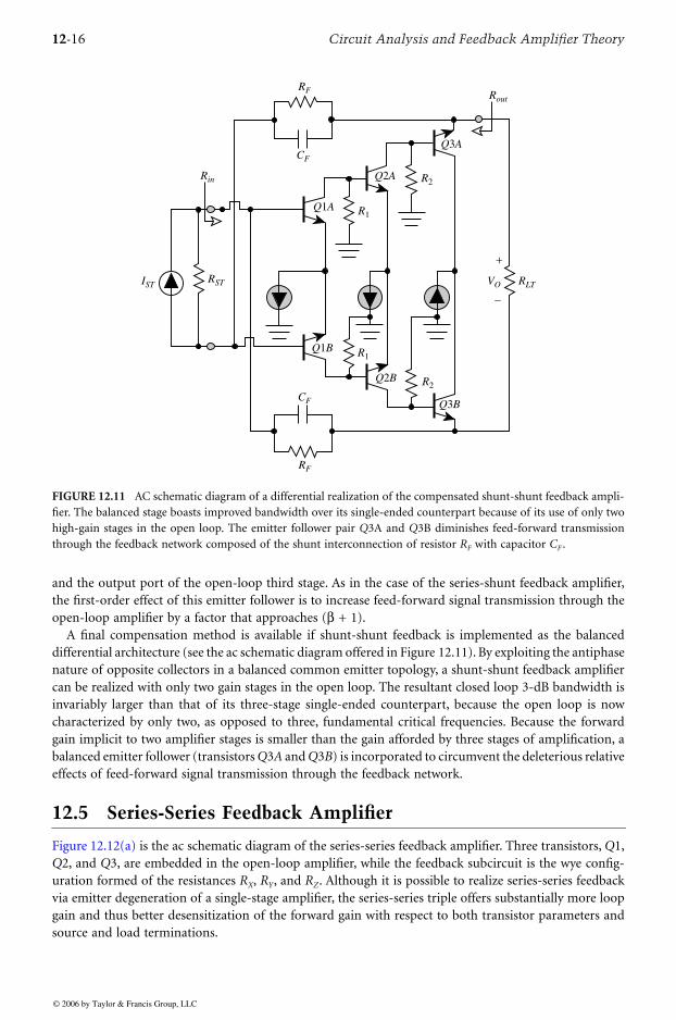
A final compensation method is available if shunt-shunt feedback is implemented as the balanceddifferential architecture (see the ac schematic diagram offered in Figure 12.11). By exploiting the antiphasenature of opposite collectors in a balanced common emitter topology, a shunt-shunt feedback amplifiercan be realized with only two gain stages in the open loop. The resultant closed loop 3-dB bandwidth isinvariably larger than that of its three-stage single-ended counterpart, because the open loop is nowcharacterized by only two, as opposed to three, fundamental critical frequencies. Because the forwardgain implicit to two amplifier stages is smaller than the gain afforded by three stages of amplification, abalanced emitter follower (transistors Q3A and Q3B) is incorporated to circumvent the deleterious relativeeffects of feed-forward signal transmission through the feedback network.
12.5 Series-Series Feedback Amplifier
Figure 12.12(a) is the ac schematic diagram of the series-series feedback amplifier. Three transistors, Q1,Q2, and Q3, are embedded in the open-loop amplifier, while the feedback subcircuit is the wye config-uration formed of the resistances RX, RY, and RZ. Although it is possible to realize series-series feedbackvia emitter degeneration of a single-stage amplifier, the series-series triple offers substantially more loopgain and thus better desensitization of the forward gain with respect to both transistor parameters andsource and load terminations.
FIGURE 12.11 AC schematic diagram of a differential realization of the compensated shunt-shunt feedback ampli-fier. The balanced stage boasts improved bandwidth over its single-ended counterpart because of its use of only twohigh-gain stages in the open loop. The emitter follower pair Q3A and Q3B diminishes feed-forward transmissionthrough the feedback network composed of the shunt interconnection of resistor RF with capacitor CF .
Q2A
Q3A
Q1A
Q1B
Q2B
Q3B
R1
R2
R1
R2
ISTRST RLT
Rout
Rin
RF
CF
VO
CF
RF
−
+
© 2006 by Taylor & Francis Group, LLC

Feedback Amplifier Configurations 12-17
In Figure 12.12(a), the feedback wye senses the Q3 emitter current, which is a factor of (1/α) of theoutput signal current Io. This sampled current is fed back as a voltage in series with the emitter of Q1.Because output current is fed back as a voltage to a voltage-driven input port, both the driving pointinput and output resistances are large. The circuit is therefore best suited as a transconductance amplifierin the sense that for large loop gain, its closed-loop transconductance, GM (RST, RLT) = IO/VST, is almostindependent of the source and load resistances.
The series-series topology of the subject amplifier conduces z-parameter modeling of the feedbacknetwork. Noting the electrical variables delineated in the diagram of Figure 12.12(a),
(12.47)
Equation (12.47) suggests that the open-circuit feedback network resistances loading the emitters oftransistors Q1 and Q3 are (RX + RZ ) and (RY + RZ ), respectively, and the voltage fed back to the emitterof transistor Q1 is RZI2F. Because the indicated feedback network current I2F is (–IO /α), this fed backvoltage is equivalent to (–RZIO /α), which suggests a feedback factor, f, of
FIGURE 12.12 (a) AC schematic diagram of a bipolar series-series feedback amplifier. (b) Low-frequency, small-signal equivalent circuit of the feedback amplifier.
−
+R1 R2
Q1 Q2 Q3Rout
RST
VSTRin
I1F I2F
IV
RX RY
RZV1F V2F
IO
RLT
FEEDBACKNETWORK
(a)
(b)
IV
VST
RSTRin
V2F
V1F
I1F
R2
RLT
K1 β IV (β+1)rib
β IV
IW
βIW
I2F
IO
rbRout
re
rπ
RX +RZ
RY +RZ
f β IV
f IO
− −
−
+
+
+ −
V
V
R R R
R R R
I
I
F
F
X Z Z
Z Y Z
F
F
1
2
1
2
=+
+
© 2006 by Taylor & Francis Group, LLC

12-18 Circuit Analysis and Feedback Amplifier Theory
(12.48)
Finally, the feed-forward through the feedback network if RZ I1F. Because I1F relates to the signal basecurrent IV flowing into transistor Q1 by I1F = (β + 1)Iv, this feed-forward voltage is also expressible as(–f βIv). The foregoing observations and the hybrid-pi method of a bipolar junction transistor producethe small-signal model depicted in Figure 12.12(b). In this model, all transistors are presumed to haveidentical corresponding small-signal parameters, and the constant, K1, is
(12.49)
An analysis of the model of Figure 12.12(b) confirms that the ratio of the signal current, IW, flowinginto the base of transistor Q3 to the signal base current, IV, of transistor Q1 is
(12.50)
This result suggests that feed-forward effects through the feedback network are negligible if � f � � K1R2,which requires
(12.51)
In view of the fact that the constant, K1, approaches β for large values of the resistance, R1, (12.51) is nota troublesome inequality. Introducing a second constant, K2, such that
(12.52)
the ratio IW /IV in (12.50) becomes
(12.53)
assuming (12.51) is satisfied.Given the propriety of (12.50) and using (12.53) the open-loop transconductance, GMO(RST, RLT) is
found to be
(12.54)
and recalling (12.48), the loop gain T is
(12.55)
It follows that for T � 1, the closed-loop transconductance is
(12.56)
fRZ=α
KR
r Rib1
1
11=
+ −( )α
α
I
I
K Rf
K R
r R R RW
V ib Y Z
=+
+ + + −( )
α
α
1 21 2
2
1
1
R K RZ �α 1 2
KR
r R R Rib Y Z2
2
21=
+ + + −( )∆ α
α
I
IK KW
V
≈ 1 2
G R RK K
r R R Rib X ZMO ST LT
ST
,( ) = −+ + + −( )
α
α1 2
1
TR
G R RK K R
r R R RZ Z
ib X Z
= −
( ) =
+ + + −( )α αMO ST LTST
, 1 2
1
G R RG R R
T RMZ
ST LTMO ST LT,
,( ) = ( )+
≈ −1
α
© 2006 by Taylor & Francis Group, LLC

Feedback Amplifier Configurations 12-19
The Early resistance is large enough to justify its neglect, so the open-loop, and thus the closed-loop,driving-point output resistances are infinitely large. On the other hand, the closed-loop driving pointinput resistance Rin can be shown to be
(12.57)
Similar to its shunt-shunt counterpart, the series-series feedback amplifier uses three open-loop gainstages to produce large loop gain. However, also similar to the shunt-shunt triple, frequency compensationvia an introduced feedback zero is difficult unless design care is exercised to realize a dominant poleopen-loop response. To this end, the most commonly used compensation is pole splitting in the openloop, combined, if required, with the introduction of a zero in the feedback factor. The relevant acschematic diagram appears in Figure 12.13 where the indicated capacitance, Cc, inserted across the base-collector terminals of transistor Q3 achieves the aforementioned pole splitting compensation. The capac-itance, CF, in Figure 12.13 delivers a frequency-dependent feedback factor, f (s) of
(12.58)
where the frequency z of the introduced zero derives from
(12.59)
The corresponding pole in (12.58) is insignificant if the closed-loop amplifier is designed for a bandwidth,Bcl that satisfies the inequality, Bc1(RX + RY)CF � 1.
As is the case with shunt-shunt feedback, an alternative frequency compensation scheme is availableif series-series feedback is implemented as a balanced differential architecture. The pertinent ac schematic
FIGURE 12.13 AC schematic diagram of a frequency compensated series-series feedback triple. The capacitance,Cc, achieves pole splitting in the open-loop configuration, while the capacitance, CF, introduces a zero in the feedbackfactor of the closed-loop amplifier.
RX RY
RZ
CF
RLTRST
VST
Rin
Rout
IO
Cc
R1 R2
Q1 Q2 Q3
+
−
R R f G R K K RZin ino MO LT= + ( )[ ] ≈ +( )1 0 1 1 2, β
f s f
s
z
s
z
R
R R RZ
Z X Y
( ) =+
++
1
1
11
zR R
R R
RCX Y
X Y
ZF= +( ) +
© 2006 by Taylor & Francis Group, LLC
12-20 Circuit Analysis and Feedback Amplifier Theory
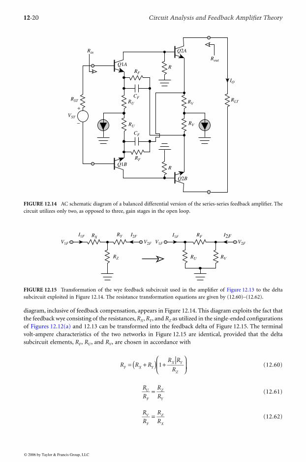
diagram, inclusive of feedback compensation, appears in Figure 12.14. This diagram exploits the fact thatthe feedback wye consisting of the resistances, RX, RY, and RZ as utilized in the single-ended configurationsof Figures 12.12(a) and 12.13 can be transformed into the feedback delta of Figure 12.15. The terminalvolt-ampere characteristics of the two networks in Figure 12.15 are identical, provided that the deltasubcircuit elements, RF, RU, and RV, are chosen in accordance with
(12.60)
(12.61)
(12.62)
FIGURE 12.14 AC schematic diagram of a balanced differential version of the series-series feedback amplifier. Thecircuit utilizes only two, as opposed to three, gain stages in the open loop.
FIGURE 12.15 Transformation of the wye feedback subcircuit used in the amplifier of Figure 12.13 to the deltasubcircuit exploited in Figure 12.14. The resistance transformation equations are given by (12.60)–(12.62).
RLTRV
RV
RU
RU
Rin
Rout
RF
CF
CF
R
RF
R
RST
VST
IO
Q2A
Q1A
Q2B
Q1B
+
−
RXRY
RZ
RF
RU RV
V1F V2FV2F V1F
I1F I1FI2F I2F
R R RR R
RF X YX Y
Z
= +( ) +
1
R
R
R
RU
F
Z
Y
=
R
R
R
RV
F
Z
X
=
© 2006 by Taylor & Francis Group, LLC

Feedback Amplifier Configurations 12-21
12.6 Dual-Loop Feedback
As mentioned previously, a simultaneous control of the driving point I/O resistances, as well as the closed-loop gain, mandates the use of dual global loops comprised of series and shunt feedback signal paths.The two global dual-loop feedback architectures are the series-series/shunt-shunt feedback amplifierand the series-shunt/shunt-series feedback amplifier. In the following subsections, both of these unitsare studied by judiciously applying the relevant analytical results established earlier for pertinent single-loop feedback architectures. The ac schematic diagrams of these respective circuit realizations are pro-vided, and engineering design considerations are offered.
Series-Series/Shunt-Shunt Feedback Amplifier
Figure 12.16 is a behavioral abstraction of the series-series/shunt-shunt feedback amplifier. Two port zparameters are used to model the series-series feedback subcircuit, for which feed-forward is tacitlyignored and the feedback factor associated with its current controlled voltage source is fss. On the otherhand, y parameters model the shunt-shunt feedback network, where the feedback factor relative to itsvoltage controlled current source is fpp. As in the series-series network, feed-forward in the shunt-shuntsubcircuit is presumed negligible. The four-terminal amplifier around which the two feedback units areconnected has an open loop (meaning fss = 0 and fpp = 0, but with the loading effects of both feedbackcircuits considered) transconductance of GMO (RST, RLT).
With fpp set to zero to deactivate shunt-shunt feedback, the resultant series-series feedback network isa transconductance amplifier with a closed-loop transconductance, GMS (RST, RLT), is
(12.63)
where the loop gain, fssGMO (RST, RLT), is presumed much larger than one, and the loading effects of boththe series-series feedback subcircuit and the deactivated shunt-shunt feedback network are incorporated
FIGURE 12.16 System-level diagram of a series-series/shunt-shunt dual-loop feedback amplifier. Note that feed-forward signal transmission through either feedback network is ignored.
G R RI
V
G R R
f G R R fO
ss ssMS ST LT
ST
MO ST LT
MO ST LT
,( , )
,( ) = =
+ ( ) ≈1
1
RLT
RST
VST
VO
IO
fppVO
+
+
+
−
−
−
fss IO
Amplifier
Shunt-Shunt Feedback
Series-Series Feedback
© 2006 by Taylor & Francis Group, LLC

12-22 Circuit Analysis and Feedback Amplifier Theory
into GMO(RST, RLT). The transresistance, RMS(RST, RLT), implied by (12.63), which expedites the study ofthe shunt-shunt component of the feedback configuration, is
(12.64)
The series-series feedback input and output resistances Rins and Routs, respectively, are large and given by
(12.65)
and
(12.66)
where the zero feedback ( fss = 0 and fpp = 0) values, Rino and Routo, of these driving point quantities arecomputed with due consideration given to the loading effects imposed on the amplifier by both feedbacksubcircuits.
When shunt-shunt feedback is applied around the series-series feedback cell, the configurationbecomes a transresistance amplifier. The effective open-loop transresistance is RMS(RST, RLT), as definedby (12.64). Noting a feedback of fpp, the corresponding closed-loop transresistance is
(12.67)
which is independent of amplifier model parameters, despite the unlikely condition of an effective loopgain fpp RST RLT /fss that is much larger than one. It should be interjected, however, that (12.67) presumesnegligible feed-forward through the shunt-shunt feedback network. This presumption may be inappro-priate owing to the relatively low closed-loop gain afforded by the series-series feedback subcircuit.Ignoring this potential problem temporarily, (12.67) suggests a closed-loop voltage gain AV (RST, RLT) of
(12.68)
The closed-loop, driving-point output resistance Rout, can be straightforwardly calculated by notingthat the open circuit (RLT → ∞) voltage gain, AVO, predicted by (12.68) is AVO = 1/fpp RST. Accordingly,(12.68) is alternatively expressible as
(12.69)
Because (12.69) is a voltage divider relationship stemming from a Thévenin model of the output port ofthe dual-loop feedback amplifier, as delineated in Figure 12.17, it follows that the driving-point outputresistance is
(12.70)
R R RV
IR R
I
V
R R
fO O
ssMS ST LT
STST LT
ST
ST LT,( ) = = ≈
R R f G Rssins ino MO LT= + ( )[ ]1 0,
R R f G Rss MO STouts outo= + ( )[ ]1 0,
R R R
R R
f
fR R
f
Mss
ppss
ST LT
ST LT
ST LT
,( ) ≈+
1
A R RV
V
R R R
R
R
f f R RVO
S
M
ss ppST LT
ST LT
ST
LT
ST LT
,,( ) = = ( ) ≈
+
A R R AR
Rf
f R
V VOss
pp
ST LTLT
LTST
,( ) ≈+
Rf
f Rss
ppout
ST
≈
© 2006 by Taylor & Francis Group, LLC

Feedback Amplifier Configurations 12-23
Observe that, similar to the forward gain characteristics, the driving-point output resistance is nominallyinsensitive to changes and other uncertainties in open-loop amplifier parameters. Moreover, this outputresistance is directly proportional to the ratio fss/fpp of feedback factors. As is illustrated in precedingsections, the individual feedback factors, and thus the ratio of feedback factors, is likely to be proportionalto a ratio of resistances. In view of the fact that resistance ratios can be tightly controlled in a monolithicfabrication process, Rout in (12.70) is accurately prescribed for a given source termination.
The driving-point input resistance Rin can be determined from a consideration of the input portcomponent of the system level equivalent circuit depicted in Figure 12.17. This resistance is the ratio ofVST to I, under the condition of RS = 0. With RS = 0, (12.68) yields VO = RLTVST /fss and thus, Kirchhoff ’svoltage law (KVL) applied around the input port of the model at hand yields
(12.71)
where the “open-loop” input resistance Rins, defined by (12.65), is presumed large. Similar to the driving-point output resistance of the series-series/shunt-shunt feedback amplifier, the driving-point input resis-tance is nominally independent of open-loop amplifier parameters.
It is interesting to observe that the input resistance in (12.71) is inversely proportional to the loadresistance by the same factor (fss /fpp) that the driving-point output resistance in (12.70) is inverselyproportional to the source resistance. As a result,
(12.72)
Thus, in addition to being stable performance indices for well-defined source and load terminations, thedriving-point input and output resistances track one another, despite manufacturing uncertainties andchanges in operating temperature that might perturb the individual values of the two feedback factorsfss and fpp.
FIGURE 12.17 Norton equivalent input and Thévenin equivalent output circuits for the series-series/shunt-shuntdual-loop feedback amplifier.
RST
RST
I
VST
VST
RLT
RLTRINS
VO
VO
Rout
Rin
fppVO AVOVS
+
+ +
+
+
−
−−
−
−
Series-Series/Shunt-Shunt
Amplifier
1 3
2 4
1 3
2 4
RR
f R R
f
f
f Rpp
ss
ss
ppin
ins
LT ins LT1+
= ≈
f
fR R R Rss
pp
≈ ≡in LT out ST
© 2006 by Taylor & Francis Group, LLC

12-24 Circuit Analysis and Feedback Amplifier Theory
The circuit property stipulated by (12.72) has immediate utility in the design of wideband commun-ication transceivers and other high-speed signal-processing systems [10–14]. In these and related appli-cations, a cascade of several stages is generally required to satisfy frequency response, distortion, andnoise specifications. A convenient way of implementing a cascade interconnection is to force each memberof the cascade to operate under the match terminated case of RST = Rin = RLT = Rout =
∆ R. From (12.72)match terminated operation demands feedback factors selected so that
(12.73)
which forces a match terminated closed-loop voltage gain A∗V of
(12.74)
The ac schematic diagram of a practical, single-ended series-series/shunt-shunt amplifier is submittedin Figure 12.18. An inspection of this diagram reveals a topology that coalesces the series-series andshunt-shunt triples studied earlier. In particular, the wye network formed of the three resistances, RXx,RY, and RZ, comprises the series-series component of the dual-loop feedback amplifier. The capacitor,Cc, narrowbands the open-loop amplifier to facilitate frequency compensation of the series-series loopthrough the capacitance, CF1. Compensated shunt feedback of the network is achieved by the parallelcombination of the resistance, RF and the capacitance, CF2. If CF1 and Cc combine to deliver a dominantpole series-series feedback amplifier, CF2 is not necessary. Conversely, CF1 is superfluous if CF2 and Cc
interact to provide a dominant pole shunt-shunt feedback amplifier. As in the single ended series-seriesconfiguration, transistor Q3 can be broadbanded via a common base cascode. Moreover, if feedbackthrough the feedback networks poses a problem, an emitter follower can be inserted at the port to whichthe shunt feedback path and the load termination are incident.
FIGURE 12.18 AC schematic diagram of a frequency-compensated, series-series/shunt-shunt, dual-loop feedbackamplifier. The compensation is affected by the capacitances CF1 and CF2, while Cc achieves pole splitting in the open-loop amplifier.
Rf
fss
pp
=
Af R f f
Vpp pp ss
∗ ≈ =1
2
1
2
RLTRST
VST
RX RY
RZ
IO
VO
Rout
RF
Rin
Cc
CF2
R2R1
CF1
Q1 Q2 Q3
+
−
© 2006 by Taylor & Francis Group, LLC

Feedback Amplifier Configurations 12-25
A low-frequency analysis of the circuit in Figure 12.18 is expedited by assuming high beta transistorshaving identical corresponding small-signal model parameters. This analysis, which in contrast to thesimplified behavioral analysis, does not ignore the electrical effects of the aforementioned feed-forwardthrough the shunt-shunt feedback network, yields a voltage gain AV (RST, RLT), of
(12.75)
where the driving-point input resistance of the amplifier Rin is
(12.76)
The driving-point output resistance Rout is
(12.77)
As predicted by the behavioral analysis Rin, Rout, and AV (RST, RLT), are nominally independent of transistorparameters. Observe that the functional dependence of Rin on the load resistance, RLT , is identical to themanner in which Rout is related to the source resistance RST. In particular, Rin ≡ Rout if RST ≡ RLT . For thematch terminated case in which RST = Rin = RLT = Rout =
∆ R,
(12.78)
The corresponding match terminated voltage gain in (12.75) collapses to
(12.79)
Similar to the series-series and shunt-shunt triples, many of the frequency compensation problemsimplicit to the presence of three open-loop stages can be circumvented by realizing the series-series/shunt-shunt amplifier as a two-stage differential configuration. Figure 12.19 is the acschematic diagram of acompensated differential series-series/shunt-shunt feedback dual.
Series-Shunt/Shunt-Series Feedback Amplifier
The only other type of global dual loop architecture is the series-shunt/shunt-series feedback amplifier;the behavioral diagram appears in Figure 12.20. The series-shunt component of this system, which ismodeled by h-parameters, has a negligibly small feed-forward factor and a feedback factor of fsp. Hybridg-parameters model the shunt-series feedback structure, which has a feedback factor of fps and a presum-ably negligible feed-forward factor. The four-terminal amplifier around which the two feedback unitsare connected has an open-loop (meaning fsp = 0 and fps = 0, but with the loading effects of both feedbackcircuits considered) voltage gain of AVO(RST, RLT).
For fps = 0, the series-shunt feedback circuit voltage gain AVS(RST, RLT), is
(12.80)
A R RR
R R
R
R R
R
RVF
F
ZST LT
in
in ST
LT
LT
,( ) ≈ −+
+
−
α1
RR R
R
R
F
Z
inLT
LT
≈ +
+1α
RR R
R
R
F
z
outST
ST
≈ +
+1α
RR RF Z≈
α
AR R
RVF∗ ≈ − −
2
A R RV
V
A R R
f A R R fO
sp spVS ST LT
ST
VO ST LT
VO ST LT
,,
,( ) = = ( )
+ ( ) ≈1
1
© 2006 by Taylor & Francis Group, LLC

12-26 Circuit Analysis and Feedback Amplifier Theory
FIGURE 12.19 AC schematic diagram of the differential realization of a compensated series-series/shunt-shuntfeedback amplifier.
FIGURE 12.20 System level diagram of a series-shunt/shunt-series, dual-loop feedback amplifier. Note that feed-forward signal transmission through either feedback network is ignored.
+
+
−
− RU
RU
RV
RVRST
VST
Rin
RLTVO
IO
RRF1
RF1
RF2
CF2
CF2
RF2
CF1
CF1
RQ1B
Q1A
Q2A
Q2B
Rout
RLT
RST
VST
VO
IO
fps IO
fspVO
Series-Series Feedback
Shunt-Shunt Feedback
Amplifier
+
+
−
− +
−
© 2006 by Taylor & Francis Group, LLC

Feedback Amplifier Configurations 12-27
where the approximation reflects an assumption of a large loop gain. When the shunt-series componentof the feedback amplifier is activated, the dual-loop configuration functions as a current amplifier. Itseffective open-loop transfer function is the current gain, AIS (RST, RLT), established by the series-shuntamplifier; namely,
(12.81)
It follows that the current gain, AI (RST, RLT), of the closed loop is
(12.82)
while the corresponding voltage gain, AV (RST, RLT), assuming negligible feed-forward through the shunt-series feedback network, is
(12.83)
Repeating the analytical strategy employed to determine the input and output resistances of the series-series/shunt-shunt configuration, (12.83) delivers a driving-point input resistance of
(12.84)
and a driving-point output resistance of
(12.85)
Similar to the forward voltage gain, the driving-point input and output resistances of the series-shunt/shunt-series feedback amplifier are nominally independent of active element parameters. Note, how-ever, that the input resistance is directly proportional to the load resistance by a factor (fsp /fps), which is theinverse of the proportionality constant that links the output resistance to the source resistance. Specifically,
(12.86)
Thus, although Rin and Rout are reliably determined for well-defined load and source terminations, theydo not track one another as well as they do in the series-series/shunt-shunt amplifier. Using (12.86), thevoltage gain in (12.83) is expressible as
(12.87)
A R RI
I
R
R
V
V
R
f RO O
spIS ST LT
ST
ST
LT ST
ST
LT
,( ) = =
≈
A R R
R
f R
fR
f R
R
f R f Rsp
pssp
sp psI ST LT
ST
LT
ST
LT
ST
LT ST
,( ) ≈+
=+
1
A R RR
RA R R
R
f R f RV Isp ps
ST LTLT
STST LT
LT
LT ST
, ,( ) = ( ) ≈+
Rf R
fsp
psin
LT≈
Rf R
fps
spout
ST≈
f
f
R
R
R
Rsp
ps
= =in
LT
ST
out
A R R
fR R
R R
V
sp
ST LT
out ST
in LT
,( ) ≈
+
1
1
© 2006 by Taylor & Francis Group, LLC

12-28 Circuit Analysis and Feedback Amplifier Theory
The simplified ac schematic diagram of a practical series-shunt/shunt-series feedback amplifier appearsin Figure 12.21. In this circuit, series-shunt feedback derives from the resistances, REE1 and RF1, and shunt-series feedback is determined by the resistances, REE2 and RF2. Because this circuit topology merges theseries-shunt and shunt-series pairs, requisite frequency compensation, which is not shown in the subjectfigure, mirrors the relevant compensation schemes studied earlier. Note, however, that a cascade of onlytwo open-loop gain stages renders compensation easier to implement and larger 3-dB bandwidths easierto achieve in the series-series/shunt-shunt circuit, which requires three open-loop gain stages for a single-ended application.
For high beta transistors having identical corresponding small-signal model parameters, a low-fre-quency analysis of the circuit in Figure 12.21 gives a voltage gain of
(12.88)
where the driving-point input resistance, Rin, of the subject amplifier is
(12.89)
The driving-point output resistance, Rout, is
(12.90)
FIGURE 12.21 AC schematic diagram of a series-shunt/shunt-series, dual-loop feedback amplifier.
−
+
Rin
RST
VST
RLT
Rout
VO
R
RF2
RF1
REE1 REE2
Q1
Q2
A R RR
R R
R
RVS
ST LTin
in
F1
EE1
,( ) ≈+
+
αα
1
R R
R
RR
R
R
R R
in LT
F2
EE2
F1
EE1
LT
EE1 EE2
≈+
+ +
α1
1
R R
R
RR
R
R
R R
out ST
F1
EE1
F2
EE2
ST
EE1 EE2
≈+
+ +
1
1
© 2006 by Taylor & Francis Group, LLC

Feedback Amplifier Configurations 12-29
12.7 Summary
This section documents small-signal performance equations, general operating characteristics, and engi-neering design guidelines for the six most commonly used global feedback circuits. These observationsderive from analyses based on the judicious application of signal flow theory to the small-signal modelthat results when the subject feedback network is supplanted by an appropriate two-port parameterequivalent circuit.
Four of the six fundamental feedback circuits are single-loop architectures.
1. The series-shunt feedback amplifier functions best as a voltage amplifier in that its input resistanceis large, and its output resistance is small. Because only two gain stages are required in the openloop, the amplifier is relatively easy to compensate for acceptable closed-loop damping and featurespotentially large 3-dB bandwidth. A computationally efficient analysis aimed toward determiningloop gain, closed-loop gain, I/O resistances, and the condition that renders feed-forward throughthe feedback network inconsequential is predicated on replacing the feedback subcircuit with itsh-parameter model.
2. The shunt-series feedback amplifier is a current amplifier in that its input resistance is small, andits output resistance is large. Similar to its series-shunt dual, only two gain stages are required inthe open loop. Computationally efficient analyses are conducted by replacing the feedback sub-circuit with its g-parameter model.
3. The shunt-shunt feedback amplifier is a transresistance signal processor in that both its input andoutput resistances are small. Although this amplifier can be realized theoretically with only a singleopen-loop stage, a sufficiently large loop gain generally requires a cascade of three open-loopstages. As a result, pole splitting is invariably required to ensure an open-loop dominant poleresponse, thereby limiting the achievable closed-loop bandwidth. In addition compensation of thefeedback loop may be required for acceptable closed-loop damping. The bandwidth and stabilityproblems implicit to the use of three open-loop gain stages can be circumvented by a balanceddifferential realization, which requires a cascade of only two open-loop gain stages. Computation-ally efficient analyses are conducted by replacing the feedback subcircuit with its y-parametermodel.
4. The series-series feedback amplifier is a transconductance signal processor in that both its inputand output resistances are large. Similar to its shunt-shunt counterpart, its implementation gen-erally requires a cascade of three open-loop gain stages. Computationally efficient analyses areconducted by replacing the feedback subcircuit with its z-parameter model.
The two remaining feedback circuits are dual-loop topologies that can stabilize the driving-point inputand output resistances, as well as the forward gain characteristics, with respect to shifts in active elementparameters. One of these latter architectures, the series-series/shunt-shunt feedback amplifier, is partic-ularly well suited to electronic applications that require a multistage cascade.
1. The series-series/shunt-shunt feedback amplifier coalesces the series-series architecture with itsshunt-shunt dual. It is particularly well suited to applications, such as wideband communicationnetworks, which require match terminated source and load resistances. Requisite frequency com-pensation and broadbanding criteria mirror those incorporated in the series-series and shunt-shunt single-loop feedback topologies.
2. The series-shunt/shunt-series feedback amplifier coalesces the series-shunt architecture with itsshunt-series dual. Although its input resistance can be designed to match the source resistanceseen by the input port of the amplifier, and its output resistance can be matched to the loadresistance driven by the amplifier, match terminated operating (Rin = RST = RLT = Rout) is notfeasible. Requisite frequency compensation and broadbanding criteria mirror those incorporatedin the series-shunt and shunt-series single-loop feedback topologies.
© 2006 by Taylor & Francis Group, LLC

12-30 Circuit Analysis and Feedback Amplifier Theory
References
[1] J. Millman and A. Grabel, Microelectronics, 2nd ed., New York: McGraw-Hill, 1987, chap. 12.[2] A. B. Grebene, Bipolar and MOS Analog Integrated Circuit Design, New York: Wiley-Interscience,
1984, pp. 424–432.[3] R. G. Meyer, R. Eschenbach, and R. Chin, “A wideband ultralinear amplifier from DC to 300 MHz,”
IEEE J. Solid-State Circuits, vol. SC-9, pp. 167–175, Aug. 1974.[4] A. S. Sedra and K. C. Smith, Microelectronic Circuits, New York: Holt, Rinehart Winston, 1987,
pp. 428–441.[5] J. M. Early, “Effects of space-charge layer widening in junction transistors,” Proc. IRE, vol. 46,
pp. 1141–1152, Nov. 1952.[6] A. J. Cote Jr. and J. B. Oakes, Linear Vacuum-Tube And Transistor Circuits, New York: McGraw-
Hill, 1961, pp. 40–46.[7] R. G. Meyer and R. A. Blauschild, “A four-terminal wideband monolithic amplifier,” IEEE J. Solid-
State Circuits, vol. SC-17, pp. 634–638, Dec. 1981.[8] M. Ohara, Y. Akazawa, N. Ishihara, and S. Konaka, “Bipolar monolithic amplifiers for a gigabit
optical repeater,” IEEE J. Solid-State Circuits, vol. SC-19, pp. 491–497, Aug. 1985.[9] M. J. N. Sibley, R. T. Univin, D. R. Smith, B. A. Boxall, and R. J. Hawkins, “A monolithic transim-
pedance preamplifier for high speed optical receivers,” British Telecommunicat. Tech. J., vol. 2,pp. 64–66, July 1984.
[10] J. F. Kukielka and C. P. Snapp, “Wideband monolithic cascadable feedback amplifiers using siliconbipolar technology,” IEEE Microwave Millimeter-Wave Circuits Symp. Dig., vol. 2, pp. 330, 331, June1982.
[11] R. G. Meyer, M. J. Shensa, and R. Eschenbach, “Cross modulation and intermodulation in amplifiersat high frequencies,” IEEE J. Solid-State Circuits, vol. SC-7, pp. 16–23, Feb. 1972.
[12] K. H. Chan and R. G. Meyer, “A low distortion monolithic wide-band amplifier,” IEEE J. Solid-State Circuits, vol. SC-12, pp. 685–690, Dec. 1977.
[13] A. Arbel, “Multistage transistorized current modules,” IEEE Trans. Circuits Syst., vol. CT-13,pp. 302–310, Sep. 1966.
[14] A. Arbel, Analog Signal Processing and Instrumentation, London: Cambridge University, 1980,chap. 3.
[15] W. G. Beall, “New feedback techniques for high performance monolithic wideband amplifiers,”Electron. Res. Group, University of Southern California, Tech. Memo., Jan. 1990.
© 2006 by Taylor & Francis Group, LLC