Embed Size (px)
DESCRIPTION
Shunt-Shunt Feedback Amplifier - Ideal Case. Feedback circuit does not load down the basic amplifier A, i.e. doesn’t change its characteristics Doesn’t change gain A Doesn’t change pole frequencies of basic amplifier A Doesn’t change R i and R o - PowerPoint PPT Presentation
Citation preview
Ch. 8 Feedback 1ECE 352 Electronics II Winter 2003
* Feedback circuit does not load down the basic amplifier A, i.e. doesn’t change its characteristics
Doesn’t change gain A Doesn’t change pole frequencies of basic
amplifier A Doesn’t change Ri and Ro
* For this configuration, the appropriate gain is the TRANSRESISTANCE GAIN A = ARo = Vo/Ii
* For the feedback amplifier as a whole, feedback changes midband transresistance gain from ARo to ARfo
* Feedback changes input resistance from Ri to Rif
* Feedback changes output resistance from Ro to Rof
* Feedback changes low and high frequency 3dB frequencies
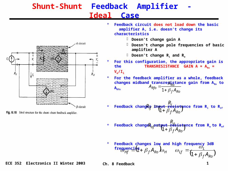
Shunt-Shunt Feedback Amplifier - Ideal Case
Rof
RoRfo A
AA
1
Rof
iif A
RR
1
Rof
oof A
RR
1
Rof
LLfHRofHf A
A
11
Ch. 8 Feedback 2ECE 352 Electronics II Winter 2003
Shunt-Shunt Feedback Amplifier - Ideal Case
Gain
Rof
Ro
i
of
Ro
i
f
Ro
fi
iRo
s
oRfo A
A
I
VA
I
IA
II
IA
I
VA
111
Input Resistance
Rof
i
i
ofi
s
ofi
s
fi
s
s
sif
A
R
I
VI
V
VI
V
II
V
I
VR
11
Output Resistance
Rof
oof
offRooof
offo
of
o
i
ofioff
fis
o
iRoo
o
iRooo
o
oof
A
RRso
RARR
RI
V
I
I
VIsoVIand
IIsoIBut
I
IAR
I
IARI
I
VR
1
'
'
'
''
0
''
'
'
'Io’
Vo’+_
Is = 0
Ch. 8 Feedback 3ECE 352 Electronics II Winter 2003
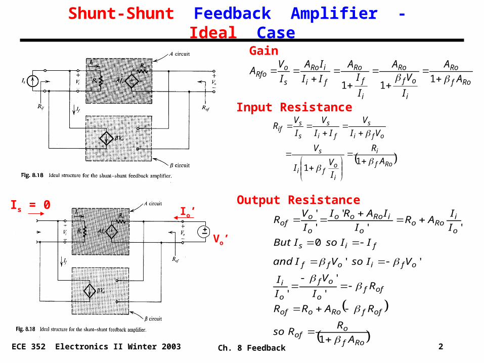
* Feedback network is a two port network (input and output ports)
* Can represent with Y-parameter network (This is the best for this feedback amplifier configuration)
* Y-parameter equivalent network has FOUR parameters
* Y-parameters relate input and output currents and voltages
* Two parameters chosen as independent variables. For Y-parameter network, these are input and output voltages V1 and V2
* Two equations relate other two quantities (input and output currents I1 and I2) to these independent variables
* Knowing V1 and V2, can calculate I1 and I2 if you know the Y-parameter values
* Y-parameters have units of conductance (1/ohms=siemens) !
Equivalent Network for Feedback Network
Ch. 8 Feedback 4ECE 352 Electronics II Winter 2003
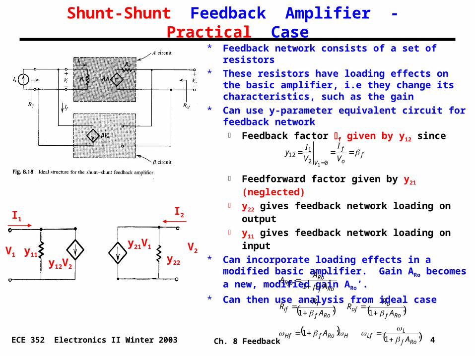
* Feedback network consists of a set of resistors
* These resistors have loading effects on the basic amplifier, i.e they change its characteristics, such as the gain
* Can use y-parameter equivalent circuit for feedback network
Feedback factor f given by y12 since
Feedforward factor given by y21 (neglected)
y22 gives feedback network loading on output
y11 gives feedback network loading on input
* Can incorporate loading effects in a modified basic amplifier. Gain ARo becomes a new, modified gain ARo’.
* Can then use analysis from ideal case
Shunt-Shunt Feedback Amplifier - Practical Case
fo
f
VV
I
V
Iy
02
112
1
'1
'1
'1'1
'1
'
Rof
LLfHRofHf
Rof
oof
Rof
iif
Rof
RoRfo
AA
A
RR
A
RR
A
AA
y22
y21V1y11
y12V2
V1V2
I1I2
Ch. 8 Feedback 5ECE 352 Electronics II Winter 2003
Shunt-Shunt Feedback Amplifier - Practical Case
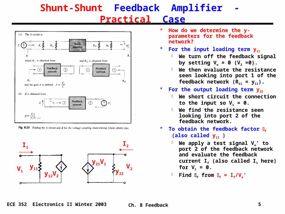
* How do we determine the y-parameters for the feedback network?
* For the input loading term y11 We turn off the feedback signal by
setting Vo = 0 (V2 =0). We then evaluate the resistance
seen looking into port 1 of the feedback network (R11 = y11).
* For the output loading term y22
We short circuit the connection to the input so V1 = 0.
We find the resistance seen looking into port 2 of the feedback network.
* To obtain the feedback factor f (also called y12 )
We apply a test signal Vo’ to port 2 of the feedback network and evaluate the feedback current If (also called I1 here) for V1 = 0.
Find f from f = If/Vo’
y22
y21V1y11
y12V2
I1I2
V1V2
Ch. 8 Feedback 6ECE 352 Electronics II Winter 2003
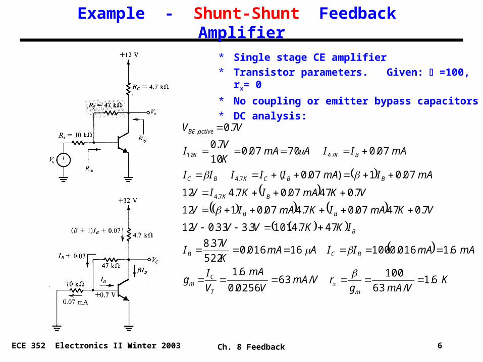
* Single stage CE amplifier
* Transistor parameters. Given: =100, rx= 0
* No coupling or emitter bypass capacitors
* DC analysis:
Example - Shunt-Shunt Feedback Amplifier
KVmAg
rVmAV
mA
V
Ig
mAmAIIAmAK
VI
IKKVVV
VKmAIKmAIV
VKmAIKIV
mAImAIIIII
mAIIAmAK
VI
VV
mT
Cm
BCB
B
BB
BK
BBCKBC
BKK
activeBE
6.1/63
100/63
0256.0
6.1
6.1016.010016016.0522
37.8
477.41013.333.012
7.04707.07.407.0112
7.04707.07.412
07.01)07.0(
07.07007.010
7.0
7.0
7.4
7.4
4710
,
Ch. 8 Feedback 7ECE 352 Electronics II Winter 2003
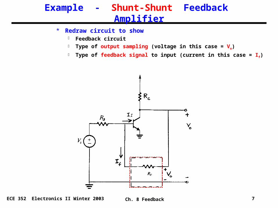
* Redraw circuit to show Feedback circuit Type of output sampling (voltage in this case = Vo)
Type of feedback signal to input (current in this case = If)
Example - Shunt-Shunt Feedback Amplifier
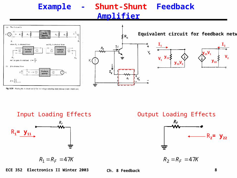
Ch. 8 Feedback 8ECE 352 Electronics II Winter 2003
Example - Shunt-Shunt Feedback Amplifier
Input Loading Effects Output Loading Effects
KRR F 471
R1= y11 R2= y22
KRR F 472
y22
y21V1y11
y12V2
I1
V1V2
I2
Equivalent circuit for feedback network
Ch. 8 Feedback 9ECE 352 Electronics II Winter 2003
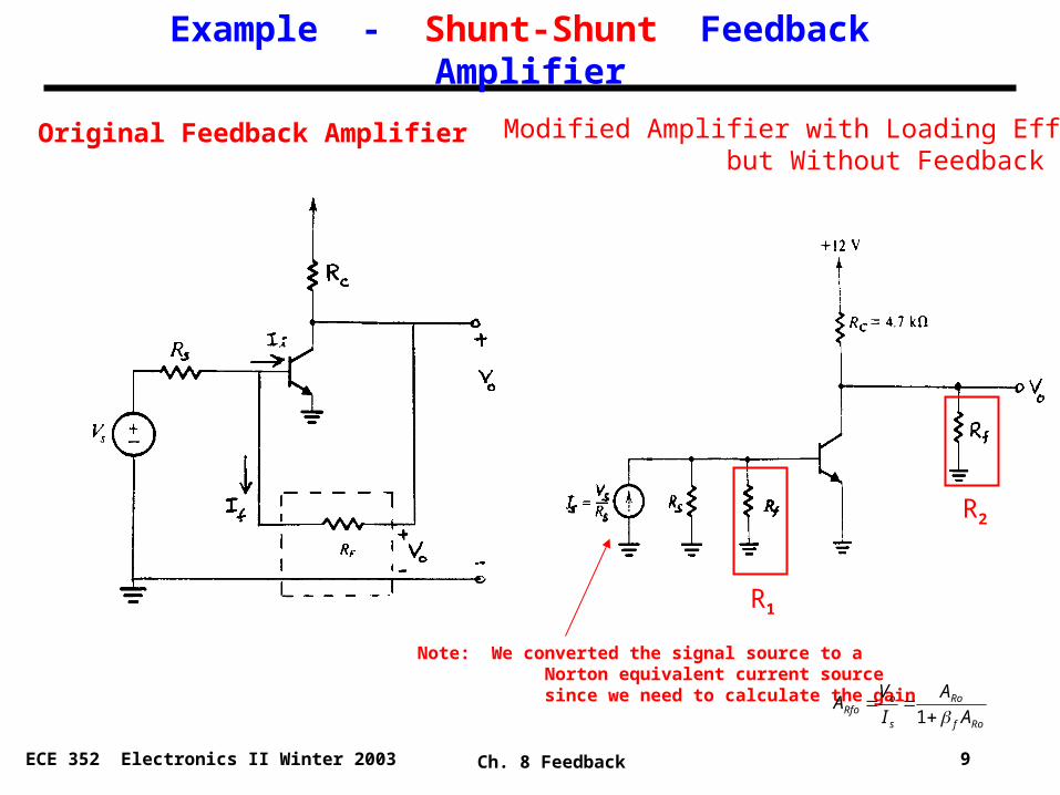
Example - Shunt-Shunt Feedback Amplifier
Modified Amplifier with Loading Effects, but Without Feedback
Note: We converted the signal source to a Norton equivalent current source since we need to calculate the gain
Original Feedback Amplifier
R1
R2
Rof
Ro
s
oRfo A
A
I
VA
1
Ch. 8 Feedback 10ECE 352 Electronics II Winter 2003
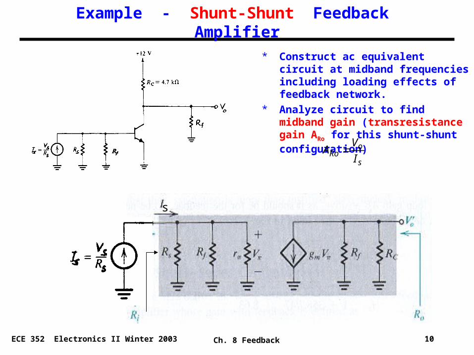
* Construct ac equivalent circuit at midband frequencies including loading effects of feedback network.
* Analyze circuit to find midband gain (transresistance gain ARo for this shunt-shunt configuration)
Example - Shunt-Shunt Feedback Amplifier
s
oRo I
VA
s
Ch. 8 Feedback 11ECE 352 Electronics II Winter 2003
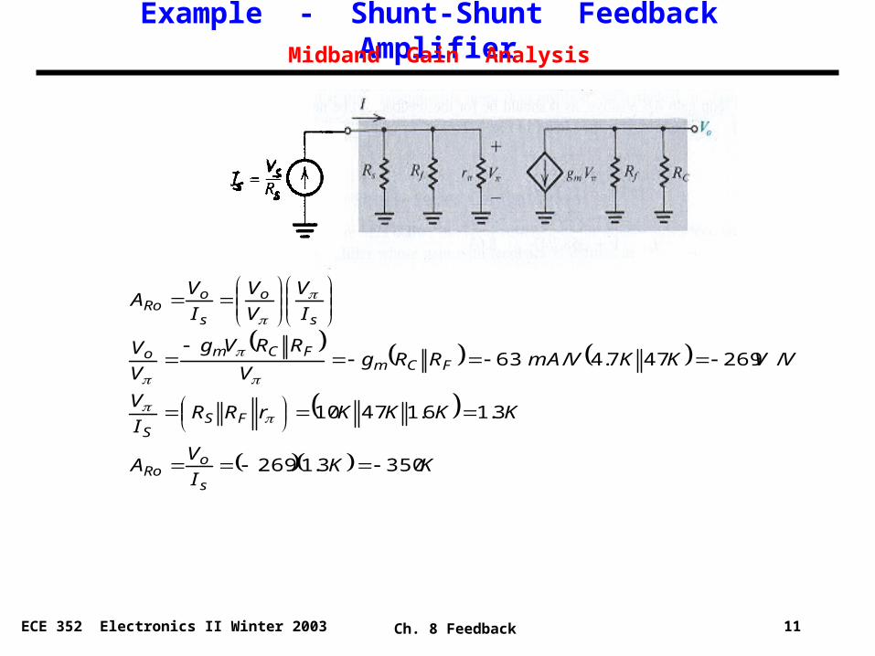
Example - Shunt-Shunt Feedback AmplifierMidband Gain Analysis
KK
I
VA
KKKKrRRI
V
VVKKVmARRgV
RRVg
V
V
I
V
V
V
I
VA
s
oRo
FSS
FCmFCmo
s
o
s
oRo
3503.1269
3.16.14710
/269477.4/63
Ch. 8 Feedback 12ECE 352 Electronics II Winter 2003
Midband Gain with Feedback
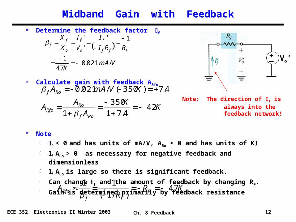
* Determine the feedback factor f
* Calculate gain with feedback ARfo
* Note f < 0 and has units of mA/V, ARo < 0 and has units of K f ACo > 0 as necessary for negative feedback and dimensionless
f ACo is large so there is significant feedback.
Can change f and the amount of feedback by changing RF.
Gain is determined primarily by feedback resistance
VmA
K
RRI
I
V
I
X
X
Fff
f
o
f
o
ff
/021.047
1
1'
'
'
KK
A
AA
KVmAA
Rof
RoRfo
Rof
424.71
350
1
4.7)350(/021.0
KRR
A FFf
Rfo 47)/1(
11
+_ Vo’
Note: The direction of If is always into the feedback network!
Ch. 8 Feedback 13ECE 352 Electronics II Winter 2003
Input and Output Resistances with Feedback
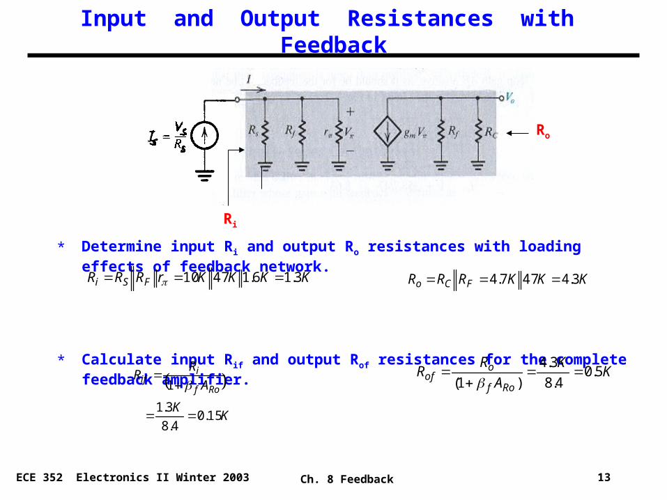
* Determine input Ri and output Ro resistances with loading effects of feedback network.
* Calculate input Rif and output Rof resistances for the complete feedback amplifier.
KKKKrRRR FSi 3.16.14710
K
K
A
RR
Rof
iif
15.04.8
3.1
1
KKKRRR FCo 3.4477.4
KK
A
RR
Rof
oof 5.0
4.8
3.4
)1(
Ri
Ro
Ch. 8 Feedback 14ECE 352 Electronics II Winter 2003
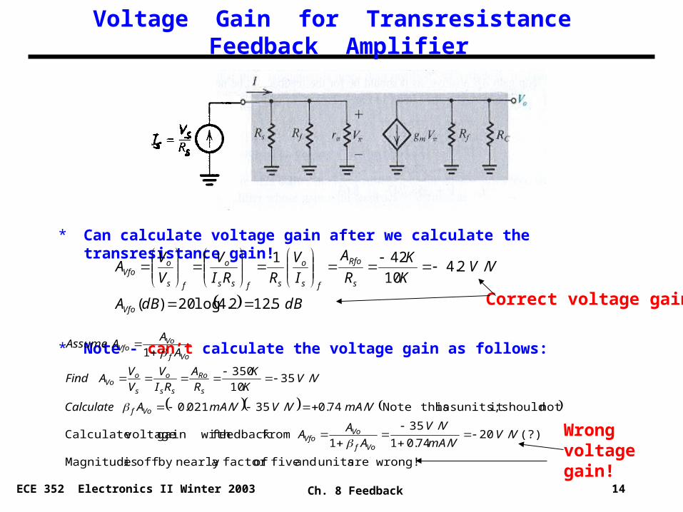
Voltage Gain for Transresistance Feedback Amplifier
* Can calculate voltage gain after we calculate the transresistance gain!
* Note - can’t calculate the voltage gain as follows: dBdBA
VVK
K
R
A
I
V
RRI
V
V
VA
Vfo
s
Rfo
fs
o
sfss
o
fs
oVfo
5.122.4log20)(
/2.410
421
wrong!are units and five offactor anearly by off is Magnitude
(?)/20/74.01
/35
1 fromfeedback gain with voltageCalculate
not! shouldit units; has thisNote/74.0/35/021.0
/3510
350
1
VVVmA
VV
A
AA
VmAVVVmAACalculate
VVK
K
R
A
RI
V
V
VAFind
A
AAAssume
Vof
VoVfo
Vof
s
Ro
ss
o
s
oVo
Vof
VoVfo
Correct voltage gain
Wrongvoltage gain!
Ch. 8 Feedback 15ECE 352 Electronics II Winter 2003
Equivalent Circuit for Shunt-Shunt Feedback Amplifier
* Transresistance gain amplifier A = Vo/Is
* Feedback modified gain, input and output resistances
Included loading effects of feedback network
Included feedback effects of feedback network
* Significant feedback, i.e. f
ARo is large and positive
KA
A
I
VA
Rof
Ro
fS
oRfo 42
1
VVR
AA
KA
AA
KVmAA
S
RfoVfo
fRof
RoRfo
Rof
/2.4
471
1
4.7)350(/021.0
KK
A
RR
Rof
iif 15.0
4.8
3.1
1
KK
A
RR
Rof
oof 5.0
4.8
3.4
)1(
Rif ARfoI i
Rof
Ch. 8 Feedback 16ECE 352 Electronics II Winter 2003
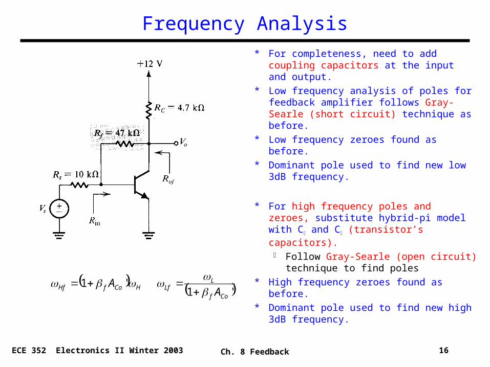
Frequency Analysis
* For completeness, need to add coupling capacitors at the input and output.
* Low frequency analysis of poles for feedback amplifier follows Gray-Searle (short circuit) technique as before.
* Low frequency zeroes found as before.
* Dominant pole used to find new low 3dB frequency.
* For high frequency poles and zeroes, substitute hybrid-pi model with C and C (transistor’s capacitors). Follow Gray-Searle (open circuit)
technique to find poles
* High frequency zeroes found as before.
* Dominant pole used to find new high 3dB frequency.
'1'1
Cof
LLfHCofHf A
A