Embed Size (px)
Citation preview

eSimAn open source EDA tool for circuit design,
simulation, analysis and PCB design
eSim User Manualversion 2.1
Prepared By:eSim Team
FOSSEE at IIT, Bombay
Indian Institute of Technology Bombay
BY:© $\© =©August 2020
i

Contents
1 Introduction 2
2 Architecture of eSim 42.1 Modules used in eSim . . . . . . . . . . . . . . . . . . . . . . . . . . . . 4
2.1.1 Eeschema . . . . . . . . . . . . . . . . . . . . . . . . . . . . . . . 42.1.2 CvPcb . . . . . . . . . . . . . . . . . . . . . . . . . . . . . . . . . 52.1.3 Pcbnew . . . . . . . . . . . . . . . . . . . . . . . . . . . . . . . . 52.1.4 KiCad to Ngspice converter . . . . . . . . . . . . . . . . . . . . . 62.1.5 Model Builder . . . . . . . . . . . . . . . . . . . . . . . . . . . . 72.1.6 Subcircuit Builder . . . . . . . . . . . . . . . . . . . . . . . . . . 72.1.7 Ngspice . . . . . . . . . . . . . . . . . . . . . . . . . . . . . . . . 72.1.8 NGHDL . . . . . . . . . . . . . . . . . . . . . . . . . . . . . . . . 72.1.9 OpenModelica . . . . . . . . . . . . . . . . . . . . . . . . . . . . 7
2.2 Work flow of eSim . . . . . . . . . . . . . . . . . . . . . . . . . . . . . . 7
3 Installing eSim 103.1 eSim installation in Ubuntu OS . . . . . . . . . . . . . . . . . . . . . . . 103.2 eSim installation in Windows OS . . . . . . . . . . . . . . . . . . . . . . 10
4 Getting Started 114.1 How to launch eSim? . . . . . . . . . . . . . . . . . . . . . . . . . . . . . 114.2 eSim User Interface . . . . . . . . . . . . . . . . . . . . . . . . . . . . . . 12
4.2.1 Menubar . . . . . . . . . . . . . . . . . . . . . . . . . . . . . . . 134.2.2 Toolbar . . . . . . . . . . . . . . . . . . . . . . . . . . . . . . . . 134.2.3 Project Explorer . . . . . . . . . . . . . . . . . . . . . . . . . . . 174.2.4 Dockarea . . . . . . . . . . . . . . . . . . . . . . . . . . . . . . . 174.2.5 Console Area . . . . . . . . . . . . . . . . . . . . . . . . . . . . . 18
5 Schematic Creation 195.1 Familiarizing the Schematic Editor interface . . . . . . . . . . . . . . . . 19
5.1.1 Top menu bar . . . . . . . . . . . . . . . . . . . . . . . . . . . . . 19

5.1.2 Top toolbar . . . . . . . . . . . . . . . . . . . . . . . . . . . . . . 215.1.3 Toolbar on the right . . . . . . . . . . . . . . . . . . . . . . . . . 225.1.4 Toolbar on the left . . . . . . . . . . . . . . . . . . . . . . . . . . 235.1.5 Hotkeys . . . . . . . . . . . . . . . . . . . . . . . . . . . . . . . . 23
5.2 eSim component libraries . . . . . . . . . . . . . . . . . . . . . . . . . . 245.3 Schematic creation for simulation . . . . . . . . . . . . . . . . . . . . . . 25
5.3.1 Selection and placement of components . . . . . . . . . . . . . . 255.3.2 Wiring the circuit . . . . . . . . . . . . . . . . . . . . . . . . . . 275.3.3 Assigning values to components . . . . . . . . . . . . . . . . . . . 285.3.4 Annotation and ERC . . . . . . . . . . . . . . . . . . . . . . . . 285.3.5 Netlist generation . . . . . . . . . . . . . . . . . . . . . . . . . . 28
5.4 Tools for creating the PCB layout . . . . . . . . . . . . . . . . . . . . . 295.4.1 FootPrint Editor . . . . . . . . . . . . . . . . . . . . . . . . . . . 305.4.2 PCB Layout . . . . . . . . . . . . . . . . . . . . . . . . . . . . . 30
6 Simulation 316.1 Kicad to Ngspice Conversion . . . . . . . . . . . . . . . . . . . . . . . . 31
6.1.1 Analysis . . . . . . . . . . . . . . . . . . . . . . . . . . . . . . . . 316.1.2 Source Details . . . . . . . . . . . . . . . . . . . . . . . . . . . . 326.1.3 Ngspice Model . . . . . . . . . . . . . . . . . . . . . . . . . . . . 326.1.4 Device Modelling . . . . . . . . . . . . . . . . . . . . . . . . . . . 336.1.5 Sub Circuit . . . . . . . . . . . . . . . . . . . . . . . . . . . . . . 34
6.2 Simulating the schematic . . . . . . . . . . . . . . . . . . . . . . . . . . 346.2.1 Simulation . . . . . . . . . . . . . . . . . . . . . . . . . . . . . . 346.2.2 Multimeter . . . . . . . . . . . . . . . . . . . . . . . . . . . . . . 36
7 Model Editor 387.1 Creating New Model Library . . . . . . . . . . . . . . . . . . . . . . . . 387.2 Editing Current Model Library . . . . . . . . . . . . . . . . . . . . . . . 407.3 Uploading external .lib file to eSim repository . . . . . . . . . . . . . . . 41
8 SubCircuit Builder 428.1 Creating a SubCircuit . . . . . . . . . . . . . . . . . . . . . . . . . . . . 428.2 Edit a Subcircuit . . . . . . . . . . . . . . . . . . . . . . . . . . . . . . . 478.3 Upload subcircuit . . . . . . . . . . . . . . . . . . . . . . . . . . . . . . . 48
9 NGHDL-Mixed Signal Simulation 499.1 Introduction . . . . . . . . . . . . . . . . . . . . . . . . . . . . . . . . . . 499.2 Digital Model creation using NGHDL . . . . . . . . . . . . . . . . . . . 519.3 Schematic Creation . . . . . . . . . . . . . . . . . . . . . . . . . . . . . . 52
iii

10 OpenModelica 6110.1 Introduction . . . . . . . . . . . . . . . . . . . . . . . . . . . . . . . . . . 61
10.1.1 OMEdit . . . . . . . . . . . . . . . . . . . . . . . . . . . . . . . . 6110.1.2 OMOptim . . . . . . . . . . . . . . . . . . . . . . . . . . . . . . . 61
10.2 OpenModelica in eSim . . . . . . . . . . . . . . . . . . . . . . . . . . . . 6210.2.1 OM Optimisation . . . . . . . . . . . . . . . . . . . . . . . . . . . 63
11 Solved Examples 6911.1 Solved Examples . . . . . . . . . . . . . . . . . . . . . . . . . . . . . . . 69
11.1.1 Basic RC Circuit . . . . . . . . . . . . . . . . . . . . . . . . . . . 6911.1.2 Half Wave Rectifier . . . . . . . . . . . . . . . . . . . . . . . . . . 7611.1.3 Inverting Amplifier . . . . . . . . . . . . . . . . . . . . . . . . . . 7911.1.4 Half Adder . . . . . . . . . . . . . . . . . . . . . . . . . . . . . . 8311.1.5 Full Wave Rectifier using SCR . . . . . . . . . . . . . . . . . . . 8611.1.6 Oscillator Circuit . . . . . . . . . . . . . . . . . . . . . . . . . . . 9011.1.7 Characteristics of BJT in Common Base Configuration . . . . . . 93
12 PCB Design 9712.1 Schematic creation for PCB design . . . . . . . . . . . . . . . . . . . . . 97
12.1.1 Removing components required for simulation from the schematic 9712.1.2 Mapping of components using Cvpcb . . . . . . . . . . . . . . . . 9812.1.3 Familiarising with Cvpcb Window . . . . . . . . . . . . . . . . . 9812.1.4 Viewing footprints in 2D and 3D . . . . . . . . . . . . . . . . . . 10012.1.5 Mapping of components in the circuit . . . . . . . . . . . . . . . 10012.1.6 Netlist generation for PCB . . . . . . . . . . . . . . . . . . . . . 102
12.2 Creation of PCB layout . . . . . . . . . . . . . . . . . . . . . . . . . . . 10312.2.1 Launching Pcbnew . . . . . . . . . . . . . . . . . . . . . . . . . . 10312.2.2 Familiarizing the Layout Editor tool . . . . . . . . . . . . . . . . 10312.2.3 Hotkeys . . . . . . . . . . . . . . . . . . . . . . . . . . . . . . . . 10412.2.4 Designing PCB layout for 7805VoltageRegulator circuit . . . . . 105
13 Appendix 11413.1 Appendix A . . . . . . . . . . . . . . . . . . . . . . . . . . . . . . . . . . 114
13.1.1 Backing up important data before uninstalling eSim . . . . . . . 11413.1.2 Uninstalling eSim . . . . . . . . . . . . . . . . . . . . . . . . . . . 114
13.2 Appendix B . . . . . . . . . . . . . . . . . . . . . . . . . . . . . . . . . . 11513.2.1 Pin types in KiCad . . . . . . . . . . . . . . . . . . . . . . . . . . 11513.2.2 ERC Table . . . . . . . . . . . . . . . . . . . . . . . . . . . . . . 115
13.3 Appendix C . . . . . . . . . . . . . . . . . . . . . . . . . . . . . . . . . . 11613.3.1 Shortcut keys in Schematic editor . . . . . . . . . . . . . . . . . 11613.3.2 Shortcut keys in PCB editor . . . . . . . . . . . . . . . . . . . . 117
iv

13.4 Appendix D: ERC errors . . . . . . . . . . . . . . . . . . . . . . . . . . . 11713.5 Appendix E: Checks to be done before Simulation in NGHDL . . . . . . 11913.6 Appendix F: Common Errors in NGHDL . . . . . . . . . . . . . . . . . 121
13.6.1 NGHDL Upload Errors . . . . . . . . . . . . . . . . . . . . . . . 12113.6.2 Simulation Related Errors . . . . . . . . . . . . . . . . . . . . . . 12113.6.3 Model Deletion . . . . . . . . . . . . . . . . . . . . . . . . . . . . 123
13.7 Appendix G: References . . . . . . . . . . . . . . . . . . . . . . . . . . . 124
v

Acknowledgement
There have been many people contributing towards the software development and/or theelectronic system design and simulation for eSim. The following people have contributedin some way.
Development:
• Fahim Khan
• Rahul Paknikar
• Saurabh Bansode
• Gloria Nandihal
• Athul George
• Gaurav Supal
• Kayva Manohar
• Komal Sheth
• Ashutosh Jha
• Sumanto Kar
• Shubhangi Mahajan
• Vadissa Yamini
• Bladen Martin
• Aamir Thekiya
• Neel Manilal Shah
• Padigepati Mallikar-juna Reddy
• Bhargav Katakam
• Anjali Jaiswal
• Mahfooz Ahmad
• Mudit Joshi
• Ashutosh Gangwar
• Akshay NH
• Athul MS
• Powai Labs Technol-ogy Private Limited
Technical Guidance
• Kannan M. Moudgalya
• Pramod Murali
• Madhav P. Desai
• Usha Vishwanathan
• Rupak Rokade
• Sunil Shetye
Financial Sponsorship:
• NMEICT, MHRD, Govt. Of India
• MHRD, Govt. Of India
• Indian Institute of Technology, Bom-bay
If someone helped in the development/simulation and has not been inserted in thislist, then this omission was unintentional. If you feel you should be on this list thenplease write to [email protected]. Do not be shy, we would like to make this listas complete as possible.
1

Chapter 1
Introduction
Electronic systems are an integral part of human life. They have simplified our livesto a great extent. Starting from small systems made of a few discrete components tothe present day integrated circuits (ICs) with millions of logic gates, electronic systemshave undergone a sea change. As a result, design of electronic systems too have becomeextremely difficult and time consuming. Thanks to a host of computer aided designtools, we have been able to come up with quick and efficient designs. These are calledElectronic Design Automation or EDA tools.
Let us see the steps involved in EDA. In the first stage, the specifications of thesystem are laid out. These specifications are then converted to a design. The designcould be in the form of a circuit schematic, logical description using an HDL language,etc. The design is then simulated and re-designed, if needed, to achieve the desiredresults. Once simulation achieves the specifications, the design is either converted toa PCB, a chip layout, or ported to an FPGA. The final product is again tested forspecifications. The whole cycle is repeated until desired results are obtained
A person who builds an electronic system has to first design the circuit, produce avirtual representation of it through a schematic for easy comprehension, simulate it andfinally convert it into a Printed Circuit Board (PCB). There are various tools availablethat will help us do this. Some of the popular EDA tools are those of Cadence, Synopys,Mentor Graphics and Xilinx. Although these are fairly comprehensive and high end,their licenses are expensive, being proprietary.
There are some free and open source EDA tools like gEDA, KiCad and Ngspice. Themain drawback of these open source tools is that they are not comprehensive. Someof them are capable of PCB design (e.g. KiCad) while some of them are capable ofperforming simulations (e.g. gEDA). To the best of our knowledge, there is no opensource software that can perform circuit design, simulation and layout design together.eSim is capable of doing all of the above.
eSim is a free and open source EDA tool. It is an acronym for Electronics Simulation.eSim is created using open source software packages, such as KiCad, Ngspice and

Python. Using eSim, one can create circuit schematics, perform simulations and designPCB layouts. It can create or edit new device models, and create or edit subcircuits forsimulation.
Because of these reasons, eSim is expected to be useful for students, teachers andother professionals who would want to study and/or design electronic systems. eSim isalso useful for entrepreneurs and small scale enterprises who do not have the capabilityto invest in heavily priced proprietary tools.
This book introduces eSim to the reader and illustrates all the features of eSim withexamples. The software architecture of eSim is presented in Chapter 2 while Chapter 3gives the user step by step instructions to install eSim on a typical computer system.Chapter 4 gets the user started with eSim. It takes them through a tour of eSimwith the help of a simple RC circuit example. Chapter 5 illustrates how to create thecircuit schematic in esim and Chapter 6 explains simulating the circuit schematic. Theadvanced features of eSim such as Model Builder and Sub circuit Builder are coveredin Chapter 7 and Chapter 8 respectively. Additional features in eSim like mixed modesimulation and OpenModelica are covered in Chapter 9 and Chapter 10 respectively.Chapter 11 illustrates how to use eSim for solving circuit simulation problems. The lastchapter, Chapter 12 explains how eSim can be used to do PCB layout.
The following convention has been adopted throughout this manual.All the menunames, options under each menu item, tool names, certain points to be noted, etc.,are given in italics. Some keywords, names of certain windows/dialog boxes, names ofsome files/projects/folders, messages displayed during an activity, names of websites,component references, etc., are given in typewriter font. Some key presses, e.g. Enterkey, F1 key, y for yes, etc., are also mentioned in typewriter font.
3
Chapter 2
Architecture of eSim
eSim is a CAD tool that helps electronic system designers to design, test and analysetheir circuits. But the important feature of this tool is that it is open source and hencethe user can modify the source as per his/her need. The software provides a generic,modular and extensible platform for experiment with electronic circuits. This softwareruns on Ubuntu Linux distributions 14.04,16.04, 18.04 and some flavours of Windows.It uses Python 3, KiCad 4.0.7, GHDL and Ngspice.
The objective behind the development of eSim is to provide an open source EDAsolution for electronics and electrical engineers. The software should be capable ofperforming schematic creation, PCB design and circuit simulation (analog, digital andmixed-signal). It should provide facilities to create new models and components. Thearchitecture of eSim has been designed by keeping these objectives in mind.
2.1 Modules used in eSim
Various open-source tools have been used for the underlying build-up of eSim. In thissection we will give a brief idea about all the modules used in eSim.
2.1.1 Eeschema
Eeschema is an integrated software where all functions of circuit drawing, control, layout,library management and access to the PCB design software are carried out. It is theschematic editor tool used in KiCad. Eeschema is intended to work with PCB layoutsoftware such as Pcbnew. It provides netlist that describes the electrical connectionsof the PCB. Eeschema also integrates a component editor which allows the creation,editing and visualization of components. It also allows the user to effectively handlethe symbol libraries i.e; import, export, addition and deletion of library components.Eeschema also integrates the following additional but essential functions needed for a

modern schematic capture software:1. Design rules check (DRC) for the automatic control of incorrect connections and
inputs of components left unconnected. 2. Generation of layout files in POSTSCRIPT orHPGL format. 3. Generation of layout files printable via printer. 4. Bill of materialsgeneration. 5. Netlist generation for PCB layout or for simulation.
This module is indicated by the label 1 in Fig. 2.1.As Eeschema is originally intended for PCB Design, there are no fictitious com-
ponents1 such as voltage or current sources. Thus, we have added a new library fordifferent types of voltage and current sources such as sine, pulse and square wave. Wehave also built a library which gives printing and plotting solutions. This extension,developed by us for eSim, is indicated by the label 2 in Fig. 2.1.
2.1.2 CvPcb
CvPcb is a tool that allows the user to associate components in the schematic to compo-nent footprints when designing the printed circuit board. CvPcb is the footprint editortool in KiCad. Typically the netlist file generated by Eeschema does not specify whichprinted circuit board footprint is associated with each component in the schematic.However, this is not always the case as component footprints can be associated dur-ing schematic capture by setting the component’s footprint field. CvPcb provides aconvenient method of associating footprints to components. It provides footprint listfiltering, footprint viewing, and 3D component model viewing to help ensure that thecorrect footprint is associated with each component. Components can be assigned totheir corresponding footprints manually or automatically by creating equivalence files.Equivalence files are look up tables associating each component with its footprint. Thisinteractive approach is simpler and less error prone than directly associating footprintsin the schematic editor. This is because CvPcb not only allows automatic association,but also allows to see the list of available footprints and displays them on the screen toensure the correct footprint is being associated. This module is indicated by the label3 in Fig. 2.1.
2.1.3 Pcbnew
Pcbnew is a powerful printed circuit board software tool. It is the layout editor toolused in KiCad. It is used in association with the schematic capture software Eeschema,which provides the netlist. Netlist describes the electrical connections of the circuit.CvPcb is used to assign each component, in the netlist produced by Eeschema, to amodule that is used by Pcbnew. The features of Pcbnew are given below:
1Signal generator or power supply is not a single component but in circuit simulation, we considerthem as a component. While working with actual circuit, signal generator or power supply gives inputto the circuit externally thus, doesn’t require for PCB design.
5

• It manages libraries of modules. Each module is a drawing of the physical com-ponent including its footprint - the layout of pads providing connections to thecomponent. The required modules are automatically loaded during the reading ofthe netlist produced by CvPcb.
• Pcbnew integrates automatically and immediately any circuit modification by re-moval of any erroneous tracks, addition of new components, or by modifying anyvalue (and under certain conditions any reference) of old or new modules, accord-ing to the electrical connections appearing in the schematic.
• This tool provides a rats nest display, a hairline connecting the pads of modulesconnected on the schematic. These connections move dynamically as track andmodule movements are made.
• It has an active Design Rules Check (DRC) which automatically indicates any errorof track layout in real time.
• It automatically generates a copper plane, with or without thermal breaks on thepads.
• It has a simple but effective auto router to assist in the production of the circuit.An export/import in SPECCTRA dsn format allows to use more advanced auto-routers.
• It provides options specifically for the production of ultra high frequency circuits(such as pads of trapezoidal and complex form, automatic layout of coils on theprinted circuit).
• Pcbnew displays the elements (tracks, pads, texts, drawings and more) as actualsize and according to personal preferences such as:
– display in full or outline.
– display the track/pad clearance.
This module is indicated by the label 4 in Fig. 2.1.
2.1.4 KiCad to Ngspice converter
Analysis parameters, and the source details are provided through this module. It alsoallows us to add and edit the device models and subcircuits, included in the circuitschematic. Finally, this module facilitates the conversion of KiCad netlist to Ngspicecompatible ones.It is developed by us for eSim and it is indicated by the label 7 in Fig. 2.1. The use ofthis module is explained in detail in section (yet to be put).
6

2.1.5 Model Builder
This tool provides the facility to define a new model for devices such as, 1. Diode2. Bipolar Junction Transistor (BJT) 3. Metal Oxide Semiconductor Field Effect Tran-sistor (MOSFET) 4. Junction Field Effect Transistor (JFET) 5. IGBT and 6. Magneticcore. This module also helps edit existing models. It is developed by us for eSim and itis indicated by the label 5 in Fig. 2.1.
2.1.6 Subcircuit Builder
This module allows the user to create a subcircuit for a component. Once the subcircuitfor a component is created, the user can use it in other circuits. It has the facility todefine new components such as, Op-amps, IC-555, UJT and so on. This componentalso helps edit existing subcircuits. This module is developed by us for eSim and it isindicated by the label 6 in Fig. 2.1.
2.1.7 Ngspice
Ngspice is a general purpose circuit simulation program for nonlinear dc, nonlineartransient, and linear ac analysis. Circuits may contain resistors, capacitors, inductors,mutual inductors, independent voltage and current sources, four types of dependentsources, lossless and lossy transmission lines (two separate implementations), switches,uniform distributed RC lines, and the five most common semiconductor devices: diodes,BJTs, JFETs, MESFETs, and MOSFET. This module is indicated by the label 9 inFig. 2.1.
2.1.8 NGHDL
NGHDL, a module for mixed mode circuit simulation is also integrated with eSim.It uses ghdl for digital simulation and the mixed mode simulation happens throughNgSpice.
2.1.9 OpenModelica
OpenModelica (OM) is an open source modeling and simulation tool based on Modelicalanguage. Two modules of OpenModelica, OMEdit, an IDE for modeling and simulationand OMOptim, an IDE for optimisation are integrated with eSim.
2.2 Work flow of eSim
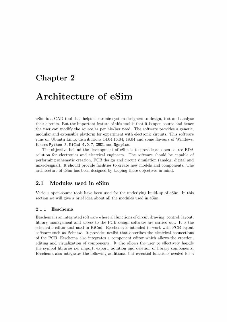
Fig. 2.1 shows the work flow in eSim. The block diagram consists of mainly three parts:
• Schematic Editor
7
Figure 2.1: Work flow in eSim. (Boxes with dotted lines denote the modules developedin this work).
• PCB Layout Editor
• Circuit Simulators
Here we explain the role of each block in designing electronic systems. Circuit designis the first step in the design of an electronic circuit. Generally a circuit diagram is drawnon a paper, and then entered into a computer using a schematic editor. Eeschema isthe schematic editor for eSim. Thus all the functionalities of Eeschema are naturallyavailable in eSim.
Libraries for components, explicitly or implicitly supported by Ngspice, have beencreated using the features of Eeschema. As Eeschema is originally intended for PCBdesign, there are no fictitious components such as voltage or current sources. Thus, anew library for different types of voltage and current sources such as sine, pulse andsquare wave, has been added in eSim. A library which gives the functionality of printingand plotting has also been created.
The schematic editor provides a netlist file, which describes the electrical connectionsof the design. In order to create a PCB layout, physical components are required to bemapped into their footprints. To perform component to footprint mapping, CvPcb isused. Footprints have been created for the components in the newly created libraries.Pcbnew is used to draw a PCB layout.
8

After designing a circuit, it is essential to check the integrity of the circuit design.In the case of large electronic circuits, breadboard testing is impractical. In such cases,electronic system designers rely heavily on simulation. The accuracy of the simulationresults can be increased by accurate modeling of the circuit elements. Model Builderprovides the facility to define a new model for devices and edit existing models. Complexcircuit elements can be created by hierarchical modeling. Subcircuit Builder providesan easy way to create a subcircuit.
The netlist generated by Schematic Editor cannot be directly used for simulation dueto compatibility issues. Netlist Converter converts it into Ngspice compatible format.The type of simulation to be performed and the corresponding options are providedthrough a graphical user interface (GUI). This is called KiCad to Ngspice Converter ineSim.
eSim uses Ngspice for analog, digital, mixed-level/mixed-signal circuit simulation.Ngspice is based on three open source software packages
• Spice3f5 (analog circuit simulator)
• Cider1b1 (couples Spice3f5 circuit simulator to DSIM device simulator)
• Xspice (code modeling support and simulation of digital components through anevent driven algorithm)
It is a part of gEDA project. Ngspice is capable of simulating devices with BSIM, EKV,HICUM, HiSim, PSP, and PTM models. It is widely used due to its accuracy even forthe latest technology devices.
9
Chapter 3
Installing eSim
3.1 eSim installation in Ubuntu OS
1. Download eSim installer for Linux from http://esim.fossee.in/downloads toa local directory and unpack it. You can also unpack the installer through theterminal. Open the terminal and navigate to the directory where this INSTALLfile is located. Use the following command to unpack:$ unzip eSim-2.1.zip
2. To install eSim and other dependencies run the following command:$ cd eSim-2.1
$ chmod +x install-eSim.sh
$ ./install-eSim.sh --install
3. To run eSim from the terminal, type:$ esim
or you can double click on eSim icon created on the Desktop after installation.
3.2 eSim installation in Windows OS
1. Download eSim-2.1 install.exe from https://esim.fossee.in/downloads
2. Disable the antivirus (if any). Now, double click on the exe file to start theinstallation process. If a window appears, click Yes to complete the installation.
3. By default eSim will be installed in C drive, under an auto-generated FOSSEEFolder. Note that installation directory can neither be in ”Program Files” norcontain spaces in its path.
4. eSim icon will be created on desktop. You can double click on the eSim iconcreated on the Desktop after installation.

Chapter 4
Getting Started
In this chapter we will get started with eSim. Referring to this chapter will make onefamiliar with eSim and will help plan the project before actually designing a circuit.
4.1 How to launch eSim?
After the installation of eSim, a shortcut to eSim is created on the Desktop. To launcheSim double click on the shortcut.Alternately, for Ubuntu Linux users, one can also launch eSim from the terminal.1. Go to terminal.2. Type esim and press Enter.
The first window that appears is the workspace dialog as shown in Fig. 4.1.
Figure 4.1: eSim-Workspace
1.The default workspace is eSim-Workspace under home directory. To select a newworkspace location, use the browse option. Do not select a location which has a space
character or special character(s).
2. If you select the set default click-box, then the chosen location will be set as defaultworkspace and the dialog box won’t appear next time you launch eSim.
3. If you wish to change the default workspace location, then use the menu-bar fromeSim’s main Interface, which is explained in upcoming section.
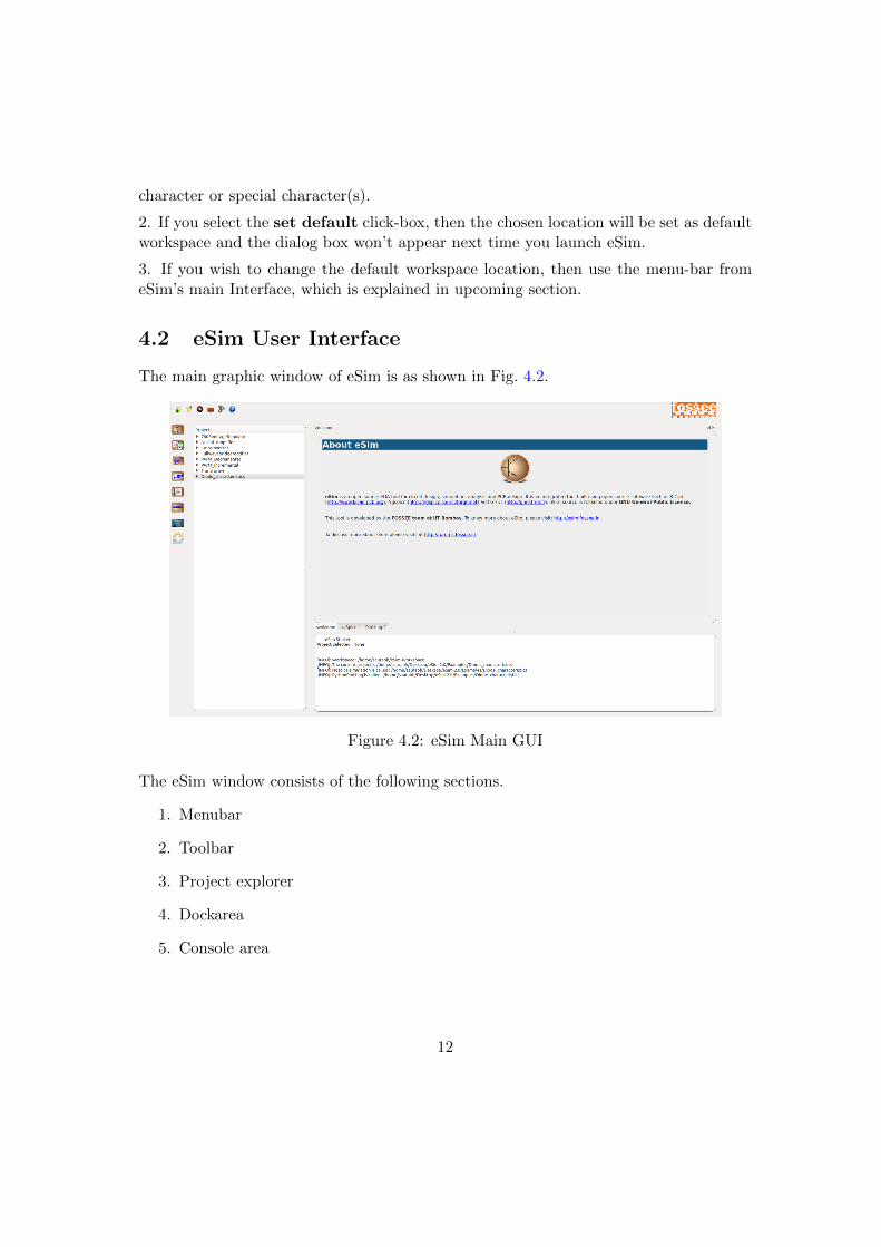
4.2 eSim User Interface
The main graphic window of eSim is as shown in Fig. 4.2.
Figure 4.2: eSim Main GUI
The eSim window consists of the following sections.
1. Menubar
2. Toolbar
3. Project explorer
4. Dockarea
5. Console area
12

4.2.1 Menubar
• New Project: New projects are created in the eSim-Workspace. When this menuis selected, a new window opens up with Enter Project name field. Type thename of the new project and click on OK. A project directory will be created ineSim-Workspace. The name of this folder will be the same as that of the projectcreated. Make sure that the project name does not have any spaces in between.This project is also added to the project explorer.
• Open Project: This opens the file dialog of default eSim-Workspace where theprojects are stored. Select the required project and click on Open. The selectedproject is added to the project explorer.
• Close Project: This button closes the opened project.
• Change workspace : Clicking on this will open the window shown in Fig. 4.1.If you have chosen a default workspace location but wish to change it later on,launch eSim, click on this icon and do the necessary changes.
• Mode Switch : Using this feature user can decide whether to fetch latest foot-prints(refer Section :PCB Designing) from the internet or use the locally availablefootprints.Note : By switching to online mode, you will require a stable and high-speedinternet connection, if it is not available to you then please always remain in theoffline mode.
• Help : Clicking on this icon will launch the eSim user manual for that particularversion of eSim.
4.2.2 Toolbar
The toolbar consists of the following buttons. See Fig. 4.3.
Open Schematic
The first button on the toolbar is the Schematic Editor. Clicking on this button willopen the schematic editor. If a new project is being created, one will get a dialogbox confirming the creation of a schematic. This is illustrated in See Fig. 4.4. How-ever, if an already existing project is opened, the schematic editor window is opened.To know how to use the schematic editor to create circuit schematics, refer to Chapter 5.
When one right clicks on a particular project : three options appear, their functionslisted below:
13
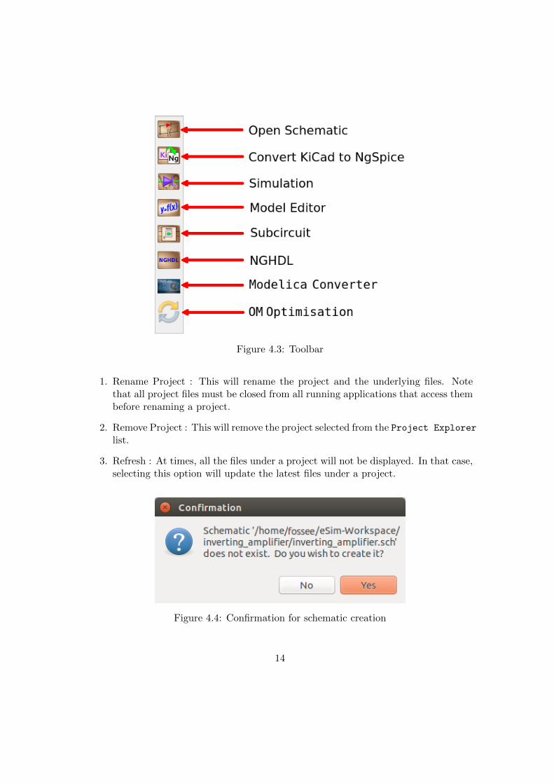
Figure 4.3: Toolbar
1. Rename Project : This will rename the project and the underlying files. Notethat all project files must be closed from all running applications that access thembefore renaming a project.
2. Remove Project : This will remove the project selected from the Project Explorer
list.
3. Refresh : At times, all the files under a project will not be displayed. In that case,selecting this option will update the latest files under a project.
Figure 4.4: Confirmation for schematic creation
14

Convert KiCad to Ngspice
In the schematic editor window, after creating the schematic a netlist is to be generatedwhich contains information about the components present in the schematic created andtheir values specified . Although this netlist is present, it cannot be directly fed to thesimulator. Here the KiCad-to-Ngspice converter comes into play. This tool convertsthe netlist generated from the schematic into another netlist which is compatible withNgspice, the simulator used in eSim. The Convert KiCad to Ngspice window consistsof five tabs namely Analysis, Source Details, Ngspice Model, Device Modeling
and Subcircuits. The details of these tabs are as follows.
• Analysis: This feature helps the user to enter the parameters for performingdifferent types of analysis such as Operating point analysis, DC analysis, ACanalysis, transient analysis, DC Sweep Analysis.
It has the facility to select the
– Type of analysis and
– The simulation parameter values for analysis
• Source Details:eSim sources are added from eSim Sources library in the schematic.Sources such as SINE, AC, DC, PULSE, PWL are in this library. The parametervalues to all the sources added in the schematic can be given through ’SourceDetails’ tab in the KiCad-To-Ngspice window.
• Ngspice Model:Ngspice has in-built model such as basic logic gates, flip-flops,
gain, summer, buffer, DAC and ADC blocketc. which can be utilised whilebuilding a circuit. eSim allows to add and modify Ngspice model parameterthrough Ngspice Model tab.
• Device Modeling:Devices like Diode, JFET, MOSFET, IGBT, MOS etc used inthe circuit can be modeled using device model libraries. eSim also provides editingand adding new model libraries. While converting KiCad to Ngspice, these libraryfiles are added to the corresponding devices used in the circuit.
• Subcircuits:eSim allows you to build subcircuits. The subcircuits can againhave components having subcircuits and so on. This enables users to build com-monly used circuits as subcircuits and then use it across circuits. The subcircuitsare added to the main circuits using this facility. We can also edit already existingsubcircuits.Once the values have been entered, press the Convert button. This will gener-ate the .cir.out file in the same project directory. Note that KiCad to NgspiceConverter can only be used if the KiCad spice netlist .cir file is already generated.
15
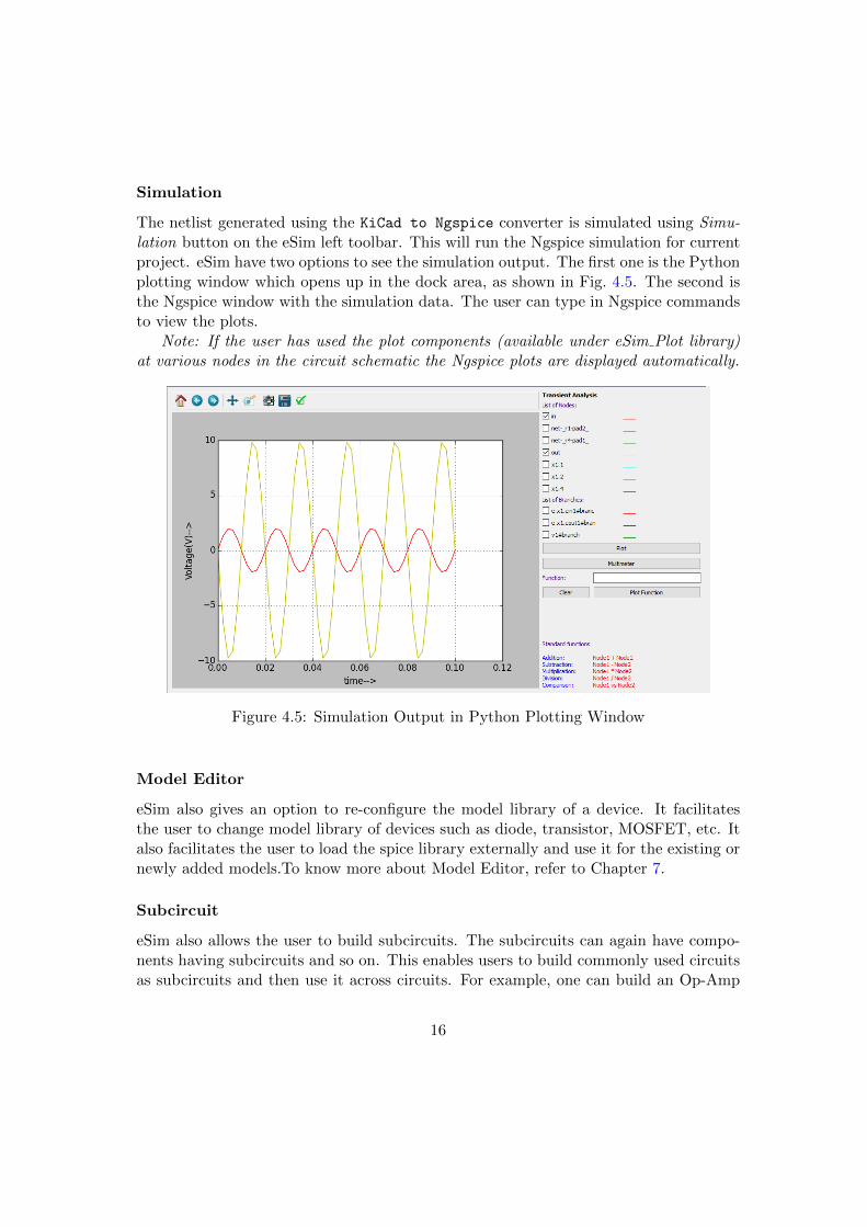
Simulation
The netlist generated using the KiCad to Ngspice converter is simulated using Simu-lation button on the eSim left toolbar. This will run the Ngspice simulation for currentproject. eSim have two options to see the simulation output. The first one is the Pythonplotting window which opens up in the dock area, as shown in Fig. 4.5. The second isthe Ngspice window with the simulation data. The user can type in Ngspice commandsto view the plots.
Note: If the user has used the plot components (available under eSim Plot library)at various nodes in the circuit schematic the Ngspice plots are displayed automatically.
Figure 4.5: Simulation Output in Python Plotting Window
Model Editor
eSim also gives an option to re-configure the model library of a device. It facilitatesthe user to change model library of devices such as diode, transistor, MOSFET, etc. Italso facilitates the user to load the spice library externally and use it for the existing ornewly added models.To know more about Model Editor, refer to Chapter 7.
Subcircuit
eSim also allows the user to build subcircuits. The subcircuits can again have compo-nents having subcircuits and so on. This enables users to build commonly used circuitsas subcircuits and then use it across circuits. For example, one can build an Op-Amp
16

as a subcircuit and then use it as just a single component across circuits without havingto recreate it. Clicking on Subcircuit Builder tool will allow one to edit or create asubcircuit. To know how to make a subcircuit, refer to Chapter 8.
NGHDL
NGHDL is an add on to eSim for mixed mode circuit simulation. By using the foreignlanguage interface of GHDL, NGHDL communicates with Ngspice and accomplishesmixed-mode simulation. Using NGHDL, user can create custom digital model usingVHDL language. From simple multiplexers, counters to microcontrollers and ASICs,any custom component in the digital domain can be realized using the NGHDL tool.The created digital model can be used in either mixed-mode circuit or a standalonecircuit operating in digital domain. NGHDL gives user the liberty to edit existingmodels supplied with eSim per their needs, either for experimenting new ideas or tochange the model per their specific requirement.
Modelica Converter
OpenModelica (OM) is an open source modeling and simulation tool based on Modelicalanguage. Modelica is an object oriented language. The Modelica Converter in eSiminterface, converts the ngspice netlist to Modelica format. This facility will be onlyavailable if you have OpenModelica already installed in the system. More details onhow to use this module is available in Chapter 10.
OM Optimisation
OMOptimisation (OMOptim) is a powerful and interactive tool for performing designoptimisation. It has a good library of electrical components called Modelica StandardLibrary (MSL). OMOptim is stable and robust. It is very easy to add objective functionsto the OMOptim interface.
4.2.3 Project Explorer
Project explorer contains the list of all the projects previously added to it. Select aproject and double click on it, this will display all the files under this project. Rightclick on any displayed file to open it. To remove or refresh any project file from theproject explorer, right click on the main project file.
4.2.4 Dockarea
This area is used to open the following windows.
1. KiCad to Ngspice converter
17

2. Ngspice plotting
3. Python plotting
4. Model builder
5. Subcircuit builder
Modules/Windows will appear here as per your selection.
4.2.5 Console Area
Console area provides the log information about the activity done during the currentsession.
18

Chapter 5
Schematic Creation
The first step in the design of an electronic system is the design of its circuit. Thiscircuit is usually created using a Schematic Editor and is called a Schematic. eSimuses Eeschema as its schematic editor. Eeschema is the schematic editor of KiCad.It is a powerful schematic editor software. It allows the creation and modification ofcomponents and symbol libraries and supports multiple hierarchical layers of printedcircuit design.
5.1 Familiarizing the Schematic Editor interface
Fig. 5.1 shows the schematic editor and the various menu and toolbars. We will explainthem briefly in this section.
5.1.1 Top menu bar
The top menu bar will be available at the top left corner. Some of the important menuoptions in the top menu bar are:
1. File - The file menu items are given below:(a) New - Clear current schematic and start a new one(b) Open - Open a schematic(c) Open Recent - A list of recently opened files for loading(d) Save Schematic project - Save current sheet and all its hierarchy.(e) Save Current Sheet Only - Save current sheet, but not others in a hierarchy.(f) Save Current sheet as - Save current sheet with a new name.(g) Page Settings - Set preferences for printing the page.(h) Print - Access to print menu (See Fig. 5.2).(i) Plot - Plot the schematic in Postscript, HPGL, SVF or DXF format(j) Close - Close the schematic editor.

Figure 5.1: Schematic editor with the menu bar and toolbars marked
Figure 5.2: Print options
2. Place - The place menu has shortcuts for placing various items like components,wire and junction, on to the schematic editor window. See Sec. 5.1.5 to knowmore about various shortcut keys (hotkeys).
3. Preferences - The preferences menu has the following options:
20
(a) Component Libraries - Select component libraries and library paths. Thisenables the user to add the libraries, if the libraries are not loaded in theEeschema.
(b) Schematic Editor Options - Select colors for various items, display optionsand set hot keys.
(c) Language - Shows the current list of available languages. Use default.(d) Import and Export - Contain options to load and save preferences and im-
port/ export hot key configuration files. See Sec. 5.1.5 to know about varioushotkeys.
5.1.2 Top toolbar
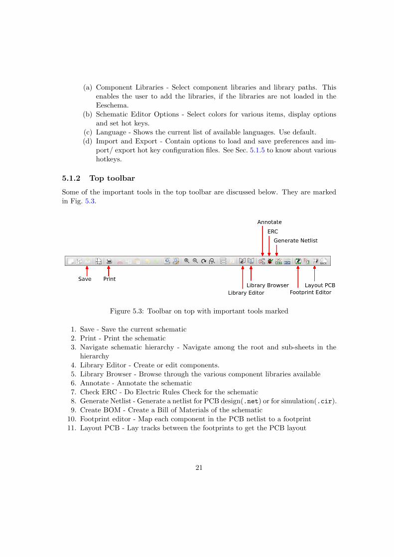
Some of the important tools in the top toolbar are discussed below. They are markedin Fig. 5.3.
Figure 5.3: Toolbar on top with important tools marked
1. Save - Save the current schematic2. Print - Print the schematic3. Navigate schematic hierarchy - Navigate among the root and sub-sheets in the
hierarchy4. Library Editor - Create or edit components.5. Library Browser - Browse through the various component libraries available6. Annotate - Annotate the schematic7. Check ERC - Do Electric Rules Check for the schematic8. Generate Netlist - Generate a netlist for PCB design(.net) or for simulation(.cir).9. Create BOM - Create a Bill of Materials of the schematic
10. Footprint editor - Map each component in the PCB netlist to a footprint11. Layout PCB - Lay tracks between the footprints to get the PCB layout
21
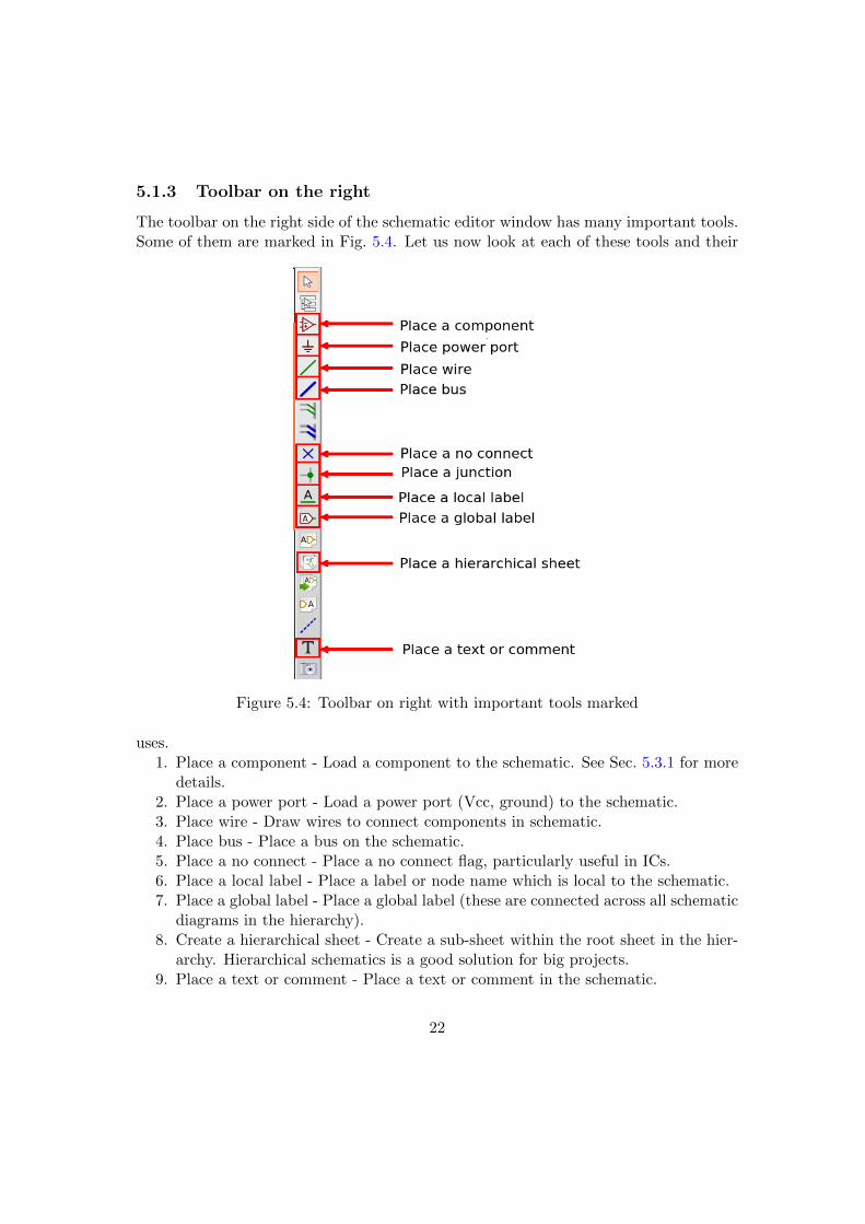
5.1.3 Toolbar on the right
The toolbar on the right side of the schematic editor window has many important tools.Some of them are marked in Fig. 5.4. Let us now look at each of these tools and their
Figure 5.4: Toolbar on right with important tools marked
uses.1. Place a component - Load a component to the schematic. See Sec. 5.3.1 for more
details.2. Place a power port - Load a power port (Vcc, ground) to the schematic.3. Place wire - Draw wires to connect components in schematic.4. Place bus - Place a bus on the schematic.5. Place a no connect - Place a no connect flag, particularly useful in ICs.6. Place a local label - Place a label or node name which is local to the schematic.7. Place a global label - Place a global label (these are connected across all schematic
diagrams in the hierarchy).8. Create a hierarchical sheet - Create a sub-sheet within the root sheet in the hier-
archy. Hierarchical schematics is a good solution for big projects.9. Place a text or comment - Place a text or comment in the schematic.
22

5.1.4 Toolbar on the left
Some of the important tools in the toolbar on the left are discussed below. They aremarked in Fig. 5.5.
Figure 5.5: Toolbar on left with important tools marked
1. Show/Hide grid - Show or Hide the grid in the schematic editor. Pressing the toolagain hides (shows) the grid if it was shown (hidden) earlier.
2. Show hidden pins - Show hidden pins of certain components, for example, powerpins of certain ICs.
5.1.5 Hotkeys
A set of keyboard keys are associated with various operations in the schematic editor.These keys save time and make it easy to switch from one operation to another. Thelist of hotkeys can be viewed by going to Preferences in the top menu bar. ChooseSchematic Editor Options and select Controls tab. The hotkeys can also be editedhere. Some frequently used hotkeys, along with their functions, are given below:• F1 - Zoom in• F2 - Zoom out• Ctrl + Z - Undo• Delete - Delete item• M - Move item• C - Copy item• A - Add/place component• P - Place power component• R - Rotate item• X - Mirror component about X axis• Y - Mirror component about Y axis• E - Edit schematic component• W - Place wire• T - Add text• S - Add sheet
23

Note: Both lower and upper-case keys will work as hotkeys.
5.2 eSim component libraries
eSim schematic editor has a huge collection of components. As Eeschema is meantto be a schematic editor to create circuits for PCB, Eeschema lacks some componentsthat are necessary for simulation (e.g. probes(plot v and current sources). A set ofcomponent libraries has been created with such components under the label eSim *.These libraries are Ngspice compatible. If one is using eSim only for designing a PCB,then one might not need these libraries. However, these libraries are essential if one needsto simulate one’s circuit. Hereafter, we will refer to these libraries as eSim libraries todistinguish them from libraries already present in Eeschema (Eeschema libraries) asshown in Fig. 5.6.
Figure 5.6: eSim-Components Libraries
The following list shows the various eSim component libraries.• eSim Analog - Contains Ngspice analog models such as aswitch(analog switch),
summer(adder model), Transfo(Transformer), zener.• eSim Devices - Includes elementary components like resistor, capacitor, transistor,
MosFet.• eSim Digital - Includes Ngspice digital models such as basic gates (AND, OR,
NOR,NAND,XOR), filpflops (SR, D, JK), buffer, inverter.
24

• eSim Hybrid - Includes components like ADC and DAC.• eSim Miscellaneous - Contains components like ic(used for giving initial conditions
in circuit) and port(used in creating subcircuits).• eSim Plot - Contains plotting components like plot v1 (plot voltage at a node),
plot v2 (plot voltage between 2 nodes), plot i2 (plot current through branch),plot log (plot logarithmic voltage at a node).• eSim Power - Includes power components like DIAC, TRIAC and SCR.• eSim Sources - Contains sources for the circuits like AC voltage source, DC voltage
source, sine source and pulse source.• eSim Subckt - Contains subcircuit components like Op-Amp(UA 741), IC 555,
Half adder and full adder.• eSim User - A repository for all user created components
5.3 Schematic creation for simulation
There are certain differences between the schematic created for simulation and thatcreated for PCB design. We need certain components like plots and current sources forsimulation whereas these are not needed for PCB design. For PCB design, we wouldrequire connectors (e.g. DB15 and 2 pin connector) for taking signals in and out ofthe PCB whereas these have no meaning in simulation. This section covers schematiccreation for simulation. Refer to Chapter 12 to know how to create schematic for PCBdesign.
The first step in the creation of circuit schematic is the selection and placementof required components. Let us see this using an example. Let us create the circuitschematic of an RC filter given in Fig. 5.10c and do a transient simulation.
5.3.1 Selection and placement of components
We would need a resistor, a capacitor, a voltage source, ground terminal and some plotcomponents. To place a resistor on the schematic editor window, select the Place acomponent tool from the toolbar on the right side and click anywhere on the schematiceditor. This opens up the component selection window. This action can also be per-formed by pressing the key A. Choose the eSim Devices library and click on the arrownear it. This will open the eSim Devices library and the resistor component can befound here. Fig. 5.7 shows the selection of resistor component. Click on OK. A resistorwill be tied to the cursor. Place the resistor on the schematic editor by a single click.To place the next component, i.e., capacitor, click again on the schematic editor. Thecapacitor component is also found under eSim Devices library. Select it and then clickon OK. Place the capacitor on the schematic editor by a single click.
Let us now place a sinusoidal voltage source. This is required for performing transientanalysis. On the component selection window, choose the library eSim source. Select
25

Figure 5.7: Placing a resistor using the Place a Component tool
the component SINE and click on OK. Place the sine source on the schematic editor bya single click. Similarly select and place gnd, a ground terminal from the power library.
The plot components can be found under the eSim Plot library. Select the plot v1component and place the component. Once all the components are placed, the schematiceditor would look like as in Fig. 5.8.
Figure 5.8: All RC circuit components placed
Let us rotate the resistor to complete the circuit. To rotate the resistor, place the
26

cursor on the resistor as shown in Fig. 5.9 and press the key R. This applies to allcomponents.
Figure 5.9: Placing the cursor (cross mark) on the resistor component
If one wants to move a component, place the cursor on top of the component andpress the key M. The component will be tied to the cursor and can be moved in anydirection.
5.3.2 Wiring the circuit
The next step is to wire the connections. Let us connect the resistor to the capacitor.To do so, point the cursor to the terminal of resistor to be connected and press the key W.It has now changed to the wiring mode. Alternately, this can also be done by selectingthe Place wire tool on the right side toolbar. Move the cursor towards the terminal ofthe capacitor and click on it. A wire is formed as shown in Fig. 5.10a. Similarly connect
(a) Initial stages (b) Wiring done (c) Final schematic withPWR FLAG
Figure 5.10: Various stages of wiring
the wires between all terminals and the final schematic would look like Fig. 5.10b.
27

5.3.3 Assigning values to components
We need to assign values to the components in our circuit i.e., resistor and capacitor.Note that the sine voltage source has been placed for simulation. The specifications ofsine source will be given during simulation. To assign value to the resistor, place thecursor above the letter R (not R?) and press the key E. Choose Field value. Type 1k inthe Edit value field box as shown in Fig. 5.11. 1k means 1kΩ. Similarly give the value1u for the capacitor. 1u means 1µF .
Figure 5.11: Editing value of resistor
5.3.4 Annotation and ERC
The next step is to annotate the schematic. Annotation gives unique references to thecomponents. To annotate the schematic, click on Annotate Schematic Components toolfrom the top toolbar. Click on Annotate, then click on OK and finally click on Closeas shown in Fig. 5.12. The schematic is now annotated. The question marks next tocomponent references have been replaced by unique numbers. If there are more thanone instance of a component (say resistor), the annotation will be done as R1, R2, etc.
Let us now do ERC or Electric Rules Check. To do so, click on Perform electricrules check tool from the top toolbar. Click on Run button. The error as shown inFig. 5.13 may be displayed. Click on close in the test erc window.
There will be a green arrow pointing to the source of error in the schematic. Hereit points to the ground terminal. This is shown in Fig. 5.14.
This error is due ti the GND pin. The GND pin is a power input pin and Eeschemagives this error as there is no power line connected. To correct this error, a flag has tobe placed indicating that there will be an external power line connected to it. Placea PWR FLAG from the Eeschema library power. Connect the power flag to the groundterminal as shown in Fig. 5.10c. Repeat the ERC. Now there are no errors. With thiswe have created the schematic for simulation.
5.3.5 Netlist generation
To simulate the circuit that has been created in the previous section, we need to generateits netlist. Netlist is a list of components in the schematic along with their connection
28
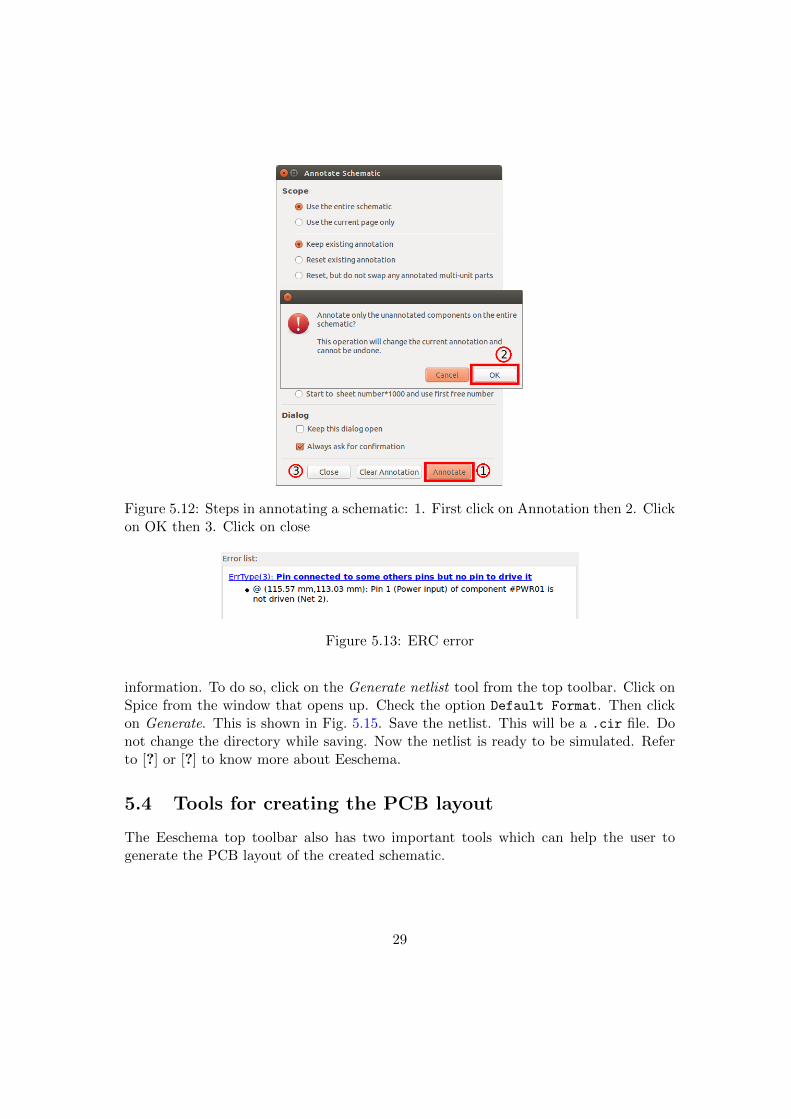
Figure 5.12: Steps in annotating a schematic: 1. First click on Annotation then 2. Clickon OK then 3. Click on close
Figure 5.13: ERC error
information. To do so, click on the Generate netlist tool from the top toolbar. Click onSpice from the window that opens up. Check the option Default Format. Then clickon Generate. This is shown in Fig. 5.15. Save the netlist. This will be a .cir file. Donot change the directory while saving. Now the netlist is ready to be simulated. Referto [?] or [?] to know more about Eeschema.
5.4 Tools for creating the PCB layout
The Eeschema top toolbar also has two important tools which can help the user togenerate the PCB layout of the created schematic.
29

Figure 5.14: Green arrow pointing to Ground terminal indicating an ERC error
Figure 5.15: Steps in generating a Netlist for simulation: 1. Click on Spice then2. Check the option Default Format then 3. Click on Generate
5.4.1 FootPrint Editor
Clicking on the Footprint Editor tool will open the CvPcb window. This window willideally open the .net file for the current project. So, before using this tool, one shouldhave the netlist for PCB design (a .net file). To know more about how to assignfootprints to components, see Chapter 12.
5.4.2 PCB Layout
Clicking on the Layout Editor tool will open Pcbnew, the layout editor used in eSim.In this window, one will create the PCB. It involves laying tracks and vias, performingoptimum routing of tracks, creating one or more copper layers for PCB, etc. It will besaved as a .brd file in the current project directory. Chapter 12 explains how to usethe Layout Editor to design a PCB.
30

Chapter 6
Simulation
Circuit simulation uses mathematical models to replicate the behaviour of an actualdevice or circuit. Simulation software allows to model circuit operations. Simulatinga circuit’s behaviour before actually building it can greatly improve design efficiency.eSim uses Ngspice for analog, digital and mixed-level/mixed-signal circuit simulation.The various steps involved in simulating a circuit schematic in eSim are explained inthe sections below:
6.1 Kicad to Ngspice Conversion
In the chapter on schematic creation, we have learnt to generate the netlist from circuitschematic. The generated netlist is not compatible with Ngspice. eSim uses Ngspiceto simulate the circuit schematic. Hence the netlist i.e. .cir file generated should beconverted in to a Ngspice compatible file. The Convert KiCad to Ngspice tool on eSimleft toolbar is used to do this. Let us now see the various tabs and their functionsavailable under this.
6.1.1 Analysis
In order to simulate a circuit, the user must define the type of analysis to be done onthe circuit. This tab is used to insert the type of analysis and value of the analysisparameters to the netlist. eSim supports three types of analyses: 1. DC Analysis (Op-erating Point and DC Sweep) 2. AC Small-signal Analysis 3. Transient Analysis Theseare explained below.
In the current example for simulating an RC circuit, select the analysis type astransient analysis and enter the values as shown in the Fig. 6.1.
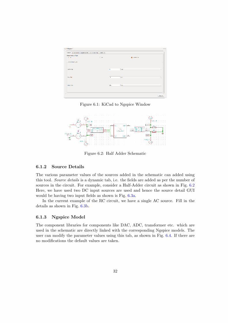
Figure 6.1: KiCad to Ngspice Window
Figure 6.2: Half Adder Schematic
6.1.2 Source Details
The various parameter values of the sources added in the schematic can added usingthis tool. Source details is a dynamic tab, i.e. the fields are added as per the number ofsources in the circuit. For example, consider a Half-Adder circuit as shown in Fig. 6.2Here, we have used two DC input sources are used and hence the source detail GUIwould be having two input fields as shown is Fig. 6.3a.
In the current example of the RC circuit, we have a single AC source. Fill in thedetails as shown in Fig. 6.3b.
6.1.3 Ngspice Model
The component libraries for components like DAC, ADC, transformer etc. which areused in the schematic are directly linked with the corresponding Ngspice models. Theuser can modify the parameter values using this tab, as shown in Fig. 6.4. If there areno modifications the default values are taken.
32

(a) Source Details of Half-Adder (b) Source Details of RC circuit
Figure 6.3: Source details interface
Figure 6.4: Half adder: Ngspice model
6.1.4 Device Modelling
Spice based simulators include a feature which allows accurate modeling of semiconduc-tor devices such as diodes, transistors etc. Model libraries holds these features to definemodels for devices such as diodes, MOSFET, BJT, JFET, IGBT, Magnetic core etc.
The fields in this tab are added for each such device in the circuit and the corre-sponding model library is added. In the example of bridge rectifier as shown in Fig. 6.5afor four diodes library files are added as in Fig. 6.5b. Location for these libraries is asfollowing :../Library/deviceModelLibrary/Diode/ if you are using version 2.0 and above
33
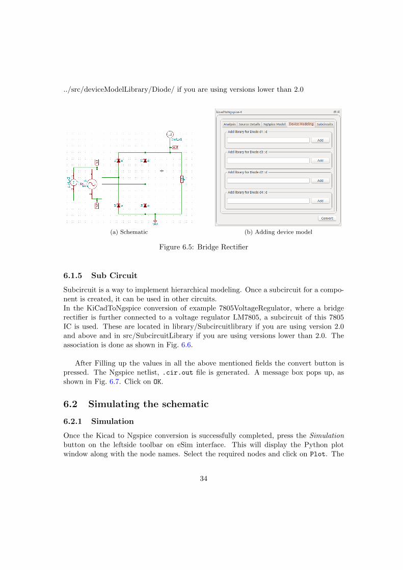
../src/deviceModelLibrary/Diode/ if you are using versions lower than 2.0
(a) Schematic (b) Adding device model
Figure 6.5: Bridge Rectifier
6.1.5 Sub Circuit
Subcircuit is a way to implement hierarchical modeling. Once a subcircuit for a compo-nent is created, it can be used in other circuits.In the KiCadToNgspice conversion of example 7805VoltageRegulator, where a bridgerectifier is further connected to a voltage regulator LM7805, a subcircuit of this 7805IC is used. These are located in library/Subcircuitlibrary if you are using version 2.0and above and in src/SubcircuitLibrary if you are using versions lower than 2.0. Theassociation is done as shown in Fig. 6.6.
After Filling up the values in all the above mentioned fields the convert button ispressed. The Ngspice netlist, .cir.out file is generated. A message box pops up, asshown in Fig. 6.7. Click on OK.
6.2 Simulating the schematic
6.2.1 Simulation
Once the Kicad to Ngspice conversion is successfully completed, press the Simulationbutton on the leftside toolbar on eSim interface. This will display the Python plotwindow along with the node names. Select the required nodes and click on Plot. The
34
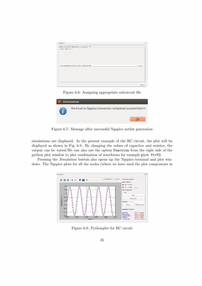
Figure 6.6: Assigning appropriate subcircuit file
Figure 6.7: Message after successful Ngspice netlist generation
simulations are displayed. In the present example of the RC circuit, the plot will bedisplayed as shown in Fig. 6.8. By changing the values of capacitor and resistor, theoutput can be varied.We can also use the option Function from the right side of thepython plot window to plot combination of waveforms for example plot V1+V2.
Pressing the Simulation button also opens up the Ngspice terminal and plot win-dows. The Ngspice plots for all the nodes (where we have used the plot components in
Figure 6.8: Pythonplot for RC circuit
35
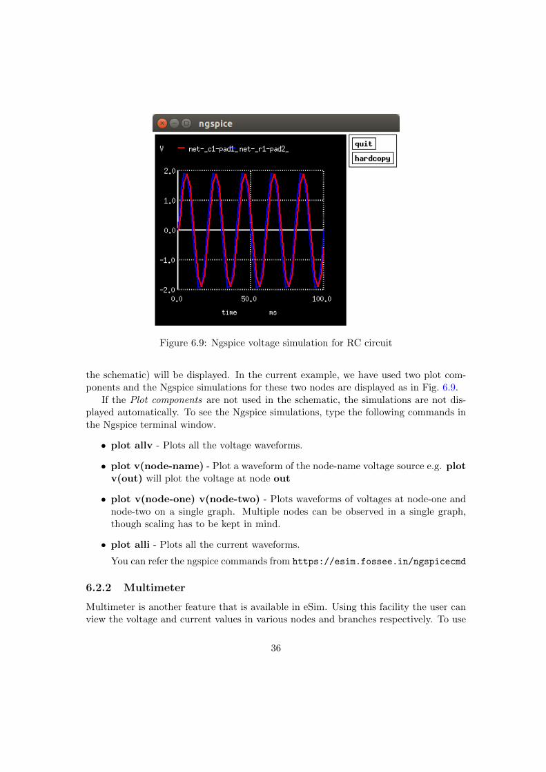
Figure 6.9: Ngspice voltage simulation for RC circuit
the schematic) will be displayed. In the current example, we have used two plot com-ponents and the Ngspice simulations for these two nodes are displayed as in Fig. 6.9.
If the Plot components are not used in the schematic, the simulations are not dis-played automatically. To see the Ngspice simulations, type the following commands inthe Ngspice terminal window.
• plot allv - Plots all the voltage waveforms.
• plot v(node-name) - Plot a waveform of the node-name voltage source e.g. plotv(out) will plot the voltage at node out
• plot v(node-one) v(node-two) - Plots waveforms of voltages at node-one andnode-two on a single graph. Multiple nodes can be observed in a single graph,though scaling has to be kept in mind.
• plot alli - Plots all the current waveforms.
You can refer the ngspice commands from https://esim.fossee.in/ngspicecmd
6.2.2 Multimeter
Multimeter is another feature that is available in eSim. Using this facility the user canview the voltage and current values in various nodes and branches respectively. To use
36
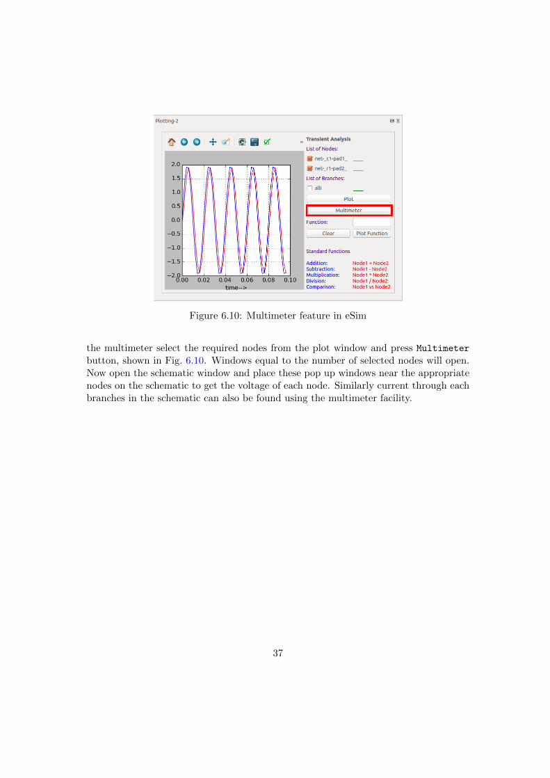
Figure 6.10: Multimeter feature in eSim
the multimeter select the required nodes from the plot window and press Multimeter
button, shown in Fig. 6.10. Windows equal to the number of selected nodes will open.Now open the schematic window and place these pop up windows near the appropriatenodes on the schematic to get the voltage of each node. Similarly current through eachbranches in the schematic can also be found using the multimeter facility.
37

Chapter 7
Model Editor
Spice based simulators include a feature which allows accurate modeling of semicon-ductor devices such as diodes, transistors etc. eSim Model Editor provides a facility todefine a new model for devices such as diodes, MOSFET, BJT, JFET, IGBT, Magneticcore etc. Model Editor in eSim lets the user enter the values of parameters depending onthe type of device for which a model is required. The parameter values can be obtainedfrom the data-sheet of the device. A newly created model can be exported to the modellibrary and one can import it for different projects, whenever required. Model Editoralso provides a facility to edit existing models. The GUI of the model editor is as shownin Fig. 7.1
7.1 Creating New Model Library
eSim lets us create new model libraries based on the template model libraries. Onselecting New button the window is popped as shown in Fig. 7.2. The name has to be
Figure 7.1: Model Editor

Figure 7.2: Creating New Model Library
Figure 7.3: Choosing the Template Model Library
unique otherwise the error message appears on the window.After the OK button is pressed the type of model library to be created is chosen by
selecting one of the types on the left hand side i.e. Diode, BJT, MOS, JFET, IGBT,
Magnetic Core. The template model library opens up in a tabular form as shown inFig. 7.3
39
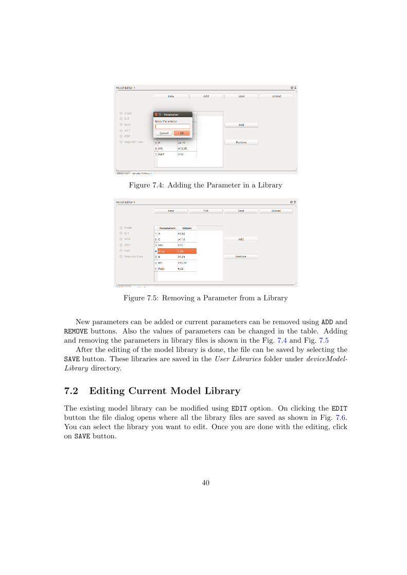
Figure 7.4: Adding the Parameter in a Library
Figure 7.5: Removing a Parameter from a Library
New parameters can be added or current parameters can be removed using ADD andREMOVE buttons. Also the values of parameters can be changed in the table. Addingand removing the parameters in library files is shown in the Fig. 7.4 and Fig. 7.5
After the editing of the model library is done, the file can be saved by selecting theSAVE button. These libraries are saved in the User Libraries folder under deviceModel-Library directory.
7.2 Editing Current Model Library
The existing model library can be modified using EDIT option. On clicking the EDIT
button the file dialog opens where all the library files are saved as shown in Fig. 7.6.You can select the library you want to edit. Once you are done with the editing, clickon SAVE button.
40
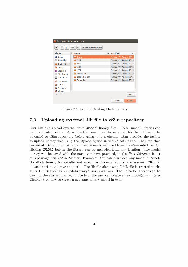
Figure 7.6: Editing Existing Model Library
7.3 Uploading external .lib file to eSim repository
User can also upload external spice .model library files. These .model libraries canbe downloaded online. eSim directly cannot use the external .lib file. It has to beuploaded to eSim repository before using it in a circuit. eSim provides the facilityto upload library files using the Upload option in the Model Editor . They are thenconverted into xml format, which can be easily modified from the eSim interface. Onclicking UPLOAD button the library can be uploaded from any location. The modellibrary will be saved with the name you have provided, in the User Libraries folderof repository deviceModelLibrary. Example: You can download any model of Schot-tky diode from Spice website and save it as .lib extension on the system. Click onUPLOAD option and give the path. The lib file along with XML file is created in theeSim-1.1.3/src/deviceModeLibrary/UserLibraries. The uploaded library can beused for the existing part eSim Diode or the user can create a new model(part). ReferChapter 8 on how to create a new part library model in eSim.
41
Chapter 8
SubCircuit Builder
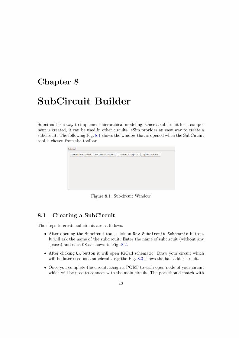
Subcircuit is a way to implement hierarchical modeling. Once a subcircuit for a compo-nent is created, it can be used in other circuits. eSim provides an easy way to create asubcircuit. The following Fig. 8.1 shows the window that is opened when the SubCircuittool is chosen from the toolbar.
Figure 8.1: Subcircuit Window
8.1 Creating a SubCircuit
The steps to create subcircuit are as follows.
• After opening the Subcircuit tool, click on New Subcircuit Schematic button.It will ask the name of the subcircuit. Enter the name of subcircuit (without anyspaces) and click OK as shown in Fig. 8.2.
• After clicking OK button it will open KiCad schematic. Draw your circuit whichwill be later used as a subcircuit. e.g the Fig. 8.3 shows the half adder circuit.
• Once you complete the circuit, assign a PORT to each open node of your circuitwhich will be used to connect with the main circuit. The port should match with
42

Figure 8.2: New Sub circuit Window
Figure 8.3: Inner circuit of the subcircuit
the number of input and output pin. The circuit will look like Fig. 8.4 after addingPORT to it. The PORT component can be found in the eSim Miscellaneouslibrary as shown in Fig. 8.5. Select a different port for each node (input or output),the PORT has 26 such components named alphabetically as Unit A, Unit B to UnitZ, meaning you can create a subcircuit up-to 26 pins(input, output combined).
• Next step is to save the schematic and generate KiCad netlist as explained inChapter 5.
• To use this subcircuit in other schematics, create a block in the schematic editorby following steps given below as one should have a symbol corresponding to thenewly created subcircuit that can be used in other schematics:
43

Figure 8.4: Half-Adder Subcircuit
Figure 8.5: Selection of PORT component
1. Go to library browser of the schematic editor. It is an ”open book with apencil in its middle” icon on the top toolbar.
2. Select the Current Library as eSim Subckt shown in Fig. 8.6
44
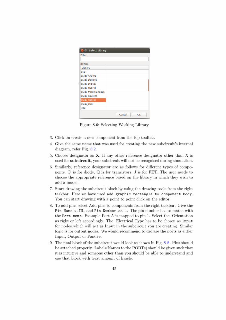
Figure 8.6: Selecting Working Library
3. Click on create a new component from the top toolbar.
4. Give the same name that was used for creating the new subcircuit’s internaldiagram, refer Fig. 8.2.
5. Choose designator as X. If any other reference designator other than X isused for subcircuit, your subcircuit will not be recognised during simulation.
6. Similarly, reference designator are as follows for different types of compo-nents. D is for diode, Q is for transistors, J is for FET. The user needs tochoose the appropriate reference based on the library in which they wish toadd a model.
7. Start drawing the subcircuit block by using the drawing tools from the righttaskbar. Here we have used Add graphic rectangle to component body.You can start drawing with a point to point click on the editor.
8. To add pins select Add pins to components from the right taskbar. Give thePin Name as IN1 and Pin Number as 1. The pin number has to match withthe Port name. Example Port A is mapped to pin 1. Select the Orientationas right or left accordingly. The Electrical Type has to be chosen as Input
for nodes which will act as Input in the subcircuit you are creating. Similarlogic is for output nodes. We would recommend to declare the ports as eitherInput, Output or Passive.
9. The final block of the subcircuit would look as shown in Fig. 8.8. Pins shouldbe attached properly. Labels(Names to the PORTs) should be given such thatit is intuitive and someone other than you should be able to understand anduse that block with least amount of hassle.
45

Figure 8.7: Creating New Component
10. In order to save this file, press Ctrl+S keys and click yes for confirmationpurposes.
11. Note : A good practice to retain this created subcircuit would be to takea backup of this library. To do that, click on File from the library editorwindow and select the Save Current Library as option. A location needsto be selected, please select eSim-Workspace as the location for storing thisfile and give relevant name e.g. eSim-Subckt-backup. Later other userscan use this in their circuits.
Specifying parameters for generating the .sub file
1. A .sub file is nothing but textual representation that is passed to the simu-lator which essentially informs the simulator about the nodes, and behaviorof the subcircuit block. Remember the Fig. 8.4 circuit? It will be saved in a.sub file once we complete this process!
2. Switch to the eSim main window and click on Convert KiCad to Ngspicebutton in the subcircuit builder tool. as shown in Fig. 8.1
3. You need not assign any values in the transient parameters section.Assign the values to any voltage or current sources present in your internalcircuit, if any.Add the appropriate device libraries or subcircuit libraries if you have usedany Device Models or Subcircuits, if any.
46

Figure 8.8: Half-Adder Subcircuit Block
4. Upon successful generation of the subcircuit file, an acknowledgement mes-
sage will be displayed. To confirm, go to
For Windows OS users :C:/FOSSEE/eSim/Library/SubcircuitLibrary if you are using v2.0 andaboveC:/FOSSEE/eSim/src/SubcircuitLibrary if you are using versions lowerthan 2.0
For Ubuntu Linux Users../eSim-2.0/Library/SubcircuitLibrary if you are using v2.0 and above../eSim-1.1.3/src/SubcircuitLibrary if you are using versions lower than2.0And make sure that the .sub file is present under the directory carryingthe name of the subcircuit that you specified in step in Fig. 8.2.
8.2 Edit a Subcircuit
The steps to edit a subcircuit are as follows.
• After launching the Subcircuit tool, click on Edit Subcircuit Schematic button.It will open a dialog box where you can select any subcircuit for editing.
47
• After selecting the subcircuit it will open it in the schematic editor, where youcan edit the subcircuit.
• Next step is to save the schematic and generate the .cir netlist.
• If you have edited the number of ports then you have to change the block exaplainedin section Creating a Subcircuit accordingly.
Note:
• User can also import or append the schematic of different projects in the cur-rent page using the Append Schematic Sheet from the File menu. This will im-port(copy) the schematic that user has defined to the current schematic editorpage.
• User can also import the model in the part library editor page using the optionImport Component from the top toolbar.
8.3 Upload subcircuit
• Using this feature, one can import an existing subcircuit file into eSim environ-ment. You necessarily need not create the schematic for this.
• Download the required subcircuit’s .sub file from many online resources/repositories.
• Upload this file using the upload subcircuit feature.
• Upon uploading following checks will be made, and only and only if the checksare satisfied, the file will be uploaded. The checks are as following :1. The uploaded file should have the extension .sub2. The name of the file, say for example is omega.sub, then the content of thefile must start with .subckt omega and end with .ends omega.Any line that starts with asterisk sign(*) is considered as a comment in thesetypes of files. Hence, the file technically starts with .subckt.
• If above conditions are satisfied, then the file will be automatically placed ina folder that carries the same name as that of the .sub file will be created in../SubcircuitLibrary/ directory.
• Once above steps are verified, proceed to create a block as shown in Fig. 8.8 andname should be same as that of the corresponding .sub file uploaded earlier. Pinsof this block should match the number of pins stated in the .sub file.NOTE: ONLY AND ONLY THE OUTER BLOCK NEEDS TO BE CREATED.INTERNAL CIRCUIT IS NOT REQUIRED IF YOU ARE USING THE UP-LOAD FEATURE.
48

Chapter 9
NGHDL-Mixed Signal Simulation
NGHDL feature facilitates creation of user-defined models for mixed-signal circuit simu-lation in eSim. By interfacing GHDL and Ngspice, we achieve mixed-signal simulation.Digital models are simulated using GHDL and XSpice engine of Ngspice.
9.1 Introduction
Ngspice supports mixed-signal simulation, i.e. it can simulate both digital and analogcomponent. It defines a model which has the functionality of the circuit component,which can be used in the netlist. For example you can create an adder model in Ngspiceand use it in any circuit netlist of Ngspice.
However, it is not feasible to define complex digital models without a complete un-derstanding of Ngspice and XSPICE architectures and is a time-consuming process.Also, most of the users are familiar with GHDL and can write the models using VHDLcode with ease. Hence, NGHDL provides an interface to write VHDL code for a digitalmodel and install it as model in Ngspice. So whenever Ngspice looks for that model, itwill actually interface with VHDL code to get the result.
Fig. 9.1 shows the overview of NGHDL indicating its architecture at the abstractlevel. The values for the digital models present in the netlist are fetched from theGHDL side of the interface whereas the values of the analog part are fetched fromNgspice’s spice3f5 engine. Digital and Analog components in Fig. 9.1 are connected toeach other with the help of the hybrid ADC and DAC models provided by Ngspice.This helps in the signal level switching when simulation is performed. As analog signalsare in continuous time domain and Digital signals are in discrete time domain, hybridcomponents help bridge the gap. More information on the parameters of ADC and DAC
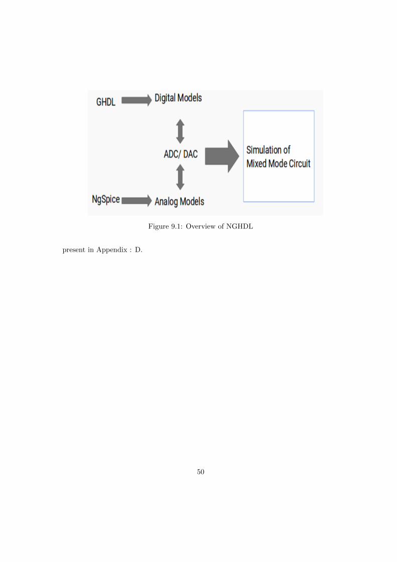
Figure 9.1: Overview of NGHDL
present in Appendix : D.
50
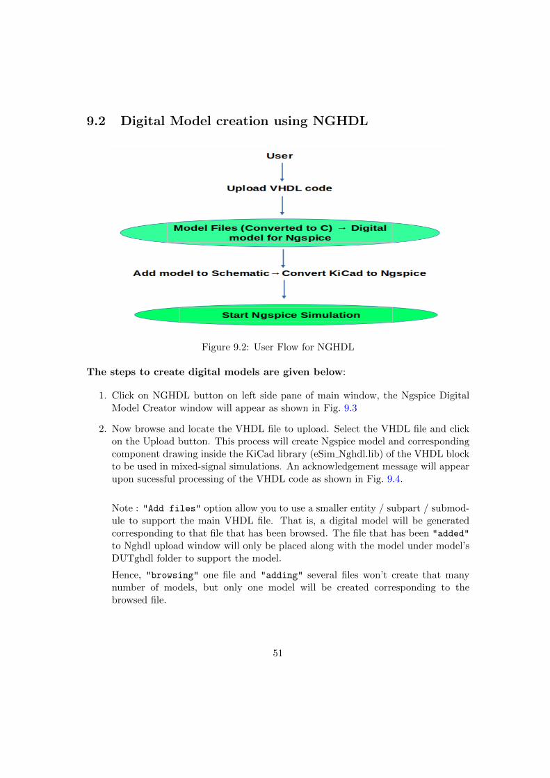
9.2 Digital Model creation using NGHDL
Figure 9.2: User Flow for NGHDL
The steps to create digital models are given below:
1. Click on NGHDL button on left side pane of main window, the Ngspice DigitalModel Creator window will appear as shown in Fig. 9.3
2. Now browse and locate the VHDL file to upload. Select the VHDL file and clickon the Upload button. This process will create Ngspice model and correspondingcomponent drawing inside the KiCad library (eSim Nghdl.lib) of the VHDL blockto be used in mixed-signal simulations. An acknowledgement message will appearupon sucessful processing of the VHDL code as shown in Fig. 9.4.
Note : "Add files" option allow you to use a smaller entity / subpart / submod-ule to support the main VHDL file. That is, a digital model will be generatedcorresponding to that file that has been browsed. The file that has been "added"
to Nghdl upload window will only be placed along with the model under model’sDUTghdl folder to support the model.
Hence, "browsing" one file and "adding" several files won’t create that manynumber of models, but only one model will be created corresponding to thebrowsed file.
51
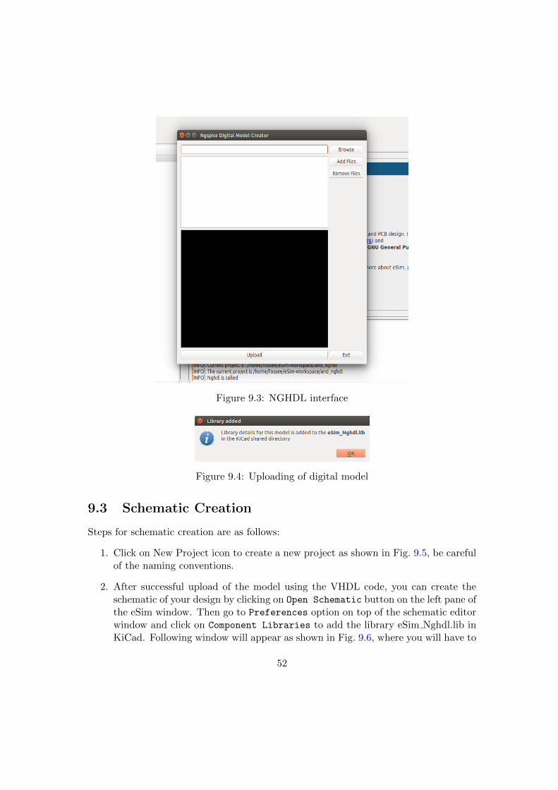
Figure 9.3: NGHDL interface
Figure 9.4: Uploading of digital model
9.3 Schematic Creation
Steps for schematic creation are as follows:
1. Click on New Project icon to create a new project as shown in Fig. 9.5, be carefulof the naming conventions.
2. After successful upload of the model using the VHDL code, you can create theschematic of your design by clicking on Open Schematic button on the left pane ofthe eSim window. Then go to Preferences option on top of the schematic editorwindow and click on Component Libraries to add the library eSim Nghdl.lib inKiCad. Following window will appear as shown in Fig. 9.6, where you will have to
52

Figure 9.5: Creation of a new project
click on Add button and select the eSim Nghdl library. Refer Fig. 9.6 and Fig. 9.7.
Figure 9.6: Adding the digital model library in KiCad
53
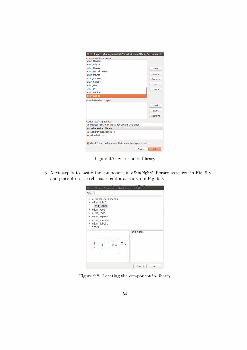
Figure 9.7: Selection of library
3. Next step is to locate the component in eSim Nghdl library as shown in Fig. 9.8and place it on the schematic editor as shown in Fig. 9.9.
Figure 9.8: Locating the component in library
54
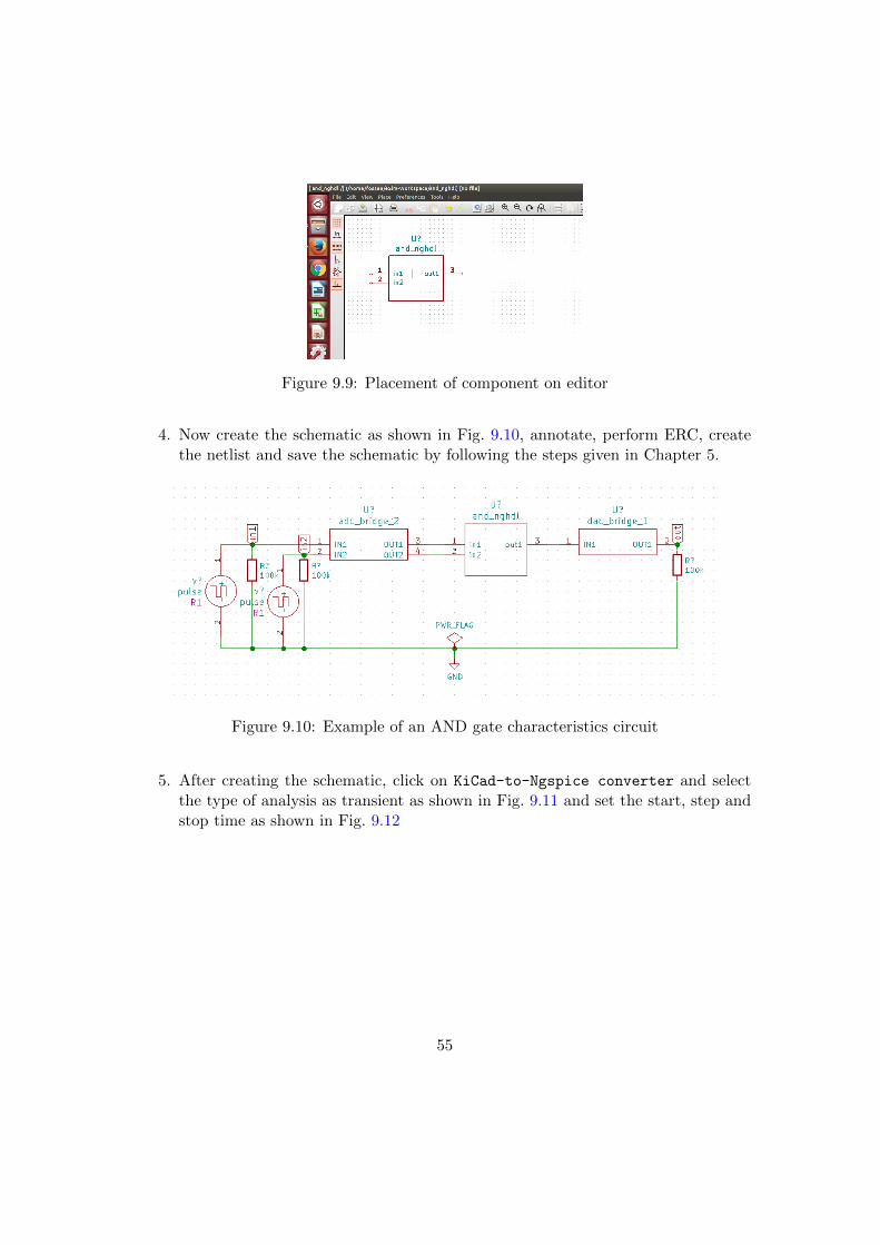
Figure 9.9: Placement of component on editor
4. Now create the schematic as shown in Fig. 9.10, annotate, perform ERC, createthe netlist and save the schematic by following the steps given in Chapter 5.
Figure 9.10: Example of an AND gate characteristics circuit
5. After creating the schematic, click on KiCad-to-Ngspice converter and selectthe type of analysis as transient as shown in Fig. 9.11 and set the start, step andstop time as shown in Fig. 9.12
55
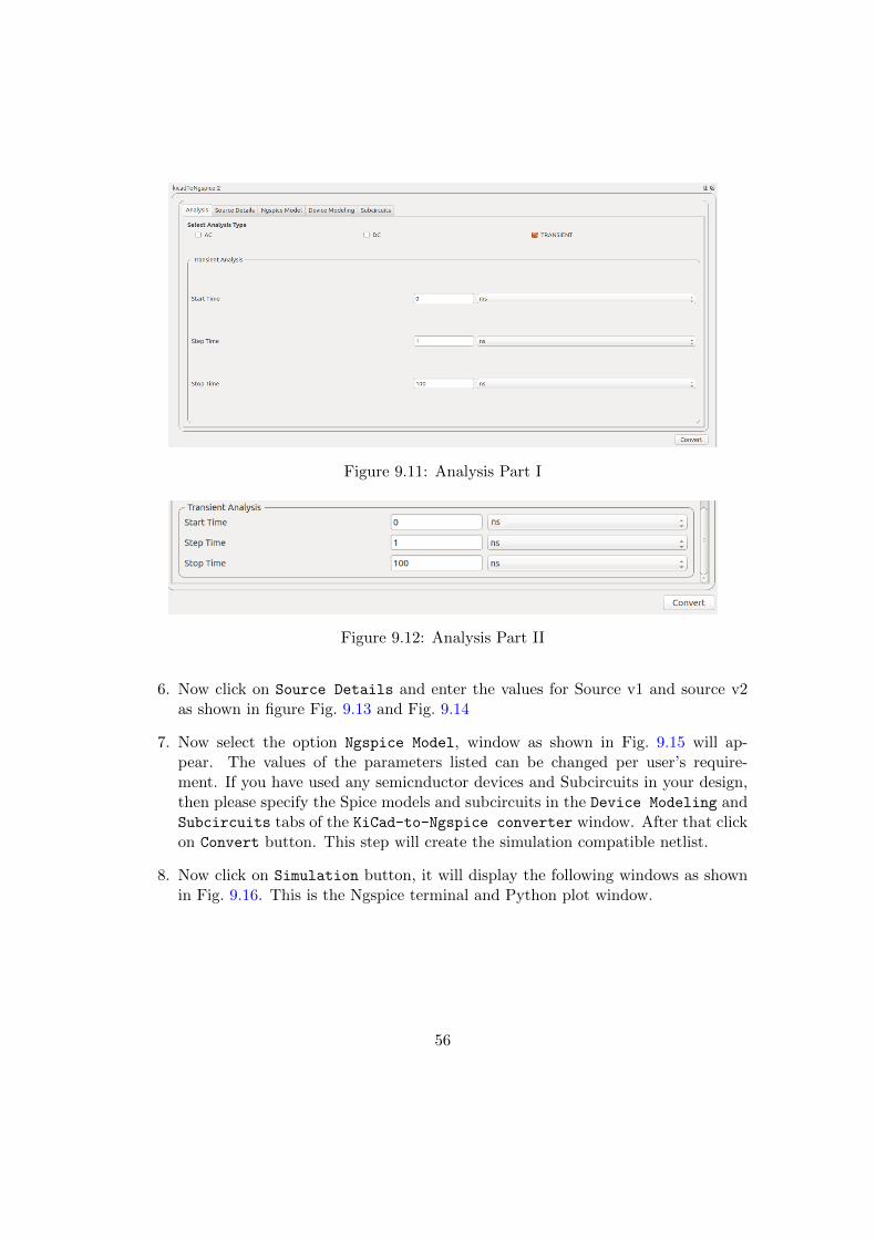
Figure 9.11: Analysis Part I
Figure 9.12: Analysis Part II
6. Now click on Source Details and enter the values for Source v1 and source v2as shown in figure Fig. 9.13 and Fig. 9.14
7. Now select the option Ngspice Model, window as shown in Fig. 9.15 will ap-pear. The values of the parameters listed can be changed per user’s require-ment. If you have used any semicnductor devices and Subcircuits in your design,then please specify the Spice models and subcircuits in the Device Modeling andSubcircuits tabs of the KiCad-to-Ngspice converter window. After that clickon Convert button. This step will create the simulation compatible netlist.
8. Now click on Simulation button, it will display the following windows as shownin Fig. 9.16. This is the Ngspice terminal and Python plot window.
56
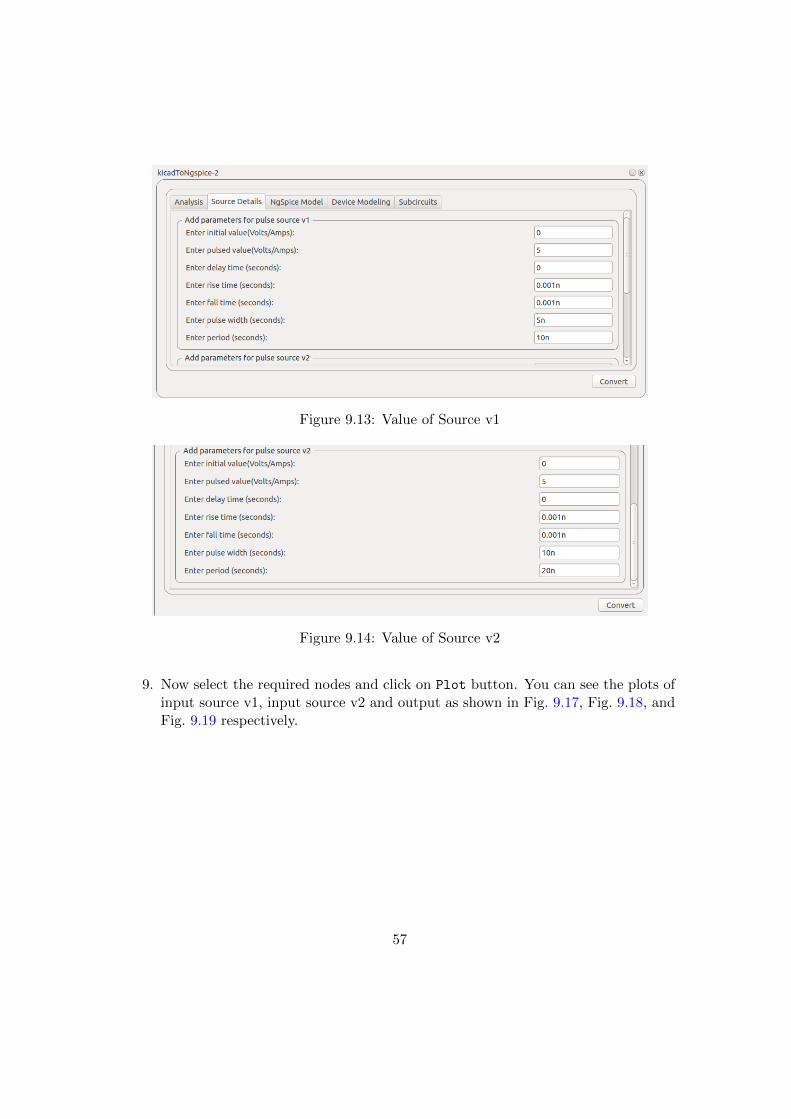
Figure 9.13: Value of Source v1
Figure 9.14: Value of Source v2
9. Now select the required nodes and click on Plot button. You can see the plots ofinput source v1, input source v2 and output as shown in Fig. 9.17, Fig. 9.18, andFig. 9.19 respectively.
57
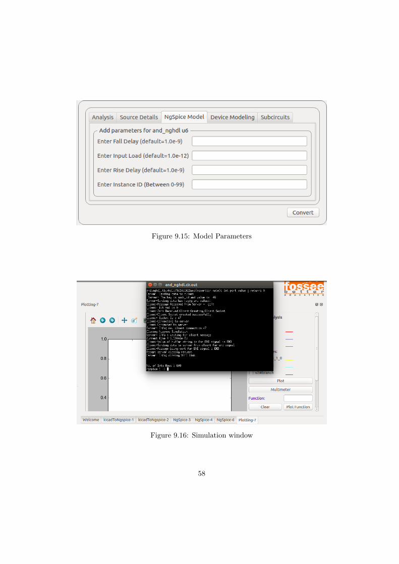
Figure 9.15: Model Parameters
Figure 9.16: Simulation window
58

Figure 9.17: Plot of Source V1
Figure 9.18: Plot of source V2
59

Figure 9.19: Plot of output
60

Chapter 10
OpenModelica
10.1 Introduction
OpenModelica (OM) is an open source modeling and simulation tool based on Modelicalanguage. Modelica is an object oriented language. As a result, it has all the featuresof an object oriented language such as inheritance. Models or circuits are defined inthe form of classes, with in which there are components, functions, connection andplacement information. The OM suite has the following major tools.
10.1.1 OMEdit
An IDE for modeling and simulation. It supports a lot of electrical components. It hasa good graphical interface to drag and drop components and create the circuit. Onecan only do transient simulation using this interface. An attractive feature of OMEditis the plotting interface. All the parameters in the circuit like voltages and currentsthrough each component, parameters like frequency, delay etc. will be displayed as alist, after simulation. The user can choose the variables to be plotted in an interactivemanner from this list. On choosing the variable to plot, it will be plotted on the plotwindow. One can also create multiple plot windows.
10.1.2 OMOptim
An IDE for optimisation. It lists all the variables in the given model. One can choosethe variables to be optimised from the list. Multiple models can be loaded for a givenoptimisation problem. One can do multi objective optimisations as well. It supportsvarious optimisation algorithms such as Particle Swarm Optimisation (PSO) and Sim-ulated Annealing (SA). The results are displayed graphically.

10.2 OpenModelica in eSim
The above two functionalities can be accessed through the Modelica Converter and OM
Optimisation tools on the eSim left toolbar. The two examples given below illustrateshow to use OpenModelica in eSim.
Low Pass Filter circuit
Let us now see how to simulate a low pass filter in OpenModelica.
1. Open the schematic and create the circuit as shown in Fig. 10.1.
Figure 10.1: Circuit schematic: Low pass filter
2. Create the KiCad netlist. Now the analysis and analysis parameters are given asshown in Fig. 10.2.
3. The source details are given as in Fig. 10.3. The generated KiCad netlist is thenconverted to ngspice compatible netlist.
4. Simulate the ngspice netlist. The simulation curves are shown in Fig. 10.4.
5. Now to use OpenModelica, click on Modelica Converter in the bottom left ofeSim left toolbar.M ake sure you have OpenModelica installed in the system. Thisconverter converts the spice netlist to Modelica format. Click on the LPF in the
62

Figure 10.2: Analysis parameters: Low pass filter
Figure 10.3: Source details: Low pass filter
left that is appended in OpenModelica main window. Make sure you are in textview to see the Modelica code as shown in Fig. 10.5 Figure shows that LPF circuitis being used as a model, the initialisation of sources and components are in thebeginning followed by the connection information. n3, n0,n2 are the nodes.
Default Modelica libary is used for electrical sources and components. This hasto imported so that it can be used in the current circuit. This is available in theleft side of main window.
6. Click on Simulation Setup on the toolbar at the top. A window opens as shownin Fig. 10.6. Give start and stop time. Click OK.
7. A plotting window opens. Click on the node at the right to display the waveform.The window is shown in Fig. 10.7.
10.2.1 OM Optimisation
Now let us explore how to use OpenModelica for optimisation through an example.Find the value of resistance R2 that maximises the power dissipated through it for the
63

Figure 10.4: Simulation: Low pass filter
Figure 10.5: OpenModelica: Text view
circuit in Fig. 10.8. This is an illustration of the Maximum Power Transfer Theorem.The power is maximum when R2 = R1, i.e., when R2 = 100. So maximum power wouldbe Pmax = 0.0625. Let us now see the steps to be followed find the value of R2 usingeSim.
1. Follow all the steps as above and generate the Modelica model using the Ngspiceto Modelica converter.
2. The objective function is Power = i2×R2 . To define the objective function, theline power := i2 × R1 + i2 × R2 is added under the keyword algorithm, in the
64

Figure 10.6: OpenModelica: Simulation setup
Figure 10.7: OpenModelica: Simulation
Modelica model file.
3. Select OMOptim from eSim left toolbar, in the displayed window click on New
65
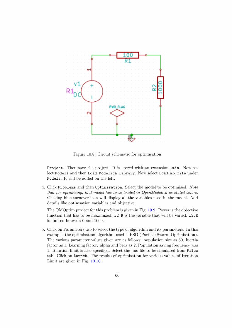
Figure 10.8: Circuit schematic for optimisation
Project. Then save the project. It is stored with an extension .min. Now se-lect Models and then Load Modelica Library. Now select Load mo file underModels. It will be added on the left.
4. Click Problems and then Optimisation. Select the model to be optimised. Notethat for optimising, that model has to be loaded in OpenModelica as stated before.Clicking blue turnover icon will display all the variables used in the model. Adddetails like optimsation variables and objective.
The OMOptim project for this problem is given in Fig. 10.9. Power is the objectivefunction that has to be maximized. r2.R is the variable that will be varied. r2.Ris limited between 0 and 1000.
5. Click on Parameters tab to select the type of algorithm and its parameters. In thisexample, the optimisation algorithm used is PSO (Particle Swarm Optimisation).The various parameter values given are as follows: population size as 50, Inertiafactor as 1, Learning factor: alpha and beta as 2, Population saving frequency was1. Iteration limit is also specified. Select the .mo file to be simulated from Files
tab. Click on Launch. The results of optimisation for various values of IterationLimit are given in Fig. 10.10.
66
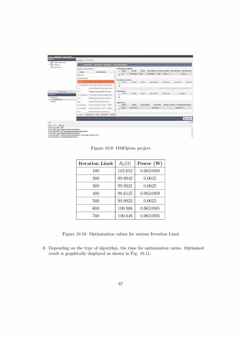
Figure 10.9: OMOptim project
Figure 10.10: Optimisation values for various Iteration Limit
6. Depending on the type of algorithm, the time for optimisation varies. Optimisedresult is graphically displayed as shown in Fig. 10.11.
67
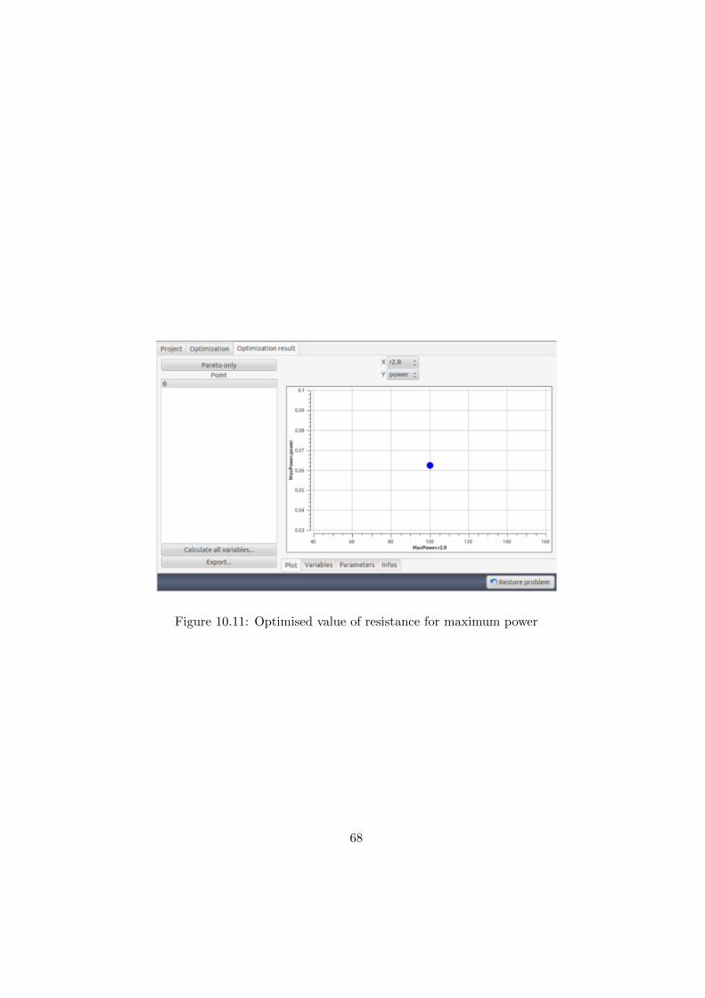
Figure 10.11: Optimised value of resistance for maximum power
68

Chapter 11
Solved Examples
11.1 Solved Examples
11.1.1 Basic RC Circuit
Problem Statement:
Plot the Input and Output Waveform of an RC circuit whose input voltage (Vs) is50Hz, 3V peak to peak. The values of Resistor (R) and Capacitor(C) are 1k and 1ufrespectively.
Solution:
• Creating a Project: The new project is created by clicking the New icon on themenubar. The name of the project is given in the pop up window as shown inFig. 11.1.
• Creating the Schematic: To create the schematic, click the very first icon of theleft toolbar as shown in the Fig. 11.2. This will open KiCad Eeschema.
To create a schematic in KiCad, we need to place the required components.Fig. 11.3 shows the icon on the right toolbar which opens the component library.

Figure 11.1: Creating New Project
Figure 11.2: Open Schematic Editor
After all the required components of the simple RC circuit are placed, wiring isdone using the Place Wire option as shown in the Fig. 11.4
70
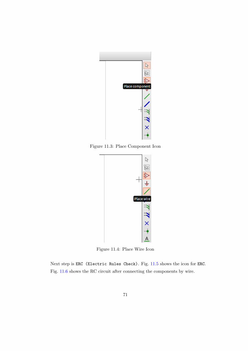
Figure 11.3: Place Component Icon
Figure 11.4: Place Wire Icon
Next step is ERC (Electric Rules Check). Fig. 11.5 shows the icon for ERC.
Fig. 11.6 shows the RC circuit after connecting the components by wire.
71
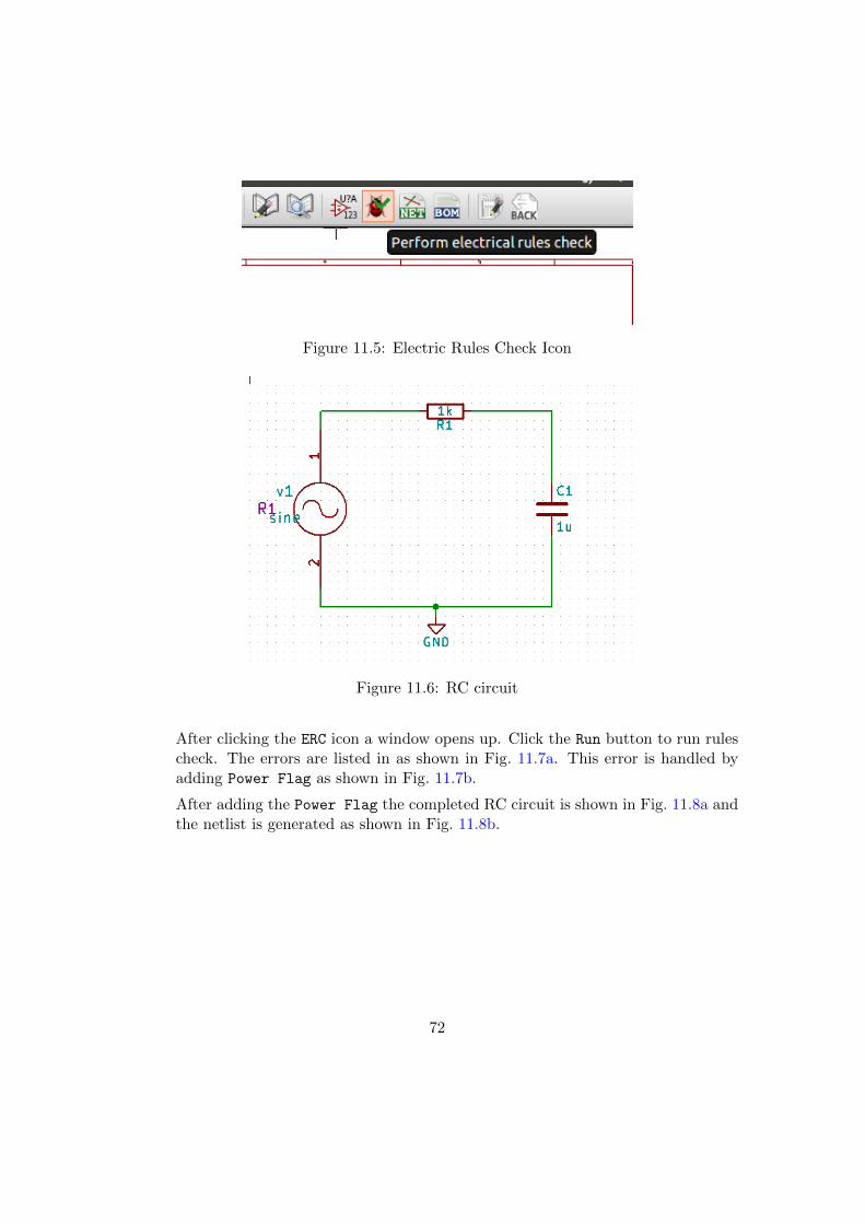
Figure 11.5: Electric Rules Check Icon
Figure 11.6: RC circuit
After clicking the ERC icon a window opens up. Click the Run button to run rulescheck. The errors are listed in as shown in Fig. 11.7a. This error is handled byadding Power Flag as shown in Fig. 11.7b.
After adding the Power Flag the completed RC circuit is shown in Fig. 11.8a andthe netlist is generated as shown in Fig. 11.8b.
72

(a) ERC Run (b) Power Flag
Figure 11.7: ERC check and POWER FLAG
(a) Schematic of RC circuit (b) Generating KiCad Netlist of RC circuit
Figure 11.8: RC Schematic and Netlist Generation
• Convert KiCad to Ngspice: To convert KiCad netlist of RC circuit to NgSpicecompatible netlist click on KiCad to Ngspice icon as shown in Fig. 11.9.
Now you can enter the type of analysis and source details as shown in Fig. 11.10aand Fig. 11.10b respectively.
The other tab will be empty as RC circuit do not use any Ngspice model, devicelibrary and subcircuit.
After entering the value, press the convert button. It will convert the netlist intoNgspice compatible netlist.
73
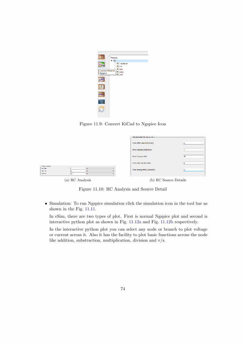
Figure 11.9: Convert KiCad to Ngspice Icon
(a) RC Analysis (b) RC Source Details
Figure 11.10: RC Analysis and Source Detail
• Simulation: To run Ngspice simulation click the simulation icon in the tool bar asshown in the Fig. 11.11.
In eSim, there are two types of plot. First is normal Ngspice plot and second isinteractive python plot as shown in Fig. 11.12a and Fig. 11.12b respectively.
In the interactive python plot you can select any node or branch to plot voltageor current across it. Also it has the facility to plot basic functions across the nodelike addition, substraction, multiplication, division and v/s.
74
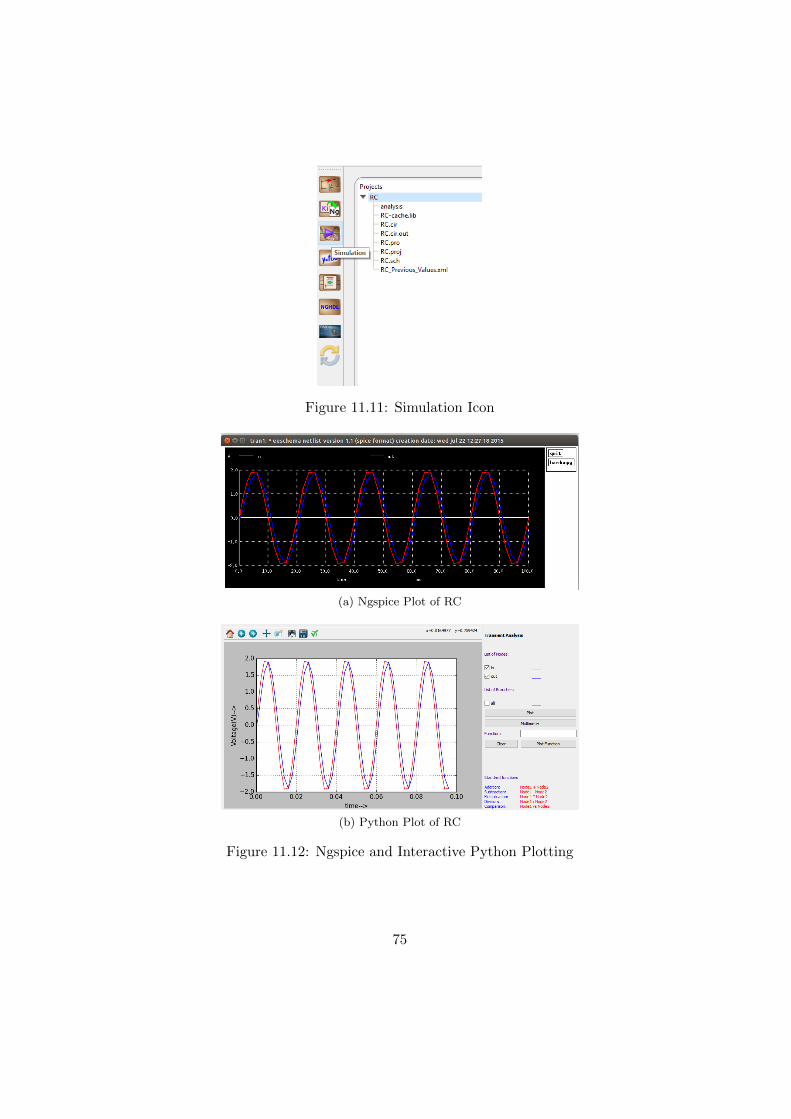
Figure 11.11: Simulation Icon
(a) Ngspice Plot of RC
(b) Python Plot of RC
Figure 11.12: Ngspice and Interactive Python Plotting
75

11.1.2 Half Wave Rectifier
Problem Statement:
Plot the Input and Output Waveform of Half Wave Rectifier circuit where the inputvoltage (Vs) is 50Hz, 2V peak to peak. The value for Resistor (R) is 1k.
Solution:
The new project is created by clicking the New icon on the menubar. The name of theproject is given in the window shown in Fig. 11.1.
• Creating Schematic: To create the schematic, click the very first icon of the lefttoolbar as shown in the Fig. 11.2. This will open KiCad Eeschema.
After the KiCad window is opened, to create a schematic we need to place therequired components. Fig. 11.3 shows the icon on the right toolbar which opensthe component library.
After all the required components of the simple Half Wave rectifier circuits areplaced, wiring is done using the Place Wire option as shown in the Fig. 11.4
Next step is ERC (Electric Rules Check). Fig. 11.5 shows the icon for ERC.After completing all the above steps the final Half Wave Rectifier schematic willlook like Fig. 11.13.
76

Figure 11.13: Schematic of Half Wave Rectifier circuit
KiCad netlist is generated as shown in the Fig. 11.14
Figure 11.14: Half Wave Rectifier circuit Netlist Generation
• Convert KiCad to Ngspice: After creating KiCad netlist, click on the KiCad-Ngspiceconverter button. This will open converter window where you can enter detailsof Analysis, Source values and Device library.
77

(a) Half Wave Rectifier Analysis (b) Half Wave Rectifier Source Details
(c) Half Wave Rectifier Device Modeling
Figure 11.15: Analysis, Source and Device Tab
Under device library you can add the library for diode used in the circuit. If youdo not add any library it will take default Ngspice model.
• Simulation: Once the KiCad-Ngspice converter runs successfully, you can runsimulation by clicking the simulation button in the toolbar.
78
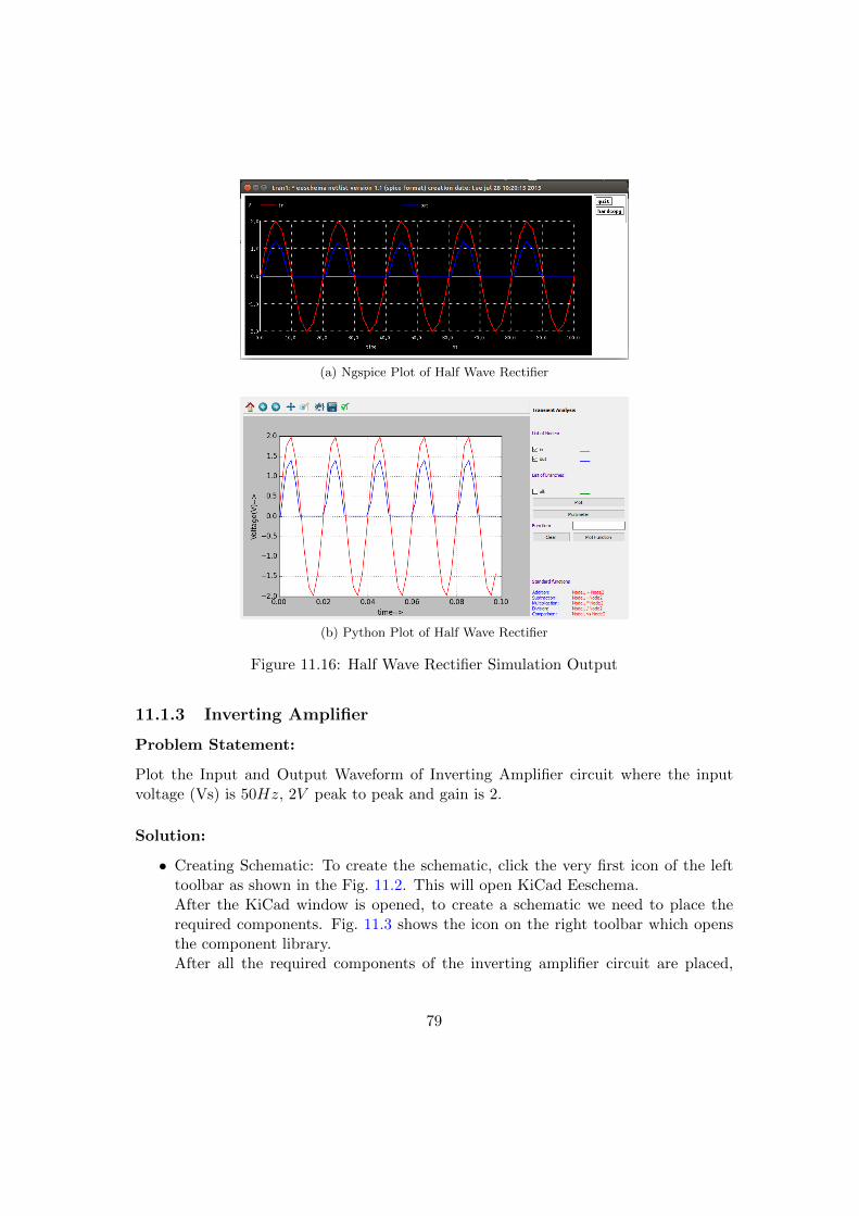
(a) Ngspice Plot of Half Wave Rectifier
(b) Python Plot of Half Wave Rectifier
Figure 11.16: Half Wave Rectifier Simulation Output
11.1.3 Inverting Amplifier
Problem Statement:
Plot the Input and Output Waveform of Inverting Amplifier circuit where the inputvoltage (Vs) is 50Hz, 2V peak to peak and gain is 2.
Solution:
• Creating Schematic: To create the schematic, click the very first icon of the lefttoolbar as shown in the Fig. 11.2. This will open KiCad Eeschema.After the KiCad window is opened, to create a schematic we need to place therequired components. Fig. 11.3 shows the icon on the right toolbar which opensthe component library.After all the required components of the inverting amplifier circuit are placed,
79
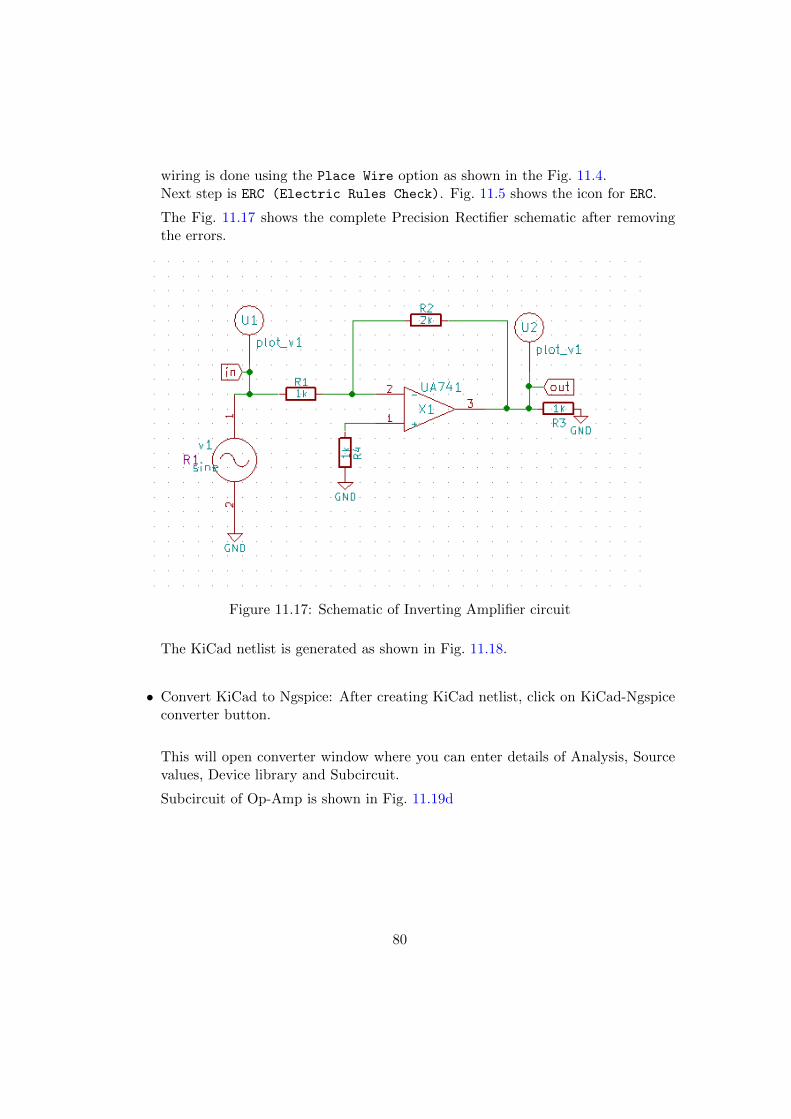
wiring is done using the Place Wire option as shown in the Fig. 11.4.Next step is ERC (Electric Rules Check). Fig. 11.5 shows the icon for ERC.
The Fig. 11.17 shows the complete Precision Rectifier schematic after removingthe errors.
Figure 11.17: Schematic of Inverting Amplifier circuit
The KiCad netlist is generated as shown in Fig. 11.18.
• Convert KiCad to Ngspice: After creating KiCad netlist, click on KiCad-Ngspiceconverter button.
This will open converter window where you can enter details of Analysis, Sourcevalues, Device library and Subcircuit.
Subcircuit of Op-Amp is shown in Fig. 11.19d
80

Figure 11.18: Inverting Amplifier circuit Netlist Generation
(a) Inverting Amplifier Analysis (b) Inverting Amplifier Source Details
(c) Inverting Amplifier Subcircuit
(d) Sub-Circuit of Op-Amp
Figure 11.19: Analysis, Source, and Subcircuit tab
Under subcircuit tab you have to add the subciruit used in your circuit. If youforget to add subcircuit, it will throw an error.
81
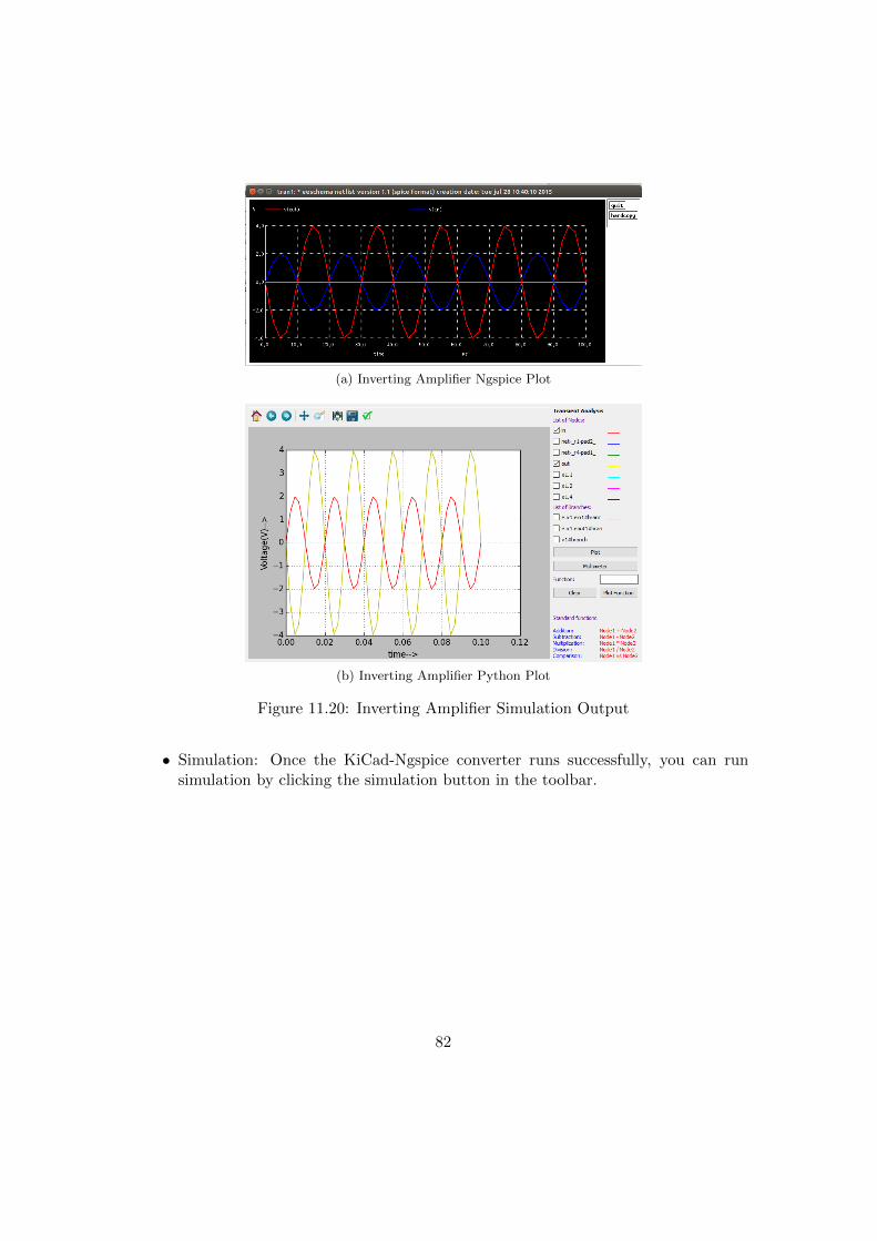
(a) Inverting Amplifier Ngspice Plot
(b) Inverting Amplifier Python Plot
Figure 11.20: Inverting Amplifier Simulation Output
• Simulation: Once the KiCad-Ngspice converter runs successfully, you can runsimulation by clicking the simulation button in the toolbar.
82
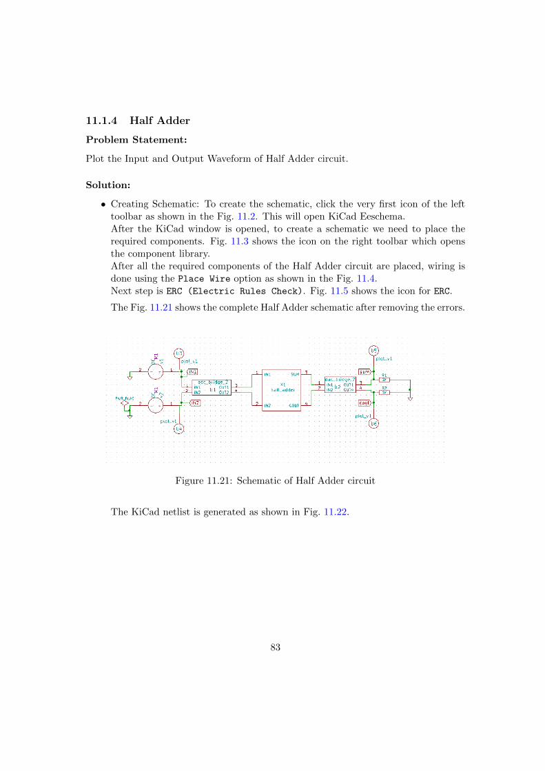
11.1.4 Half Adder
Problem Statement:
Plot the Input and Output Waveform of Half Adder circuit.
Solution:
• Creating Schematic: To create the schematic, click the very first icon of the lefttoolbar as shown in the Fig. 11.2. This will open KiCad Eeschema.After the KiCad window is opened, to create a schematic we need to place therequired components. Fig. 11.3 shows the icon on the right toolbar which opensthe component library.After all the required components of the Half Adder circuit are placed, wiring isdone using the Place Wire option as shown in the Fig. 11.4.Next step is ERC (Electric Rules Check). Fig. 11.5 shows the icon for ERC.
The Fig. 11.21 shows the complete Half Adder schematic after removing the errors.
Figure 11.21: Schematic of Half Adder circuit
The KiCad netlist is generated as shown in Fig. 11.22.
83
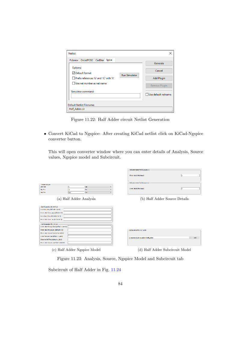
Figure 11.22: Half Adder circuit Netlist Generation
• Convert KiCad to Ngspice: After creating KiCad netlist click on KiCad-Ngspiceconverter button.
This will open converter window where you can enter details of Analysis, Sourcevalues, Ngspice model and Subcircuit.
(a) Half Adder Analysis (b) Half Adder Source Details
(c) Half Adder Ngspice Model (d) Half Adder Subcircuit Model
Figure 11.23: Analysis, Source, Ngspice Model and Subcircuit tab
Subcircuit of Half Adder in Fig. 11.24
84

Figure 11.24: Half Adder Subcircuit
• Simulation: Once the KiCad-Ngspice converter runs successfully, you can runsimulation by clicking the simulation button in the toolbar.
(a) Half Adder Ngspice Plot
(b) Half Adder Python Plot
Figure 11.25: Half Adder Simulation Output
85

11.1.5 Full Wave Rectifier using SCR
Problem Statement:
Plot the Input and Output Waveform of Full Wave Rectifier using SCR.
Solution:
• Creating Schematic: To create the schematic, click the very first icon of the lefttoolbar as shown in the Fig. 11.2. This will open KiCad Eeschema.After the KiCad window is opened, to create a schematic we need to place therequired components. Fig. 11.3 shows the icon on the right toolbar which opensthe component library.After all the required components of the Full Wave Rectifier using SCR circuit areplaced, wiring is done using the Place Wire option as shown in the Fig. 11.4.Next step is ERC (Electric Rules Check). Fig. 11.5 shows the icon for ERC.
The Fig. 11.26 shows the complete Rectifier circuit using SCR after removing theerrors.
Figure 11.26: Schematic of Full Wave Rectifier using SCR
86

The KiCad netlist is generated as shown in Fig. 11.27.
Figure 11.27: Full Wave Rectifier using SCR Netlist Generation
87
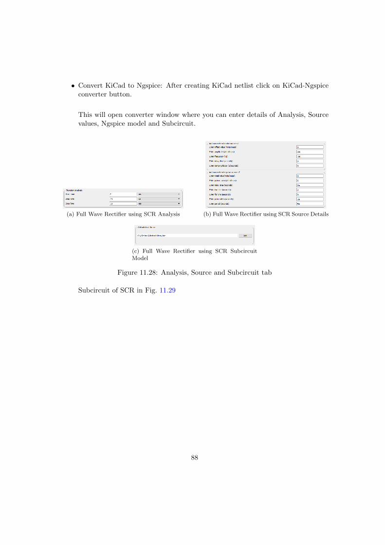
• Convert KiCad to Ngspice: After creating KiCad netlist click on KiCad-Ngspiceconverter button.
This will open converter window where you can enter details of Analysis, Sourcevalues, Ngspice model and Subcircuit.
(a) Full Wave Rectifier using SCR Analysis (b) Full Wave Rectifier using SCR Source Details
(c) Full Wave Rectifier using SCR SubcircuitModel
Figure 11.28: Analysis, Source and Subcircuit tab
Subcircuit of SCR in Fig. 11.29
88

Figure 11.29: SCR Subcircuit
• Simulation: Once the KiCad-Ngspice converter runs successfully, you can runsimulation by clicking the simulation button in the toolbar.
89

(a) Full Wave Rectifier using SCR Ngspice Plot
(b) Full Wave Rectifier using SCR Python Plot
Figure 11.30: Full Wave Rectifier using SCR Simulation Output
11.1.6 Oscillator Circuit
Problem Statement:
Plot the Oscillation Waveforms for Phase Shift Oscillator circuit.
Solution:
The new project is created by clicking the New icon on the menubar. The name of theproject is given in the window shown in Fig. 11.1.
• Creating Schematic: To create the schematic, click the very first icon of the left
90
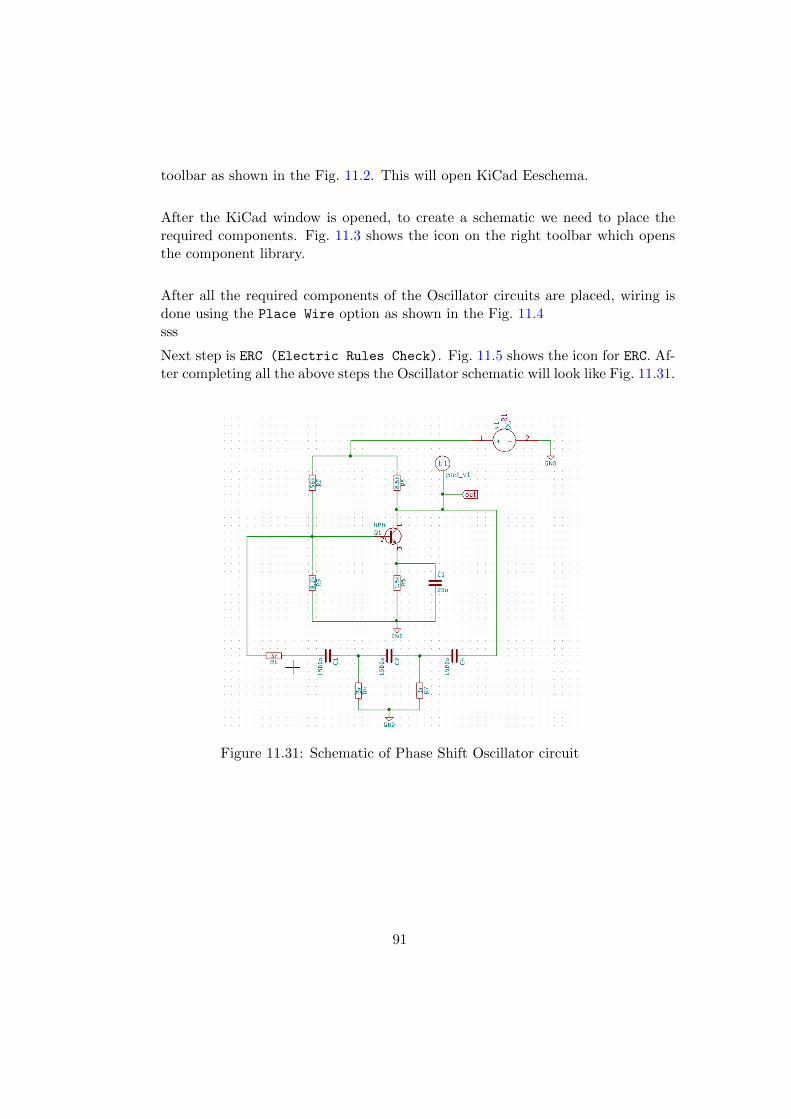
toolbar as shown in the Fig. 11.2. This will open KiCad Eeschema.
After the KiCad window is opened, to create a schematic we need to place therequired components. Fig. 11.3 shows the icon on the right toolbar which opensthe component library.
After all the required components of the Oscillator circuits are placed, wiring isdone using the Place Wire option as shown in the Fig. 11.4sss
Next step is ERC (Electric Rules Check). Fig. 11.5 shows the icon for ERC. Af-ter completing all the above steps the Oscillator schematic will look like Fig. 11.31.
Figure 11.31: Schematic of Phase Shift Oscillator circuit
91
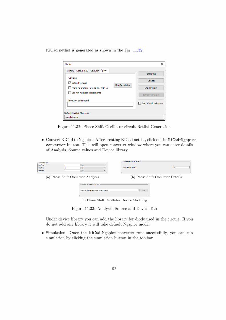
KiCad netlist is generated as shown in the Fig. 11.32
Figure 11.32: Phase Shift Oscillator circuit Netlist Generation
• Convert KiCad to Ngspice: After creating KiCad netlist, click on the KiCad-Ngspiceconverter button. This will open converter window where you can enter detailsof Analysis, Source values and Device library.
(a) Phase Shift Oscillator Analysis (b) Phase Shift Oscillator Details
(c) Phase Shift Oscillator Device Modeling
Figure 11.33: Analysis, Source and Device Tab
Under device library you can add the library for diode used in the circuit. If youdo not add any library it will take default Ngspice model.
• Simulation: Once the KiCad-Ngspice converter runs successfully, you can runsimulation by clicking the simulation button in the toolbar.
92
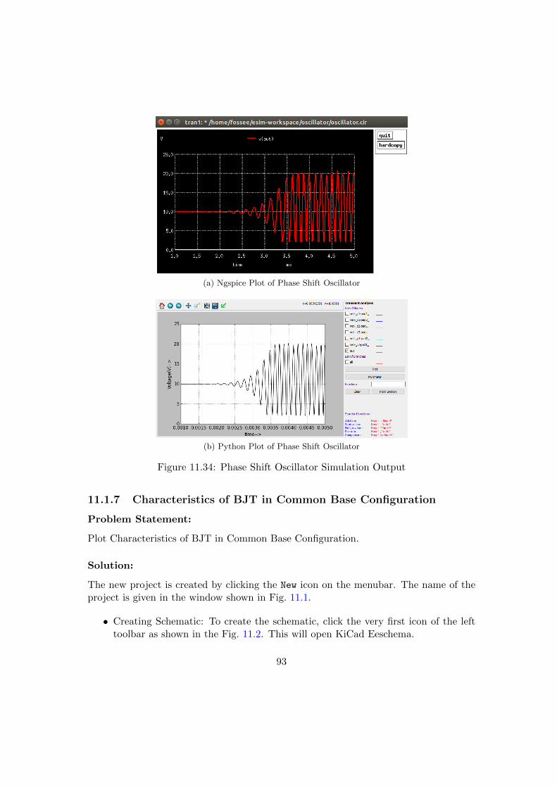
(a) Ngspice Plot of Phase Shift Oscillator
(b) Python Plot of Phase Shift Oscillator
Figure 11.34: Phase Shift Oscillator Simulation Output
11.1.7 Characteristics of BJT in Common Base Configuration
Problem Statement:
Plot Characteristics of BJT in Common Base Configuration.
Solution:
The new project is created by clicking the New icon on the menubar. The name of theproject is given in the window shown in Fig. 11.1.
• Creating Schematic: To create the schematic, click the very first icon of the lefttoolbar as shown in the Fig. 11.2. This will open KiCad Eeschema.
93
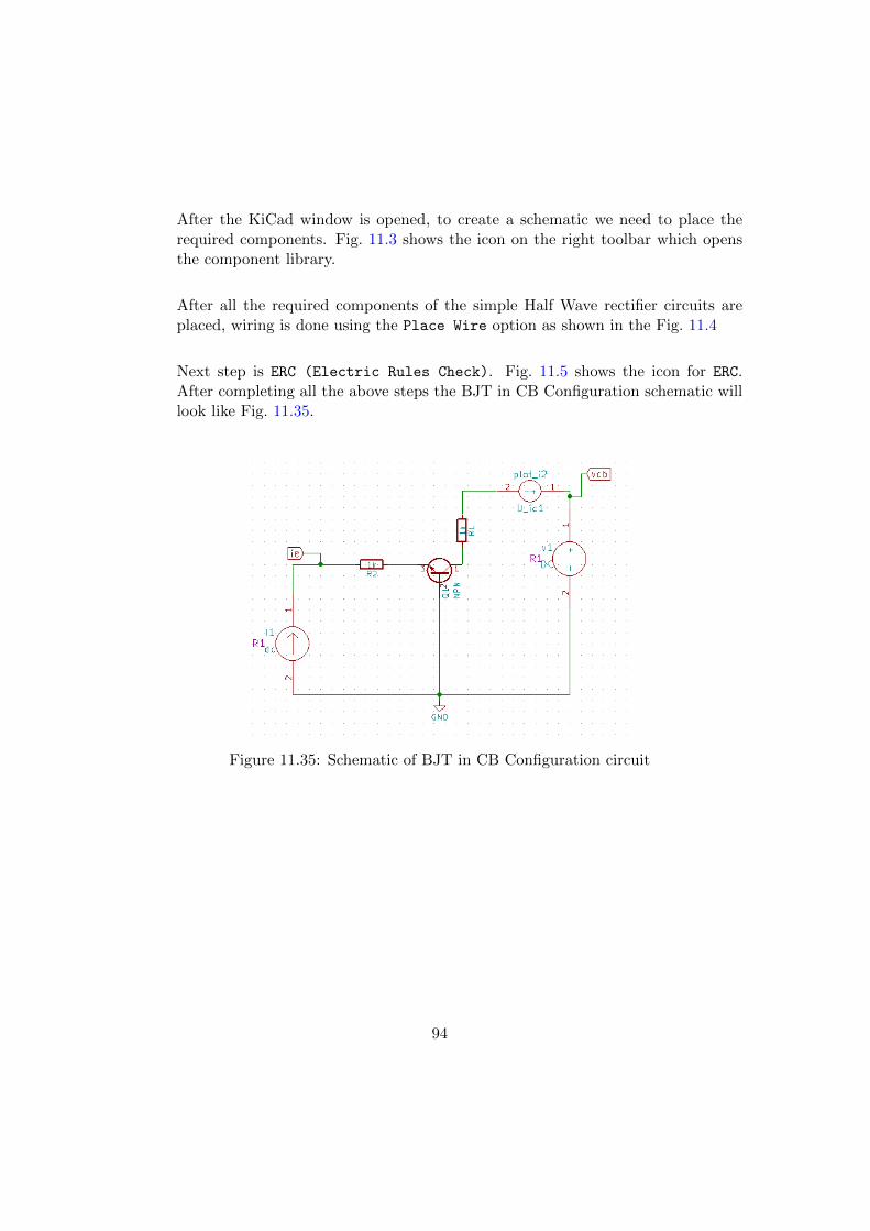
After the KiCad window is opened, to create a schematic we need to place therequired components. Fig. 11.3 shows the icon on the right toolbar which opensthe component library.
After all the required components of the simple Half Wave rectifier circuits areplaced, wiring is done using the Place Wire option as shown in the Fig. 11.4
Next step is ERC (Electric Rules Check). Fig. 11.5 shows the icon for ERC.After completing all the above steps the BJT in CB Configuration schematic willlook like Fig. 11.35.
Figure 11.35: Schematic of BJT in CB Configuration circuit
94

KiCad netlist is generated as shown in the Fig. 11.36
Figure 11.36: BJT in CB Configuration circuit Netlist Generation
• Convert KiCad to Ngspice: After creating KiCad netlist, click on the KiCad-Ngspiceconverter button. This will open converter window where you can enter detailsof Analysis, Source values and Device library.
(a) BJT in CB Configuration Analysis (b) BJT in CB Configuration Source Details
(c) BJT in CB Configuration Device Modeling
Figure 11.37: Analysis, Source and Device Tab
Under device library you can add the library for diode used in the circuit. If youdo not add any library it will take default Ngspice model.
• Simulation: Once the KiCad-Ngspice converter runs successfully, you can runsimulation by clicking the simulation button in the toolbar.
95

(a) Ngspice Plot of BJT in CB Configuration
(b) Python Plot of BJT in CB Configuration
Figure 11.38: BJT in CB Configuration Simulation Output
96

Chapter 12
PCB Design
Printed Circuit Board (PCB) design is an important step in electronic system design.Every component of the circuit needs to be placed and connections routed to minimisedelay and area. Each component has an associated footprint. Footprint refers to thephysical layout of a component that is required to mount it on the PCB. PCB designinvolves associating footprints to all components, placing them appropriately to min-imise wire length and area, connecting the footprints using tracks or vias and finallyextracting the required files needed for printing the PCB. Let us see the steps to designPCB using eSim.
12.1 Schematic creation for PCB design
In Chapter 5, we have seen the differences between schematic for simulation and schematicfor PCB design. Let us design a PCB Layout for a ’constant 5V DC supply’ circuitnamed as 7805VoltageRegulator. First, we will simulate the circuit. Refer to Fig. 12.1for the schematic used for simulation. After satisfying simulation results, we will moveto PCB design. For this, we will remove the Source(s), Probes (plot v , plot db etc.),and global labels connected solely for the purpose of viewing simulation plots conve-niently.Connectors are the physical components that are used to interface/connect the boardto external peripherals or sources.
12.1.1 Removing components required for simulation from the schematic
We will remove the components which were placed for simulation purpose only.
Components that will be placed on the board need to be added in the schematic.
Modify the circuit schematic as shown in Fig. 12.2. The two pin female connector(Conn 01x02 Female) is placed for the taking the 5V output supply meanwhile a 2 pin

Figure 12.1: Schematic for simulation of the constant 5V DC supply circuit
Figure 12.2: Schematic after adding connectors and removing the probes and sources.
Screw Terminal (Screw Terminal 01x02) is used to transmit the input signal on board.Do the annotation and test for ERC. Refer to Chapter 5 to know more about basicsteps in schematic creation.
12.1.2 Mapping of components using Cvpcb
Once the schematic for PCB Design is created, one needs to map each component inthe schematic to the appropriate footprint. The tool Cvpcb is used for this.
Cvpcb can be launched by clicking the icon Run Cvpcb to associate footprints
and components in Eeschema or by going under the Tools menu and selecting Assign
Component Footprint option.
12.1.3 Familiarising with Cvpcb Window
I. When one opens Cvpcb after annotating and running ERC on the schematic intendedfor PCB Design a window as shown in Fig. 12.3 will be obtained. The Toolbar for usingCvpcb will be available in the top-most left corner.
II. The left pane has a list of all footprint libraries in the database.
98
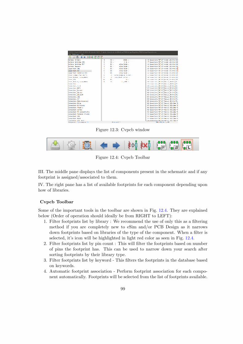
Figure 12.3: Cvpcb window
Figure 12.4: Cvpcb Toolbar
III. The middle pane displays the list of components present in the schematic and if anyfootprint is assigned/associated to them.
IV. The right pane has a list of available footprints for each component depending uponhow of libraries.
Cvpcb Toolbar
Some of the important tools in the toolbar are shown in Fig. 12.4. They are explainedbelow (Order of operation should ideally be from RIGHT to LEFT):
1. Filter footprints list by library : We recommend the use of only this as a filteringmethod if you are completely new to eSim and/or PCB Design as it narrowsdown footprints based on libraries of the type of the component. When a filter isselected, it’s icon will be highlighted in light red color as seen in Fig. 12.4.
2. Filter footprints list by pin count : This will filter the footprints based on numberof pins the footprint has. This can be used to narrow down your search aftersorting footprints by their library type.
3. Filter footprints list by keyword - This filters the footprints in the database basedon keywords.
4. Automatic footprint association - Perform footprint association for each compo-nent automatically. Footprints will be selected from the list of footprints available.
99

Note: This method of association is not recommended at all.5. Delete all associations - Delete all the footprint associations made. This will erase
all your association till now so be very careful in selecting this.6. Select next unlinked component: Using this you can go to the next component in
the list of components for associating a footprint.7. Select previous unlinked component: Using this you can go to the previous com-
ponent in the list of components for associating a footprint.8. View selected footprint - View the selected footprint in 2D. See Sec. 12.1.4 for
more details.Before clicking on this, make sure that a footprint is selected. Order of thisoperation should be1. Selection of footprint library from the left-most pane2. Selecting a footprint from the right-most pane3. Click on View selected footprint
9. Edit footprint library table - One should familiarize themselves with Cvpcb firstand then only choose to use this. This impacts the footprints that you can choose,so be careful before making any severe changes.
10. Save netlist and footprint files - Save the netlist and the footprints that are as-sociated with it. One ought to save the association after having assigned properfootprints to all the components.
12.1.4 Viewing footprints in 2D and 3D
To view a footprint in 2D, select the component for which you wish to view the availablefootprints, then select the library from left-most pane and now from the right pane andclick on the desired footprint and click on View selected footprint from the menubar. Let us view a footprint for C1 from the Capacitors THT footprint library. ChooseC1 from the middle pane as shown, click on Capacitors THT in the left-most pane andselect the View selected footprint tool. On clicking the View selected footprint tool,the Footprint window with the view in 2D will be displayed. 2D view of the footprintCP Radial D5.0mm P2.50mm is shown in Fig. 12.6.
Click on the 3D Display icon in the Footprint window, as shown in Fig. 12.6. A topview of the selected footprint in 3D is obtained. Click on the footprint and rotate itusing the computer mouse to get 3D views from various angles. One such view of thefootprint in 3D is shown in Fig. 12.7.
12.1.5 Mapping of components in the circuit
1. Click on C1 from the middle pane. Choose the footprint library Capacitors THTfrom the left pane and locate the footprint CP Radial D5.0mm P2.50mm. By doubleclicking on it, the said footprint will be assigned to C1.
100

Figure 12.5: Viewing footprint for C1
Figure 12.6: Footprint CP Radial D5.0mm P2.50mm’s view in 2D.
2. Similarly choose the footprints per Fig. 12.8 where the footprint association forall the footprints is shown in Fig. 12.8. Save the footprint association by click-ing on the Save footprint association in schematic component footprint
fields tool from the CvPcb toolbar..
101

Figure 12.7: 3D view of the footprint
Figure 12.8: Footprint mapping completed for the circuit
12.1.6 Netlist generation for PCB
1. After having saved your footprint association, switch back to the Eeschema win-dow and press Ctrl+S.
2. The netlist for PCB is different from that for simulation. To generate netlist forPCB, click on the Generate netlist tool from the top toolbar in Schematic editor.
3. In the Netlist window, under the tab Pcbnew, Select the option Default format.This is shown in Fig. 12.9. Click on Generate option.
102
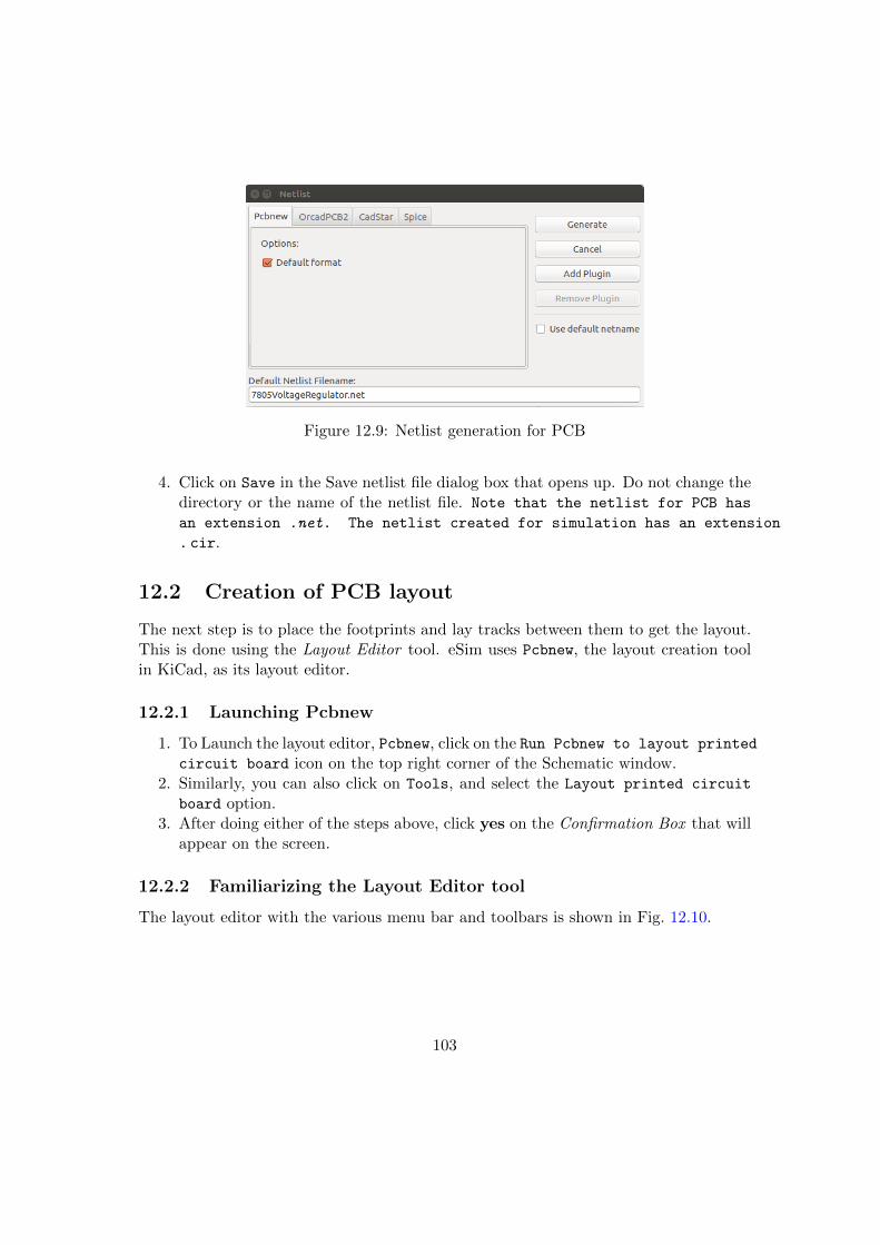
Figure 12.9: Netlist generation for PCB
4. Click on Save in the Save netlist file dialog box that opens up. Do not change thedirectory or the name of the netlist file. Note that the netlist for PCB has
an extension .net. The netlist created for simulation has an extension
. cir.
12.2 Creation of PCB layout
The next step is to place the footprints and lay tracks between them to get the layout.This is done using the Layout Editor tool. eSim uses Pcbnew, the layout creation toolin KiCad, as its layout editor.
12.2.1 Launching Pcbnew
1. To Launch the layout editor, Pcbnew, click on the Run Pcbnew to layout printed
circuit board icon on the top right corner of the Schematic window.2. Similarly, you can also click on Tools, and select the Layout printed circuit
board option.3. After doing either of the steps above, click yes on the Confirmation Box that will
appear on the screen.
12.2.2 Familiarizing the Layout Editor tool
The layout editor with the various menu bar and toolbars is shown in Fig. 12.10.
103
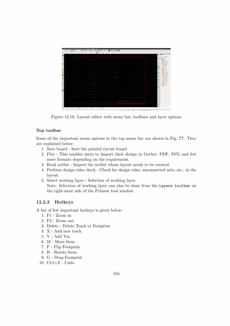
Figure 12.10: Layout editor with menu bar, toolbars and layer options
Top toolbar
Some of the important menu options in the top menu bar are shown in Fig. ??. Theyare explained below:
1. Save board - Save the printed circuit board2. Plot - This enables users to import their design in Gerber, PDF, SVG and few
more formats depending on the requirement.3. Read netlist - Import the netlist whose layout needs to be created.4. Perform design rules check - Check for design rules, unconnected nets, etc., in the
layout.5. Select working layer - Selection of working layer.
Note: Selection of working layer can also be done from the Layers toolbar onthe right-most side of the Pcbnew tool window.
12.2.3 Hotkeys
A list of few important hotkeys is given below:1. F1 - Zoom in2. F2 - Zoom out3. Delete - Delete Track or Footprint4. X - Add new track5. V - Add Via6. M - Move Item7. F - Flip Footprint8. R - Rotate Item9. G - Drag Footprint
10. Ctrl+Z - Undo
104

Figure 12.11: Default Hotkeys
11. E - Edit ItemThe entire list of Hotkeys can be viewed by selecting Preferences from the top menubar and choosing List Current Keys from the option Hotkeys.
12.2.4 Designing PCB layout for 7805VoltageRegulator circuit
Click on Read Netlist tool from the top toolbar of Pcbnew. Click on Browse Netlist fileson the Netlist window that opens up. Select the .net file that was modifiedafter assigning footprints. Click on Open. Now Click on Read Current Netlist on theNetlist window. The sequence of operations is shown in Fig. 12.12.
Arranging the footprints
1. After clicking on Read Netlist button and closing the Read Netlist window, thefootprints that we assigned will appear on the Pcbnew screen in a cluttered fashion,stacked on top of each other as shown in Fig. 12.13
2. Let us separate these footprints and place them in proper orientation per therequirement of the circuit. Let us start with Screw Terminal 01x02 footprint.
3. Right Click on the text Screw Terminal 01x02 in the Pcbnew window, and selectFootprint J1 on F.Cu. and select the Move option from the list.
4. The footprint will be glued to the cursor and it can be placed in the location ofone’s choice by moving the cursor at the desired location and clicking once toplace it there.
5. We have moved the Screw Terminal 01x02 footprint to the left side of the Pcbnewwindow.
6. Once again right click on the text Screw Terminal 01x02 in the Pcbnew window,
105
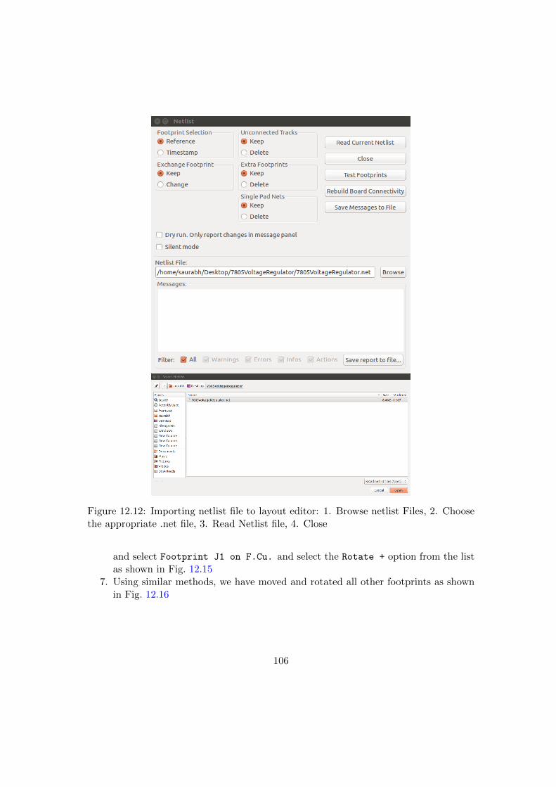
Figure 12.12: Importing netlist file to layout editor: 1. Browse netlist Files, 2. Choosethe appropriate .net file, 3. Read Netlist file, 4. Close
and select Footprint J1 on F.Cu. and select the Rotate + option from the listas shown in Fig. 12.15
7. Using similar methods, we have moved and rotated all other footprints as shownin Fig. 12.16
106

Figure 12.13: Cluttered footprints
Figure 12.14: Moving the footprint
Setting Design Rules
1. Click on Design Rules on top of the Pcbnew window, select Design Rules
option from the drop down menu there.
2. Design Rules Editor window will open, Under the Net Classes Editor, locatethe Track Width box, erase the default value from the window placed under theTrack Width box and enter 1.25 as the track width.
3. Click on Global Design Rules, under Minimum Allowed Values, locate Min
track width, erase the default value and enter 1.25 in the data entry field onthe right side of it as shown in Fig. 12.17. This will ensure that all tracks placedare of width 1.25mm and that when we perform Design Rules Check, the checks
107
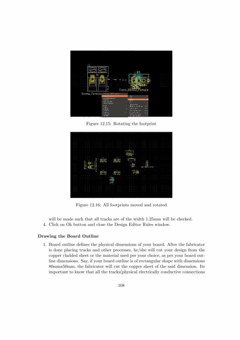
Figure 12.15: Rotating the footprint
Figure 12.16: All footprints moved and rotated
will be made such that all tracks are of the width 1.25mm will be checked.4. Click on Ok button and close the Design Editor Rules window.
Drawing the Board Outline
1. Board outline defines the physical dimensions of your board. After the fabricatoris done placing tracks and other processes, he/she will cut your design from thecopper cladded sheet or the material used per your choice, as per your board out-line dimensions. Say, if your board outline is of rectangular shape with dimensions80mmx50mm, the fabricator will cut the copper sheet of the said dimension. Itsimportant to know that all the tracks(physical electrically conductive connections
108
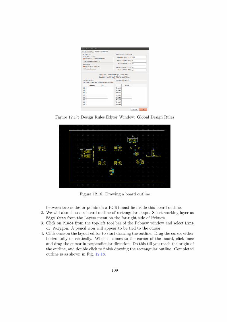
Figure 12.17: Design Rules Editor Window: Global Design Rules
Figure 12.18: Drawing a board outline
between two nodes or points on a PCB) must lie inside this board outline.2. We will also choose a board outline of rectangular shape. Select working layer as
Edge.Cuts from the Layers menu on the far-right side of Pcbnew.3. Click on Place from the top-left tool bar of the Pcbnew window and select Line
or Polygon. A pencil icon will appear to be tied to the cursor.4. Click once on the layout editor to start drawing the outline. Drag the cursor either
horizontally or vertically. When it comes to the corner of the board, click onceand drag the cursor in perpendicular direction. Do this till you reach the origin ofthe outline, and double click to finish drawing the rectangular outline. Completedoutline is as shown in Fig. 12.18.
109
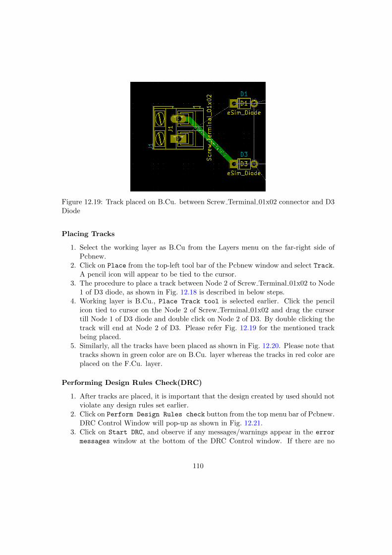
Figure 12.19: Track placed on B.Cu. between Screw Terminal 01x02 connector and D3Diode
Placing Tracks
1. Select the working layer as B.Cu from the Layers menu on the far-right side ofPcbnew.
2. Click on Place from the top-left tool bar of the Pcbnew window and select Track.A pencil icon will appear to be tied to the cursor.
3. The procedure to place a track between Node 2 of Screw Terminal 01x02 to Node1 of D3 diode, as shown in Fig. 12.18 is described in below steps.
4. Working layer is B.Cu., Place Track tool is selected earlier. Click the pencilicon tied to cursor on the Node 2 of Screw Terminal 01x02 and drag the cursortill Node 1 of D3 diode and double click on Node 2 of D3. By double clicking thetrack will end at Node 2 of D3. Please refer Fig. 12.19 for the mentioned trackbeing placed.
5. Similarly, all the tracks have been placed as shown in Fig. 12.20. Please note thattracks shown in green color are on B.Cu. layer whereas the tracks in red color areplaced on the F.Cu. layer.
Performing Design Rules Check(DRC)
1. After tracks are placed, it is important that the design created by used should notviolate any design rules set earlier.
2. Click on Perform Design Rules check button from the top menu bar of Pcbnew.DRC Control Window will pop-up as shown in Fig. 12.21.
3. Click on Start DRC, and observe if any messages/warnings appear in the error
messages window at the bottom of the DRC Control window. If there are no
110
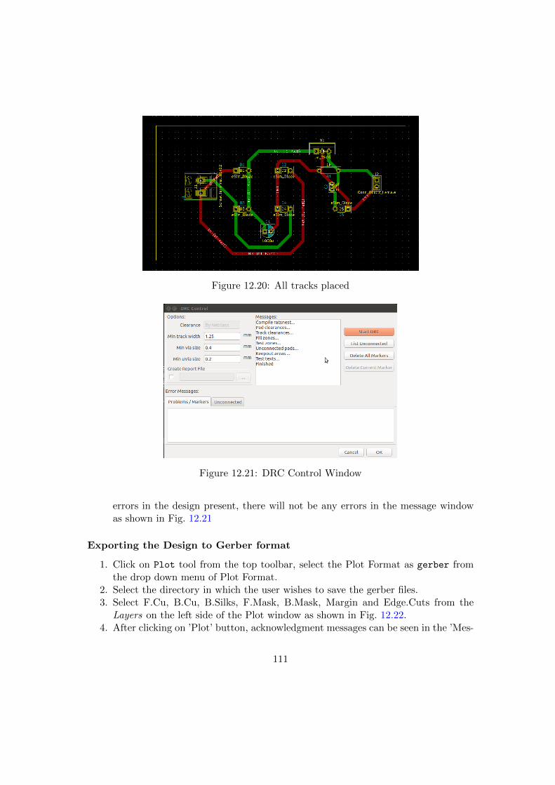
Figure 12.20: All tracks placed
Figure 12.21: DRC Control Window
errors in the design present, there will not be any errors in the message windowas shown in Fig. 12.21
Exporting the Design to Gerber format
1. Click on Plot tool from the top toolbar, select the Plot Format as gerber fromthe drop down menu of Plot Format.
2. Select the directory in which the user wishes to save the gerber files.3. Select F.Cu, B.Cu, B.Silks, F.Mask, B.Mask, Margin and Edge.Cuts from the
Layers on the left side of the Plot window as shown in Fig. 12.22.4. After clicking on ’Plot’ button, acknowledgment messages can be seen in the ’Mes-
111
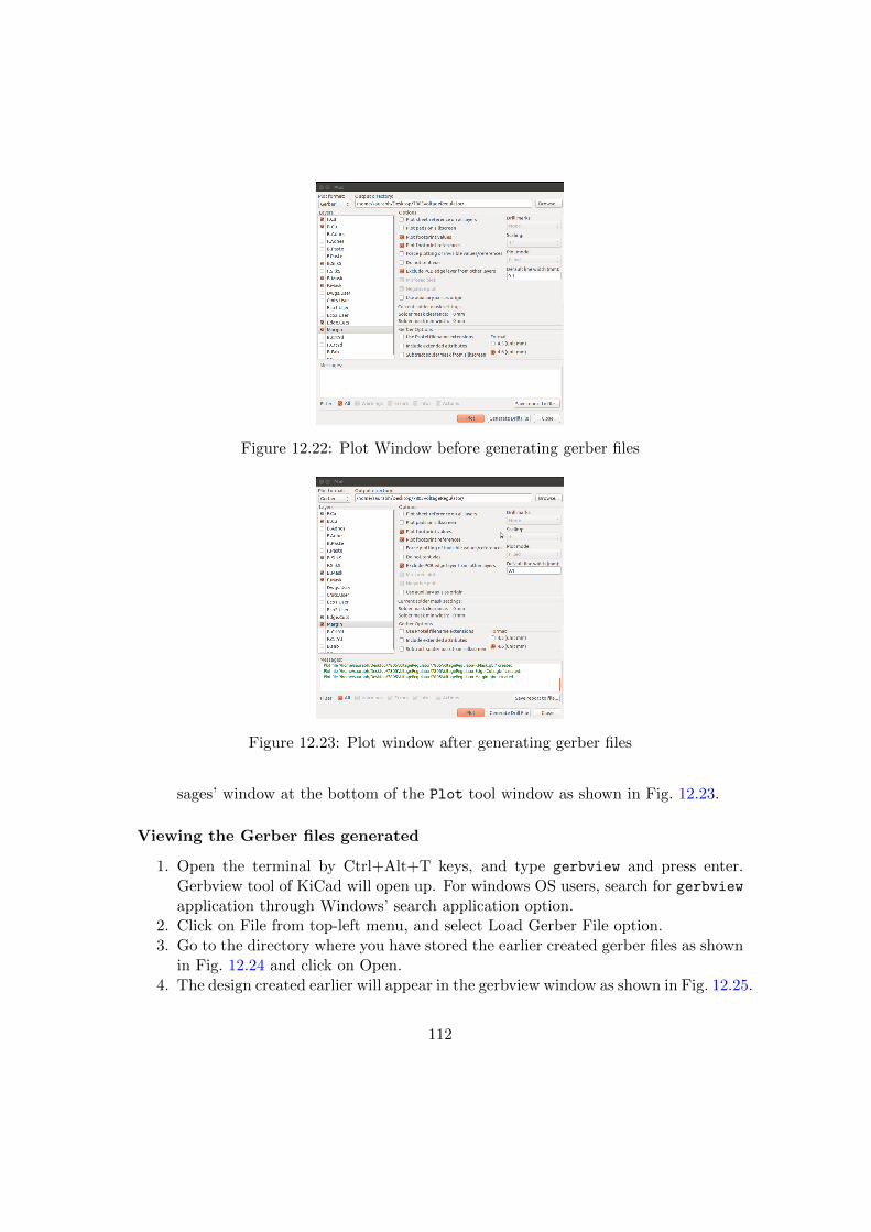
Figure 12.22: Plot Window before generating gerber files
Figure 12.23: Plot window after generating gerber files
sages’ window at the bottom of the Plot tool window as shown in Fig. 12.23.
Viewing the Gerber files generated
1. Open the terminal by Ctrl+Alt+T keys, and type gerbview and press enter.Gerbview tool of KiCad will open up. For windows OS users, search for gerbviewapplication through Windows’ search application option.
2. Click on File from top-left menu, and select Load Gerber File option.3. Go to the directory where you have stored the earlier created gerber files as shown
in Fig. 12.24 and click on Open.4. The design created earlier will appear in the gerbview window as shown in Fig. 12.25.
112
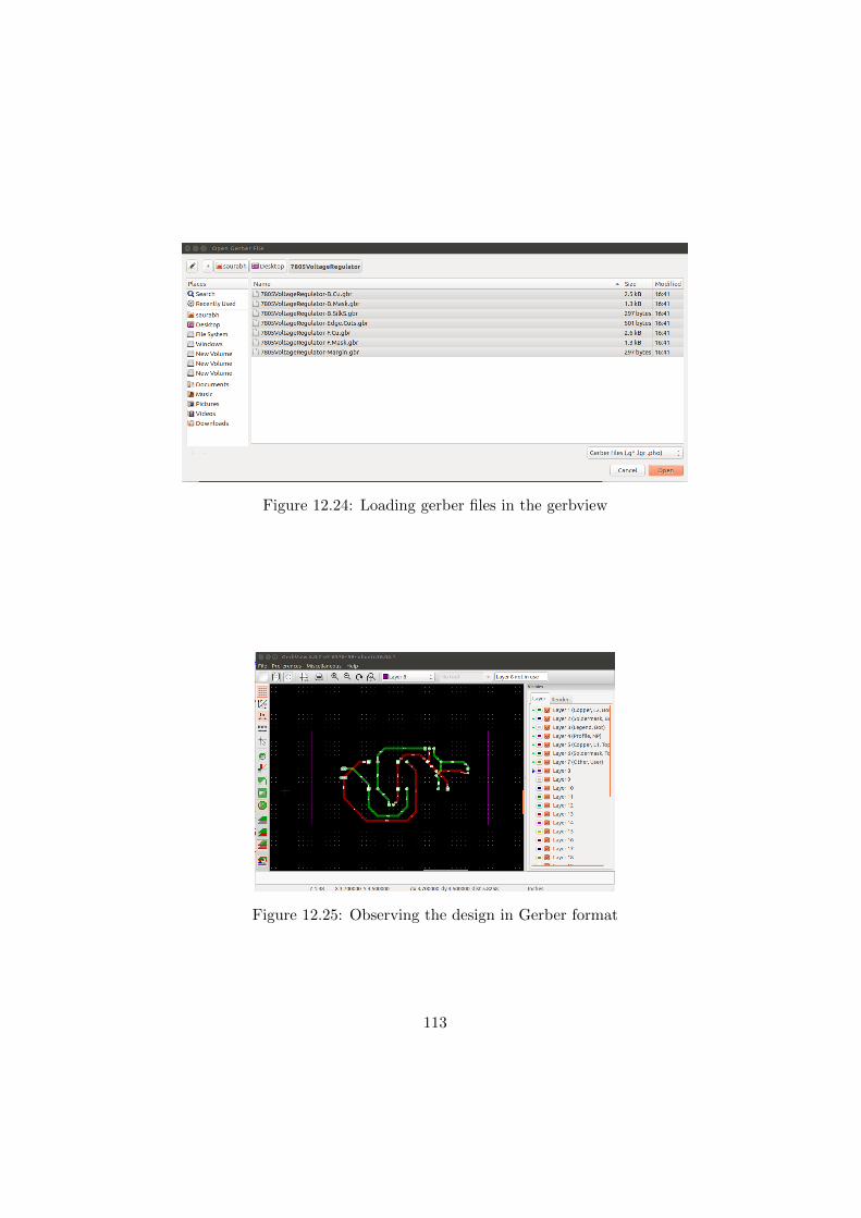
Figure 12.24: Loading gerber files in the gerbview
Figure 12.25: Observing the design in Gerber format
113

Chapter 13
Appendix
13.1 Appendix A
13.1.1 Backing up important data before uninstalling eSim
Locate the folders : SubcircuitLibrary and deviceModelLibrary in the eSim instal-lation directory, compress them in .zip or .rar format on your Desktop or some otherlocation which does not contain eSim related files.
The projects created and stored in eSim-Workspace will not be deleted when one unin-stalls eSim, hence there is no need to backup these project files.
Newly created subcircuits and device models should be backed up as explained above.A way to take backup of the subcircuit blocks (external outlook) which appears in theschematic editor (not to be confused with internal circuit of the subcircuit) is explainedin the Subcircuit section of this manual.
13.1.2 Uninstalling eSim
For Windows OS users
Locate the uninstaller "uninst-eSim.exe" from the directory where eSim is present,by default it is installed at C:/FOSSEE/eSim/
Run the uninstaller executable and all the eSim related files and components exceptthe projects created in eSim-Workspace will be deleted.
For Ubuntu Linux OS users
Open terminal and go to the location where eSim is stored using the cd command.
type the following and press enter :$ ./install-eSim.sh --uninstall
114

13.2 Appendix B
13.2.1 Pin types in KiCad
• Input: is a unidirectional input.
• Output: is a unidirectional output that can drive high or low.
• Bidirectional:can act as an input or an output. The I/O pins on microcontrollersare bidirectional.
• Tri-state:is an output that can drive high or low, but can also be placed in ahigh-impedance state where it floats. The 74125 is a chip with tri-state outputs(sometimes called three-state outputs: high, low, and high-impedance).
• Passive:is an unpowered connection, like resistors, capacitors and inductors.
• Unspecified: is, unspecified. User would use that when no other classificationfits.
• Power input: is a pin where power comes in to a chip. Both the VCC and GNDpins of chips would be classified as power inputs.
• Power outputs: are where power comes out of a chip. The outputs of voltageregulators are the most common example of this pin type.
• Open collector output pins: are outputs that can be driven low, but floatotherwise. These are good for wired-AND connections where the output goes lowif any of the attached open-collector pins goes low, but the output is pulled highby a pull-up resistor if all the pins are floating. The 7401 is a NAND gate chipwith open-collector outputs.
• Open emitter output pins: can be driven high, but float otherwise. These aregood for wired-OR connections where the output goes high if any of the attachedopen-emitter pins goes high, but the output is pulled low by a pull-down resistorif all the pins are floating.
• Not-connected:pins are pins which have no function. Think of these as packagepins that are not bonded to the IC inside.
13.2.2 ERC Table
• User can actually decide what you want to be told about, by setting the tablebelow accordingly.For instance if the user wanted the ERC to throw an error ifan input was connected to an input then the user would change the topmost boxfrom green (no message) to yellow (warning) or red (error) as shown in Fig. ??
115

Figure 13.1: ERC Table
13.3 Appendix C
13.3.1 Shortcut keys in Schematic editor
• Open the schematic editor and press Shift and ? keys simultaneously. This willdisplay the total shortcut keys, also called as Hotkeys. Please note that, if theshortcut key is related to a component, for example, changing its value or itsorientation etc, then your cursor must be located on that component.
• V: This edits the Component’s value.
• R: This rotates a component.
• A: This calls the place component tool through which you can add componentsin your schematic.
• M: This moves a component. After pressing M key, the component you chose willbe tied to the cursor and you can place it anywhere in the schematic by clickingonce on the schematic editor.
116

• C: This copies a component. After pressing C key, the component you chose willbe tied to the cursor and you can place it anywhere in the schematic by clickingonce on the schematic editor.
• Ctrl + H: This is to create a Global label. After pressing Ctrl + H keys simulta-neously, the global label will be tied to the cursor and you can place it anywherein the schematic by clicking once on the schematic editor.
• W: This calls the place wire tool through which you can add components in yourschematic.
13.3.2 Shortcut keys in PCB editor
• The shortcuts that can be used in the Pcbnew Layout Editor .Open the PcbnewLayout editor and press Shift and ? keys simultaneously.
• X: This calls the Place Track tool.
• R: This rotates a component.
• B: Fill or Refill All Zones.
13.4 Appendix D: ERC errors
• ErrType(1): Duplicate sheet names within a given sheet. Review sheet namesin hierarchy and remove duplicates.
• ErrType(2): Pin not connected and no No Connect Symbol. Check the pin andwire overlaps or place No connect symbol if pin should be left unconnected.
• ErrType(3): Pin connected to some others pins but no pin to drive it. Thismeans there is a power input pin and there is no power connected to the pin. Thisis typically solved by adding a PWR FLAG symbol to the schematic.
• ErrType(4): Conflict problem between pins. Severity: warning. Two pins con-nected but their function needs complementary signals (for ex. input -¿ output).You can have many power input pins connected to power output but no two poweroutput pins should be connected together.
• ErrType(5): Conflict Problem between pins, Severity: Error. This is becauseyou can only have one output or power output on the same net.
• ErrType(6): Mismatch between hierarchical labels and pins sheets. There isa mismatch between hierarchical label and existing pin sheet, try to re-importhierarchical pins to replace wrong pin sheet.
117

• ErrType(7): A no connect symbol is connected to more than 1 pin. ”No connect”symbol should be put at the end of the pin,and this pin should be left unconnectedat all costs.
• ErrType(8): Global label not connected to any other global label. There is aglobal label which has no pair in other sheet(s).
• ErrType(9): Two labels are equal for case insensitive comparisons Review schematiclabels to find possible duplicates, watch for similarity of large and small letters.
• ErrType(10): Two global labels are equal for case insensitive comparisons. Re-view global labels in hierarchy to find possible duplicates, watch for similarity oflarge and small letters.
118

13.5 Appendix E: Checks to be done before Simulation inNGHDL
1. VHDL filename should be in small letters without any space or special characters(Underscore is allowed).
2. Entity name, architecture declaration and the VHDL file name should matchexactly.
3. Declaration of each port should be done on a new line. See nghdl/Example/for further reference.
4. Port declaration can be either std logic or std logic vector. No other declara-tions are allowed.
5. All in ports should be declared before out ports.6. Maximum number of output ports that a VHDL entity under simulation can have
is 64, provided the port names are not too lengthy to overflow the buffer.7. Be extremely careful while dealing with Arithmetic Operations.
(See nghdl/Example/counter/counter.vhdl for further reference)8. If structural style is used, then the main entity of your VHDL code which is to be
simulated, should be declared first in the file with inclusion of libraries for subse-quent declaration of each supporting entity. See nghdl/Example/full adder/full adder structural.vhdl for further reference.
9. Do not use sudo or root permissions while working Mixed-Mode Simulation andeSim.
10. If there are more than one VHDL file to be uploaded, then do it one-by-one, asdescribed below:(a) Click on NGHDL button on eSim or type nghdl/ in terminal. A new window
will be opened.(b) Upload your first VHDL file and wait for the process to be completed.(c) Check if there are any Errors on the console. If possible, try to debug it and
report your error and its solution to us. Otherwise, you can send the errorto us. If there are no errors, upload your second model and repeat the stepsmentioned above.You can upload as many models as required.
11. Do not upload two or more VHDL files simultaneously :Add files option allow you to use a smaller entity / subpart / submodule to sup-port the main VHDL file. That is, a digital model will be generated correspondingto that file that has been browsed. The file that has been added to Nghdl uploadwindow will only be placed along with the model under model’s DUTghdl folderto support the model.Hence, browsing one file and adding several files won’t create that many numbermodels, but only model will be created corresponding to the browsed file.
12. Maximum number of NGHDL models that can be simulated at once is restricted
119

to 512.13. Next simulation should be started only after the completion of the previous/current
simulation. No two simulations should be executed at once.14. While providing parameters to the adc-dac bridges that correspond to any NGHDL
model, make sure that the rise and fall delays of ADC and DAC bridges arecomparable to the simulation time parameters passed. Some examples are givenbelow:
(a) Circuits involving both Analog and NGHDL Components - If steptime is 10 ms and simulation time is 200 ms, then DAC-ADC delays shouldbe atleast 1 us.
(b) Circuits involving only NGHDL Components - If step time is 10 msand simulation time is 200 ms, then DAC-ADC delays should be atleast 500us.
(c) inverter subcircuit [INVCMOS] has a delay of 6 ms(can be changed by chang-ing capacitor value inside the CMOS subcircuit). NGHDL model created,ADC and DAC bridges has rise and fall time 1 ns. You are simulating thiscircuit for 100 ms, it won’t work. Increase the rise and fall delay for theADC-DAC models from 1 nanosecond to 1 microsecond (1/1000th of theanalog delay).
In general (a thumb rule to follow), delay value can be set to at least 1/500thpart of the stop time.
15. If there is a need to use multiple instances of same NGHDL model in a givenproject and if even one of these instances need to have a different parametervalue than the rest of the instances, then a separate NGHDL model needs to begenerated with a different name.
120

13.6 Appendix F: Common Errors in NGHDL
Before concluding anything about NGHDL’s working or about eSim’s Mixed-Mode Sim-ulation, do check the console for outputs and logs. Kindly see the following errors onUser’s end that can be rectified there itself :
13.6.1 NGHDL Upload Errors
• Error while opening NGHDL. Please make sure NGHDL is installed :
As the error indicates, NGHDL is not installed at all or there has been some errorduring installation which was not resolved effectively. However, if the installationwas done correctly, then open a terminal and type :
$ sudo ln -s <your path to nghdl>/nghdl/src/ngspice ghdl.py /usr/loc
al/bin/nghdl
Now type nghdl in terminal and check if the NGHDL Digital Model Creator
window opens or not.
• Error - select a *.vhdl file :This type of error can occur due to a variety of underlying user issues. Checkterminal from which eSim is launched for more detailed errors. However, followingis a list of common mistakes that a user may face :
– Permission Denied - Change the permission of ngspice-nghdl folder re-cursively to be used by all the users. To do so, open a terminal and type:
$ sudo chown $USER:$USER -R $HOME/ngspice-nghdl/
13.6.2 Simulation Related Errors
• GHDL compilation error :The VHDL code itself is incorrect, as a result the corresponding model generatedis incorrect and no simulation will be done. Kindly upload a correct VHDL code.
• Warning : There is an ’U’|’X’|’W’|’Z’|’-’ in an arithmetic operand, theresult will be ’X’(es) :Such warnings are difficult to find in xterm outputs. However, it indicates thatthere is some logical error in your VHDL code regarding the data types / arith-metic operations / type conversions, etc. Kindly upload a logically correct VHDLcode.
• Unknown model name 〈your nghdl model〉 - Ngspice :If this error occurs on xterm window while simulating with Ngspice, then check
121

whether the Ngspice engine used is of system built or that of the NGHDL. Tocheck the same, follow the steps:
1. Open terminal and type : $ whereis ngspice
2. Go to the location where ngspice executable is found.
3. Now, check if this ngspice is a link to:ngspice-nghdl/install dir/bin/ngspice
4. If it is not a link, then uninstall the system’s installed ngspice and create alink to the above mentioned path by typing the command in terminal as:
$ sudo ln -s $HOME/ngspice-nghdl/install dir/bin/ngspice/<previo
us ngpsice location>/ngspice
5. If output of step 1 is empty, then run above command by replacing<previous ngpsice location> with /usr/bin
• Unknown model name 〈your nghdl model〉 - KiCad-to-Ngspice :
If this error occurs during KiCad-to-Ngspice conversion, then check whether theuploaded VHDL file had any Uppercase characters or any other special charactersin its filename. Note that only lowercase characters and underscores are allowed.
• Warning : component instance uut of xyz is not bound :
This logical error is related to the VHDL code which is shown as a Warning andsimulation plots may also appear. However, these plots are incorrect as the VHDLmodel itself is incorrect. Following are the examples that can cause this error:
– If a vhdl file is saved as dummycode.vhdl and the entity and architecture aredeclared as for example, codedummy or dummy or something other than thename of the actual vhdl file itself, one will get the above error.
– If structural style is being used and above error is seen, then kindly makethe necessary changes by referring our example found at:nghdl/Example/full adder/full adder structural.vhdl
Kindly check with the GHDL documentation and online resources too are availableregarding this GHDL error.
• Warning : Too many analog/event-driven solution alternationsWarning : Convergence problems at node (net-*).. . . . . . . . . . . . . . . . . . . . . . . . . . . .Transient solution failed -doAnalyses: iteration limit reached :
As the error says itself that if too many analog components are connected todigital model due to which there can be many analog alternations (or if too many
122

events are generated rapidly due to which the convergence would fail for thosemodels), then the initial conditions won’t converge and the transient solution willfail. Follow these steps to resolve it:
1. Open the corresponding project’s cir.out file (\*.cir.out").
2. Just below the “.control” statement and above the “run” statement, inserta new line.
3. On this new line, type “option noopalter”.
4. Save the file and exit.
5. Run the simulation once again.
• doAnalyses: TRAN : Timestep too small; time = ... , timestep = . . . ;trouble with node ... run simulation(s) aborted :
As the error says :
– Check if the time-step is too small as compared to the stop-time.
– If the time-step is of the same order(scalable) as that of the stop-time, thencheck the delays of the adc-dac bridges and make them comparable to simu-lation stop-time.
– If the delays are comparable, then check the parameters provided to thedigital and analog models and set them appropriately.
• chmod : changing permissions of ‘any file’: Operation not permitted :
This error, displayed on xterm by Ngspice, is similar to that of Permission
Denied error. Kindly refer section 13.4.1 for the same.
13.6.3 Model Deletion
If you want to delete a model from your file system or is deleted due to unavoidablecircumstances, perform the following steps (to ensure consistency within the software) :
1. Delete the folders found at path :
– ngspice-nghdl/src/xspice/icm/ghdl/<your model>/
– ngspice-nghdl/release/src/xspice/icm/ghdl/<your model>/
2. Delete the name and description of that model from the files :
– ngspice-nghdl/src/xspice/icm/ghdl/modpath.lst
– eSim Nghdl.lib
Realign the content of these files by removing any extra spaces or empty linesfound between any two subsequent remaining model names after deletion.
3. Delete the file found at path :eSim-version/src/modelParamXML/Nghdl/<your model>.xml
123

13.7 Appendix G: References
1 A. S. Sedra and K. C. Smith, Microelectronic Circuits - Theory and Applications.Oxford University Press, 2009.
2 K. M. Moudgalya, “Spoken Tutorial: A Collaborative and Scalable EducationTechnology,” CSI Communications, vol. 35, no. 6, pp. 10–12, September 2011,available at https://spoken-tutorial.org/CSI.pdf.
3 (2020, March). [Online]. Available: https://www.scilab.org/
4 (2020, March). [Online]. Available: https://scilab-test.garudaindia.in/scilab in/https://scilab-test.garudaindia.in/cloud
6 K. Kannan and K. Narayanan, “Ict-enabled scalable workshops for engineering col-lege teachers in india,” in Post-Secondary Education and Technology: A GlobalPerspective on Opportunities and Obstacles to Development (International andDevelopment Education), R. Clohey, S. Austin-Li, and J. C. Weldman, Eds. Pal-grave Macmillan, 2012.
7 (2020, March). [Online]. Available: https://esim.fossee.in
8 (2020, March). [Online]. Available: http://www.aakashlabs.org/
9 (2020, March). [Online].Available: http://en.wikipedia.org/wiki/Electronic design automation
10 (2020, March) Synaptic Package Manager Spoken Tutorial. [Online]. Available:https://www.spoken-tutorial.org/tutorial-search/?search foss=Linuxsearch language=English
11 (2020, March). [Online]. Available: https://www.kicad-pcb.org/
12 (2020, March). [Online]. Available: ngspice.sourceforge.net/
13 (2020, March). [Online]. Available: http://scilab.in/
14 S. M. Sandler and C. Hymowitz, SPICE Circuit Handbook. New York: McGraw-Hill Professional, 2006.
15 J.-P. Charras and F. Tappero. (2020, March). [Online]. Available: https://docs.kicad-pcb.org/
16 Wayne Stambaugh (2020, March). [Online].Available: https://launchpad.net/kicad/4.0/4.0.7
17 P. Nenzi and H. Vogt. (2020) Ngspice users manual version 31. [Online].Available: http://ngspice.sourceforge.net/docs/ngspice-manual.pdf
124

18 K. M. Moudgalya, “LATEX Training through Spoken Tutorials,” TUGboat, vol.32, no. 3, pp. 251–257, 2011.
19 (2020, March). [Online]. Available: https://www.spoken-tutorial.org/
125