Embed Size (px)
Citation preview

Notice
Hewlett-Packard to Agilent Technologies TransitionThis manual may contain references to HP or Hewlett-Packard. Please note that Hewlett-Packard’s former test and measurement, semiconductor products and chemical analysis businesses are now part of Agilent Technologies. To reduce potential confusion, the only change to product numbers and names has been in the company name prefix: where a product name/number was HP XXXX the current name/number is now Agilent XXXX. For example, model number HP8648 is now model number Agilent 8648.The material contained in this document is provided “as is,” and is subject to being changed, without notice, in future editions. Further, to the maximum extent permitted by applicable law, Agilent disclaims all warranties, either express or implied, with regard to this manual and any information contained herein, including but not limited to the implied warranties of merchantability and fitness for a particular purpose. Agilent shall not be liable for errors or for incidental or consequential damages in connection with the furnishing, use, or performance of this document or of any information contained herein. Should Agilent and the user have a separate written agreement with warranty terms covering the material in this document that conflict with these terms, the warranty terms in the separate agreement shall control.
To contact Agilent Technologies please use the information below;
Online assistance: http://www.agilent.com/find/assist
Americas
Canada 1 877 894 4414 Latin America (305) 269 7500 United States 1 800 829 4444
Asia Pacific
Australia 1 800 629 485 China 800 810 0189 Hong Kong 800 938 693
India 1 800 112 929 Japan 0 120 (421) 345 Korea 080 769 0800
Malaysia 1 800 888 848 Singapore 1 800 375 8100 Taiwan 0800 047 866
Thailand 1 800226 008
Europe & Middle East
Austria 43 (0) 1 360 277 1571 Belgium 32 (0) 2 404 93 40 Denmark 45 70 13 15 15
Finland 358 (0) 10 855 2100 France 0825 010 700* *0.125 Euros/minute
Germany 49 (0) 7031 464 6333
Ireland 1890 924 204 Israel 972-3-9288-504/544 Italy 39 02 92 60 8484
Netherlands 31 (0) 20 547 2111
Spain 34 (91) 631 3300
Sweden 0200-88 22 55
Switzerland 0800 80 53 53 United Kingdom 44 (0) 118 9276201
Other European Countries: http://www.agilent.com/find/contactus

Service Guide
Agilent ESG-D Series Signal Generators
Serial Number Prefixes:
ESG-D1000A, US3723 and belowESG-D2000A, US3723 and belowESG-D3000A, US3723 and belowESG-D4000A, US3723 and below
Part No. E4400-90014
Printed in USAPrint Date: July 1997
Copyright Hewlett-Packard Company 1997. All Rights Reserved. Reproduction, adaptation, or translation without prior written permission is prohibited, except as allowed under the copyright laws.
1400 Fountaingrove Parkway, Santa Rosa, CA 95403-1799, USA

ii

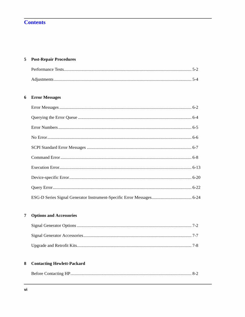
Contents
1 Initial Troubleshooting and Overall Block Diagram
Before You Begin Troubleshooting ......................................................................................... 1-2
Using this Service Guide to Troubleshoot ............................................................................... 1-3
Equipment Required for Troubleshooting ............................................................................... 1-4
Initial Troubleshooting............................................................................................................. 1-5
Overall Block Diagram............................................................................................................1-17
Overall Block Diagram (Option 1EH)..................................................................................... 1-19
Overall Block Diagram (Options UN3 & UN4)...................................................................... 1-21
2 Assembly-Level Troubleshooting with Block Diagrams
Before You Begin Troubleshooting ......................................................................................... 2-2
Using the Procedures in this Chapter....................................................................................... 2-3
A9 Output Board...................................................................................................................... 2-5
A9 Output Board Block Diagram ............................................................................................ 2-7
A11 Reference Board .............................................................................................................. 2-9
A11 Reference Board Block Diagram..................................................................................... 2-11
A12 Synthesizer/Doubler Board.............................................................................................. 2-13
A12 Synthesizer/Doubler Board Block Diagram .................................................................... 2-15
A14 CPU/Motherboard............................................................................................................2-17
A14 CPU/Motherboard Block Diagram (1 of 2) ..................................................................... 2-19
A14 CPU/Motherboard Block Diagram (2 of 2) ..................................................................... 2-21
AT1 Attenuator/RPP Block Diagram....................................................................................... 2-23
iii

Contents
A7 Baseband Generator Board Block Diagram (Option 1EH) ............................................... 2-25
A7 Baseband Generator Board Block Diagram (Options UN3 & UN4) ................................ 2-27
A8 Data Generator Board Block Diagram (Options UN3 & UN4) ........................................ 2-29
Interconnects Block Diagram - Power Supply and Ground (1 of 2) ....................................... 2-31
Interconnects Block Diagram - Power Supply and Ground (2 of 2) ....................................... 2-33
Interconnects Block Diagram - Modulation and Signal (1 of 2) ............................................. 2-35
Interconnects Block Diagram - Modulation and Signal (2 of 2) ............................................. 2-37
3 Replaceable Parts
Ordering Information............................................................................................................... 3-2
Save Money with Rebuilt-Exchange Assemblies.................................................................... 3-4
Abbreviations Used in Part Descriptions................................................................................. 3-6
Major Assemblies.................................................................................................................... 3-8
Cables ...................................................................................................................................... 3-16
Hardware and Other Instrument Parts ..................................................................................... 3-34
Miscellaneous .......................................................................................................................... 3-56
4 Assembly Replacement
Before You Replace an Assembly ........................................................................................... 4-2
Assemblies That You Can Replace.......................................................................................... 4-3
Instrument Cover ..................................................................................................................... 4-4
Front Panel............................................................................................................................... 4-6
Front Panel (Option 1EM)....................................................................................................... 4-10
iv

Contents
Rear Panel ................................................................................................................................ 4-14
Rear Panel (Option 1EM) ........................................................................................................ 4-18
A1 Front Panel Board .............................................................................................................. 4-22
A2 Display ............................................................................................................................... 4-24
A2DS1 Fluorescent Lamp ....................................................................................................... 4-26
A3 Inverter ............................................................................................................................... 4-28
A4 Power Supply .....................................................................................................................4-30
A4 Power Supply (Option 1EM) ............................................................................................. 4-34
A7 Baseband Generator Board (Option 1EH) ......................................................................... 4-38
A7 Baseband Generator Board (Options UN3 & UN4) .......................................................... 4-40
A8 Data Generator Board (Options UN3 & UN4) .................................................................. 4-42
A9, A11, and A12 Daughterboard Card Cage Boards............................................................. 4-44
A14 CPU/Motherboard............................................................................................................4-46
A14BT1 Battery....................................................................................................................... 4-50
A15 Daughterboard ................................................................................................................. 4-52
A16 Line Module..................................................................................................................... 4-56
A17 Rear Panel Interface Board (Options 1EH, UN3, UN4) .................................................. 4-58
AT1 Electronic Attenuator/RPP............................................................................................... 4-60
B1 Small Fan Assembly .......................................................................................................... 4-62
B2 Large Fan Assembly .......................................................................................................... 4-64
W11, W12, and W14 Semi-Rigid Cables................................................................................ 4-66
v
Contents
5 Post-Repair Procedures
Performance Tests.................................................................................................................... 5-2
Adjustments............................................................................................................................. 5-4
6 Error Messages
Error Messages ........................................................................................................................ 6-2
Querying the Error Queue ....................................................................................................... 6-4
Error Numbers ......................................................................................................................... 6-5
No Error................................................................................................................................... 6-6
SCPI Standard Error Messages ............................................................................................... 6-7
Command Error ....................................................................................................................... 6-8
Execution Error........................................................................................................................ 6-13
Device-specific Error............................................................................................................... 6-20
Query Error.............................................................................................................................. 6-22
ESG-D Series Signal Generator Instrument-Specific Error Messages.................................... 6-24
7 Options and Accessories
Signal Generator Options ........................................................................................................ 7-2
Signal Generator Accessories.................................................................................................. 7-7
Upgrade and Retrofit Kits........................................................................................................ 7-8
8 Contacting Hewlett-Packard
Before Contacting HP.............................................................................................................. 8-2
vi

Contents
Calling HP Sales and Service Offices...................................................................................... 8-3
Returning Your Signal Generator for Service.......................................................................... 8-5
Blue Repair Tags...................................................................................................................... 8-7
9 Safety and Regulatory
Safety Notes............................................................................................................................. 9-2
General Safety Considerations ................................................................................................ 9-3
Lithium Battery Disposal......................................................................................................... 9-4
Warranty................................................................................................................................... 9-5
Assistance ................................................................................................................................ 9-6
Notice....................................................................................................................................... 9-7
Certification ............................................................................................................................. 9-8
Index
vii

Contents
viii

1 Initial Troubleshooting and Overall Block Diagram
This chapter will help you begin troubleshooting your signal generator. The procedures in this chapter primarily check your instrument for failures that affect the power supplies or CPU function. An overall block diagram of your signal generator is at the end of this chapter.
1-1

Initial Troubleshooting and Overall Block DiagramBefore You Begin Troubleshooting
Before You Begin Troubleshooting
Avoid Personal Injury
WARNING: These servicing instructions are for use by qualified personal only. To avoid electrical shock, do not perform any servicing unless you are qualified to do so.
WARNING: The opening of covers or removal of parts is likely to expose dangerous voltages. Disconnect the product from all voltage sources while it is being opened.
WARNING: The detachable power cord is the instrument disconnecting device. It disconnects the mains circuits from the mains supply before other parts of the instrument. The front panel switch is only a standby switch and is not a LINE switch.
WARNING: The power cord is connected to internal capacitors that may remain live for 5 seconds after disconnecting the plug from its power supply.
Prevent ESD Damage
CAUTION: Many of the assemblies in this instrument are very susceptible to damage from ESD (electrostatic discharge). Perform service procedures only at a static-safe workstation and wear a grounding strap.
1-2

Initial Troubleshooting and Overall Block DiagramUsing this Service Guide to Troubleshoot
Using this Service Guide to Troubleshoot
Several chapters in this service guide work together to help you troubleshoot and repair your signal generator.
Chapter 1, “Initial Troubleshooting and Overall Block Diagram,” helps you get started with some basic checks and instructions.
Chapter 2, “Assembly-Level Troubleshooting with Block Diagrams,” helps you identify and verify the failed assembly.
Chapter 3, “Replaceable Parts,” will help you locate the failed assembly or cable in the signal generator and also provides you with part numbers and ordering information.
Chapter 4, “Assembly Replacement,” gives you step-by-step instructions on how to remove and replace an assembly.
Chapter 5, “Post-Repair Procedures,” lists the performance tests and adjustments that must be performed after an assembly has been repaired or replaced.
1-3

Initial Troubleshooting and Overall Block DiagramEquipment Required for Troubleshooting
Equipment Required for Troubleshooting
The following table lists the equipment required to troubleshoot your signal generator.
Table 1-1. Recommended Test Equipment
EquipmentCritical Specifications for Equipment
SubstitutionRecommended
Model
Digital Multimeter Input Resistance: 10 MAccuracy: 10 mV on 100 V range
HP 3458A
1-4

Initial Troubleshooting and Overall Block DiagramInitial Troubleshooting
Initial Troubleshooting
Perform the following troubleshooting steps in the order they are presented. If you are unable to identify the failed assembly, go to Chapter 2, "Assembly-Level Troubleshooting with Block Diagrams," for further instruction.
NOTE: Do not attempt to replace any fuses within the power supply to correct a problem with your signal generator. If you determine that the power supply is the failed assembly, replace the power supply.
Step 1: Observe the Front and Rear Panel LEDs
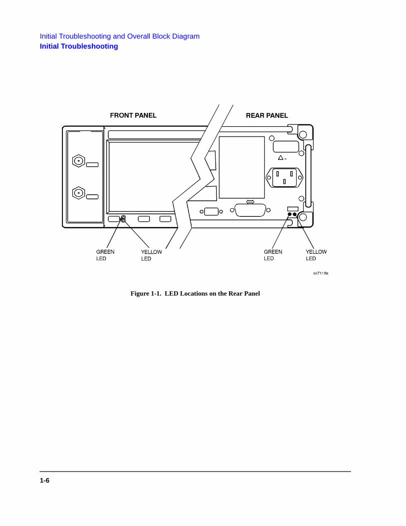
Observing the LEDs on the front and rear panel of the signal generator will determine if there is a catastrophic failure in the power supply assembly.
1. Ensure the signal generator is plugged in (do not switch the power on) and verify that the yellow LED on both the front and rear panels is lit. Refer to Figure 1-1 for LED locations. A lit yellow LED (+15V_STBY) indicates that line voltage is present.
2. Power on the signal generator and verify that the green LED on both the front and rear panels is lit. A lit green LED indicates the power supply has received an “ON” command. The ON/OFF switch toggles a flip-flop latch which biases the proper transistors in the LED control circuit. This circuit is powered by VBAT, the battery-backed SRAM supply, so that the on-off state is “remembered” even when the instrument is unplugged.
1-5
Initial Troubleshooting and Overall Block DiagramInitial Troubleshooting
Figure 1-1. LED Locations on the Rear Panel
1-6

Initial Troubleshooting and Overall Block DiagramInitial Troubleshooting
Step 2: Power On the Signal Generator and Check for Error Messages
This procedure verifies that the signal generator powers up and that the internal instrument check identifies no errors. The internal check evaluates the correctness of operation and returns an error message if a problem is detected.
1. Switch on the signal generator. Let the signal generator warm up for at least five minutes.
NOTE: For signal generators with Option 1E5, ERROR 514, Reference Oven Cold will occur whenever the signal generator is powered up within five minutes of being connected to AC line power. The OVEN COLD annunciator and the ERR annunciator will both turn on. The OVEN COLD annunciator will automatically clear after approximately five minutes. The error queue cannot be cleared, however, until the OVEN COLD annunciator has turned off.
2. Cycle the power to the signal generator and verify that the green LED on both the front and rear panels is lit. Refer to Figure 1-1.
3. When the display is lit, check to see if the ERR annunciator is turned on.
4. If the ERR annunciator is turned on, review the error messages in the queue by pressing Utility, Error Info, View Next Error Message. The first error message in the queue will be shown in the text area of the display. Refer to Chapter 6, "Error Messages," for descriptions of error messages.
If there is more than one error message (each message will be designated as 1 of n), continue pressing the View Next Error Message softkey until you have seen and recorded all of the messages.
5. If you were able to resolve all of the error messages, press Utility, Error Info, Clear Error Queue(s) to delete the list of error messages.
1-7

Initial Troubleshooting and Overall Block DiagramInitial Troubleshooting
Step 3: Functional Check the Front Panel Keys and Display1. Press various front panel hardkeys and softkeys to verify they function as expected.
2. Use the contrast keys to verify that the display can be lightened and darkened. Refer to Figure 1-2.
Figure 1-2. Contrast Keys
1-8

Initial Troubleshooting and Overall Block DiagramInitial Troubleshooting
Step 4: Visually Check the Individual Voltage Supplies1. Unplug the signal generator and remove the instrument cover. Refer to Chapter 4, "Assembly Replacement," for
removal instructions.
2. Expose the motherboard by removing the top cover. It is secured by 11 screws.
3. Plug in the signal generator and allow it to warm up for at least five minutes.
4. If possible, clear the error queue(s) of messages. Press Utility, Error Info, Clear Error Queue(s).
5. On the motherboard, locate the 10 LEDs that correspond to the individual voltage supplies (see Figure 1-3). Verify that all the LEDs are lit. If one or more LEDs are off, proceed to Step 6: Isolate the Failed Assembly.
Figure 1-3. LED Locations on the Motherboard
1-9
Initial Troubleshooting and Overall Block DiagramInitial Troubleshooting
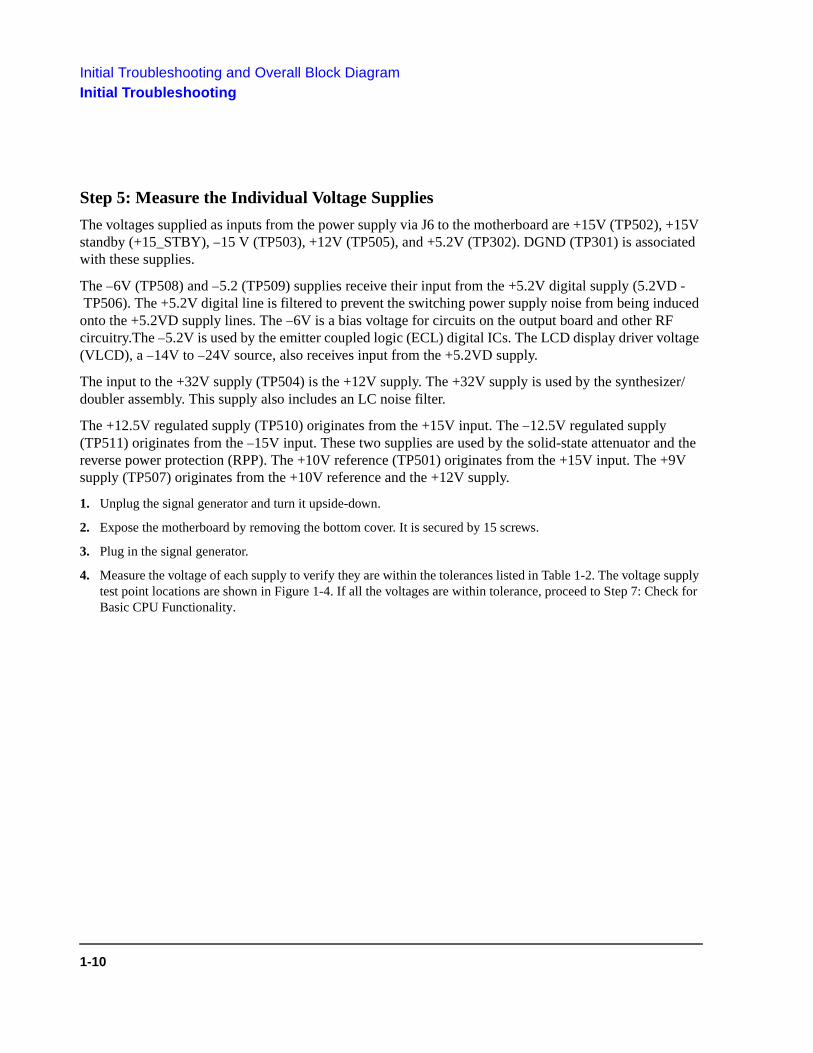
Step 5: Measure the Individual Voltage Supplies
The voltages supplied as inputs from the power supply via J6 to the motherboard are +15V (TP502), +15V standby (+15_STBY), 15 V (TP503), +12V (TP505), and +5.2V (TP302). DGND (TP301) is associated with these supplies.
The 6V (TP508) and 5.2 (TP509) supplies receive their input from the +5.2V digital supply (5.2VD - TP506). The +5.2V digital line is filtered to prevent the switching power supply noise from being induced onto the +5.2VD supply lines. The 6V is a bias voltage for circuits on the output board and other RF circuitry.The 5.2V is used by the emitter coupled logic (ECL) digital ICs. The LCD display driver voltage (VLCD), a 14V to 24V source, also receives input from the +5.2VD supply.
The input to the +32V supply (TP504) is the +12V supply. The +32V supply is used by the synthesizer/doubler assembly. This supply also includes an LC noise filter.
The +12.5V regulated supply (TP510) originates from the +15V input. The 12.5V regulated supply (TP511) originates from the 15V input. These two supplies are used by the solid-state attenuator and the reverse power protection (RPP). The +10V reference (TP501) originates from the +15V input. The +9V supply (TP507) originates from the +10V reference and the +12V supply.
1. Unplug the signal generator and turn it upside-down.
2. Expose the motherboard by removing the bottom cover. It is secured by 15 screws.
3. Plug in the signal generator.
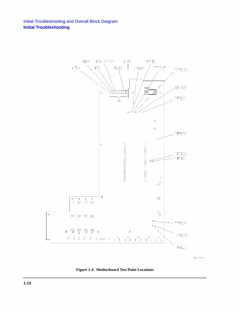
4. Measure the voltage of each supply to verify they are within the tolerances listed in Table 1-2. The voltage supply test point locations are shown in Figure 1-4. If all the voltages are within tolerance, proceed to Step 7: Check for Basic CPU Functionality.
1-10

Initial Troubleshooting and Overall Block DiagramInitial Troubleshooting
Table 1-2. Voltage Supply Tolerances
Test Point Supply Voltage Tolerance
J6 (pins 2, 3, 12, 13) +5.2 +/ 3%
J6 (pin 20) +15 +/ 3%
J6 (pin 18) 15 +/ 3%
J6 (pin 19) +12 +/ 3%
J6 (pin 17) +15 STBY +/ 5%
TP301 DGND N/A
TP302 +5.2V +/ 3%
TP501 +10V_REF +/ 3%
TP502 +15V +/ 3%
TP503 15V +/ 3%
TP504 +32V +/ 4%
TP505 +12V +/ 3%
TP506 +5.2VD +/ 4%
TP507 +9V +/ 4%
TP508 6V +/ 4%
TP509 5.2V +/ 4%
TP510 +12.5V +/ 4%
TP511 12.5V +/ 4%
1-11
Initial Troubleshooting and Overall Block DiagramInitial Troubleshooting
Figure 1-4. Motherboard Test Point Locations
1-12

Initial Troubleshooting and Overall Block DiagramInitial Troubleshooting
Step 6: Isolate the Failed Assembly1. Switch off the signal generator.
2. Remove or disconnect an assembly. Below is a suggested order of removal/disconnection based upon ease.
a A7 Baseband Generator Board (Options 1EH, UN3, UN4)b A8 Data Generator Board (Options UN3, UN4)c A1W1 Front Panel Ribbon Cabled A3W1 Inverter Wire Bundlee W10 Display Ribbon Cablef W13 Attenuator/RPP Ribbon Cableg B1W1 Fan Cable (disconnect only temporarily)h B1W2 Fan Cable (disconnect only temporarily)i A9 Output Boardj A11 Reference Boardk A12 Synthesizer/Doubler Board
NOTE: Refer to Chapter 3, "Replaceable Parts," for information on locating assemblies. Refer to Chapter 4, "Assembly Replacement," for information on removing or disconnecting assemblies.
3. Switch on the signal generator and check the voltage supply LEDs (see Figure 1-3). If the LEDs are lit, you have likely identified the failed assembly. If one or more LEDs are still off, switch off the signal generator and replace/reconnect the assembly and repeat this procedure.
1-13

Initial Troubleshooting and Overall Block DiagramInitial Troubleshooting
Step 7: Check for Basic CPU Functionality
The Digital Signal Processor (DSP) performs a self-diagnostic test at power up. If the DSP is not working, the CPU reports an error.
If the DSP does not seem to be working and the CPU did not report the error, then check the CLK_OUT signal at TP701. It should be a 16 MHz signal. (Refer to Figure 1-5.)
The eight LEDs of DS201 (see Figure 1-5) indicate the status of the boot and flash ROM for the CPU. The LEDs form a binary code that can be described as a tow digit hexadecimal code. Table 1-3 shows the test sequence and the LED pattern (binary representation) of the test that is running. If an error occurs and the test is halted the LED pattern will indicate which self test halted the process. The LED closest to R201 is the place holder for the Least Significant Bit (LSB) in the pattern.
Table 1-3. Sequence for DSP Self-Diagnostic Tests
Test Description Hexadecimal CodeBinary
RepresentationMSB LSB
LEDs at start of test FF 1111 1111
Checksum test FE 1111 1110
Bootrom RAM test FD 1111 1101
RAM test FC 1111 1100
I/O bus test FB 1111 1011
Main firmware checksum test FA 1111 1010
CPU test AA 1010 1010
Test done and OK 00 0000 0000
1-14

Initial Troubleshooting and Overall Block DiagramInitial Troubleshooting
Figure 1-5. Location of TP701 and DS201 on CPU/Motherboard
1-15

Initial Troubleshooting and Overall Block DiagramInitial Troubleshooting
1-16
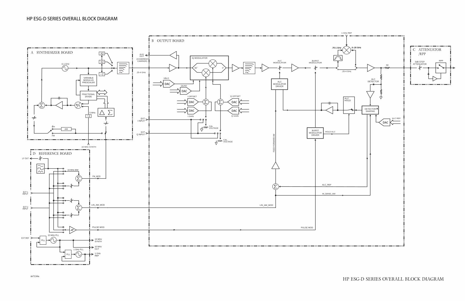
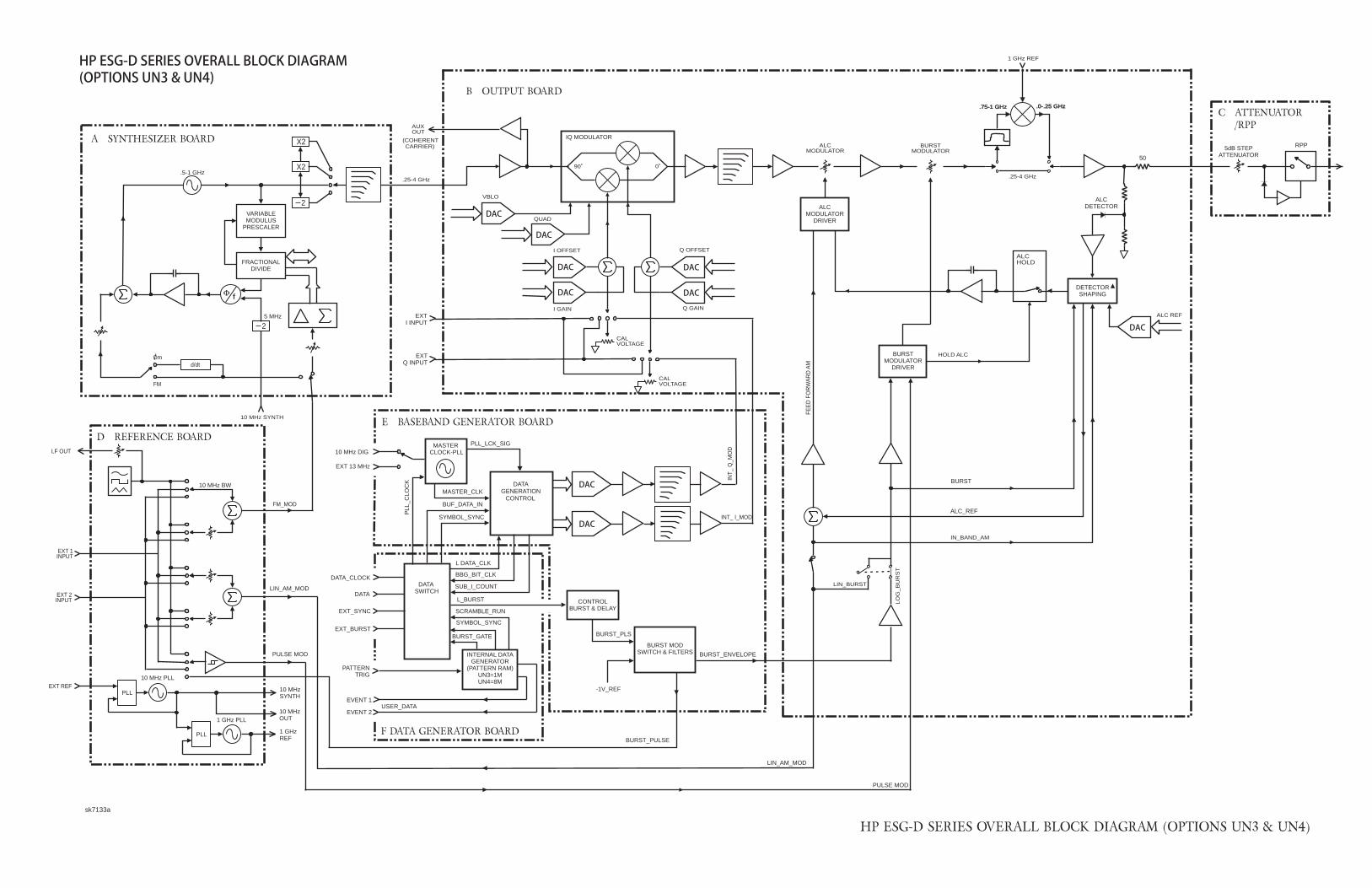
HP ESG-D SERIES OVERALL BLOCK DIAGRAM
LIN_AM_MOD
PULSE MOD
LF OUT
EXT 1INPUT
EXT 2INPUT
EXT REF
B OUTPUT BOARD
1 GHz REF
FE
ED
FO
RW
AR
D A
M
ALCMODULATOR
DRIVER
DETECTORSHAPING
DAC
DAC
DAC
ALCMODULATOR
BURSTMODULATOR
DRIVER
BURSTMODULATOR
.75-1 GHz .0-.25 GHz
.25-4 GHz
0
TAGE
CALVOLTAGE
Q GAIN
Q OFFSET
ALC REF
ALCHOLD
HOLD ALC
IN_BAND_AM
RPP
50
C ATTENUATOR /RPP
5dB STEPATTENUATOR
ALCDETECTOR
ALC_REF
A SYNTHESIZER BOARD
2
2
d/dt
FM
Om/
.5-1 GHz
5 MHz
VARIABLEMODULUS
PRESCALER
FRACTIONALDIVIDE
X2
X2
fΦ
LIN_AM_MOD
D REFERENCE BOARD
FM_MOD
PLL
PLL
10 MHz BW
PULSE MOD
1 GHz PLL
10 MHzSYNTH
1 GHzREF
10 MHzOUT
10 MHz PLL
10 MHz SYNTH
EXTI INPUT
EXTQ INPUT
DAC
DAC
DAC
DAC
IQ MODULATOR
90
VBLO
QUAD
.25-4 GHz
AUXOUT
CARRIER)(COHERENT
CALVOL
I GAIN
I OFFSET
sk7134a
HP ESG-D SERIES OVERALL BLOCK DIAGRAM

Initial Troubleshooting and Overall Block DiagramOverall Block Diagram
1-18

HP ESG-D SERIES OVERALL BLOCK DIAGRAM (OPTION 1EH)
A SYNTHESIZER BOARD X2
LIN_AM_MOD
PULSE MOD
LF OUT
EXT 1INPUT
EXT 2INPUT
EXT REF
FE
ED
FO
RW
AR
D A
M
B OUTPUT BOARD
ALCMODULATOR
DRIVER
DETECTORSHAPING
DAC
DAC
DAC
ALCMODULATOR
BURSTMODULATOR
DRIVER
IQ MODULATOR
BURSTMODULATOR
.75-1 GHz .0-.25 GHz
.25-4 GHz
0
AUXOUT
CARRIER)(COHERENT
TAGE
CALVOLTAGE
Q GAIN
Q OFFSET
ALC REF
ALCHOLD
HOLD ALC
IN_BAND_AM
LIN_BURST
LO
G_
BU
RS
T
1 GHz REF
RPP
50
C ATTENUATOR /RPP
5dB STEPATTENUATOR
ALCDETECTOR
BURST_ENVELOPE
ALC_REF
BURSTINT
_ Q
_M
OD
INT_ I_MOD
BURST MODSWITCH & FILTERS
RST_PULSE
2
2
d/dt
FM
Om/
.5-1 GHz
5 MHz
VARIABLEMODULUS
PRESCALER
FRACTIONALDIVIDE
X2
fΦ
LIN_AM_MOD
D REFERENCE BOARD
FM_MOD
PLL
PLL
10 MHz BW
PULSE MOD
1 GHz PLL
10 MHzSYNTH
1 GHzREF
10 MHzOUT
10 MHz PLL
E BASEBAND GENERATOR BOARD
BURSTGATE
10 MHz DIG
EXT 13 MHz
EVENT 1
PATTERNTRIG
EVENT 2
EXTI INPUT
EXTQ INPUT
DAC
DAC
DAC
DAC
90
VBLO
QUAD
.25-4 GHz
10 MHz SYNTH
CALVOL
I GAIN
I OFFSET
+PTAT
DATASWITCH
MASTERCLOCK-PLL
MASTER_CLK
PLL_LCK_SIG
PL
L_
BU
F_
BIT
_C
LK
EV
EN
T_
SE
LE
CT
INT
_A
LT
_PWR
BIT_CLK_INV
BUF_DATA
L_BURST
INT_BURST
PLL_BUF_BIT_CLK
INT_SYNC
INT_DATA
SYMBOL_SYNC
DATAGENERATION
CONTROL
DAC
DAC
DATA
DATACLK
SYMBCLK
INTERNAL DATA
CONTROLBURST & DELAY
BURST_PLS
BU
GENERATOR
(PATTERN RAM)1Mbit
sk796a HP ESG-D SERIES OVERALL BLOCK DIAGRAM (OPTION 1EH)

Initial Troubleshooting and Overall Block DiagramOverall Block Diagram (Option 1EH)
1-20
HP ESG-D SERIES OVERALL BLOCK DIAGRAM (OPTIONS UN3 & UN4)
A SYNTHESIZER BOARD X2
LIN_AM_MOD
PULSE MOD
LF OUT
EXT 1INPUT
EXT 2INPUT
EXT REF
FE
ED
FO
RW
AR
D A
M
B OUTPUT BOARD
ALCMODULATOR
DRIVER
DETECTORSHAPING
DAC
DAC
DAC
ALCMODULATOR
BURSTMODULATOR
DRIVER
IQ MODULATOR
BURSTMODULATOR
.75-1 GHz .0-.25 GHz
.25-4 GHz
0
AUXOUT
CARRIER)(COHERENT
TAGE
CALVOLTAGE
Q GAIN
Q OFFSET
ALC REF
ALCHOLD
HOLD ALC
IN_BAND_AM
LIN_BURST
LO
G_
BU
RS
T
1 GHz REF
RPP
50
C ATTENUATOR /RPP
5dB STEPATTENUATOR
ALCDETECTOR
BURST_ENVELOPE
ALC_REF
BURSTINT
_ Q
_M
OD
INT_ I_MOD
BURST MODSWITCH & FILTERS
URST_PULSE
2
2
d/dt
FM
Om/
.5-1 GHz
5 MHz
VARIABLEMODULUS
PRESCALER
FRACTIONALDIVIDE
X2
fΦ
LIN_AM_MOD
D REFERENCE BOARD
FM_MOD
PLL
PLL
10 MHz BW
PULSE MOD
1 GHz PLL
10 MHzSYNTH
1 GHzREF
10 MHzOUT
10 MHz PLL
E BASEBAND GENERATOR BOARD
F DATA GENERATOR BOARD
DATA_CLOCK
10 MHz DIG
EXT 13 MHz
EVENT 1
PATTERNTRIG
EVENT 2
EXTI INPUT
EXTQ INPUT
DAC
DAC
DAC
DAC
90
VBLO
QUAD
.25-4 GHz
10 MHz SYNTH
CALVOL
I GAIN
I OFFSET
-1V_REF
DATASWITCH
MASTERCLOCK-PLL
MASTER_CLK
PLL_LCK_SIG
PL
L_
CL
OC
K
L DATA_CLK
BBG_BIT_CLK
SUB_I_COUNT
BUF_DATA_IN
L_BURST
BURST_GATE
USER_DATA
SYMBOL_SYNC
SCRAMBLE_RUN
SYMBOL_SYNC
DATAGENERATION
CONTROL
DAC
DAC
EXT_SYNC
DATA
EXT_BURST
INTERNAL DATAGENERATOR
(PATTERN RAM)UN3=1MUN4=8M
CONTROLBURST & DELAY
BURST_PLS
B
sk7133a
HP ESG-D SERIES OVERALL BLOCK DIAGRAM (OPTIONS UN3 & UN4)

Initial Troubleshooting and Overall Block DiagramOverall Block Diagram (Options UN3 & UN4)
1-22

2 Assembly-Level Troubleshooting with Block Diagrams
This chapter will help you test and troubleshoot the major assemblies of your signal generator. Block diagrams are also provided for each of the assemblies.
2-1

Assembly-Level Troubleshooting with Block DiagramsBefore You Begin Troubleshooting
Before You Begin Troubleshooting
Avoid Personal Injury
WARNING: These servicing instructions are for use by qualified personal only. To avoid electrical shock, do not perform any servicing unless you are qualified to do so.
WARNING: The opening of covers or removal of parts is likely to expose dangerous voltages. Disconnect the product from all voltage sources while it is being opened.
WARNING: The detachable power cord is the instrument disconnecting device. It disconnects the mains circuits from the mains supply before other parts of the instrument. The front panel switch is only a standby switch and is not a LINE switch.
WARNING: The power cord is connected to internal capacitors that may remain live for 5 seconds after disconnecting the plug from its power supply.
Prevent ESD Damage
CAUTION: Many of the assemblies in this instrument are very susceptible to damage from ESD (electrostatic discharge). Perform service procedures only at a static-safe workstation and wear a grounding strap.
2-2

Assembly-Level Troubleshooting with Block DiagramsUsing the Procedures in this Chapter
Using the Procedures in this Chapter
This chapter contains a troubleshooting procedure for each of the following assemblies in your signal generator:
• A9 Output Board
• A11 Reference Board
• A12 Synthesizer Board
• A14 CPU/Motherboard
Each procedure consists of the following:
• A table listing the tests in the order they should be performed. The table also provides test conditions and expected node voltages for each test.
• A block diagram of the assembly.
You Will Need Software
To perform the tests in this chapter you must use the service software that came with your signal generator. The service software has a utility program that measures and displays the node voltages for each test. Refer to your signal generator’s calibration guide for information on using the software.
Additional Block Diagrams
The following block diagrams can be found at the end of this chapter:
• AT1 Attenuator/RPP
• A7 Baseband Generator Board - Option 1EH
• A7 Baseband Generator Board - Options UN3 & UN4
• A8 Data Generator Board - Options UN3 & UN4
• Power Supply and Ground Interconnects
• Modulation & Signal Interconnects
2-3

Assembly-Level Troubleshooting with Block DiagramsUsing the Procedures in this Chapter
2-4
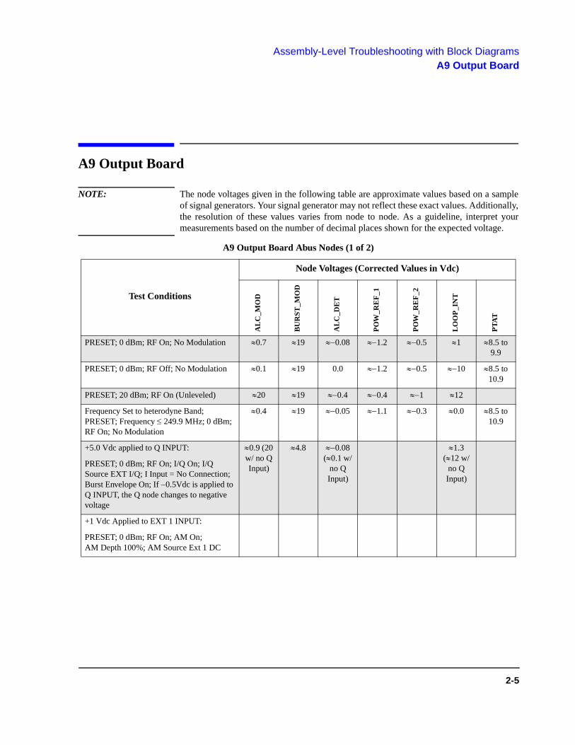
Assembly-Level Troubleshooting with Block DiagramsA9 Output Board
A9 Output Board
NOTE: The node voltages given in the following table are approximate values based on a sample of signal generators. Your signal generator may not reflect these exact values. Additionally, the resolution of these values varies from node to node. As a guideline, interpret your measurements based on the number of decimal places shown for the expected voltage.
A9 Output Board Abus Nodes (1 of 2)
Test Conditions
Node Voltages (Corrected Values in Vdc)A
LC
_MO
D
BU
RST
_MO
D
AL
C_D
ET
PO
W_R
EF
_1
PO
W_R
EF
_2
LO
OP
_IN
T
PTA
T
PRESET; 0 dBm; RF On; No Modulation 0.7 19 0.08 1.2 0.5 1 8.5 to 9.9
PRESET; 0 dBm; RF Off; No Modulation 0.1 19 0.0 1.2 0.5 10 8.5 to 10.9
PRESET; 20 dBm; RF On (Unleveled) 20 19 0.4 0.4 1 12
Frequency Set to heterodyne Band; PRESET; Frequency 249.9 MHz; 0 dBm; RF On; No Modulation
0.4 19 0.05 1.1 0.3 0.0 8.5 to 10.9
+5.0 Vdc applied to Q INPUT:
PRESET; 0 dBm; RF On; I/Q On; I/Q Source EXT I/Q; I Input = No Connection; Burst Envelope On; If 0.5Vdc is applied to Q INPUT, the Q node changes to negative voltage
0.9 (20 w/ no Q Input)
4.8 0.08 (0.1 w/
no Q Input)
1.3 (12 w/
no Q Input)
+1 Vdc Applied to EXT 1 INPUT:
PRESET; 0 dBm; RF On; AM On; AM Depth 100%; AM Source Ext 1 DC
2-5

Assembly-Level Troubleshooting with Block DiagramsA9 Output Board
A9 Output Board Abus Nodes (2 of 2)
Test Conditions
Node Voltages (Corrected Values in Vdc)
I Q PR
E_L
EV
EL
QU
AD
GA
IN_D
ET
GR
D
RE
F_A
M
PRESET; 0 dBm; RF On; No Modulation 0.8 0 2 2 0.2 0.00 0.3
PRESET; 0 dBm; RF Off; No Modulation 0.8 0 2 2 0.2 0.00 0.3
PRESET; 20 dBm; RF On (Unleveled)
Frequency Set to heterodyne Band; PRESET; Frequency 249.9 MHz; 0 dBm; RF On; No Modulation
0.5 0 2 3 0.2 0.00 0.2
+5.0 Vdc applied to Q INPUT:
PRESET; 0 dBm; RF On; I/Q On; I/Q Source EXT I/Q; I Input = No Connection; Burst Envelope On; If 0.5Vdc is applied to Q INPUT, the Q node changes to negative voltage
0 0.8 0.2 (0.0 w/ no Q Input)
+1 Vdc Applied to EXT 1 INPUT:
PRESET; 0 dBm; RF On; AM On; AM Depth 100%; AM Source Ext 1 DC
1
2-6

A9 OUTPUT BLOCK DIAGRAM
ABUS
ALC MOD BURST MOD
ALC MOD
DRIVEBURST MOD
DRIVE
MIXER700 - 1000 MHz
BPF
300 MHz
LPF
1 GHz REFERENCE
P1-19
FROM: REFERENCEASSY P1-19
J6
I MOD DRIVE
P1-2
EN LIN AM
LIN_AM_ MOD
ABUS
ABUS
I OFFSET
DET OFFSET
Q OFFSET
DAC
DAC
DAC
DAC
DAC
I GAIN
Q GAIN
I MOD DRIVE
ALC DETECTOR INPUT
ALC REFERENCE REFERENCE+ AM
ALC MOD DRIVE
AM IMPUT
Q MOD DRIVE
I MOD SELECT
FROM: REFERENCEASSY P6
Q MOD SELECT
P3-6
INT_I_MOD
EXT_I_MOD
EXT_Q_MOD
INT_Q_MOD
EXT_Q_MOD
EXT_I_MOD
CAL
VOLTAGES
CAL
VOLTAGES
REF
REF
I
STEP
ATTENUATOR
LOG
AMP
AMP
LOG
BURST
MOD
DRIVER
Q
STEP
ATTENUATOR
Q MOD DRIVE
ABUS
I MOD DRIVE
ABUS
ABUSABUS
HZ LPF
HZ LPF
HZ LPF
HZ LPF
HZ LPF
DAC
DAC
DAC
DAC
DAC
DAC
DAC
GAIN DETECTOR
F >250 MHz
F < 250 MHz F <250 MHz
F >250 MHz
250 MHz TO 4000 MHz
0 dBm + -5dB DET BW
SEL
DET
VOLTAGE
RF OUT
.250 TO 4000 MHz
MAX POWER >17 dBm
P3-15
DET
VOLTAGE
ALT ALC REF
ALC REF
&
&
BURST MOD DRIVE ALC HOLD
BURST MOD OFFSET
BURST MOD BIAS
OPEN =
HOLD MAIN INT
CLOSED =
RF OFF ALT INT
CLOSED =
RF OFF MAIN INT
OPEN =
HOLD ALT INT
-6V
CLOSED =
RF OFF
(BURST MOD)
L RF OFF (BURST MOD)PULSE MOD
P2-23FROM: REFERENCE ASSYP3-7
FROM: BASEBAND GENERATOR ASSYP301-31
+V
+V
ABUS
LOOP INT
ALC MOD BIAS
ABUS
ALC MOD
ALC UNLEVELEDDETECTOR
+
+
_
_
-15V
OPEN
OPEN LOOP
CLOSED =
RF OFF (ALC MOD)
ALC MOD
DRIVER
ALT POWERSELECT LOGIC
BW SELECT
ALT POWER SELECT
BW SELECT
FROM: BASEBAND GENERATOR ASSY P301-80
L ALT PWR SEL
P2-10
FEED FORWARD AM
ALT POWER SELECT
L UNLEVELED
ALC
MOD
DRIVE
ALC REF SELECT
L ALC HOLD
L HOLD ALC
DEEP AM MOD
L RF OFF ALC MOD
HOLD MAIN
INT
HOLD ALT
INT
BULK R
ADJUSTMENT
LOG DET
ALC DET
ALC REF
SELECT
OPEN=
OPEN LOOP
IN BAND AM
PWR REF
REF + AM
REF AM
LOG OFFSET
FEED FORWARD AM
BURST
MOD
DRIVE
BURST MOD
BURST ENBURST GAIN
REF
EN LIN BURST
EN LOG BURST
FADE ENVELOPE
(NOT USED)
BURST ENVELOPE
P1-17
P1-6
FROM: BASEBANDGENERATOR ASSYP301-57
FROM: REFERENCEASSYP3-17
P2-22
RF PATH
TO: STEP ATTENUATORASSY J2
DACDAC
DAC
DAC
ABUS
ABUS
I/Q
MODULATOR
+
VBLO QUAD Q I
I DET Q DET
AUX OUT
TO: COHERENT CARRIER
RF IN
250 to 4000 MHz
>+10 dBm
FROM: SYNTHEIZER
ASSY J6
J4
PRELEVEL DET
PRELEVEL
PRELEVEL REF
PRELEVEL MOD DRIVE
P3-4
TO: SYNTHESIZER ASSYP3-17
GAIN ADJUST
Q MOD DRIVEQUAD DAC
QUAD
VBLO DAC
ENABLE/INTERRUPT
P2-25
DIGITALINTERFACE
SELECT
DATA
CLK
CLK
DATA
ENABLE/INTRPT
INT 1
INT2
INT3
INT4 (Serial Data)
SERIAL I/O
DIGITAL
CONTROL
EEPROM
CLK P2-24
DATA P2-11
+5V
+5V
L UNLEVELED
+5V
ABUS
ABUS
POWER SUPPLIES INPUTS
P2-6,21
P2-5,20
P2-14,29
P2-3,18
P2-1,17
+15V
+9V
+5.2V
-6V
-15V
TEMPERATURE
COMPENSATION
POWER SUPPLY
PTAT
GND
+PTAT
P1-15
8.5 TO 9.9V
2400 M
1550 M
1000 M
628 M
396 M
P3-19
J5
EXT Q MOD
EXT I MOD
P3-8
FROM: Q INPUT
FROM: I INPUT
P2-1,16
P2-15,30
ANALOG COMMON
DIGITAL COMMON
DEEP AM LEVEL DETECTORREF + AM
A9 OUTPUT BLOCK DIAGRAMsk797a

Assembly-Level Troubleshooting with Block DiagramsA9 Output Board Block Diagram
2-8

Assembly-Level Troubleshooting with Block DiagramsA11 Reference Board
A11 Reference Board
NOTE: The node voltages given in the following table are approximate values based on a sample of signal generators. Your signal generator may not reflect these exact values. Additionally, the resolution of these values varies from node to node. As a guideline, interpret your measurements based on the number of decimal places shown for the expected voltage.
A11 Reference Board Abus Nodes
Test Conditions
Node Voltages (Corrected Values in Vdc)
MO
D1_
OU
T
MO
D2_
OU
T
VT
UN
E
MO
D1_
PK
MO
D2_
PK
LIN
_AM
1GH
Z_D
ET
FM
_MO
D
PRESET; No Modulation 0.00 0.00 2 to 4 < 0.5 < 0.5 0.00 0.0 < 0.3
Frequency Set to Heterodyne Band:
PRESET; Frequency 249.9 MHz; No Modulation
2 to 4 > 0.15
+1 Vdc Applied to EXT 1 INPUT:
PRESET; FM On; FM Source Ext 1 DC
1.9 0.00 2 to 4 < 0.5 < 0.5 0.0 2.2
+1 Vdc Applied to EXT 2 INPUT:
PRESET; FM On; FM Source Ext 2 DC
0 0.00 2 to 4 7.5 < 0.5 0.0 0
1 Vpp @ 1 kHz Applied to EXT 1 INPUT:
PRESET; FM On; FM Source Ext 1 AC
1.9 0.00 2 to 4 < 0.5 < 0.5 2.0 0.0
1 Vpp @ 1 kHz Applied to EXT 2 INPUT:
PRESET; FM On; FM Source Ext 2 AC
0 0.00 2 to 4 7.5 < 0.5 0 0.0
+1 Vdc Applied to EXT 1 INPUT:
PRESET; AM On; AM Depth 100%; AM Source Ext 1 DC
0.00 1.9 2 to 4 < 0.5 < 0.5 0.0 2.2
+1 Vdc Applied to EXT 2 INPUT:
PRESET; AM On; AM Depth 100%; AM Source Ext 2 DC
0.00 0 2 to 4 < 0.5 7.5 0.0 0
2-9

Assembly-Level Troubleshooting with Block DiagramsA11 Reference Board
1 Vpp @ 1 kHz Applied to EXT 1 INPUT:
PRESET; AM On; AM Depth 100%; AM Source Ext 1 AC
0.00 1.9 2 to 4 < 0.5 < 0.5 2.0 0.0
1 Vpp @ 1 kHz Applied to EXT 2 INPUT:
PRESET; AM On; AM Depth 100%; AM Source Ext 2 AC
0.00 0 2 to 4 < 0.5 7.5 0 0.0
A11 Reference Board Abus Nodes
Test Conditions
Node Voltages (Corrected Values in Vdc)
MO
D1_
OU
T
MO
D2_
OU
T
VT
UN
E
MO
D1_
PK
MO
D2_
PK
LIN
_AM
1GH
Z_D
ET
FM
_MO
D
2-10
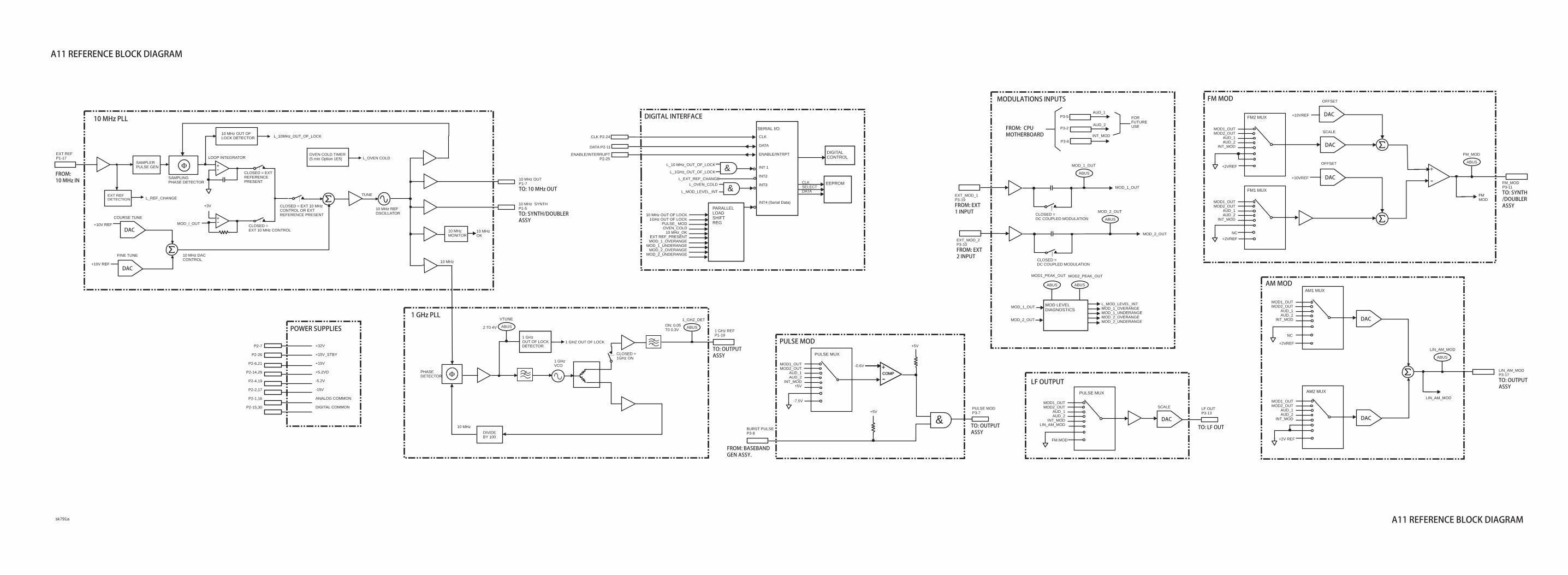
A11 REFERENCE BLOCK DIAGRAM
10 MHz
10 MHzMONITOR
1 GHz PLL
ΦPHASEDETECTOR
DIVIDEBY 100
1 GHzOUT OF LOCKDETECTOR
CLOSED =1GHz ON
1 GHzVCO
ABUS
VTUNE
2 T0 4V ABUS
1_GHZ_DET
ON: 0.05 T0 0.3V 1 GHz REF
P1-19
1 GHZ OUT OF LOCK
10 MHz
DIGITAL INTERFACE
CLKSELECTDATA
CLK
DATA
ENABLE/INTRPT
INT 1
INT2
INT3
INT4 (Serial Data)
SERIAL I/O
DIGITALCONTROL
EEPROM
PARALLELLOADSHIFTREG
10 MHz OUT OF LOCK1GHz OUT OF LOCK
PULSE_ MODOVEN_COLD
10 MHz_OKEXT REF_PRESENTMOD_1_OVERANGE
MOD_1_UNDERANGEMOD_2_OVERANGE
MOD_2_UNDERANGE
&L_OVEN_COLD
L_MOD_LEVEL_INT
&L_10 MHz_OUT_OF_LOCK
L_1GHz_OUT_OF_LOCK
CLK P2-24
DATA P2-11
ENABLE/INTERRUPTP2-25
10 MHz OUTP1-7
TO: 10 MHz OUT
10 MHz SYNTHP1-5
TO: SYNTH/DOUBLERASSY
10 MHzOK
MODULATIONS INPUTS
ABUS
ABUS
MOD_1_OUT
MOD_2_OUT
FOR FUTURE USE
AUD_1
AUD_2
INT_MOD
P3-5
P3-2
P3-6
FROM: CPUMOTHERBOARD
MOD_1_OUT
MOD_2_OUT
CLOSED =DC COUPLED MODULATION
CLOSED =DC COUPLED MODULATION
MOD LEVELDIAGNOSTICS
ABUSABUS
MOD1_PEAK_OUT MOD2_PEAK_OUT
MOD_1_OUT
MOD_2_OUT
L_MOD_LEVEL_INTMOD_1_OVERANGEMOD_1_UNDERANGEMOD_2_OVERANGEMOD_2_UNDERANGE
EXT_MOD_1P3-19
FROM: EXT 1 INPUT
EXT_MOD_2P3-10
FROM: EXT 2 INPUT
+
PULSE MOD
PULSE MUX
&
MOD1_OUTMOD2_OUT
AUD_1AUD_2
INT_MOD+5V
-7.5V
COMP
+COMP
+-0.6V
PULSE MODP3-7
TO: OUTPUTASSY
+5V
+5V
LF OUTPUT
DAC
PULSE MUX
MOD1_OUTMOD2_OUT
AUD_1AUD_2
INT_MODLIN_AM_MOD
FM.MOD
LF OUTP3-13
TO: LF OUT
SCALE
FM MOD
ABUS
FM_MOD
DAC
DAC
DACFM2 MUX
FM1 MUX
MOD1_OUTMOD2_OUT
AUD_1AUD_2
INT_MOD
MOD1_OUTMOD2_OUT
AUD_1AUD_2
INT_MOD
+2VREF
+2VREF
NC
AM MOD
ABUS
LIN_AM_MOD
DAC
AM1 MUX
MOD1_OUTMOD2_OUT
AUD_1AUD_2
INT_MOD
+2VREF
NC
DAC
AM2 MUX
MOD1_OUTMOD2_OUT
AUD_1AUD_2
INT_MOD
+2V REF
LIN_AM_MODP3-17
TO: OUTPUT ASSY
FM_MODP3-11
TO: SYNTH/DOUBLER ASSY
+10VREF
+10VREF
OFFSET
SCALE
OFFSET
TO: OUTPUTASSY
L_EXT_REF_CHANGE
FMMOD
LIN_AM_MOD
BURST PULSEP3-8
FROM: BASEBANDGEN ASSY.
10 MHz PLL
EXT REFP1-17
FROM:10 MHz IN
SAMPLERPULSE GEN
SAMPLINGPHASE DETECTOR
10 MHz OUT OFLOCK DETECTOR
EXT REFDETECTION L_REF_CHANGE
10 MHz DACCONTROL
COURSE TUNE
+10V REF
+10V REF
DAC
DAC
FINE TUNE
Φ +-
+-
CLOSED =EXT 10 MHz CONTROL
+3V
MOD_I_OUT
CLOSED = EXT 10 MHzCONTROL OR EXT REFERENCE PRESENT
CLOSED = EXT REFERENCEPRESENT
L_10MHz_OUT_OF_LOCK
LOOP INTEGRATOR
TUNE
OVEN COLD TIMER(5 min Option 1E5) L_OVEN COLD
10 MHz REFOSCILLATOR
POWER SUPPLIES
P2-7
P2-26
P2-6,21
P2-14,29
P2-4,19
P2-2,17
P2-1,16
P2-15,30
+32V
+15V_STBY
+15V
+5.2VD
-5.2V
-15V
ANALOG COMMON
DIGITAL COMMON
A11 REFERENCE BLOCK DIAGRAMsk791a

Assembly-Level Troubleshooting with Block DiagramsA11 Reference Board Block Diagram
2-12
Assembly-Level Troubleshooting with Block DiagramsA12 Synthesizer/Doubler Board
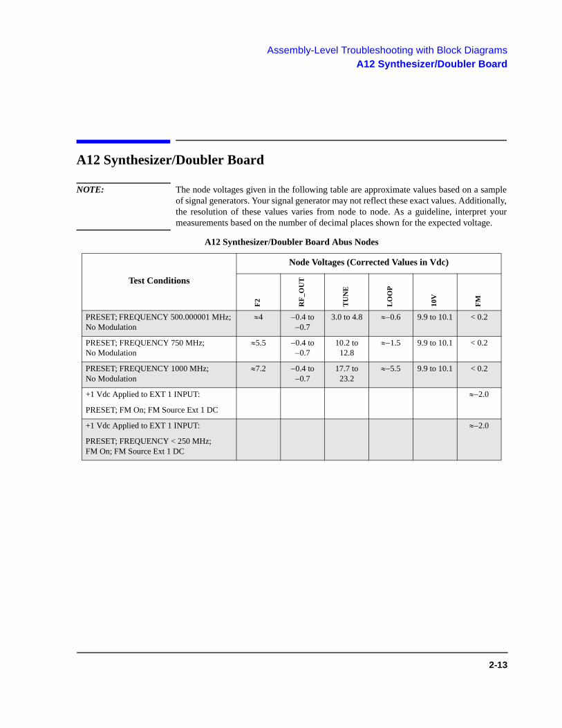
A12 Synthesizer/Doubler Board
NOTE: The node voltages given in the following table are approximate values based on a sample of signal generators. Your signal generator may not reflect these exact values. Additionally, the resolution of these values varies from node to node. As a guideline, interpret your measurements based on the number of decimal places shown for the expected voltage.
A12 Synthesizer/Doubler Board Abus Nodes
Test Conditions
Node Voltages (Corrected Values in Vdc)F
2
RF
_OU
T
TU
NE
LO
OP
10V
FM
PRESET; FREQUENCY 500.000001 MHz; No Modulation
4 0.4 to0.7
3.0 to 4.8 0.6 9.9 to 10.1 < 0.2
PRESET; FREQUENCY 750 MHz; No Modulation
5.5 0.4 to0.7
10.2 to 12.8
1.5 9.9 to 10.1 < 0.2
PRESET; FREQUENCY 1000 MHz; No Modulation
7.2 0.4 to0.7
17.7 to 23.2
5.5 9.9 to 10.1 < 0.2
+1 Vdc Applied to EXT 1 INPUT:
PRESET; FM On; FM Source Ext 1 DC
2.0
+1 Vdc Applied to EXT 1 INPUT:
PRESET; FREQUENCY < 250 MHz; FM On; FM Source Ext 1 DC
2.0
2-13

Assembly-Level Troubleshooting with Block DiagramsA12 Synthesizer/Doubler Board
2-14

A12 SYNTH/DOUBLER BLOCK DIAGRAM
ABUSLOOP GAIN
SYNTHESIZEROUT OF LOCK
DETECTORLOOP
0.02 to -10.1 V
1
FROM
IDE-BY-2
2
250-500 MHz
500-1000 MHz
BANDPASS FILTERS
628-1000 MHz
396-628 MHz
250-396 MHz
X2
1ST DOUBLER
1.6-2.0 GHz
1.26-1.6 GHz
1-1.26 GHz
X2
2ND DOUBLER
3.2-4.0 GHz
2.52-3.2 GHz
2.0-2.52 GHz
FROM OUTPUT ASSYP3-4
P3-17
>2 GHz TO 4 GHz
250 MHz TO 1000 MHz
>1 GHz TO 2 GHz
PRE-LEVEL MOD DRIVE
PRE-LEVELMOD
ABUS
RF OUT
RF OUT
250 MHz TO 4GHz> +10 dBm
J6_
TO OUTPUT ASSYJ4
-0.45 TO -0.7V
OUTPUT
ABUS
POWER SUPPLY INPUTS
REG
+10V
P2-5,20
P2-14,29
P2-4,19
P2-3,18
P2-2,17
P2-1,16
+15V
+10V
9.9 T O 10.1V
+32V
+10V
+9V
+5.2V
-5.2V
-6V
-15V
ANALOG COMMON
P2-7
P2-6,21
FRO
FRO
s
Φ
ABUS
ABUSVCO TUNE
3 T0 32.2V
500-1000 MHz
DAC
Loop Filter&
Lead/Lag
VCO
Frac-NDivide
+10 V
25 MHz
VCO FM
(NOT USED)
0 MHz SYNTH
P3-15 REFERENCE ASSY
P1-6
LOCK ANGLEADJUSTMENT
F/2VCOBIAS
LOOP BWCONTROL
DIV
ABUS
FM
3
DAC
DAC
FMDELAY
A/DCONVERTER
FMATTENUATORS
FM INPUT
FM IN-BAND
FM OUT-OF-BAND
DIGITAL INTERFACE
FROM MOTHERBOARD/CPU ASSYJ5-23
FROM MOTHERBOARD/CPU ASSYJ5-20
FROM MOTHERBOARD/CPU ASSYJ5-26
SERIAL I/O
INT 1
INT 2
INT 3
INT 4(SERIAL DATA)
CLK
DATA
ENABLE/INTERRUPT
CLK
DATA
ENABLE/INTERRUPT
L_OUT OF LOCK
NOT USED
NOT USED
SER_DATA_OUT
(FRAC-N DIVIDER)
CLK
SELECT
DATAEEPROM
P2-24
P2-25
P2-11
DIGITAL
CONTROL
MOD_STRB
P1-20M MOTHERBOARD/
CPU ASSYJ5-54
FM INPUT
P1-1M REFERENCE ASSY
P3-11
A12 SYNTH/DOUBLER BLOCK DIAGRAMP2-15,30 DIGITAL COMMON
k792a

Assembly-Level Troubleshooting with Block DiagramsA12 Synthesizer/Doubler Board Block Diagram
2-16

Assembly-Level Troubleshooting with Block DiagramsA14 CPU/Motherboard
A14 CPU/Motherboard
NOTE: The node voltages given in the following table are approximate values based on a sample of signal generators. Your signal generator may not reflect these exact values. Additionally, the resolution of these values varies from node to node. As a guideline, interpret your measurements based on the number of decimal places shown for the expected voltage.
A14 CPU/Motherboard Abus Nodes
Test Conditions
Node Voltages (Corrected Values in Vdc)
DIS
P
LC
D
INT
_MO
D
P10
V_R
EF
M6V
M5V
P9V
AC
OM
PRESET; 5.3 0.00 10 6.0 5.2 9.0 0.00
PRESET; Vary Display Brightness 1 to 50 0.4 to 1.3
2-17

Assembly-Level Troubleshooting with Block DiagramsA14 CPU/Motherboard
2-18

A14 CPU/MOTHERBOARD BLOCK DIAGRAM (1 OF 2)
CPU CLOCK
CPU INTERFACE
MEMORY
CPU
SERIAL INTERFACE(INTERNAL)
ATTENUATOR& RPP INTERFACE
DIGITAL SIGNAL PROCESSOR (DSP)
32.77 kHz
INTERNALDATA BUS
SERIAL I/OBUS
SERIAL I/O
INTERFACE
TO: DAUGHTERBOARD
J5-24
J5-21
J5-18
J5-26
J5-23
J5-20
J5-76
J5-73
J5-70
J14-17
J14-11
J14-10
J14-9
J14-7
J14-6
J14-5
J14-4
J14-3
J14-2
J14-20
J14-19
J14-18
J14-12
J14-16
J14-1
J14-14
J14-15
J14-13
J14-8
HP-IBINTERFACE
INTERNALDATA BUS
INT ADDRBUS
HP-IB
INTERFACE
LATN
L EOI
L SRQ
L REN
L IFC
L DAV
NDAC
NRFD
DIO1
DIO2
DIO3
DIO4
DIO5
DIO6
DIO7
DIO8
TO: HP-IB
J7-11
J7-5
J7-10
J7-17
J7-9
J7-6
J7-8
J7-7
J7-1
J7-2
J7-3
J7-4
J7-13
J7-14
J7-15
J7-16
L HP-IB INT
L SERIALI/O INT
DACDAC
DACDAC
ABUS
INT MOD
SS
S
T
INT CONTBUS
MEM ADDRBUS
MEM DATABUS
INT ADDRBUS
INTERNAL DATABUS
FLASHMEMORY1M X 16
EEROM64K X 8
NONVOLATILERAM128K X 16
RAM128K X 16
MEM ADDRBUS
MEM ADDRBUS
MEM ADDRBUS
MEM ADDRBUS
MEM DATABUS
MEM DATABUS
MEM DATABUS
MEM DATABUS
REF ENABLE
REF CLK
REF DATA
SYNTH ENABLE
SYNTH CLK
SYNTH DATA
OUTPUT ENABLE
OUTPUT CLK
OUTPUT DATA
L = LF ATTEN
L = HF ATTEN
ATTEN 40B
ATTEN 5A
ATTEN 10A
ATTEN 10B
ATTEN 40A
ATTEN 5B
ATTEN 20
ATTEN XX
ATTEN ENABLE
ATTEN CLK
ATTEN DATA
L RPP INT
L RPP RESET
ATTEN ENABLE
ATTEN CLK
ATTEN DATA
L DCC ALTPWR SEL
TRIG INT
INTERNAL DATA BUS
HFATTENCONTROL
ATTENSENSE
+15V
+12.5V
+5.2V
-12.5V
ACOM
L RPP INT
L RPP RESET
INTERNAL MODULATIONDAC
TRIGGER I/O
10 MHz IN/OUT
CPU TRIG OUTDCC TRIG OUTDSP TRIG OUT
CPU TRIG INTDCC TRIG INTTRIG INT
TRIGENABLE
TRIGENABLE
TRIGGER
IN
TRIGGERIN
10 MHzOUT
10 MHzIN
J11
TRIGGEROUT
J10
J12
J13
FROM:DAUGHTERBOARD
TO:DAUGHTERBOARD
DSP TRIG OUT
L DSP INT
CLK OUT
TP701
RESET
ANALOG TO DIGITALCONVERTER (ADC)
TRIG INT
SWEEP RAMP
INT ADDR BUS
DSP ADDR BUS
DSP DATA BUSINTERNAL DATA BUS
16 MHzCLOCK
DSP/CPUINTERFACE
DIGITALSIGNALPROCESSOR
SERIAL INTERFACE SERIAL INTERFACE
DSP ADDR BUS
DSP RAM
DSP DATA BUS
DSPRAM32K X 8
+
+
SWEEPOUT
J9
TP705TP706
TO: DAUGHTERBOARD
+10V REF
SWEEP RAMP
A BUS
BUF ABUSBUF ABUS
ABUS
ABUS RTN
TP703
TP702
ADC INTP704
+5V
ADC
SERIAL INTERFACE(EXTERNAL)
CLOCK
RS-232SERIALINTERFACE
+5V
J8-2
J8-8
J8-3J8-7
J8-4
J8-5
RECV
CTS
XMIT
RTS
+5V
IRQ 1IRQ2IRQ3IRQ4IRQ5IRQ6IRQ7
TP CLKTPU 0TPU1TPU2TPU3TPU4TPU5TPU6TPU7TPU8
TPU10
L SERIAL I/O INTNOT USEDL HP-IB INTL RPG INT
NOT USEDL KEY INT
NOT USED
10 MHz DIGCOUNTER
CPU TRIG INTL DSP INT
DIG BUS INT 1DIG BUS INT 2DIG BUS INT 3DIG BUS INT 4
PULSE INTL RPP INT
CTS
RXD
TXD
L PRESET
L HALT
FLASH PROGRAMVOLTAGE
SWITCH &LEDS
INTERNALDATA BUS
INTERNALDATA BUS
ENABLEFLASHPROGRAM
VOLTAGEREG+15V FLASH
VPP
TP303
PROGRAM = +12V
SELF TESTLEDS
CONFIGSWITCH
INT ADDRBUS
FROM: AUXILIARYINTERFACE
ADDRESBUFFER
DATABUFFER
BUSCONTROL
BOOROM
ADDRESS BUS
CPU DATA BUS
SERIAL I/O BUS
CPU DATA BUS
A14 CPU/MOTHERBOARD BLOCK DIAGRAM (1 0F 2)sk7113a

Assembly-Level Troubleshooting with Block DiagramsA14 CPU/Motherboard Block Diagram (1 of 2)
2-20

A14 CPU/MOTHERBOARD BLOCK DIAGRAM (2 OF 2)
LCD CONTROLLER
DISPLAY
ENABLE J21-4
+5V J21-5
SHIFT14.32 MHz
TO FRONT PANEL
KEYROW 0
KEYROW 1
KEYROW 2
KEYROW 3
KEYROW 4
RNAL DATA BUS
KEYROW 5
KEYROW 6
KEYROW 7
J20-17
J20-19
J20-21
J20-23
J20-25
J20-26
J20-24
J2-22
KEYBOARD DECODER
ANEL
KEYCOL 0
KEYCOL 1
KEYCOL 2
KEYCOL 3
KEYCOL 4
KEYCOL 5
KEYCOL 6
KEYCOL 7
J20-1
J20-3
L KEY INT
KEYBOARD
COLUMN
DECODER
INTERNAL DATA BUS
RPG
DECODER
RPG A
RPG B
L RPG INT
TO RPG
INTERNAL DATA BUS
J20-12+5V
R
KEYBOARD
ROW
LATCH
L PWRONJ6-1TO PWR SUPPLY
TO FRONT
PANEL
POWER
SWITCH
LATCH
N/OFF SW
L
PWR GREENJ20-2
J20-4STBY YELLOW
+15V STBY }
TP502
TP502
TP506
TP502
SUPPLY
FILTERING
+15V STANDBY
+15V
-15V
+12V
+5.2V+5.2VD
+5.2V
J6-17
J6-20
J6-18
J6-19
J6-2,3,
12,13
+15V STBY
+15V
DS502
DS502
-15V
+12V
FROM POWER SUPPLY
POWER SUPPLY INPUTSPOWER SUPPLY REGULATORS
DIGITAL CARD CAGE CONNECTIONS DAUGHTER BOARD CONNECTIONSTP510
+12.5V
REG+15V +12.5V
DS504
TP501
+10V
REG+15V +10VREF
P10V_REF
TP507
+9V
REG+10VREF +9V
P9V
DS504
ABUS
ABUS
TP511
-12.5V
REG-15V +12.5V
DS505
SWITCHING POWER SUPPLIES
ABUS
ABUS
NEGATIVE
SWITCHING
SUPPLIES
+5.2VD -5.2V
M5V
M6V
DS503-H
TP509
TP508
-6V
DS503-G
TP504
SWITCHING
SUPPLY+12V +32V
POWER SUPPLY DIAGNOSTICS
POWER
SUPPLY
DIAGNOSTICS
+32V
+15V
+12V
-15V
+5.2VD
DS503-A
LOW=+32V OK
LOW=+15V OK
LOW=+12V OK
LOW=-15V OK
+5.2VD
DS503-E DS503-B DS503-DDS503-C
J29-1
SENSE
LOW RESET
POWER RESET
POWER
RESET
+5.2VD
+5.2VDL PRESET
L HALT
L STANDBY
NONVOLATILE MEMORY POWER
V BAT
SELECT
+5.2VD
+5.1V
+3V
BT1
+15V STANDBY
VBAT
FAN POWER SUPPLY
+12V
+12V FAN+
FAN+
J16-1
J16-2
J17-1
J17-2
SERIAL I/O SIGNALS
POWER SUPPLIES
MNEMONIC J5
18
21
24
20
23
26
70
73
76
REF DATA
REF CLK
REF ENABLE
SYNTH DATA
SYNTH CLK
SYNTH ENABLE
OUTPUT DATA
OUTPUT CLK
OUTPUT ENABLE
MNEMONIC J5
83
32,82
33
34,84
30,31
80,81
35,85
37,87
36,86
4,10
16,22
28,51
57,63
69,75
43,47
49,96
+32V
+15V
+15V STBY
+9V
+5.2V
-5.2V
-6V
-15V
DCOM
ACOM
MNEMONIC J5
40
97
99
98,100
93
92
91
17
29
48
46
42
79
15
41
55
60
56
11
5
61
62
6
12
7
13
14
59
8
64
58
50
44
45,94
95
54
9
3
53
2
+PTAT
10 MHz IN
10 MHz OUT
10 MHz RTN
ABUS
ABUS RTN
ALC GND
L ALC HOLD
L ALT PWR SEL
AUD 1 (NOT USED)
AUD 2 (NOT USED)
BURST ENVELOPE
BURST PULSE
COUNTER
FADE ENVELOPE
FM D0
FM D1
FM D2
FM D3
FM D4
FM D5
FM D6
FM D7
FM D8
FM D9
FM D10
FM D11
FM D12
FM D13
FM D14
FM D15
INT MOD
INT I MOD
INT I/Q MOD RTN
INT Q MOD
MOD STROB
PAREN SYNC
SWP READY
SWP STATUS
SWP RUN
CPU INTERFACE
MNEMONIC J1 J2 J3 J4
24
74 74 74 74
25 25 25 25
26 26 26 26
76 76 76 76
27 27 27 27
77 77 77 77
78 78 78 78
29 29 29 29
79 79 79 79
36 36 36 36
24 24 24IAB0
IAB1
IAB2
IAB3
IAB4
IAB5
IAB6
IAB7
IAB8
IAB9
IAB10
19 19 19 19
20 20 20 20
70 70 70 70
21 21 21 21
71 71 71 71
72 72 72 72
23 23 23 23
73 73 73 73
EXT D0
EXT D1
EXT D2
EXT D3
EXT D4
EXT D5
EXT D6
EXT D7
32
83
82
33
33
33
33
EXT RESET
EXT RD L WR
EXT L STROBE
EXT SELECT 1
EXT SELECT 2
EXT SELECT 3
EXT SELECT 4
INT ADDR BUS
INT DATA BUS
CONTROL BUS
POWER SUPPLIES
CPU INTERFACE
MNEMONIC J1 J2 J3 J4
9 9 9 9
14,64 14,64 14,64 14,64
15,65 15,65 15,65 15,65
16,17 16,17 16,17 16,17
66,67 66,67 66,67 66,67
12,62 12,62 12,62 12,62
13,63 13,63 13,63 13,63
22,28 22,28 22,28 22,28
34,40 34,40 34,40 34,40
46,69 46,69 46,69 46,69
75,81 75,81 75,81 75,81
87,93 87,93 87,93 87,93
99 99 99 99
1,7 1,7 1,7 1,7
54,56 54,56 54,56 54,56
+32V
+15V
+12V
+5.2V
-5.2V
-15V
DCOM
ACOM
35
35
35
35
DIG BUS INT 1
DIG BUS INT 2
DIG BUS INT 3
DIG BUS INT 4
MNEMONIC J1 J2 J3 J4
59 59 59 59
84 84 84 84
4 4 4 4
5 5 5 5
8 8 8 8
31 31 31 31
6 6 6 6
55 55 55 55
57 57 57 57
30 30 30 30
86 86 86 86
80 80 80 80
18 18 18 18
85 85 85 85
58 58 58 58
47 47 47 47
91 91 91 91
95 95 95 95
90 90 90 90
96 96 96 96
41 41 41 41
89 89 89 89
45 45 45 45
39 39 39 39
94 94 94 94
88 88 88 88
37 37 37 37
92 92 92 92
43 43 43 43
38 38 38 38
44 44 44 44
2 2 2 2
3,52 3,52 3,52 3,52
53 53 53 53
97 97 97 97
42 42 42 42
48 48 48 48
98 98 98 98
49 49 49 49
+PTAT
10 MHz DIG
ABUS
ABUS RTN
ALC GND
L ALC HOLD
AUD 1 (NOT USED)
AUD 2 (NOT USED)
BURST ENVELOPE
BURST PULSE
COUNTER
L DCC ALT PWR SEL
DCC TRIG OUT
DCC TRIG INT
FADE ENVELOPE
FM D0
FM D1
FM D2
FM D3
FM D4
FM D5
FM D6
FM D7
FM D8
FM D9
FM D10
FM D11
FM D12
FM D13
FM D14
FM D15
INT I MOD
INT I/Q MOD RTN
INT Q MOD
MOD STROB
PAREN SYNC
SWP READY
SWP STATUS
SWP RUN
DACDAC
ABUS
VDISP
LCD BRIGHTNESS DRIVER(FLUORESCENT)
INTERNAL DATA BUS
+
TP601
TO: LCD
J19-1
J19-2
J19-3
+5V
+10 VREF
OPEN=
DISPLAY ENABLED
DACDAC
LCD DRIVER VOLTAGE(CONTRAST)
INTERNAL DATA BUS
TO: LCD
ABUS
VLCD
TP602
J21-7
+5V
VARIABLE
POWER
SUPPLY
+10 VREF
CLOSED=
DISPLAY ENABLED
CLOCK J21-3
TO LCD DISPLAYFLM
LP
P0
P1
P2
P3
P4
P5
P6
P7
J21-1
J21-2
J21-11
J21-10
J21-9
J21-8
J21-15
J21-14
J21-13
J21-12
LCD RAM INTERFACELCD RAM
256K X 16
RESET
LCD DATA BUS
MEM ADDR BUS
CPU DATA BUS
CLOCK
LCD DATA
BUFFER
LCD
CONTROLLER
INTE
FROM FRONT P
J20-5
J20-7
J20-9
J20-11
J20-13
J20-15
J20-14
J20-10
FROM RPG
RPG DECODE
OJ20-20
FROM FRONT PANE
POWER ON
A14 CPU/MOTHERBOARD BLOCK DIAGRAM (2 OF 2)sk7114a
JUMPER ACROSS
PINS TO RESET
J29-2

Assembly-Level Troubleshooting with Block DiagramsA14 CPU/Motherboard Block Diagram (2 of 2)
2-22
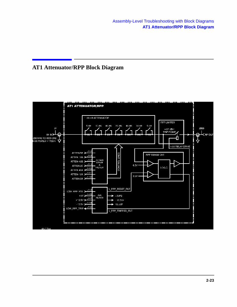
Assembly-Level Troubleshooting with Block DiagramsAT1 Attenuator/RPP Block Diagram
AT1 Attenuator/RPP Block Diagram
2-23

Assembly-Level Troubleshooting with Block DiagramsAT1 Attenuator/RPP Block Diagram
2-24

A7 BASEBAND GENERATOR BLOCK DIAGRAM (OPTION IEH)
s
DAC
I DATA GENERATION
ANALOG FILTERS(NADC/PDCPHS GSM)
π
WRITE DATA
LATCH I CAL12
12FORMAT SELECT
CONTROL LOGIC
/4 CLK
FORMAT SELECT
CA ADDRESS & CONTROL
ICAL LATCHES
I /4 DQPS
(NADC, PHS,PDC)
π
ICONSTANT AMPL
(GMSK, GFSK)
ABUS
I OUT
P405
I OUT
PATH CONTROLLOGIC
I DACDATA
MODULATIONENABLE/SELECT
TO I-OUT
INT I MOD OUTP301-2
Q DATA GENERATION
WRITE DATA
LATCH Q CAL12 Q
CAL LATCHES
Q OUT
π
π
12FORMAT SELECT
/4 CONTROL LOGIC
/4 CLK
FORMAT SELECT
CA ADDRESS & CONTROL
Q /4 DQPSKπ
QCONSTANT AMPL
(GMSK, GFSK)
Q DACDATA
MODULATIONENABLE/SELECT
MODINVERT DAC
ANALOG FILTERS(NADC/PDCPHS GSM)
ABUS
PATH CONTROLLOGIC
MOD INVERT
P404
Q OUTTO I-OUT
INT Q MOD OUTP301-53
ABUS
BURST
BURST MOD
BURST MODSWITCH
ANDFILTERS
BURSTPLS
BURSTCONTROL LOGIC
P301-59P301-80
L DCC ALT PWR SEL
INTL ALC HOLD
BURST PULSE
BURST ENVELOPE
P301-31
P301-30
P301-57
+PTAT
EEPROM
DATA
LATCHEDADDRESS
LATCHEDDATA
CONTROLLOGIC
DIGITAL INTERFACE
P301-33EXT SELECT
L EXT STROBEP301-82
P301-83EXT RD L WR
EXT RESETP301-32
P301-24IAB0
IAB1P301-74
P301-25IAB2
IAB3P301-26
P301-76IAB4
IAB5P301-27
P301-77IAB6
IAB7P301-78
P301-29IAB8
IAB9P301-79
P301-36IAB10
READ/LWRITE
STROBE
SELECT
RESET
A0
A1
A2
A3
A4
A5
A6
A7
A8
A9
A10
P301-19EXT_DO
EXT_D1P301-20
P301-70EXT_D2
EXT_D3P301-21
P301-71EXT_D4
EXT_D5P301-72
P301-23EXT_D6
P301-73EXT_D7
D0
DIG BUS INT(PLL UNLOCKED)
D1
D2
D3
D4
D5
D6
D7
SELECT
CLKPLL BUF BIT CLK
PLL LOCK SIG
PLL REF
π
DATA GENERATION CONTROL
LOOPCOUNT
&DIFF
ENCODE
INTERNALCLK
MASTER CLOCK
BIT CLOCK INV
BUFFERED DATA
SYMBOL SYNC INV
PMF CONTROL
CONTROLLOGIC
BURSTCONTROL LOGIC
BURST PLS
MOD INVERT
CAL ENABLE
LATCH I CAL
LATCH Q CAL
PLL GAIN
EXT REF ENABLE
/4 PMF ENABLE
CA PMF ENABLE
VCO ENABLE
EVENT SELECT
PATHCONTROL LOGIC
PMF CONTROL
FORMAT SELECT
SUB I CLK
BIT CLK INV
LATCH ADDRESS
L BURST
LATCH DATA
π /4 CLK
INT CLOCK
SUB I CLKS
PLL LOCK SIG
PATHCONTROL
LOGIC
π
CA ADDRESS & CONTROL
/4 CONTROL LOGIC
REF
MASTER CLOCK PLL
ABUS
PLL TUNE
PLL_ TUNE 160 TO 320 MHz
MASTER CLOCK
20 TO 40 MHz
VCOENABLE
DIG BUS INT(PLL UNLOCKED)
LOOP FILTER&
LEAD/LAG
KT
PLL BUF BIT CLOCK
BIT CLOCK INV
CLK OUT P300-14 TO DATACLK OUT
T DATA OUT P300-12 TO DATA OUT
BUFFERED DATA
RC TIMECONSTANT
ABUS
DATA
SYMBOL SYNC INV
T SYNC OUT P300-12 TO SYMBOLSYNC OUT
TT
L BURST
Φ PLL DIVIDERS
VCO
POWER SUPPLY INPUTS
+15V
+10 VREF
ABUS -1 VREF
-1 VREF
+32VP301-9
P301-14,64
P301-16,66
P301-17,67
P301-12
P301-62
P301-13,63
P301-1,7,54,56
P301-22,28,34,40,46,69,75,81,
87,93 ,99
+5VA
+5.2V
-5.2V
-5V
-15V
ANALOG COMMON
DIGITAL COMMON
+10VREF
INTERNAL DATA GENERATORINTERNAL DATAGENERATOR
(PATTERN RAM=1MINTERNAL SYNC
INTERNAL DATA
PATTERN TRIG
FROM PATTERN TRIG IN
P300-4
PLL BUF BIT CLK
EVENT SELECT
INTERNAL BURST
INTERNAL ALT POWER
P300-10EVENT 2 TO EVENT 2
EVENT 1 TO EVENT 1P300-8
DATA SWITCH
REFERENCE
REF SELECT&
DIVIDE
10 MHz DIGP301-84FROM MOTHERBOARD
/CPU
13 MHzFROM 13 MHz IN
P403
DATA CLOCKFROM DATA CLOCK
CLOCSELECINT CLOCK
P103
FROM SYMBOL SYNC
FROMBURST GATE IN
DATASELEC
P100
DATAFROM DATA
INT DATA
SYMBOL SYNC
SYNCSELECINT SYNC
P101
P300-2
BURSSELEC
BURST GATE
INT BURST
A7 BASEBAND GENERATOR BLOCK DIAGRAM (OPTION IEH)k784a

Assembly-Level Troubleshooting with Block DiagramsA7 Baseband Generator Board Block Diagram (Option 1EH)
2-26

A7 BASEBAND GENERATOR BLOCK DIAGRAM (OPTIONS UN3 & UN4)
s
DAC
I DATA GENERATION
ANALOG FILTERS(NADC/TETRA/PDC,PHS,GSM)
π
WRITE DATA
LATCH I CAL12
12FORMAT SELECT
π/4 CONTROL LOGIC
/4 CLK
FORMAT SELECT
CA ADDRESS & CONTROL
ICAL LATCHES
I /4 DQPSK
(NADC,TETRA,PDC,PHS)
π
ICONSTANTAMPLITUDE
(GMSK, GFSKDECT)
ABUS
I OUT
P405
I OUT
PATH CONTROLLOGIC
I DACDATA
MODULATIONENABLE/SELECT
TO I-OUT
INT I MOD OUTP301-2
Q DATA GENERATION
WRITE DATA
LATCH Q CAL12 Q
CAL LATCHES
Q OUT
π
π
12FORMAT SELECT
/4 CONTROL LOGIC
/4 CLK
FORMAT SELECT
CA ADDRESS & CONTROL
Q /4 DQPSK
(NADC,TETRA,PDC,PHS)
π
QCONSTANT AMPLITUDE
(GMSK,GFSK,DECT)
Q DACDATA
MODULATIONENABLE/SELECT
MODINVERT DAC
ANALOG FILTERS(NADC/TETRA/PDC,PHS GSM)
ABUS
PATH CONTROLLOGIC
MOD INVERT
P404
Q OUTTO Q-OUT
INT Q MOD OUTP301-53
BURST MOD
EEPROM
DATA
LATCHEDADDRESS
LATCHEDDATA
CONTROLLOGIC
DIGITAL INTERFACE
IAB3P301-26
P301-33EXT SELECT
L EXT STROBEP301-82
P301-83EXT RD L WR
EXT RESETP301-32
P301-24IAB0
IAB1P301-74
P301-25IAB2
P301-76IAB4
IAB5P301-27
P301-77IAB6
IAB7P301-78
P301-29IAB8
IAB9P301-79
P301-36IAB10
READ/LWRITE
STROBE
SELECT
RESET
A0
A1
A2
A3
A4
A5
A6
A7
A8
A9
A10
P301-19EXT_DO
EXT_D1P301-20
P301-70EXT_D2
EXT_D3P301-21
P301-71EXT_D4
EXT_D5P301-72
P301-23EXT_D6
P301-73EXT_D7
D0
DIG BUS INT(PLL UNLOCKED)
D1
D2
D3
D4
D5
D6
D7
SELECT
CLKPLL CLK
PLL LOCK SIG
PLL REF
π
DATA GENERATION CONTROL
CONTROLLOGIC
BURSTCONTROL LOGIC
BURST PLS
MOD INVERT
CAL ENABLE
LATCH I CAL
LATCH Q CAL
PLL GAIN
EXT REF ENABLE
/4 PMF ENABLE
CA PMF ENABLE
VCO ENABLE
EVENT SELECT
PATHCONTROL LOGIC
PMF CONTROL
FORMAT SELECT
LBIT_CLK
LATCH ADDRESS
L_BURST
LATCH DATA
PMFCONTROL
LOGIC
LBIT_CLK
BBG_BIT_CLK
LDATA_CLK
REF
MASTER CLOCK PLL
160 T O 320 MHz
MASTER CLOCK
20 T O 40 MHz
VCOENABLE
Φ PLL DIVIDERS
VCOABUS
PLL T UNE
PLL_T UNE
P301-35DIG BUS INT(PLL UNLOCKED)
LOOP FILTER&
LEAD/LAG
P300-22
BBG_BIT_CLKP300-16
LOOPCOUNT
&DIFF
ENCODE
INTERNALCLKMASTER CLOCK
LBIT_CLK
BUFFERED DATA
SYMBOL SYNC INV
PMF CONTROL
π /4 CLK
SUB_ I_COUNT (3)
PLL LOCK SIG
SUB_I _COUNT (1)
π
CA ADDRESS & CONTROL
/4 CONTROL LOGIC
P300-22
P300-16
SUB_I_COUNT (1)
PLL_CLOCK
L_BURST
BUFFERED_DATA_IN
SYMBOL_SYNC_INV
ABUS
DATA
RC TIMECONSTANT
LDATA_CLK
ABUS
LCLK
ABUS
BURST
RC TIMECONSTANT
POWER SUPPLY INPUTS
+15V
+10 VREF
ABUS -1V_REF
-1 V_REF
+32VP301-9
P301-14,64
P301-16,66
P301-17,67
P301-12
P301-62
P301-13,63
P301-1,7,54,56
P301-22,28,34,40,46,69,75,81,
87,93 ,99
+5VA
+5.2V
-5.2V
-5V
-15V
ANALOG COMMON
DIGITAL COMMON
+10VREF
BURST MODSWITCH
ANDFILTERS
P301-80L_DCC_ALT_PWR_SEL
INTL_ALC_HOLD
BURST_PULSE
BURST_ENVELOPE
P301-31
P301-30
P301-57
BURSTENVELOPECONTROL
&RAM
ENVL_LATCH
LATCH_DATA
BURST_TC
MASTER_CLK
BURST_PLS
CONTROL LOGIC
DAC_EN
-IV_REF
ENVELOPEDATA
15
15
GENERATOR INTERFACE
REFERENCE
REF SELECT&
DIVIDE
10 MHz DIGP301-84FROM MOTHERBOARD
/CPU
13 MHzFROM 13 MHz IN
P403
P300-6 BURST_GATE
ADJ_TS_PWR_INP300-8
P300-10BB_DATA
SYMBOL_SYNCP300-12
P300-14EXT_CLK
14
12
10
8
6
BBG_INT_CLKP300-18
P300-20BBG_EN
20
18
22
16
A7 BASEBAND GENERATOR BLOCK DIAGRAM (OPTIONS UN3 & UN4)k7120a

Assembly-Level Troubleshooting with Block DiagramsA7 Baseband Generator Board Block Diagram (Options UN3 & UN4)
2-28

Assembly-Level Troubleshooting with Block DiagramsA8 Data Generator Board Block Diagram (Options UN3 & UN4)
A8 Data Generator Board Block Diagram (Options UN3 & UN4)
2-29

Assembly-Level Troubleshooting with Block DiagramsA8 Data Generator Board Block Diagram (Options UN3 & UN4)
2-30

POWER SUPPLY & GROUND INTERCONNECTS (1 OF 2)
s
POWER SUPPLY MOTHER BOARDHP-IB
C
DCOM DCOM DCOM
FILTER
FILTER
FILTER
FILTER
FILTER
SYNTHESIZER BOARD
P3-1,3,5,7,9
D
A
P2-23,26,27,28
P2-15,30
P2-1,16
P2-10,12,13,22
J43-12,16,18,19,20 P3-12,16,18,19,20
+9VF1
+9V
+9VF2P2-5,20
+12VF
+15VF
+10VREFP2-6,21
-12VF
-15VF
-10VREFP2-2,17
P3-17
PRE_LEVEL_DRIVE
+5VF
+5.2V
P42-14,29
+32VFP2-7
-5.2VP2-4,19
-6VF
J43-1,3,5,7,9
DGND
J42-23,26,27,28
J42-15,30
J42-1,16
ACOM
J42-10,12,13,22
ACOM
J42-5,20
+9V
J42-6,21
+15V
J42-2,17
-15V
J43-17
+5.2VD
J42-14,29
J42-7
-5.2V
J42-4,19
J42,-3,18 P2,-3,18
TER BOARD
1
10 MHz_GND
+15V_STBY
10_MHz_OUT
10_MHz_IN
DCOM
DGND
6,
7
4
5,28,51
OD
_RTN
_RTN
MOD
D_1
D_1_RTN
D_2
D_2_RTN
UT
-6V
+5.2VD
-5.2V
+9V
+32V
+15V
-15V
DCOM
ACOM
UT_RTN
C
C
J32-15,30 P2-15,30DCOM
REFERENCE BOARD
J32-1,16 P2-1,16ACOM
ACOM
DGND
J33-1,14,16 P3-1,4,14,16AMOD
ACOM
J31-1,2,3,11,12,14J32-10,12,13,22J32-23,27,28
NCACOM
P1-1,2,3,11,12,14P2-10,12,13,22P2-23,27,28
+5.2VD
J32-14,29+5VD
Filter
Filter
D
D
A
A
+5.2VD
+5VA
J32-3,18NC
-6V
P2-3,18
P2-4,19
-5.2VFilter - 5VF
-5.2V
J32-4,19
+32VFilter
J32-7
J32-5,20NC
P2-5,20
+32VF
+32V
P2-4,19Filter
J32-4,19
P2-14,29
P2-7
+15V+15VF
J32-6,21
+10VREF
P2-6,21+14V
+15VD
+15V
-15V-15VF
J32-7,17 P2-7,17-14V
-15V
Filter -15V_SF
+15V_STBY
J32-26
+15V_STBY
P2-26
10_MHZ_IN EXT_REF_IN
J31-17 P1-17
MOD_OUT
P3-13 J33-13
MOD_OUT
MOD_OUT_RTN
P3-3 J33-3AMOD
EXT_MOD_1 EXT_MOD_1
J33-19 P3-19
J33-20 P3-20AMOD AMOD
EXT_MOD_2 EXT_MOD_2
J33-10 P3-10
EXT_MOD_2_RTN
J33-9 P3-9AMOD AMOD
EXT_MOD_2_RTN
10_MHZ_OUT10MHZ
P1-7 J31-710_MHZ_RTN
P1-16 J31-16ACOM
OUTPUT BOARD
(TO RP TYPE N) COHERENT CARRIER J5
J12-15,30
DGND
J12-1,16
ACOM
J11-7,11,12,13,14,16J12-8,9,12,13J12-26,27,28J13-1,2,3,5,7,9J13-11,12,13,14J13-16,18,20
A
D
ACOM
P2-14,29
+5.2VDFilter
+5VPR3
+5VF
+5VPR2
+5VPR
+5.2 V
R2215
R3215
R4215
J12-14,29
P2-3,18
-6V
-5.3VF2
-6VF
-6VF2J12-3,18
+32VNC
J12-7
P2-4,19
-5.2VNC
J12-4,19
-5.2 V
+30VF
A
A
(TO FP TYPE N) RF OUTPUT J6
-15VFilter -15V
-15VFJ12-2,17
P2-5,20
+9VFilter +9VF2
+9VF
J12-5,20
+15VFilter +15VF
J12-6,21
-15V
J13-10 P3-10A
EXT_I_MOD
J13-19
Filter
-5.3VF
EXT_I_Q_MOD EXT_I_Q_MOD
EXT_Q_MOD EXT_Q_MOD
J13-8
P3-4
PRE_LEVEL_DRIVE PRE_LEVEL_DRIVE
J13-4
P2-15,30
P2-1,16
P1-7,11,12,13,14,16P2-8,9,12,13P2-26,27,28P3-1,2,3,5,7,9P3-11,12,13,14P3-16,18,20
P2-7
P2-6,21
P2-2,17
EXT_I_ MOD
P3-19
P3-8
NC
+ 9V
DAUGHTER CARD CAGE
J6-2,3,12,13J6-2,3,12,13
+ 5.2 V+ 5.2 V
FILTERFILTER
DCOM
+5.2V
DCOM
FILTER
DCOM
+5.2VD
+5.2VD
+ 5.2 VD
+5.2VD
DCOM
FILTER
DCOM
FILTER
C1100p
C
C2100p
C
C347p
C
DCOM
DCOM
+5VPSF
ACOM
SW REG
ACOM
+5VPSF
DCOM
SW REG
DCOM
+5VPSF
ACOM
FILTER
C447p
C
ACOM
J6-4,5,14,15 J6-4,5,14,15
J6-6,16
ACOM
J6-6,16
ACOM
R1121
C
DCOM
ACOM
R110
DCOM
ACOM
J6-19 J6-19
+ 12 V + 12 V
J6-20 J6-20
+ 15 V + 15 V
+12V
ACOM
FILTER
ACOM(SEE NOTE 3)
+12V
ACOM
SW REG
ACOM
+12V
DCOM
LINEAR REG
ACOM
J6-18 J6-18
- 15 V - 15 V
ACOM
-15V
ACOM
LINEAR
LINEAR
REG
REG
+15V
ACOMACOM
C5100p
C
+15V
-15V
(FL LAMP +5.2V)
(FL LAMP RTN)
(RPG 5.2VD )
(RPG RTN)
+5.2VD
(LCD +5.2VD)
(LCD RTN)
-6V
-5.2V
(CONTROL VOLTAGE)
VLCD
ACOM
(FAN +12V)
(FAN RTN)
+32V
+9V
+12V
-12.5V
+15V_STBY
+12.5V
+15V
VDISP
-15V
(CONTROL VOLTAGE)
J6-17 J6-17
+ 15 V_STBY + 15 V_STBY
DAUGH
J1-37,87
J1-30,31,80,8
NC
J1-35,85
J1-83
J1-34,84
J1-32,82
J5-37,87
-6V
J5-30,31,80,81
+5.2VD
J5-35,85
-5.2V
J5-83
J5-34,84
+9V
+32V
J5-32,82
+15V
J1-36,86
J1-33
J1-98,100
J1-97
-15V
J5-36,86
J5-33
J5-98,100
10 MHz_GND
J5-97
+15V_STBY
10_MHz_IN
10_MHz_OUT
J5-99 J1-99
C
J1-43,47,49,9
J1-27,38,39,7J1-88,89,90J1-15,19,25J1-68,71,72,7
J1-57,63,69,7J1-4,10,16,22
DCOM
J5-43,47,49,96,
J5-57,63,69,75J5-4,10,16,22,28,51
ACOM
ACOM
(TO FP BNC)
J2I
(TO FP BNC)
J4EXT1
(TO FP BNC)
J5EXT2
(TO FP BNC)
J6LF OUTPUT
(TO FP BNC)
J3Q
EXT_I_M
EXT_I_Q
EXT_I_Q
C
EXT_Q_
C
EXT_MO
EXT_MO
C
EXT_MO
EXT_MO
C
MOD_O
MOD_O
C
POWER SUPPLY & GROUND INTERCONNECTS (1 OF 2)
k7129a

Assembly-Level Troubleshooting with Block DiagramsInterconnects Block Diagram - Power Supply and Ground (1 of 2)
2-32

RPG
J1-12
J1-8D
J20-12
J20-8
(RPG 5.2VD)
(RPG RTN)
LCD(BRIGHTNESS)
J19-1
J19-3
J19-2
(FL LAMP +5.2V)
(FL LAMP RTN)
(VDISP)
LCD(CONTRAST)
J21-5
J21-6
J21-7
(LCD +5.2VD)
(LCD RTN)
(VLCD)
FAN A/B
J16-17,1
J16-17,2 (BLACK)
(RED)
(FAN +12V)
(FAN RTN)
C
MIPPS ATTENUATOR
J1-15
J1-4
J14-15
J14-8
-5.2VD
ACOM
ACOM
+5V+5VF
+5V_RFI_FILT
Filter
Filter
J1-7
J1-14
J14-14
J14-13
+12.5V
-12.5V
+12.5VS
-12.5VS
+12.5V_RFI_FILT
-12.5V_RFI_FILT
+10VF
-10VF
+10VP
-10VP
Filter
Filter
MOTHER BOARD
TEST &DIAGNOSTICS
J23-J24,1,2,63,64 J25-3,5
J25-9
J23-J24,3,4,61,62
J23-26
DCOM
DCOM
+5.2VD
+12V
(RP BNC)10 MHz INJ12-A
(RP BNC)10 MHz OUTJ13-A
10_MHz_IN
10_MHz_OUT
J5-97
J5-98
J5-99
J5-100
10MHz_GND
10MHz_GND
10 MHz I/O
HP-IB RPCONNECTOR
DCOM
DCOM
SERIAL I/OINTERFACE
J18-6J26-10
J18-8J26-12
J18-10J26-14
J18-9J26-13
J18-7J26-11
DCOM
DCOM
+5.2VD
+32V
+15V
-15V
(RP BNC)TRIGGER INJ11-A
(RP BNC)TRIGGER OUTJ10-A
RP_TRIG_IN
RP_TRIG_OUT
TRIGGER_GND
TRIGGER_GND
TRIGGER I/O
TRIGGER_GND DCOM
R2
10
DCOM
(RP BNC)SWEEP OUTJ10-A
SWEEP_RAMP_OUT
SWEEP_GND
SWEEP RAMP
SWEEPRAMP
RS232 RPCONNECTOR
J8-5
J8-4
SERIAL_GND
DCOM
DCOM
+5.2VD
J8-PM1,PMH2
J7-12,18,19,20J7-21,22,23,24J7-PMH1,PMH2
DIGITAL CARD CAGEOPTION 1EH
+5.2VD
-5.2VD
P300-1,3,5,7,9,11,13,15
DATAGENERATOR
49,753,99
M
P1-1,7,54,56,56
M
P1-16,66,66
,67
+5V
+5V
+5A
A
D
+5D
Filter
Filter
4,9
,65
,64
+32V
+12V
+15V
2V
2V
5V
+32F
NC
+15F
Filter
Filter
,12
,62
-5V
-5V
-5F1
-5F2
Filter
Filter
P1-13,63,63
-15V5V-15FFilter
P1-14,64
P1-62
P1-9
P1-12
P1-17,67
P1-22,28,34P1-40,46,69,75P1-81,87,93,99
J1
J2
J3
C02
100p
DCOM
DCOM
(FP BNC)SYNCP101
(RP D Conn)DIGITAL MODINTERFACE
C
C
(FP BNC)DATAP100
(FP BNC)CLOCKP103
EXT_DATA
EXT_CLK
EXT_SYNC
DIGITAL CARD CAGEOPTION(S) UN3/UN4
POWER SUPPLY & GROUND INTERCONNECTS (2 OF 2)
BASEBANDGENERATOR
J1-J4,22,28,34J1-J4,40,46,69,75J1-J4,81,87,93,99
DCOM
P301-1,7,54,56J1-J4,1,7,54,56
ACOM
P301-16,66J1-J4,16,66
J1-J4,17,67
+5V
+5V
+5A
A
D
+5D
Filter
Filter
J1-J4,9
J1-J4,15,65
J1-J4,14,64
+32V
+12V
+15V
+32V
+12V
+15V
+32F
NC
+15F
Filter
Filter
J1-J4,12
J1-J4,62
-5V
-5V
-5F1
-5F2
Filter
Filter
P301-13,63J1-J4,13,63
-15V-15V-15FFilter
P301-14,64
P301-62
P301-9
P301-12
P301-17,67
P301-22,28,34P301-40,46,69,75P301-81,87,93,99
J1
J2
J3
C02
100p
DCOM
DCOM
(FP BNC)SYNCP101
(RP D Conn)DIGITAL MODINTERFACEP300-1,3,5,
7,9,11,13,15
C
C
(FP BNC)DATAP100
(FP BNC)CLOCKP103
EXT_DATA
EXT_CLK
EXT_SYNC
J1-J4,22,28,3J1-J4,40,46,6J1-J4,81,87,9
DCO
J1-J4,1,7,54
ACO
J1-J4,16
J1-J4,17
+5.2VD
J1-J
J1-J4,15
J1-J4,14
+3
+1
+1
J1-J4
J1-J4
-5.2VD
J1-J4,13
-1
BASEBANDGENERATOR
J1-J4,22,28,34J1-J4,40,46,69,75J1-J4,81,87,93,99
DCOM
P301-1,7,54,56J1-J4,1,7,54,56
ACOM
P301-16,66J1-J4,16,66
J1-J4,17,67
+5.2VD+5V
+5V
+5A
A
D
+5D
Filter
Filter
J1-J4,9
J1-J4,15,65
J1-J4,14,64
+32V
+12V
+15V
+32V
+12V
+15V
+32F
NC
+15F
Filter
Filter
J1-J4,12
J1-J4,62
-5.2VD-5V
-5V
-5F1
-5F2
Filter
Filter
P301-13,63J1-J4,13,63
-15V-15V-15FFilter
P301-14,64
P301-62
P301-9
P301-12
P301-17,67
P301-22,28,34P301-40,46,69,75P301-81,87,93,99
sk7130a
POWER SUPPLY & GROUND INTERCONNECTS (2 OF 2)

Assembly-Level Troubleshooting with Block DiagramsInterconnects Block Diagram - Power Supply and Ground (2 of 2)
2-34

MO
DU
LATIO
N A
ND
SIGN
AL IN
TERCON
NECTS (1 of 2)
MO
DU
LATIO
N A
ND
SIGN
AL IN
TERCON
NECTS (1 of 2)
DAUGHTER BOARD MOTHER BOARDD ESYNTHESIZER BOARDA
J1-11 J5-11J41-7
J1-5 J5-5J41-18
J1-13 J5-13J41-4
J1-14 J5-14J41-1
J1-59 J5-59J41-12
J1-8 J5-8J41-13
J1-64 J5-64J41-3
J1-58 J5-58J41-14
J41-20 J1-54 J5-54
J1-15 J5-15
J1-61 J5-61J41-8
J1-62 J5-62J41-6
J1-6 J5-6J41-16
J1-12 J5-12J41-5
J1-7 J5-7J41-15
FMDATA5
FMDATA3
FMDATA4
FMDATA6
FMDATA7
FMDATA8
FMDATA11
FMDATA9
FMDATA10
FMDATA12
FMDATA13
FMDATA14
FMDATA15
COUNTER
MOD_STROBE
FM_MOD
FM_MOD_RTN
P1-11
P3-15
P1-2
P3-14
FMDATA5
FMDATA3
FMDATA4
FMDATA6
FMDATA7
FMDATA8
FMDATA11
FMDATA9
FMDATA10
FMDATA12
FMDATA13
FMDATA14
FMDATA15
MOD_STRB
P1-8
P1-7
P1-18
P1-6
P1-16
P1-5
P1-1
P1-15
P1-4
P1-12
P1-13
P1-3
P1-14
P1-20
J1- J4,47
J1- J4,91
J1- J4,95
J1- J4,90
J1- J4,96
J1- J4,88
J1- J4,37
J1- J4,92
J1- J4,43
J1- J4,38
J1- J4,44
J1- J4,97
J1- J4,86
J1- J4,41
J1- J4,89
J1- J4,45
J1- J4,39
J1- J4,94
FMDATA0
FMDATA1
FMDATA2
FMDATA5
FMDATA3
FMDATA4
FMDATA6
FMDATA7
FMDATA8
FMDATA11
FMDATA9
FMDATA10
FMDATA12
FMDATA13
FMDATA14
FMDATA15
COUNTER
MOD_STROBE
NCR34.22 k
+5.2 VD
J1-55 J5-55J41-19
J1-60 J5-60J41-9
J1-56 J5-56J41-17
FMDATA0
FMDATA1
FMDATA2
FMDATA0
FMDATA1
FMDATA2
P1-19
P1-9
P1-17
J1-26 J5-26J42-25
J1-23 J5-23J42-24
J1-20 J5-20J41-17
SYNTH_EN SYNTH_EN SYNTH_EN
SYNTH_CLK SYNTH_CLK SYNTH_CLK
SYNTH_DATA SYNTH_DATA SYNTH_DATA
P2-25
P2-24
P2-11
J43-15
J41-2
J43-14
J41-11
FM_MOD
FM_MOD_RTN
10_MHz_SYNTH
10_MHz_SYNTH_RTN
J1- J4,3
J1- J4,52
J1- J4,53
J1- J4,57
J1- J4,59
J1- J4,58
J1- J4,8
J1- J4,31
J1- J4,80
L
J1- J4,2
FM_MOD
FM_MOD_RTN
J31-5
J33-12
J31-6
J33-11
J1- J4,55
J1- J4,6
J1- J4,30
J5-24
REF_EN
REF_CLKJ1-24J32-25
10_MHz_SYNTH
10_MHz_SYNTH_RTN
REF_EN
REF_CLK
REFERENCE BOARDREFERENCE BOARDBB
FM_MOD_RTN
FM_MOD
P3-12
P1-5
P1-6
P2-25
P3-11
10_MHz_SYNTH
10_MHz_SYNTH_RTN
REF_EN
REF_CLK
AMOD
R246.4
sk7131a
OUTPUT BOARDC
INT _I _MOD P3-15
+PTAT
BURST ENVELOPE
INT_Q_MOD
FADE ENVELOPE
L _ALC _HOLD
P1-6
P1-15
P3-6
P1-3
P1-17
P2-22
L _ALT_ PWR_ SEL
P2-10
P2-25
P2-24
A
INT I-Q RTN
P3-17A J5-45
J5-94
J5-95
J5-42
J5-40
BURST_ENVELOPE
+PTAT
INT_Q_MOD_RTN
INT_Q_MOD
INT_I_MOD_RTN
INT_I_Q_RTN
J1-45
INT_I_Q_RTN
J1-94
J13-17
INT_Q_MOD
J1-95J13-6
BURST_ENVELOPE
+PTAT
J1-42
J1-40
J11-6
J11-15
J31-19
1_GHz_REF_OSC1_GHz_REF_OSC
1_GHz_RTN1_GHz_RTN
LIN_AM_RTNLIN_AM_RTN
LIN_AM_MODLIN_AM_MOD
J31-5
J11-8,9,10,18,20
J31-6
J11-19
1_GHz_REF_OSC
NC
P1-2
P1-19
P1-8,9,10,18,20
P1-1
J5-41
J5-91
J5-17
L_ALT_PWR_SEL
J5-29
FADE_ENVELOPE
ALC_GND
L_ALC_HOLD
+5.2VD
TRIG_INT
L_DCC_ALT_PWR_SE
DCOM
R11.96 k
MUX
FADE_ENVELOPE
J1-41J11-17
ALC_GND
J1-91J11-3
L_ALC_HOLD
J1-17J12-22
L_ALT_PWR_SEL
J1-29J12-10
+5.2 VD
J5-76
J5-73
OUT_EN
OUT_CLK
OUT_DATA
J1-76J12-25
J1-73J12-24
OUT_EN
OUT_CLK
OUT_DATA
OUT_EN
OUT_CLK
OUT_DATA
J13-15
INT_I_MOD
J5-44
INT_I_MOD
J1-44
J33-18
J31-8,9,10,18,20
J33-17
1_GHz_RTN
LIN_AM_RTN
LIN_AM_MOD
J5-46
J5-48
J5-79
AUD_2
AUD_1
BURST_PULSE
AUD_2
J1-46J33-2AUD_1
J1-48J33-5
BURST_PULSE
J1-79J33-8
J5-21
J5-18
J5-50
REF_DATA
INT_MOD
J1-21J32-24
J1-18J33-11
REF_DATA
INT_MOD
J1-50J33-6
AUD_1
BURST_PULSE
AUD_2
P3-5
P3-2
P3-8
P3-17
P3-18
P1-8,9,10,18,20
P1-19
P2-24
P3-11
P3-6
1_GHz_REF_OSC
1_GHz_RTN
LIN_AM_RTN
LIN_AM_MOD
REF_DATA
INT_MOD
P2-11 J5-70J1-70J12-11

Assembly-Level Troubleshooting with Block DiagramsInterconnects Block Diagram - Modulation and Signal (1 of 2)
2-36

MO
DU
LATIO
N A
ND
SIGN
AL IN
TERCON
NECTS (2 of 2)
MO
DU
LATIO
N A
ND
SIGN
AL IN
TERCON
NECTS (2 of 2)
sk7
13
2a
DIGITAL CARD CAGE (OPTION 1EH)F
J1- J4,47
J1- J4,91
J1- J4,95
J1- J4,90
J1- J4,96
J1- J4,88
J1- J4,37
J1- J4,92
J1- J4,43
J1- J4,38
J1- J4,44
J1- J4,97
J1- J4,86
J1- J4,41
J1- J4,89
J1- J4,45
J1- J4,39
J1- J4,94
NC
NC
NC
NC
NC
NC
NC
NC
NC
NC
NC
NC
NC
NC
NC
NC
NC
NC
BASEBANDGENERATORBOARD
G
DIGITAL CARD CAGE (OPTIONS UN3 & UN4)F
J1- J4,47
J1- J4,91
J1- J4,95
J1- J4,90
J1- J4,96
J1- J4,88
J1- J4,37
J1- J4,92
J1- J4,43
J1- J4,38
J1- J4,44
J1- J4,97
J1- J4,86
J1- J4,41
J1- J4,89
J1- J4,45
J1- J4,39
J1- J4,94
NC
NC
NC
NC
NC
NC
NC
NC
NC
NC
NC
NC
NC
NC
NC
NC
NC
NC
BASEBANDGENERATORBOARD
G DATAGENERATORBOARD
H
BURST_GATE
P3-6
ADJ_TS_PWR_IN
BB_DATA
SYMBOL_SYNC
EXT_CLK
BBG_BIT_CLK
BBG_INT_CLK
BBG_EN
SUB_I_COUNT
P3-8
P3-10
P3-12
P3-14
P3-16
P3-18
P3-20
P3-22
NC
NC
NC
EVENT 1
EVENT 2
BURSTGATE IN
PATTERNTRIG IN
EXT_BURST
PATTERN_TRIG
ALT_PWR_IN
EVENT (1) OUT
USER_DATA_EN
P2-2
P2-4
P2-6
P2-8
P2-10
P2-1,3,5,79,11,13,15
10K 100pf
P301-3
P301-52
J1- J4,3
J1- J4,52
J1- J4,53
J1- J4,57
J1- J4,59
INT_Q_MOD_RTN
INT_Q_MOD
INT_I_MOD_RTN
P301-53
BURST_ENVELOPE
+PTAT
P301-57
P301-59
ACOM
ACOM
NC
NC
INTL_ALC_GATE
P301-31
L_ALT_PWR_SEL
P301-80
J1- J4,58
J1- J4,8
J1- J4,31
J1- J4,80
INT_I_MOD
P301-2J1- J4,2
BURST_PULSE
P301-30
NC
NC
J1- J4,55
J1- J4,6
J1- J4,30
P301-3
P301-52
J1- J4,3
J1- J4,52
J1- J4,53
J1- J4,57
J1- J4,59
INT_Q_MOD_RTN
INT_Q_MOD
INT_I_MOD_RTN
P301-53
BURST_ENVELOPE
P301-57
ACOM
ACOM
NC
NC
NC
INTL_ALC_HOLD
P301-31
L_ALT_PWR_SEL
P301-80
J1- J4,58
J1- J4,8
J1- J4,31
J1- J4,80
INT_I_MOD
P301-2J1- J4,2
BURST_PULSE
P301-30
NC
NC
J1- J4,55
J1- J4,6
J1- J4,30
BURST_GATE
P300-6
ADJ_TS_PWR_IN
BB_DATA
SYMBOL _SYNC
P300-8
P300-10
P300-12
BBG_INT_CLK
BBG_EN
SUB_I_COUNT
P300-18
P300-20
P300-22
EXT_CLK
BBG_BIT_CLK
P300-14
P300-16
RE
AR
PA
NE
L{

Assembly-Level Troubleshooting with Block DiagramsInterconnects Block Diagram - Modulation and Signal (2 of 2)
2-38

3 Replaceable Parts
This chapter provides important ordering information and lists the part numbers for the various replaceable parts, kits, and accessories available for your signal generator. This chapter is also useful for locating and identifying assemblies and cables.
3-1

Replaceable PartsOrdering Information
Ordering Information
To order a part listed in the replaceable parts lists:
1. Determine the part number.
2. Determine the quantity required.
3. Mail this information to the nearest Hewlett-Packard office or, in the U.S., call the hotline number listed in the following section.
To order a part not listed in the replaceable parts lists:
1. Note the instrument model number.
2. Note the serial number and options, if any (see rear panel).
3. Describe the part.
4. Describe the function of the part.
5. Determine the quantity required.
6. Mail this information to the nearest Hewlett-Packard office or, in the U.S., call the hotline number listed in the following section.
Call (800) 227-8164 to Order Parts Fast (U.S. Only)
When you have gathered the information required to place an order, contact Hewlett-Packard’s direct ordering team by calling the toll-free hotline number shown above. Orders may be placed Monday through Friday, 6 AM to 5 PM (Pacific Standard Time).
The parts specialists have direct on-line access to replacement parts inventory corresponding to the replaceable parts lists in this manual. Four day delivery time is standard; there is a charge for hotline one-day delivery.
This information applies to the United States only. Outside the United States, you must contact the nearest HP sales and service office. (Refer to Table 3-1.)
3-2

Replaceable PartsOrdering Information
Table 3-1. Hewlett-Packard Sales and Service Offices
US FIELD OPERATIONS
HeadquartersHewlett-Packard Company19320 Pruneridge AvenueCupertino, CA 95014, USA(800) 752-0900Atlanta AnnexHewlett-Packard Co.2124 Barrett Park DriveKennesaw, GA 30144(404) 648-0000
California, NorthernHewlett-Packard Co.301 E. EvelynMountain View, CA 94041(415) 694-2000IllinoisHewlett-Packard Co.5201 Tollview DriveRolling Meadows, IL 60008(708) 255-9800
California, SouthernHewlett-Packard Co.1421 South Manhattan Ave.Fullerton, CA 92631(714) 999-6700New JerseyHewlett-Packard Co.150 Green Pond RoadRockaway, NJ 07866(201) 586-5400
ColoradoHewlett-Packard Co.24 Inverness Place, EastEnglewood, CO 80112(303) 649-5512TexasHewlett-Packard Co.930 E. Campbell Rd.Richardson, TX 75081(214) 231-6101
EUROPEAN FIELD OPERATIONS
HeadquartersHewlett-Packard S.A.150, Route du Nant-d’Avril1217 Meyrin 2/GenevaSwitzerland(41 22) 780.8111
FranceHewlett-Packard France1 Avenue Du CanadaZone D’Activite De CourtaboeufF-91947 Les Ulis CedexFrance(33 1) 69 82 60 60
GermanyHewlett-Packard GmbHHewlett-Packard Strasse61352 Bad Homburg v.d.HGermany(49 6172) 16-0
Great BritainHewlett-Packard Ltd.Eskdale Road, Winnersh TriangleWokingham, Berkshire RG41 5DZEngland(44 734) 696622
INTERCON FIELD OPERATIONS
HeadquartersHewlett-Packard Company3495 Deer Creek Rd.Palo Alto, CA 94304-1316(415) 857-5027JapanHewlett-Packard Japan, Ltd.1-27-15 Yabe, SagamiharaKanagawa 229, Japan(81 427) 59-1311
AustraliaHewlett-Packard Australia Ltd.31-41 Joseph StreetBlackburn, Victoria 3130(61 3) 895-2895SingaporeHewlett-Packard Singapore (Pte.) Ltd. 150 Beach Road#29-00 Gateway WestSingapore 0718(65) 291-9088
CanadaHewlett-Packard (Canada) Ltd.17500 South Service RoadTrans-Canada HighwayKirkland, Quebec H9J 2X8Canada(514) 697-4232TaiwanHewlett-Packard Taiwan8th Floor, H-P Building337 Fu Hsing North RoadTaipei, Taiwan(886 2) 712-0404
ChinaChina Hewlett-Packard Co.38 Bei San Huan X1 RoadShuang Yu ShuHai Dian DistrictBeijing, China(86 1) 256-6888
3-3
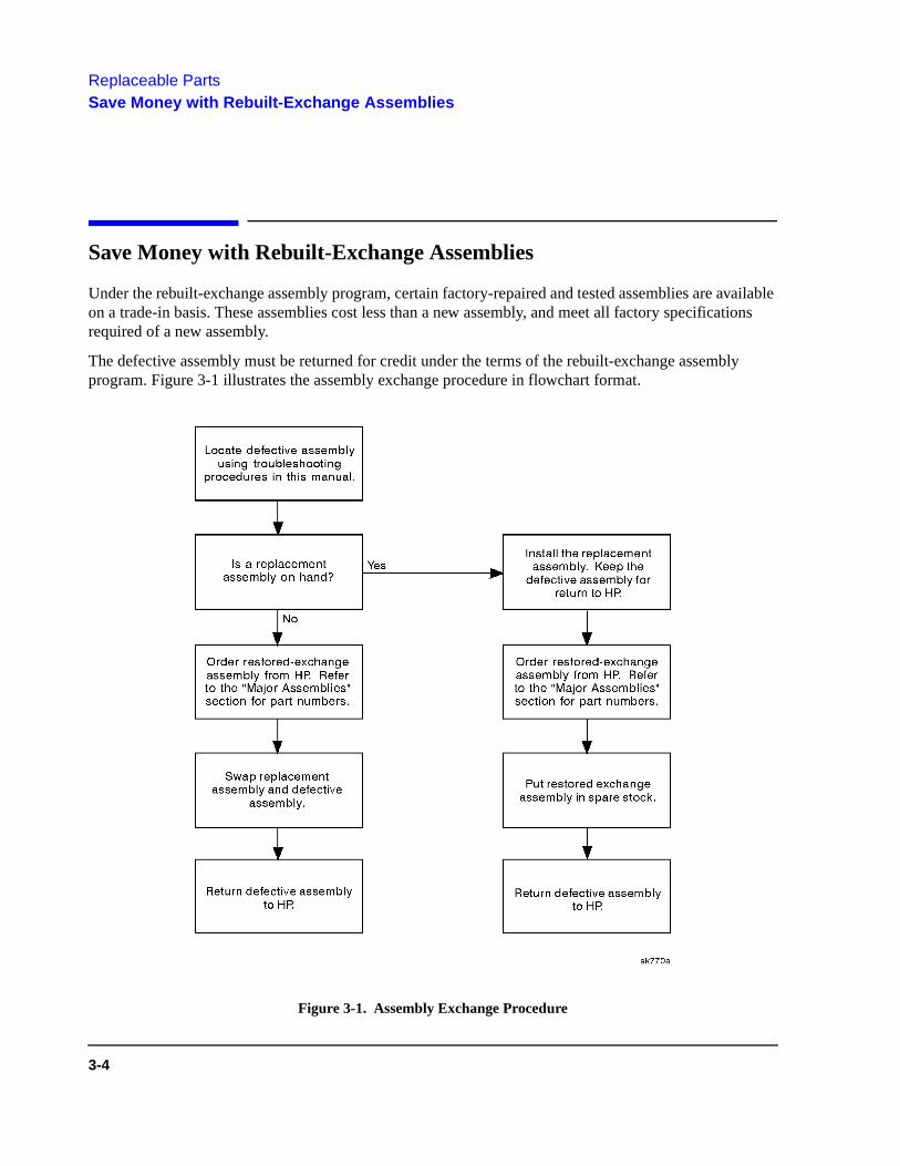
Replaceable PartsSave Money with Rebuilt-Exchange Assemblies
Save Money with Rebuilt-Exchange Assemblies
Under the rebuilt-exchange assembly program, certain factory-repaired and tested assemblies are available on a trade-in basis. These assemblies cost less than a new assembly, and meet all factory specifications required of a new assembly.
The defective assembly must be returned for credit under the terms of the rebuilt-exchange assembly program. Figure 3-1 illustrates the assembly exchange procedure in flowchart format.
Figure 3-1. Assembly Exchange Procedure
3-4

Replaceable PartsSave Money with Rebuilt-Exchange Assemblies
Shipping the Defective Assembly Back to Hewlett-Packard1. When the rebuilt assembly is received, be careful not to damage the box in which it was shipped. You will use that
box to return the defective assembly. The box you receive will contain the following:
• The rebuilt assembly• An exchange assembly failure report• A return address label
2. Complete the failure report.
3. Place the failure report and the defective assembly in the box. Be sure to remove the enclosed return address label.
4. Seal the box with tape.
If you are inside the United States, stick the preprinted return address label over the label that is already on the box and return box to HP. (HP pays postage on boxes mailed within the United States.)
If you are outside the USA, do not use the return address label; instead, address box to the nearest HP sales and service office. (Refer to Table 3-1.)
3-5
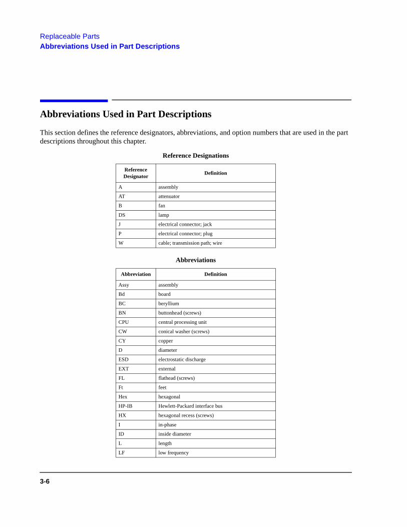
Replaceable PartsAbbreviations Used in Part Descriptions
Abbreviations Used in Part Descriptions
This section defines the reference designators, abbreviations, and option numbers that are used in the part descriptions throughout this chapter.
Reference Designations
Reference Designator
Definition
A assembly
AT attenuator
B fan
DS lamp
J electrical connector; jack
P electrical connector; plug
W cable; transmission path; wire
Abbreviations
Abbreviation Definition
Assy assembly
Bd board
BC beryllium
BN buttonhead (screws)
CPU central processing unit
CW conical washer (screws)
CY copper
D diameter
ESD electrostatic discharge
EXT external
FL flathead (screws)
Ft feet
Hex hexagonal
HP-IB Hewlett-Packard interface bus
HX hexagonal recess (screws)
I in-phase
ID inside diameter
L length
LF low frequency
3-6
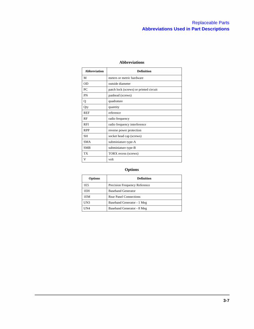
Replaceable PartsAbbreviations Used in Part Descriptions
M meters or metric hardware
OD outside diameter
PC patch lock (screws) or printed circuit
PN panhead (screws)
Q quadrature
Qty quantity
REF reference
RF radio frequency
RFI radio frequency interference
RPP reverse power protection
SH socket head cap (screws)
SMA subminiature type-A
SMB subminiature type-B
TX TORX recess (screws)
V volt
Options
Options Definition
1E5 Precision Frequency Reference
1EH Baseband Generator
1EM Rear Panel Connections
UN3 Baseband Generator - 1 Meg
UN4 Baseband Generator - 8 Meg
Abbreviations
Abbreviation Definition
3-7

Replaceable PartsMajor Assemblies
Major Assemblies
3-8

Replaceable PartsMajor Assemblies
Top View
Reference Designator
HP Part Number Qty Description
A4 0950-2929 1 Assy-Power Supply
3-9

Replaceable PartsMajor Assemblies
Top View
A7 E4400-60005 1 Bd Assy-Baseband Generator (Option 1EH)
A7 E4400-69005 Exchange Bd Assy-Baseband Generator (Option 1EH)
A7 E4400-60048 1 Bd Assy-Baseband Generator (Options UN3, UN4)
A7 E4400-69048 Exchange Bd Assy-Baseband Generator (Options UN3, UN4)
A8 E4400-60043 1 Bd Assy-Data Generator, 1 Meg (Option UN3)
A8 E4400-69043 Exchange Bd Assy-Data Generator, 1 Meg (Option UN3)
A8 E4400-60057 1 Bd Assy-Data Generator, 8 Meg (Option UN4)
A8 E4400-69057 Exchange Bd Assy-Data Generator, 8 Meg (Option UN4)
A14 E4400-60001 1 Bd Assy-CPU/Mother
A14 E4400-69001 Exchange Bd Assy-CPU/Mother
A14BT1 1420-0338 1 Battery-Lithium
AT1 E4400-60007 1 Assy-Electronic Attenuator/RPP
AT1 E4400-69007 Exchange Assy-Electronic Attenuator/RPP
B1 3160-1040 1 Assy-Fan, Small
B2 E4400-60062 1 Kit-Fan, Large (includes 2 foam strips)
Top View
Reference Designator
HP Part Number Qty Description
3-10

Replaceable PartsMajor Assemblies
Right Side View
Reference Designator
HP Part Number Qty Description
A9 E4400-60003 1 Bd Assy-Output
3-11

Replaceable PartsMajor Assemblies
Right Side View
A9 E4400-69003 Exchange Bd Assy-Output
A11 E4400-60010 1 Bd Assy-Reference, TCXO
A11 E4400-69010 Exchange Bd Assy-Reference, TCXO
A11 E4400-60009 1 Bd Assy-Reference, OCXO (Option 1E5)
A11 E4400-69009 Exchange Bd Assy-Reference, OCXO (Option 1E5)
A12 E4400-60002 1 Bd Assy-Synthesizer/Doubler
A12 E4400-69002 Exchange Bd Assy-Synthesizer/Doubler
A15 E4400-60011 1 Bd Assy-Daughter
Right Side View
Reference Designator
HP Part Number Qty Description
3-12
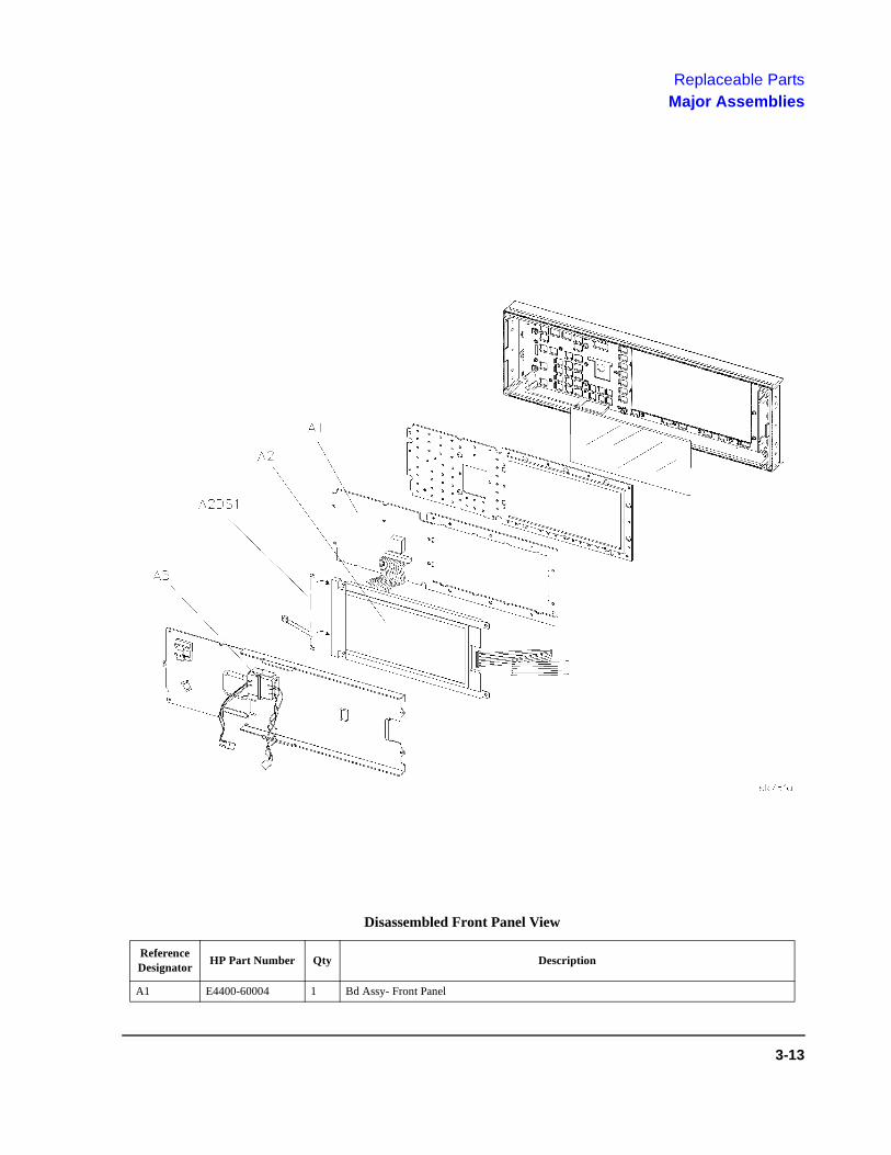
Replaceable PartsMajor Assemblies
Disassembled Front Panel View
Reference Designator
HP Part Number Qty Description
A1 E4400-60004 1 Bd Assy- Front Panel
3-13

Replaceable PartsMajor Assemblies
Disassembled Front Panel View
A2 1990-1910 1 Assy-Display
A2DS1 1513-5204 1 Lamp-Fluorescent
A3 0950-3093 1 Assy-Inverter
Disassembled Front Panel View
Reference Designator
HP Part Number Qty Description
3-14
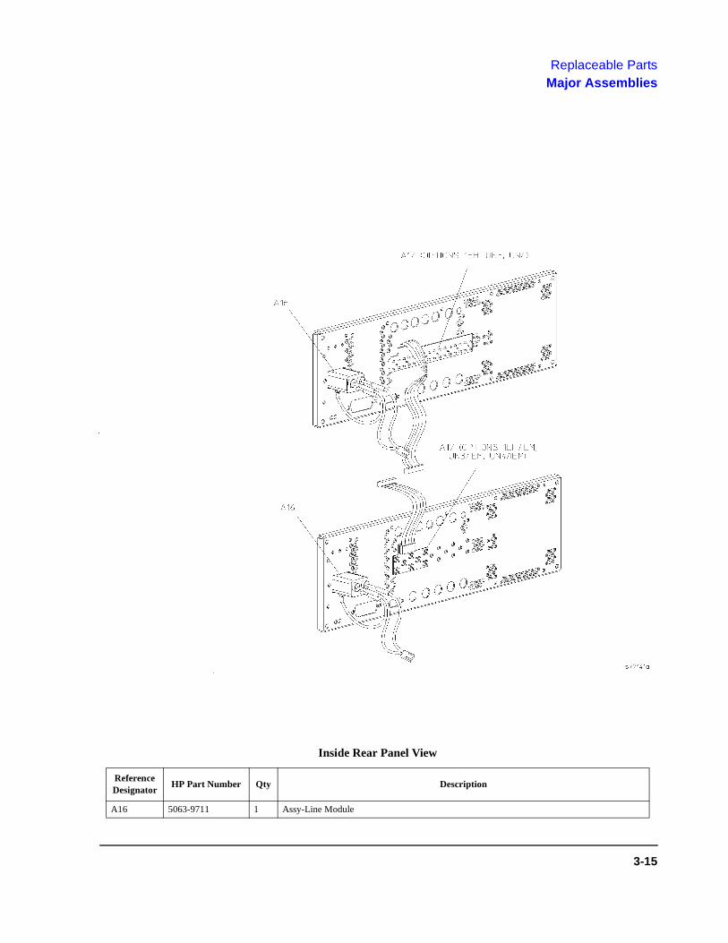
Replaceable PartsMajor Assemblies
Inside Rear Panel View
Reference Designator
HP Part Number Qty Description
A16 5063-9711 1 Assy-Line Module
3-15
Replaceable PartsMajor Assemblies
Inside Rear Panel View
A17 E4400-60044 1 Bd Assy-Rear Panel Interface (Options 1EH, UN3, UN4)
A17 E4400-60045 1 Bd Assy-Rear Panel Interface (Options 1EH/1EM, UN3/1EM, UN4/1EM)
Inside Rear Panel View
Reference Designator
HP Part Number Qty Description
3-16
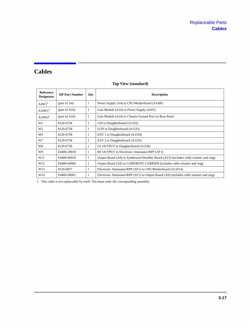
Replaceable PartsCables
Cables
Top View (standard)
Reference Designator
HP Part Number Qty Description
A4W11
1. This cable is not replaceable by itself. You must order the corresponding assembly.
(part of A4) 1 Power Supply (A4) to CPU/Motherboard (A14J6)
A16W11 (part of A16) 1 Line Module (A16) to Power Supply (A4J1)
A16W21 (part of A16) 1 Line Module (A16) to Chassis Ground Post on Rear Panel
W1 8120-6758 1 I IN to Daughterboard (A15J2)
W2 8120-6758 1 Q IN to Daughterboard (A15J3)
W6 8120-6758 1 EXT 1 to Daughterboard (A15J4)
W7 8120-6758 1 EXT 2 to Daughterboard (A15J5)
W8 8120-6758 1 LF OUTPUT to Daughterboard (A15J6)
W9 E4400-20018 1 RF OUTPUT to Electronic Attenuator/RPP (AT1)
W11 E4400-60059 1 Output Board (A9) to Synthesizer/Doubler Board (A12) (includes cable retainer and ring)
W12 E4400-60060 1 Output Board (A9) to COHERENT CARRIER (includes cable retainer and ring)
W13 8120-6837 1 Electronic Attenuator/RPP (AT1) to CPU/Motherboard (A14J14)
W14 E4400-60061 1 Electronic Attenuator/RPP (AT1) to Output Board (A9) (includes cable retainer and ring)
3-17

Replaceable PartsCables
Top View (standard)
3-18

Replaceable PartsCables
Top View (Option 1EH)
Reference Designator
HP Part Number Qty Description
A4W11
1. This cable is not replaceable by itself. You must order the corresponding assembly.
(part of A4) 1 Power Supply (A4) to CPU/Motherboard (A14J6)
A16W11 (part of A16) 1 Line Module (A16) to Power Supply (A4J1)
A16W21 (part of A16) 1 Line Module (A16) to Chassis Ground Post on Rear Panel
A17W11 (part of A17) 1 Rear Panel Interface Board (A17) to Baseband Generator (A7P300)
W1 8120-6758 1 I IN to Daughterboard (A15J2)
W2 8120-6758 1 Q IN to Daughterboard (A15J3)
W3 8120-5401 1 DATA to Baseband Generator (A7P100)
W4 8120-5401 1 DATA CLOCK to Baseband Generator (A7P103)
W5 8120-5401 1 SYMBOL SYNC to Baseband Generator (A7P101)
W6 8120-6758 1 EXT 1 to Daughterboard (A15J4)
W7 8120-6758 1 EXT 2 to Daughterboard (A15J5)
W8 8120-6758 1 LF OUTPUT to Daughterboard (A15J6)
W9 E4400-20018 1 RF OUTPUT to Electronic Attenuator/RPP (AT1)
W11 E4400-60059 1 Output Board (A9) to Synthesizer/Doubler Board (A12) (includes cable retainer and ring)
W12 E4400-60060 1 Output Board (A9) to COHERENT CARRIER (includes cable retainer and ring)
W13 8120-6837 1 Electronic Attenuator/RPP (AT1) to CPU/Motherboard (A14J14)
W14 E4400-60061 1 Electronic Attenuator/RPP (AT1) to Output Board (A9) (includes cable retainer and ring)
W15 8120-5055 1 Baseband Generator (A7P403) to 13 MHz
W16 8120-5055 1 Baseband Generator (A7P404) to Q OUT
W17 8120-5055 1 Baseband Generator (A7P405) to I OUT
3-19

Replaceable PartsCables
Top View (Option 1EH)
3-20

Replaceable PartsCables
Top View (Options UN3 & UN4)
Reference Designator
HP Part Number Qty Description
A4W11
1. This cable is not replaceable by itself. You must order the corresponding assembly.
(part of A4) 1 Power Supply (A4) to CPU/Motherboard (A14J6)
A16W11 (part of A16) 1 Line Module (A16) to Power Supply (A4J1)
A16W21 (part of A16) 1 Line Module (A16) to Chassis Ground Post on Rear Panel
A17W11 (part of A17) 1 Rear Panel Interface Board (A17) to Data Generator (A8P2)
W1 8120-6758 1 I IN to Daughterboard (A15J2)
W2 8120-6758 1 Q IN to Daughterboard (A15J3)
W3 8120-5401 1 DATA to Data Generator (A8J2)
W4 8120-5401 1 DATA CLOCK to Data Generator (A8J1)
W5 8120-5401 1 SYMBOL SYNC to Data Generator (A8J3)
W6 8120-6758 1 EXT 1 to Daughterboard (A15J4)
W7 8120-6758 1 EXT 2 to Daughterboard (A15J5)
W8 8120-6758 1 LF OUTPUT to Daughterboard (A15J6)
W9 E4400-20018 1 RF OUTPUT to Electronic Attenuator/RPP (AT1)
W11 E4400-60059 1 Output Board (A9) to Synthesizer/Doubler Board (A12) (includes cable retainer and ring)
W12 E4400-60060 1 Output Board (A9) to COHERENT CARRIER (includes cable retainer and ring)
W13 8120-6837 1 Electronic Attenuator/RPP (AT1) to CPU/Motherboard (A14J14)
W14 E4400-60061 1 Electronic Attenuator/RPP (AT1) to Output Board (A9) (includes cable retainer and ring)
W15 8120-5055 1 Baseband Generator (A7P403) to 13 MHz
W16 8120-5055 1 Baseband Generator (A7P404) to Q OUT
W17 8120-5055 1 Baseband Generator (A7P405) to I OUT
W19 8120-8349 1 Baseband Generator (A7P300) to Data Generator (A8P3)
3-21

Replaceable PartsCables
Top View (Options UN3 & UN4)
3-22

Replaceable PartsCables
Top View (Option 1EM)
Reference Designator
HP Part Number Qty Description
A4W11
1. This cable is not replaceable by itself. You must order the corresponding assembly.
(part of A4) 1 Power Supply (A4) to CPU/Motherboard (A14J6)
A16W11 (part of A16) 1 Line Module (A16) to Power Supply (A4J1)
A16W21 (part of A16) 1 Line Module (A16) to Chassis Ground Post on Rear Panel
W1 8120-6839 1 I IN to Daughterboard (A15J2)
W2 8120-6839 1 Q IN to Daughterboard (A15J3)
W6 8120-6839 1 EXT 1 to Daughterboard (A15J4)
W7 8120-6839 1 EXT 2 to Daughterboard (A15J5)
W8 8120-6839 1 LF OUTPUT to Daughterboard (A15J6)
W9 E4400-20025 1 RF OUTPUT to Electronic Attenuator/RPP (AT1)
W11 E4400-60059 1 Output Board (A9) to Synthesizer/Doubler Board (A12) (includes cable retainer and ring)
W12 E4400-60060 1 Output Board (A9) to COHERENT CARRIER (includes cable retainer and ring)
W13 8120-6837 1 Electronic Attenuator/RPP (AT1) to CPU/Motherboard (A14J14)
W14 E4400-60061 1 Electronic Attenuator/RPP (AT1) to Output Board (A9) (includes cable retainer and ring)
3-23

Replaceable PartsCables
Top View (Option 1EM)
3-24
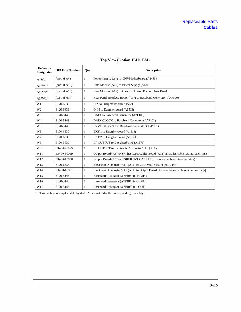
Replaceable PartsCables
Top View (Option 1EH/1EM)
Reference Designator
HP Part Number Qty Description
A4W11
1. This cable is not replaceable by itself. You must order the corresponding assembly.
(part of A4) 1 Power Supply (A4) to CPU/Motherboard (A14J6)
A16W11 (part of A16) 1 Line Module (A16) to Power Supply (A4J1)
A16W21 (part of A16) 1 Line Module (A16) to Chassis Ground Post on Rear Panel
A17W11 (part of A17) 1 Rear Panel Interface Board (A17) to Baseband Generator (A7P300)
W1 8120-6839 1 I IN to Daughterboard (A15J2)
W2 8120-6839 1 Q IN to Daughterboard (A15J3)
W3 8120-5143 1 DATA to Baseband Generator (A7P100)
W4 8120-5143 1 DATA CLOCK to Baseband Generator (A7P103)
W5 8120-5143 1 SYMBOL SYNC to Baseband Generator (A7P101)
W6 8120-6839 1 EXT 1 to Daughterboard (A15J4)
W7 8120-6839 1 EXT 2 to Daughterboard (A15J5)
W8 8120-6839 1 LF OUTPUT to Daughterboard (A15J6)
W9 E4400-20025 1 RF OUTPUT to Electronic Attenuator/RPP (AT1)
W11 E4400-60059 1 Output Board (A9) to Synthesizer/Doubler Board (A12) (includes cable retainer and ring)
W12 E4400-60060 1 Output Board (A9) to COHERENT CARRIER (includes cable retainer and ring)
W13 8120-6837 1 Electronic Attenuator/RPP (AT1) to CPU/Motherboard (A14J14)
W14 E4400-60061 1 Electronic Attenuator/RPP (AT1) to Output Board (A9) (includes cable retainer and ring)
W15 8120-5143 1 Baseband Generator (A7P403) to 13 MHz
W16 8120-5143 1 Baseband Generator (A7P404) to Q OUT
W17 8120-5143 1 Baseband Generator (A7P405) to I OUT
3-25

Replaceable PartsCables
Top View (Option 1EH/1EM)
3-26

Replaceable PartsCables
Top View (Options UN3/1EM & UN4/1EM)
Reference Designator
HP Part Number Qty Description
A4W11
1. This cable is not replaceable by itself. You must order the corresponding assembly.
(part of A4) 1 Power Supply (A4) to CPU/Motherboard (A14J6)
A16W11 (part of A16) 1 Line Module (A16) to Power Supply (A4J1)
A16W21 (part of A16) 1 Line Module (A16) to Chassis Ground Post on Rear Panel
A17W11 (part of A17) 1 Rear Panel Interface Board (A17) to Data Generator (A8P2)
W1 8120-6839 1 I IN to Daughterboard (A15J2)
W2 8120-6839 1 Q IN to Daughterboard (A15J3)
W3 8120-5143 1 DATA to Data Generator (A8J2)
W4 8120-5143 1 DATA CLOCK to Data Generator (A8J1)
W5 8120-5143 1 SYMBOL SYNC to Data Generator (A8J3)
W6 8120-6839 1 EXT 1 to Daughterboard (A15J4)
W7 8120-6839 1 EXT 2 to Daughterboard (A15J5)
W8 8120-6839 1 LF OUTPUT to Daughterboard (A15J6)
W9 E4400-20025 1 RF OUTPUT to Electronic Attenuator/RPP (AT1)
W11 E4400-60059 1 Output Board (A9) to Synthesizer/Doubler Board (A12) (includes cable retainer and ring)
W12 E4400-60060 1 Output Board (A9) to COHERENT CARRIER (includes cable retainer and ring)
W13 8120-6837 1 Electronic Attenuator/RPP (AT1) to CPU/Motherboard (A14J14)
W14 E4400-60061 1 Electronic Attenuator/RPP (AT1) to Output Board (A9) (includes cable retainer and ring)
W15 8120-5143 1 Baseband Generator (A7P403) to 13 MHz
W16 8120-5143 1 Baseband Generator (A7P404) to Q OUT
W17 8120-5143 1 Baseband Generator (A7P405) to I OUT
W19 8120-8349 1 Baseband Generator (A7P300) to Data Generator (A8P3)
3-27

Replaceable PartsCables
Top View (Options UN3/1EM & UN4/1EM)
3-28

Replaceable PartsCables
NOTE: W1 through W9 are not present on the front panel with Option 1EM.
Inside Front Panel View
Reference Designator
HP Part Number Qty Description
A1W11
1. This cable is not replaceable by itself. You must order the corresponding assembly.
(part of A1) 1 Front Panel Board (A1) to CPU/Motherboard (A14J20)
A2DS1W11 (part of A2DS1) 1 Florescent Lamp (A2DS1) to A3W2
A3W11 (part of A3) 1 Inverter (A3) to CPU/Motherboard (A14J19)
A3W21 (part of A3) 1 Inverter (A3) to A2DS1W1
B1W11 (part of B1) 1 Small Fan (B1) to CPU/Motherboard (A14J16)
B2W11 (part of B2) 1 Large Fan (B2) to CPU/Motherboard (A14J17)
W1 8120-6758 1 I IN to Daughterboard (A15J2)
W2 8120-6758 1 Q IN to Daughterboard (A15J3)
W3 8120-5401 1 DATA to Baseband Generator (A7P100) (Options 1EH, UN3, UN4)
W4 8120-5401 1 DATA CLOCK to Baseband Generator (A7P103) (Options 1EH, UN3, UN4)
W5 8120-5401 1 SYMBOL SYNC to Baseband Generator (A7P101) (Options 1EH, UN3, UN4)
W6 8120-6758 1 EXT 1 to Daughterboard (A15J4)
W7 8120-6758 1 EXT 2 to Daughterboard (A15J5)
W8 8120-6758 1 LF OUTPUT to Daughterboard (A15J6)
W9 E4400-20018 1 RF OUTPUT to Electronic Attenuator/RPP (AT1)
W10 8120-6759 1 Display (A2) to CPU/Motherboard (A14J21)
3-29

Replaceable PartsCables
Inside Front Panel View
NOTE: The figure above represents an Option 1EH, UN3, or UN4 front panel assembly. On a standard model, W3, W4, and W5 do not exist and the front panel connectors for W1 and W2 will be in a slightly different location.
3-30

Replaceable PartsCables
Attenuator View
Reference Designator
HP Part Number Qty Description
W1 8120-6758 1 I IN to Daughterboard (A15J2)
W2 8120-6758 1 Q IN to Daughterboard (A15J3)
W6 8120-6758 1 EXT 1 to Daughterboard (A15J4)
W7 8120-6758 1 EXT 2 to Daughterboard (A15J5)
W8 8120-6758 1 LF OUTPUT to Daughterboard (A15J6)
W9 E4400-20018 1 RF OUTPUT to Electronic Attenuator/RPP (AT1)
W11 E4400-60059 1 Output Board (A9) to Synthesizer/Doubler Board (A12) (includes cable retainer and ring)
W12 E4400-60060 1 Output Board (A9) to COHERENT CARRIER (includes cable retainer and ring)
W13 8120-6837 1 Electronic Attenuator/RPP (AT1) to CPU/Motherboard (A14J14)
W14 E4400-60061 1 Electronic Attenuator/RPP (AT1) to Output Board (A9) (includes cable retainer and ring)
3-31

Replaceable PartsCables
Attenuator View
3-32

Replaceable PartsCables
Attenuator View (Option 1EM)
Reference Designator
HP Part Number Qty Description
W1 8120-6839 1 I IN to Daughterboard (A15J2)
W2 8120-6839 1 Q IN to Daughterboard (A15J3)
W6 8120-6839 1 EXT 1 to Daughterboard (A15J4)
W7 8120-6839 1 EXT 2 to Daughterboard (A15J5)
W8 8120-6839 1 LF OUTPUT to Daughterboard (A15J6)
W9 E4400-20025 1 RF OUTPUT to Electronic Attenuator/RPP (AT1)
W11 E4400-60059 1 Output Board (A9) to Synthesizer/Doubler Board (A12) (includes cable retainer and ring)
W12 E4400-60060 1 Output Board (A9) to COHERENT CARRIER (includes cable retainer and ring)
W13 8120-6837 1 Electronic Attenuator/RPP (AT1) to CPU/Motherboard (A14J14)
W14 E4400-60061 1 Electronic Attenuator/RPP (AT1) to Output Board (A9) (includes cable retainer and ring)
3-33

Replaceable PartsCables
Attenuator View (Option 1EM)
3-34

Replaceable PartsHardware and Other Instrument Parts
Hardware and Other Instrument Parts
Top View
Item No. HP Part Number Qty Description
1 1400-0054 1 Clamp-Semi-Rigid Cable (W14)
2 0515-0372 1 Screw-Machine M3x8 CW-PN-TX
3 0515-0430 2 Screw-Machine M3x6 CW-PN-TX
4 1400-1594 1 Clamp-Flexible Cables (not used on Option 1EM)
5 0361-1341 4 Rivet-Plastic
6 0515-0374 4 Screw-Machine M3x10 CW-PN-TX
8 0400-0001 1 Grommet Round .562ID (not used on Option 1EM)
9 4320-0402 1 Channel NPR .062W (Options 1EH, UN3, UN4)
10 0400-0001 1 Grommet Round .562ID (Options 1EH/1EM, UN3/1EM, UN4/1EM)
11 0400-0001 1 Grommet Round .562ID (Option 1EM)
3-35

Replaceable PartsHardware and Other Instrument Parts
Top View
3-36
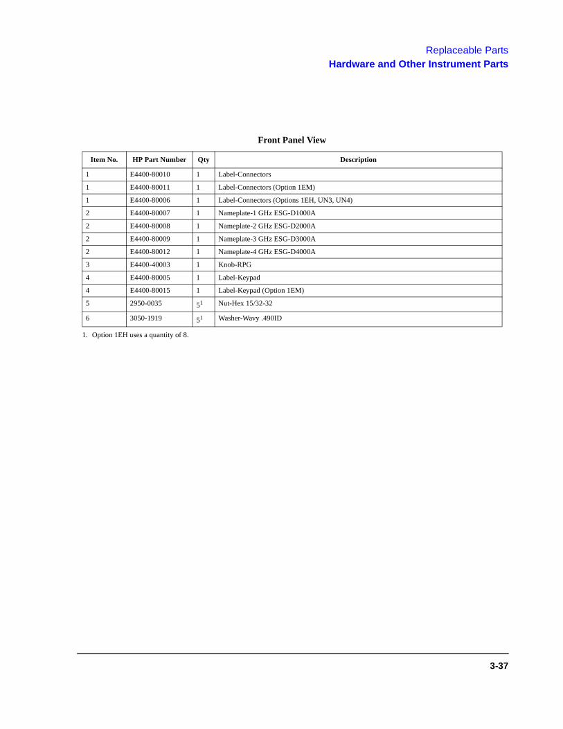
Replaceable PartsHardware and Other Instrument Parts
Front Panel View
Item No. HP Part Number Qty Description
1 E4400-80010 1 Label-Connectors
1 E4400-80011 1 Label-Connectors (Option 1EM)
1 E4400-80006 1 Label-Connectors (Options 1EH, UN3, UN4)
2 E4400-80007 1 Nameplate-1 GHz ESG-D1000A
2 E4400-80008 1 Nameplate-2 GHz ESG-D2000A
2 E4400-80009 1 Nameplate-3 GHz ESG-D3000A
2 E4400-80012 1 Nameplate-4 GHz ESG-D4000A
3 E4400-40003 1 Knob-RPG
4 E4400-80005 1 Label-Keypad
4 E4400-80015 1 Label-Keypad (Option 1EM)
5 2950-0035 51
1. Option 1EH uses a quantity of 8.
Nut-Hex 15/32-32
6 3050-1919 51 Washer-Wavy .490ID
3-37

Replaceable PartsHardware and Other Instrument Parts
Front Panel View
3-38
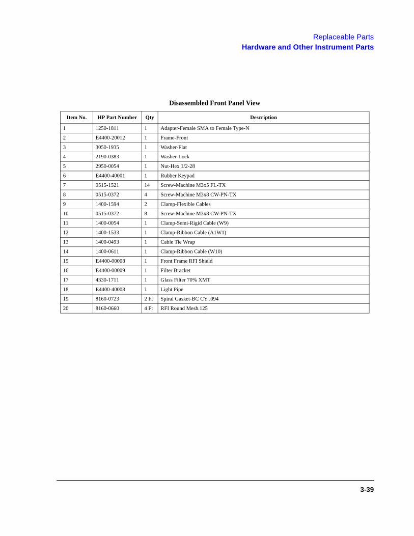
Replaceable PartsHardware and Other Instrument Parts
Disassembled Front Panel View
Item No. HP Part Number Qty Description
1 1250-1811 1 Adapter-Female SMA to Female Type-N
2 E4400-20012 1 Frame-Front
3 3050-1935 1 Washer-Flat
4 2190-0383 1 Washer-Lock
5 2950-0054 1 Nut-Hex 1/2-28
6 E4400-40001 1 Rubber Keypad
7 0515-1521 14 Screw-Machine M3x5 FL-TX
8 0515-0372 4 Screw-Machine M3x8 CW-PN-TX
9 1400-1594 2 Clamp-Flexible Cables
10 0515-0372 8 Screw-Machine M3x8 CW-PN-TX
11 1400-0054 1 Clamp-Semi-Rigid Cable (W9)
12 1400-1533 1 Clamp-Ribbon Cable (A1W1)
13 1400-0493 1 Cable Tie Wrap
14 1400-0611 1 Clamp-Ribbon Cable (W10)
15 E4400-00008 1 Front Frame RFI Shield
16 E4400-00009 1 Filter Bracket
17 4330-1711 1 Glass Filter 70% XMT
18 E4400-40008 1 Light Pipe
19 8160-0723 2 Ft Spiral Gasket-BC CY .094
20 8160-0660 4 Ft RFI Round Mesh.125
3-39
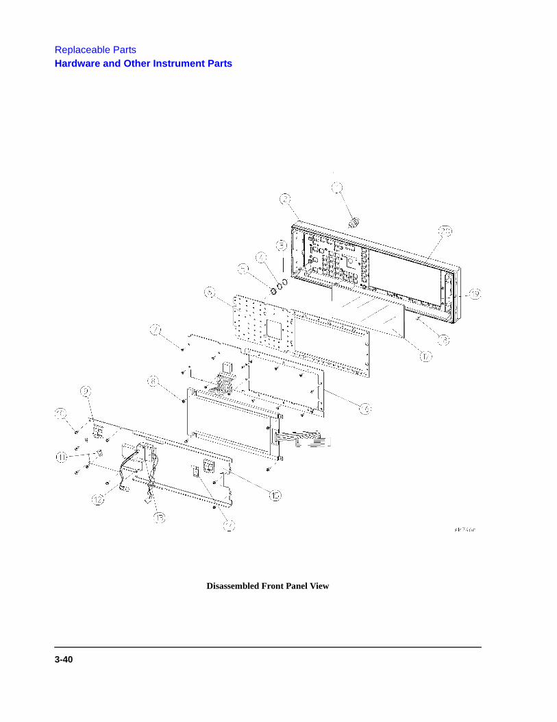
Replaceable PartsHardware and Other Instrument Parts
Disassembled Front Panel View
3-40
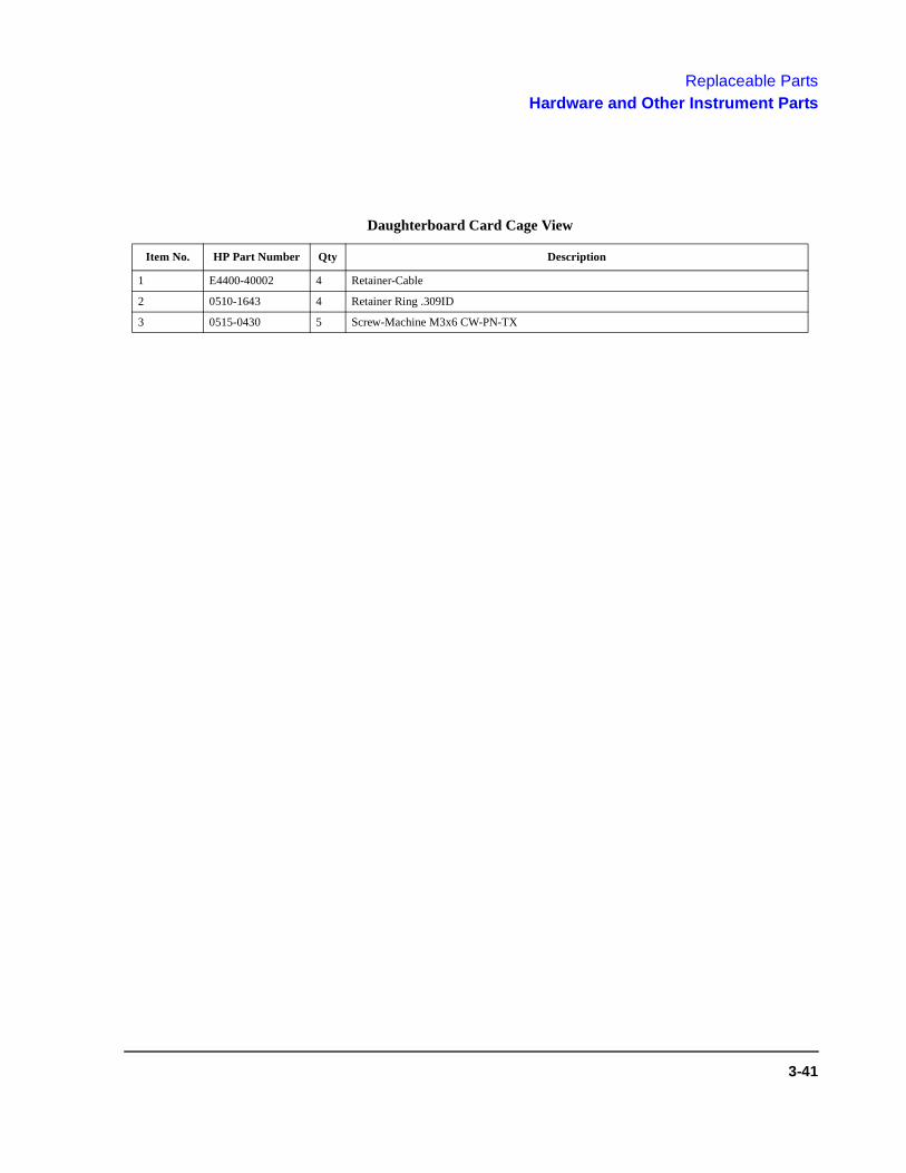
Replaceable PartsHardware and Other Instrument Parts
Daughterboard Card Cage View
Item No. HP Part Number Qty Description
1 E4400-40002 4 Retainer-Cable
2 0510-1643 4 Retainer Ring .309ID
3 0515-0430 5 Screw-Machine M3x6 CW-PN-TX
3-41

Replaceable PartsHardware and Other Instrument Parts
Daughterboard Card Cage View
3-42

Replaceable PartsHardware and Other Instrument Parts
Rear Panel View
Item No. HP Part Number Qty Description
1 0515-0372 10 Screw-Machine M3x8 CW-PN-TX
2 E4400-00002 1 Panel-Rear
2 E4400-00016 1 Panel-Rear (Options 1EH, UN3, UN4)
3 0515-0372 1 Screw-Machine M3x8 CW-PN-TX (used to attach item 4))
4 1250-2759 1 Dust Cap Female SMA
5 1250-1753 1 Adapter-Female SMA to Female SMA
7 E4400-00017 1 Serial Number Plate
8 0515-1102 2 Screw-Machine M3x8 FL-TX
9 0380-0644 2 Standoff-Hex .327L 6-32
10 2190-0577 2 Washer-Lock
11 0380-2079 2 Standoff-Hex .312L 4-40
12 2190-0003 2 Washer-Lock
13 6960-0002 3 Plug-Hole .500D (Options 1EH, UN3, UN4)
14 2950-0054 5 Nut-Hex 1/2-28
15 2190-0068 5 Washer-Lock .505ID
16 2950-0035 11 Nut-Hex 15/32-32 (Options 1EH, UN3, UN4)
17 2190-0102 11 Washer-Lock .472ID (Options 1EH, UN3, UN4)
3-43

Replaceable PartsHardware and Other Instrument Parts
Rear Panel View
3-44

Replaceable PartsHardware and Other Instrument Parts
Rear Panel View (Option 1EM)
Item No. HP Part Number Qty Description
1 0515-0372 10 Screw-Machine M3x8 CW-PN-TX
2 E4400-00010 1 Panel-Rear
3 0515-0372 1 Screw-Machine M3x8 CW-PN-TX (used to attach item 4)
4 1250-2759 1 Dust Cap Female SMA
5 1250-1753 1 Adapter-Female SMA to Female SMA
7 2950-0035 5 Nut-Hex 15/32-32
8 2190-0102 5 Washer-Lock .472ID
9 08559-60002 1 RF Output Assy
10 2950-0132 1 Nut-Hex 7/16-28
11 2190-0102 1 Washer-Lock
13 E4400-00017 1 Serial Number Plate
14 0515-1102 2 Screw-Machine M3x8 FL-TX
15 0380-0644 2 Standoff-Hex .327L 6-32
16 2190-0577 2 Washer-Lock
17 0380-2079 2 Standoff-Hex .312L 4-40
18 2190-0003 2 Washer-Lock
19 2950-0054 5 Nut-Hex 1/2-28
20 2190-0068 5 Washer-Lock .505ID
21 E4400-00018 1 Panel-Rear (Options 1EH, UN3, UN4)
22 2950-0078 14 Nut-Hex 10-32 (for the SMBs) (Options 1EH, UN3, UN4)
23 2190-0124 14 Washer-Lock .195ID (for the SMBs) (Options 1EH, UN3, UN4)
3-45

Replaceable PartsHardware and Other Instrument Parts
Rear Panel View (Option 1EM)
3-46
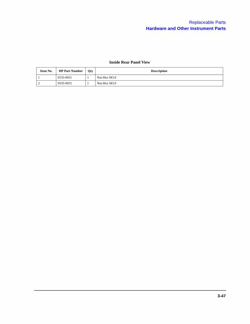
Replaceable PartsHardware and Other Instrument Parts
Inside Rear Panel View
Item No. HP Part Number Qty Description
1 0535-0031 1 Nut-Hex M3.0
2 0535-0031 1 Nut-Hex M3.0
3-47

Replaceable PartsHardware and Other Instrument Parts
Inside Rear Panel View
3-48

Replaceable PartsHardware and Other Instrument Parts
Instrument Chassis with Top and Right-Side Hardware
Item No. HP Part Number Qty Description
1 0515-1269 2 Screw-Machine M4X10 FL-TX
2 0515-2087 4 Screw-Machine M3x6 CW-BN-TX
3 E4400-00003 1 Cover-Side
4 E4400-00001 1 Chassis
5 E4400-00006 1 Cover-Top Chassis
6 0515-0430 11 Screw-Machine M3x6 CW-PN-TX
7 E4400-80018 1 Label-Connection Diagram (Option 1EH only)
7 E4400-80046 1 Label-Connection Diagram
3-49
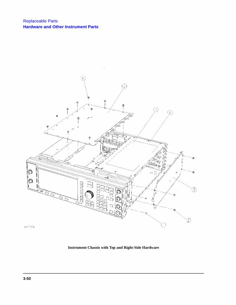
Replaceable PartsHardware and Other Instrument Parts
Instrument Chassis with Top and Right-Side Hardware
3-50
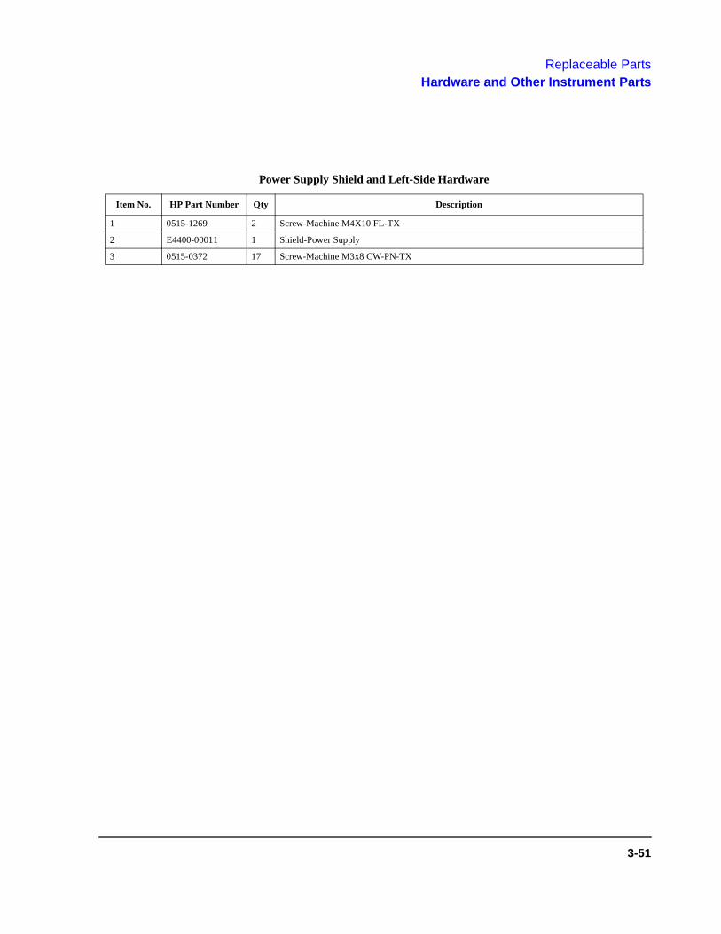
Replaceable PartsHardware and Other Instrument Parts
Power Supply Shield and Left-Side Hardware
Item No. HP Part Number Qty Description
1 0515-1269 2 Screw-Machine M4X10 FL-TX
2 E4400-00011 1 Shield-Power Supply
3 0515-0372 17 Screw-Machine M3x8 CW-PN-TX
3-51
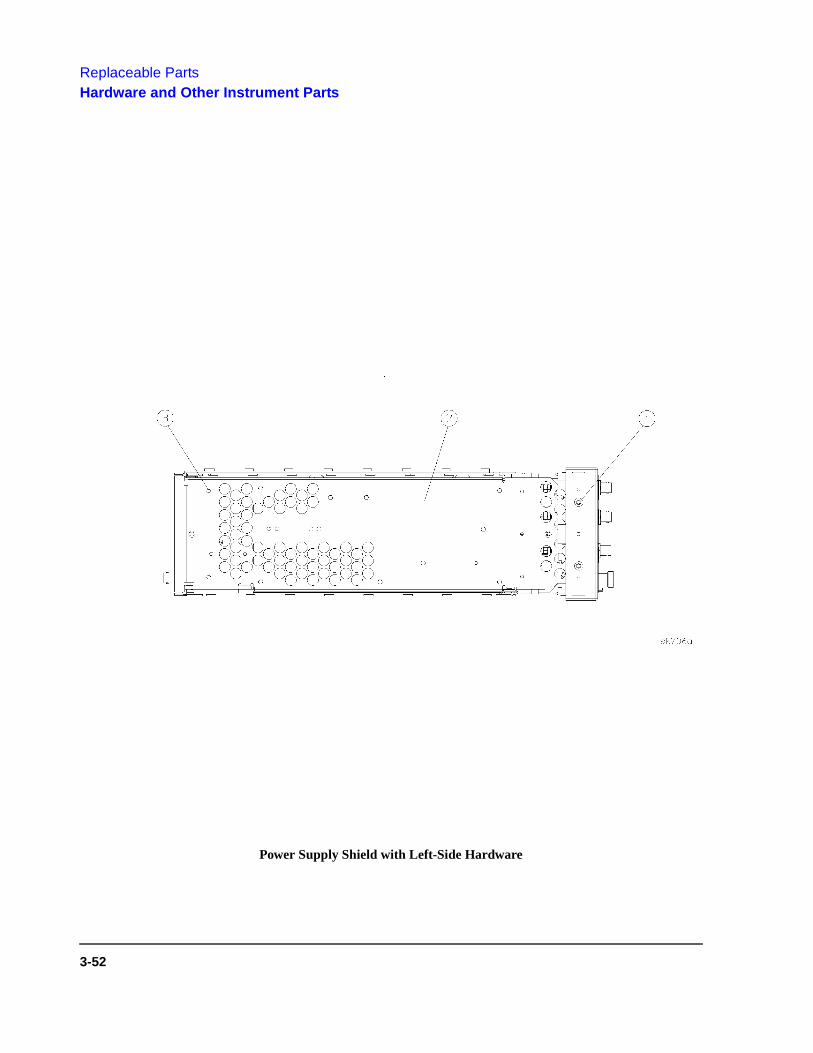
Replaceable PartsHardware and Other Instrument Parts
Power Supply Shield with Left-Side Hardware
3-52
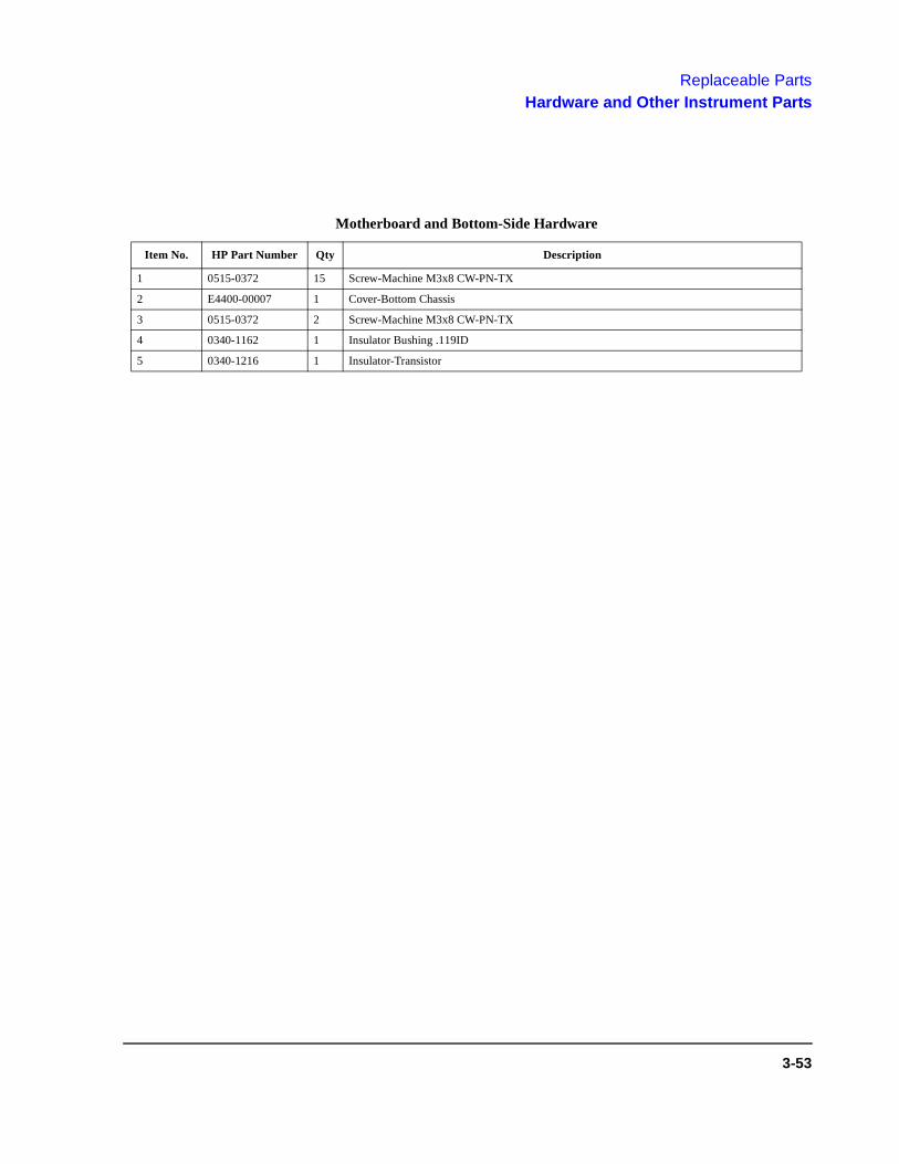
Replaceable PartsHardware and Other Instrument Parts
Motherboard and Bottom-Side Hardware
Item No. HP Part Number Qty Description
1 0515-0372 15 Screw-Machine M3x8 CW-PN-TX
2 E4400-00007 1 Cover-Bottom Chassis
3 0515-0372 2 Screw-Machine M3x8 CW-PN-TX
4 0340-1162 1 Insulator Bushing .119ID
5 0340-1216 1 Insulator-Transistor
3-53

Replaceable PartsHardware and Other Instrument Parts
Motherboard and Bottom-Side Hardware
3-54

Replaceable PartsHardware and Other Instrument Parts
Instrument Cover and Associated Parts
Item No. HP Part Number Qty Description
1 0515-1619 4 Screw-Machine M4x25 PN-TX
2 5182-1275 4 Foot-Rear Long
3 5041-8801 4 Feet-Bottom
4 1460-1345 2 Spring-Wire Frame 3.000 Long
5 5041-9171 2 Side Trim
6 E4400-60026 2 Assy-Strap Handle
7 E4400-00004 1 Cover-Instrument
3-55
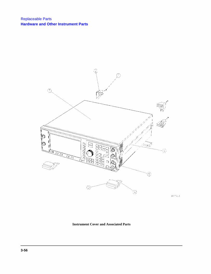
Replaceable PartsHardware and Other Instrument Parts
Instrument Cover and Associated Parts
3-56

Replaceable PartsMiscellaneous
Miscellaneous
Accessories
Description HP Part Number
Connector End Cap-RF Output 1401-0247
Connector End Cap-HP-IB 1401-5007
Connector End Cap-Aux Out 1252-4696
HP-IB Cable, 1M (3.3 Ft) HP 10833A
HP-IB Cable, 2M (6.6 Ft) HP 10833B
HP-IB Cable, 4M (13.2 Ft) HP 10833C
HP-IB Cable, 0.5M (1.6 Ft) HP 10833D
Remote Interface HP 83300A
Transit Case 9211-1296
Documentation
Description HP Part Number
HP ESG Series Signal Generators Manual Set (includes the four manuals listed below) E4400-90075
HP ESG Series Signal Generators User’s Guide E4400-90076
HP ESG Series Signal Generators Programming Guide E4400-90077
HP ESG Series Signal Generators Quick Reference Guide E4400-90078
HP ESG Series Signal Generators Calibration Guide E4400-90079
HP ESG Series Signal Generators Service Guide E4400-90008
HP ESG-D Series Signal Generators Manual Set (includes the four manuals listed below) E4400-90080
HP ESG-D Series Signal Generators User’s Guide E4400-90081
HP ESG-D Series Signal Generators Programming Guide E4400-90082
HP ESG-D Series Signal Generators Quick Reference Guide E4400-90083
HP ESG-D Series Signal Generators Calibration Guide E4400-90084
HP ESG-D Series Signal Generators Service Guide E4400-90014
HP ESG Series and HP ESG-D Series Signal Generators Component-Level Information E4400-90015
HP ESG Series Signal Generators User’s Guide - Chinese E4400-90022
HP ESG Series Signal Generators User’s Guide - Korean E4400-90023
HP ESG Series Signal Generators User’s Guide - Taiwanese E4400-90024
HP ESG Series Signal Generators User’s Guide - Japanese E4400-90025
HP ESG Series Signal Generators User’s Guide - Spanish E4400-90026
HP ESG Series Signal Generators User’s Guide - German E4400-90027
HP ESG-D Series Signal Generators User’s Guide - Chinese E4400-90028
3-57

Replaceable PartsMiscellaneous
HP ESG-D Series Signal Generators User’s Guide - Korean E4400-90029
HP ESG-D Series Signal Generators User’s Guide - Taiwanese E4400-90030
HP ESG-D Series Signal Generators User’s Guide - Japanese E4400-90031
HP ESG-D Series Signal Generators User’s Guide - Spanish E4400-90032
HP ESG-D Series Signal Generators User’s Guide - German E4400-90033
ESD Supplies
Description HP Part Number
2 X 4 Ft Antistatic Table Mat with 15 Ft Ground Wire 9300-0797
5 Ft Grounding Cord (for wrist strap) 9300-0980
Adjustable Antistatic Wrist Strap 9300-1367
Antistatic Heel Strap (for use on conductive floors) 9300-1126
Kits
Description HP Part Number
Kit-Firmware Upgrade (RS-232 cable not included - must order separately) E4400-60046
Kit-Firmware Upgrade with ESG Series Manual Set (RS-232 cable not included - must order separately) E4400-60054
Kit-Firmware Upgrade with ESG-D Series Manual Set (RS-232 cable not included - must order separately) E4400-60055
Kit-RS-232 Cable E4400-60049
Kit-Rack Mount Flanges without Handles (Option 1CM) 5063-9214
Kit-Rack Mount Flanges with Handles (Option 1CP) 5063-9221
Retrofit Kit-Converts Analog Models (ESG Series) to Digital (ESG-D Series) E4400-60047
Retrofit Kit-High Stability Timebase (conversion to Option 1E5) E4400-60032
Documentation
Description HP Part Number
3-58

4 Assembly Replacement
This chapter provides removal and replacement procedures for the major assemblies of your signal generator.
4-1

Assembly ReplacementBefore You Replace an Assembly
Before You Replace an Assembly
Avoid Personal Injury
WARNING: These servicing instructions are for use by qualified personal only. To avoid electrical shock, do not perform any servicing unless you are qualified to do so.
WARNING: The opening of covers or removal of parts is likely to expose dangerous voltages. Disconnect the product from all voltage sources while it is being opened.
WARNING: The detachable power cord is the instrument disconnecting device. It disconnects the mains circuits from the mains supply before other parts of the instrument. The front panel switch is only a standby switch and is not a LINE switch.
WARNING: The power cord is connected to internal capacitors that may remain live for 5 seconds after disconnecting the plug from its power supply.
Prevent ESD Damage
CAUTION: Many of the assemblies in this instrument are very susceptible to damage from ESD (electrostatic discharge). Perform service procedures only at a static-safe workstation and wear a grounding strap.
4-2
Assembly ReplacementAssemblies That You Can Replace
Assemblies That You Can Replace
This chapter provides removal and replacement procedures for the following assemblies:
• Instrument Cover• Front Panel• Front Panel (Option 1EM)• Rear Panel• Rear Panel (Option 1EM)• A1 Front Panel Board• A2 Display• A2DS1 Fluorescent Lamp• A3 Inverter• A4 Power Supply• A4 Power Supply (Option 1EM)• A7 Baseband Generator Board (Option 1EH)• A7 Baseband Generator Board (Options UN3 & UN4)• A8 Data Generator Board (Options UN3 & UN4) • A9, A11, and A12 Daughterboard Card Cage Boards• A14 CPU/Motherboard• A14BT1 Battery• A15 Daughterboard• A16 Line Module• A17 Rear Panel Interface Board (Options 1EH, UN3, UN4)• AT1 Electronic Attenuator/RPP• B1 Small Fan Assembly• B2 Large Fan Assembly• W11, W12, and W14 Semi-Rigid Cables
After Replacing an Assembly
After you have replaced or repaired an assembly, certain performance tests and adjustments may have to be performed. Chapter 5, "Post-Repair Procedures," lists the performance tests and adjustments required for each assembly.
4-3

Assembly ReplacementInstrument Cover
Instrument Cover
Tools Required• T-15 TORX screwdriver• T-20 TORX screwdriver
Removal1. Remove the two strap handles (item 1) from each side of the signal generator by loosening the two screws
(item 2) on each handle.
2. Remove the four bottom feet (item 3).
3. Remove the four rear feet (item 4) from the signal generator by removing the four screws (item 5) that secure them.
4. Slide the instrument cover (item 6) off the back of the signal generator.
Replacement1. Reverse the removal procedure and do the following:
• Torque the rear feet screws (item 4) to 21 in-lbs.
• Torque the strap handle screws (item 2) to 21 in-lbs.
4-4

Assembly ReplacementInstrument Cover
Instrument Cover
4-5
Assembly ReplacementFront Panel
Front Panel
Tools Required• T-10 TORX screwdriver• T-15 TORX screwdriver• 5/16-inch open-end wrench• long nose pliers (used for disconnecting wires from the daughterboard)
Removal1. Remove the instrument cover. (Refer to "Instrument Cover" in this chapter.)
2. Remove the top cover by removing the 11 screws that secure it.
3. Disconnect A1W1, A3W1, and W10 from the motherboard (A14). To disconnect W10 you must first unlock the motherboard connector by pulling out the locking mechanism (much like pulling out a drawer).
4. Disconnect W1, W2, W6, W7, and W8 from the daughterboard (A15).
5. If you have Option UN3 or UN4, disconnect W3, W4, and W5 from the data generator board (A8).
If you have Option 1EH, disconnect W3, W4, and W5 from the baseband generator board (A7).
NOTE: The figure on the adjacent page represents an Option UN3 or UN4. Option 1EH is not shown.
6. Disconnect W9 from the electronic attenuator/RPP (AT1).
4-6
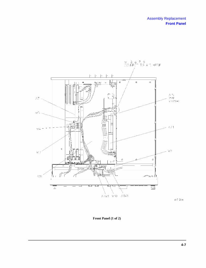
Assembly ReplacementFront Panel
Front Panel (1 of 2)
4-7
Assembly ReplacementFront Panel
7. Carefully peel off the side trim (item 1) from the sides of the front panel assembly (item 2).
8. Remove the four screws (item 3) that attach the front panel assembly to the instrument chassis.
9. Pull the front panel assembly away from the instrument chassis.
Replacement1. Reverse the removal procedure and do the following:
• Refer to Chapter 3, "Replaceable Parts," to verify that the cables are reconnected in the correct locations.
• To reconnect W10 to its motherboard connector do the following:
a Ensure the motherboard connector is unlocked by pulling out the locking mechanism (much like pulling out a drawer).
b Insert W10 into the connector making sure the conductive contacts are facing up (the blue insulation should be facing down).
c Lock the connector by pushing in on the locking mechanism.
NOTE: Intermittent display problems may result if W10 is not connected correctly.
• Torque W9 to 9 in-lbs.
• Torque all T-10 TORX screws to 9 in-lbs.
• Torque all T-15 TORX screws to 21 in-lbs.
4-8

Assembly ReplacementFront Panel
Front Panel (2 of 2)
4-9

Assembly ReplacementFront Panel (Option 1EM)
Front Panel (Option 1EM)
Tools Required• T-10 TORX screwdriver• T-15 TORX screwdriver
Removal1. Remove the instrument cover. (Refer to "Instrument Cover" in this chapter.)
2. Remove the top cover by removing the 11 screws that secure it.
3. Disconnect A1W1, A3W1, and W10 from the motherboard (A14). To disconnect W10 you must first unlock the motherboard connector by pulling out the locking mechanism (much like pulling out a drawer).
4-10

Assembly ReplacementFront Panel (Option 1EM)
Front Panel (Option 1EM) (1 of 2)
4-11
Assembly ReplacementFront Panel (Option 1EM)
4. Carefully peel of the side trim (item 1) from the sides of the front panel assembly (item 2).
5. Remove the four screws (item 3) that attach the front panel assembly to the instrument chassis.
6. Pull the front panel assembly away from the instrument chassis.
Replacement1. Reverse the removal procedure and do the following:
• Refer to Chapter 3, "Replaceable Parts," to verify that the cables are reconnected in the correct locations.
• To reconnect W10 to its motherboard connector do the following:
a Ensure the motherboard connector is unlocked by pulling out the locking mechanism (much like pulling out a drawer).
b Insert W10 into the connector making sure the conductive contacts are facing up (the blue insulation should be facing down).
c Lock the connector by pushing in on the locking mechanism.
NOTE: Intermittent display problems may result if W10 is not connected correctly.
• Torque all T-10 TORX screws to 9 in-lbs.
• Torque all T-15 TORX screws to 21 in-lbs.
4-12

Assembly ReplacementFront Panel (Option 1EM)
Front Panel (Option 1EM) (2 of 2)
4-13
Assembly ReplacementRear Panel
Rear Panel
Tools Required• T-10 TORX screwdriver• 3/16-inch wrench or nut driver• 9/32-inch wrench or nut driver• 5/16-inch open-end wrench• 5/8-inch wrench or nut driver• long nose pliers
Removal1. Remove the instrument cover. (Refer to "Instrument Cover" in this chapter.)
2. Remove the top cover by removing the 11 screws that secure it.
3. Remove the bottom cover by removing the 15 screws that secure it.
4. Disconnect A16W1 from the power supply (A4). A16W1 can be accessed through an opening on the bottom of the power supply shield (item 1).
5. If you have Option UN3 or UN4, disconnect A17W1 from the data generator board (A8). Disconnect W15, W16, and W17 from the baseband generator board (A7).
If you have Option 1EH, disconnect A17W1, W15, W16, and W17 from the baseband generator board (A7).
NOTE: The figure on the adjacent page represents an Option UN3 or UN4. Option 1EH is not shown.
6. Disconnect W12 from the adapter assembly on the rear panel.
4-14

Assembly ReplacementRear Panel
Rear Panel (1 of 2)
4-15

Assembly ReplacementRear Panel
7. Remove the nuts and washers securing the five BNC connectors (item 1) at the base of the rear panel.
8. Remove the hex screws and washers that secure the AUXILARY INTERFACE (item 2) and the HP-IB connector (item 3) to the rear panel.
9. Remove the 10 screws (item 4) that secure the rear panel to the instrument chassis. Do not remove the screw that secures the chain and cap for COHERENT CARRIER connector.
10. Pull the rear panel assembly away from the instrument chassis.
Replacement1. Reverse the removal procedure and do the following:
• Torque all T-10 TORX screws to 9 in-lbs.
• Torque the AUXILARY INTERFACE hex screws to 6 in-lbs.
• Torque the HP-IB hex screws to 9 in-lbs.
• Torque the five BNC connector nuts to 21 in-lbs.
• Torque W12 to 9 in-lbs.
• Refer to Chapter 3, "Replaceable Parts," to verify that the cables are reconnected in the correct locations.
4-16

Assembly ReplacementRear Panel
Rear Panel (2 of 2)
4-17

Assembly ReplacementRear Panel (Option 1EM)
Rear Panel (Option 1EM)
Tools Required• T-10 TORX screwdriver• 3/16-inch wrench or nut driver• 9/32-inch wrench or nut driver• 5/16-inch open-end wrench• 5/8-inch wrench or nut driver• long nose pliers
Removal1. Remove the instrument cover. (Refer to "Instrument Cover" in this chapter.)
2. Remove the top cover by removing the 11 screws that secure it.
3. Remove the bottom cover by removing the 15 screws that secure it.
4. Disconnect A16W1 from the power supply (A4). A16W1 can be accessed through an opening on the bottom of the power supply shield (item 1).
5. Disconnect W1, W2, W6, W7, and W8 from the daughterboard (A15).
6. If you have Option UN3 or UN4, disconnect A17W1,W3, W4, and W5 from the data generator board (A8). Disconnect W15, W16, and W17 from the baseband generator board (A7).
If you have Option 1EH, disconnect A17W1, W3, W4, W5, W15, W16, and W17 from the baseband generator board (A7).
NOTE: The figure on the adjacent page represents an Option UN3 or UN4. Option 1EH is not shown.
7. Disconnect W9 from the adapter assembly on the rear panel.
8. Disconnect W12 from the adapter assembly on the rear panel.
4-18

Assembly ReplacementRear Panel (Option 1EM)
Rear Panel (Option 1EM) (1 of 2)
4-19

Assembly ReplacementRear Panel (Option 1EM)
9. Remove the nuts and washers securing the five BNC connectors (item 1) at the base of the rear panel.
10. Remove the hex screws and washers that secure the AUXILARY INTERFACE (item 2) and the HP-IB connector (item 3) to the rear panel.
11. Remove the 10 screws (item 4) that secure the rear panel to the instrument chassis.
12. Pull the rear panel assembly away from the instrument chassis.
Replacement1. Reverse the removal procedure and do the following:
• Torque all T-10 TORX screws to 9 in-lbs.
• Torque the AUXILARY INTERFACE hex screws to 6 in-lbs.
• Torque the HP-IB hex screws to 9 in-lbs.
• Torque the five BNC connector nuts to 21 in-lbs.
• Torque W9 and W12 to 9 in-lbs.
• Refer to Chapter 3, "Replaceable Parts," to verify that the cables are reconnected in the correct locations.
4-20

Assembly ReplacementRear Panel (Option 1EM)
Rear Panel (Option 1EM) (2 of 2)
4-21
Assembly ReplacementA1 Front Panel Board
A1 Front Panel Board
Tools Required• T-10 TORX screwdriver• 5/16-inch open-end wrench
Removal1. Remove the front panel assembly. (Refer to "Front Panel" in this chapter.)
2. Remove the small bracket (item 1) that secures W9 (not shown) to the RFI shield (item 2). Disconnect W9.
3. Remove the RFI shield by removing the seven screws (item 3) that secure it.
4. Remove the display (A2) by removing the four screws (item 4) that secure it.
5. Remove the front panel knob (item 5) by pulling it directly away from the front panel.
6. Remove the front panel board (A1) by removing the nine screws (item 6) that secure it.
Replacement1. Reverse the removal procedure and do the following:
• Torque all T-10 TORX screws to 9 in-lbs.
• Torque W9 to 9 in-lbs.
4-22

Assembly ReplacementA1 Front Panel Board
A1 Front Panel Board
4-23

Assembly ReplacementA2 Display
A2 Display
Tools Required• T-10 TORX screwdriver• 5/16-inch open-end wrench
Removal1. Remove the front panel assembly. (Refer to "Front Panel" in this chapter.)
2. Remove the small bracket (item 1) that secures W9 (not shown) to the RFI shield (item 2). Disconnect W9.
3. Remove the RFI shield by removing the seven screws (item 3) that secure it.
4. Remove the display (A2) by removing the four screws (item 4) that secure it.
Replacement1. Reverse the removal procedure and do the following:
• Torque all T-10 TORX screws to 9 in-lbs.
• Torque W9 to 9 in-lbs.
4-24

Assembly ReplacementA2 Display
A2 Display
4-25

Assembly ReplacementA2DS1 Fluorescent Lamp
A2DS1 Fluorescent Lamp
Tools Required• Phillips #0 screwdriver
Removal1. Remove the display (A2). (Refer to "A2 Display" in this chapter.)
2. Loosen the screw (item 1) on the compartment door (item 2) of the display. Remove the door.
3. Remove the fluorescent lamp (A2DS1) from the compartment.
Replacement1. Reverse the removal procedure. Ensure the lamp is correctly positioned in the reflective paper of the compartment.
4-26
Assembly ReplacementA2DS1 Fluorescent Lamp
A2DS1 Fluorescent Lamp
4-27

Assembly ReplacementA3 Inverter
A3 Inverter
Tools Required• wire cutters
Removal
NOTE: It is best to attempt this procedure without removing the front panel assembly. If the front panel assembly is removed, you will be required to perform time-consuming “Power Level Accuracy” verification tests and adjustments.
1. Remove the instrument cover. (Refer to "Instrument Cover" in this chapter.)
2. Disconnect A3W2 from A2DS1W1.
3. Cut the tie wrap (item 1) that secures the inverter (A3) to the RFI shield (item 2).
4. Remove the inverter.
Replacement1. Reverse the removal procedure and secure the inverter (A3) with a new tie wrap.
4-28
Assembly ReplacementA3 Inverter
A3 Inverter
4-29

Assembly ReplacementA4 Power Supply
A4 Power Supply
Tools Required• T-10 TORX screwdriver• T-15 TORX screwdriver
Removal1. Remove the rear panel assembly. (Refer to "Rear Panel" in this chapter.)
2. Remove the screw (item 1) that attaches the motherboard (A14) to the bottom of the power supply shield(item 2).
NOTE: Before proceeding to the next step ensure that the instrument is fully supported on a flat surface. This will keep the front panel assembly stable during the time it is attached only to the right side of the instrument.
4-30

Assembly ReplacementA4 Power Supply
A4 Power Supply (1 of 2)
4-31

Assembly ReplacementA4 Power Supply
3. Disconnect A4W1 from the motherboard (A14).
4. Carefully peel off the side trim (item 3) from the left side of the front panel assembly (item 4).
5. Remove the two screws (item 5) that attach the power supply shield (item 2) to the front panel assembly.
6. Remove the five screws (item 6) that attach the power supply shield to the instrument chassis (item 7).
7. Lift the rear of the power supply shield one-quarter inch and then pull it away from the instrument chassis.
NOTE: While removing the power supply shield try to limit the movement of the front panel assembly. This will reduce the stress on W9.
8. Remove the 12 screws (item 8) that attach the power supply to the power supply shield.
9. Remove the power supply (A4) from the front end of the shield.
Replacement1. Reverse the removal procedure and do the following:
• Torque all T-10 TORX screws to 9 in-lbs.
• Torque all T-15 TORX screws to 21 in-lbs.
4-32
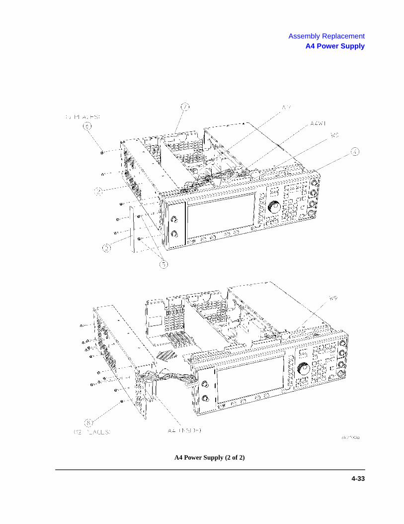
Assembly ReplacementA4 Power Supply
A4 Power Supply (2 of 2)
4-33
Assembly ReplacementA4 Power Supply (Option 1EM)
A4 Power Supply (Option 1EM)
Tools Required• T-10 TORX screwdriver
Removal1. Remove the front panel assembly. (Refer to "Front Panel (Option 1EM)" in this chapter.)
2. Remove the bottom cover by removing the 15 screws that secure it.
3. Remove the screw (item 1) that attaches the motherboard (A14) to the bottom of the power supply shield(item 2).
4. Disconnect A16W1 from the power supply (A4).
5. Remove the two screws (item 3) that attach the line module (A16) to the rear panel.
6. Remove the line module and A16W1 from the opening in the rear panel. The line module will remain connected to the rear panel, however, via the ground wire, A16W2. (Refer to the figure on page 37 of this chapter.)
7. Remove the three screws (item 4) that attach the rear panel to the power supply shield.
4-34
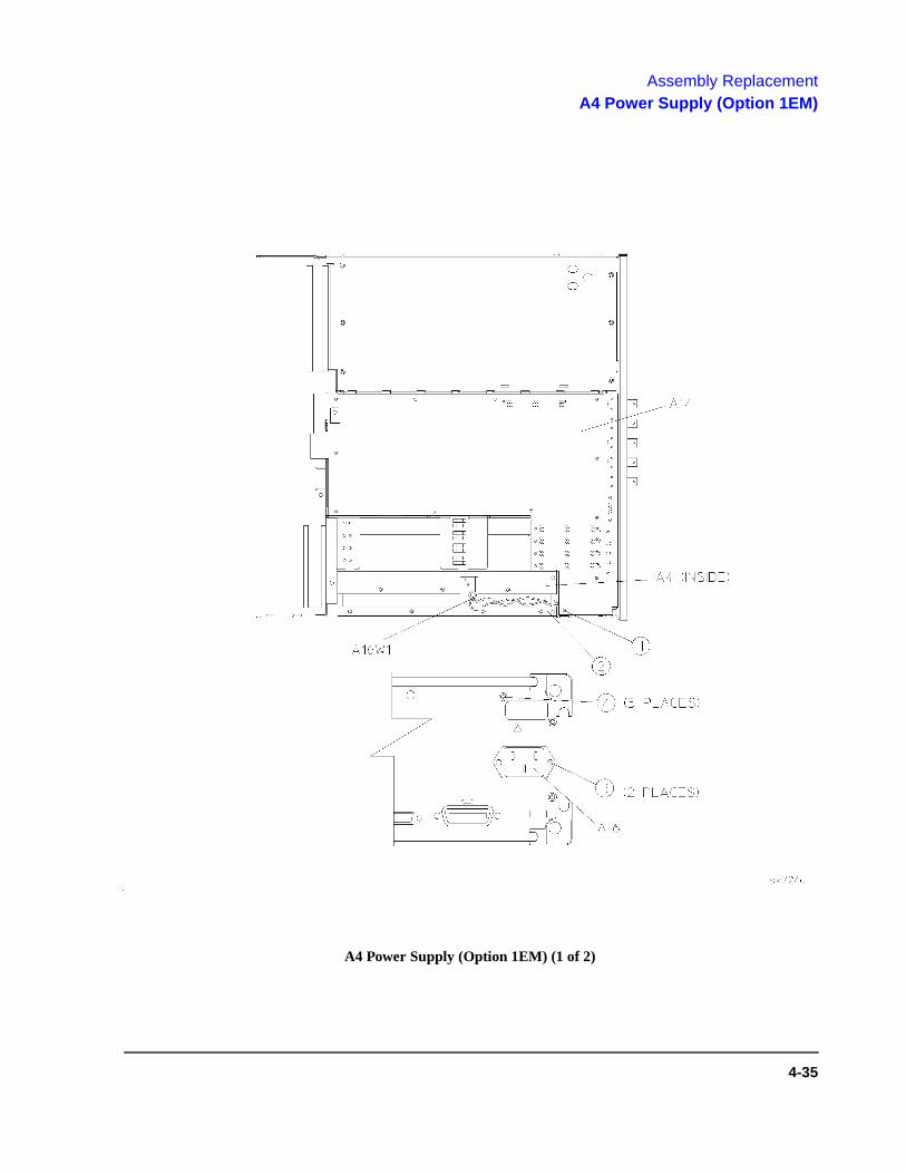
Assembly ReplacementA4 Power Supply (Option 1EM)
A4 Power Supply (Option 1EM) (1 of 2)
4-35

Assembly ReplacementA4 Power Supply (Option 1EM)
8. Disconnect A4W1 from the motherboard (A14).
9. Remove the five screws (item 5) that attach the power supply shield (item 2) to the instrument chassis (item 6).
10. Pull the power supply shield away from the instrument chassis.
11. Remove the 12 screws (item 7) that attach the power supply to the power supply shield.
12. Remove the power supply (A4) from the front end of the shield.
Replacement1. Reverse the removal procedure and torque all T-10 TORX screws to 9 in-lbs.
4-36

Assembly ReplacementA4 Power Supply (Option 1EM)
A4 Power Supply (Option 1EM) (2 of 2)
4-37

Assembly ReplacementA7 Baseband Generator Board (Option 1EH)
A7 Baseband Generator Board (Option 1EH)
Tools Required• T-10 TORX screwdriver• long nose pliers
Removal1. Remove the instrument cover. (Refer to "Instrument Cover" in this chapter.)
2. Remove the top cover by removing the 11 screws that secure it.
3. Disconnect W3, W4, W5, W15, W16, W17, and A17W1 from the baseband generator board (A7).
4. Pull up on the baseband generator board to remove it from the motherboard connector.
Replacement1. Reverse the removal procedure and do the following:
• Refer to Chapter 3, "Replaceable Parts," to verify that the cables are reconnected in the correct locations.
• Torque all T-10 TORX screws to 9 in-lbs.
4-38

Assembly ReplacementA7 Baseband Generator Board (Option 1EH)
A7 Baseband Generator Board (Option 1EH)
4-39

Assembly ReplacementA7 Baseband Generator Board (Options UN3 & UN4)
A7 Baseband Generator Board (Options UN3 & UN4)
Tools Required• T-10 TORX screwdriver• long nose pliers
Removal1. Remove the instrument cover. (Refer to "Instrument Cover" in this chapter.)
2. Remove the top cover by removing the 11 screws that secure it.
3. Disconnect W15, W16, W17, and W19 from the baseband generator board (A7)..
4. Pull up on the baseband generator board to remove it from the motherboard connector.
Replacement1. Reverse the removal procedure and do the following:
• Refer to Chapter 3, "Replaceable Parts," to verify that the cables are reconnected in the correct locations.
• Torque all T-10 TORX screws to 9 in-lbs.
4-40

Assembly ReplacementA7 Baseband Generator Board (Options UN3 & UN4)
A7 Baseband Generator Board (Options UN3 & UN4)
4-41

Assembly ReplacementA8 Data Generator Board (Options UN3 & UN4)
A8 Data Generator Board (Options UN3 & UN4)
Tools Required• T-10 TORX screwdriver• long nose pliers
Removal1. Remove the instrument cover. (Refer to "Instrument Cover" in this chapter.)
2. Remove the top cover by removing the 11 screws that secure it.
3. Disconnect A17W1,W3, W4, W5 , and W19 from the data generator board (A8).
4. Pull up on the data generator board to remove it from the motherboard connector.
Replacement1. Reverse the removal procedure and do the following:
• Refer to Chapter 3, "Replaceable Parts," to verify that the cables are reconnected in the correct locations.
• Torque all T-10 TORX screws to 9 in-lbs.
4-42
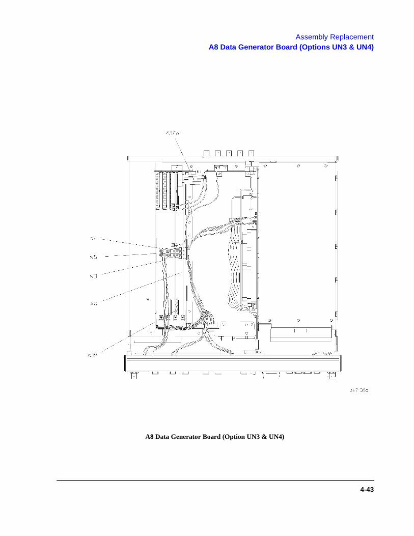
Assembly ReplacementA8 Data Generator Board (Options UN3 & UN4)
A8 Data Generator Board (Option UN3 & UN4)
4-43

Assembly ReplacementA9, A11, and A12 Daughterboard Card Cage Boards
A9, A11, and A12 Daughterboard Card Cage Boards
Use this procedure to remove any one of the following assemblies:
• Output Board (A9)• Reference Board (A11)• Synthesizer/Doubler Board (A12)
Tools Required• T-8 TORX screwdriver
Removal1. Remove the instrument cover. (Refer to "Instrument Cover" in this chapter.)
2. Remove the right-side cover by removing the four screws that attach it to the instrument chassis.
3. Simultaneously lift the left and right extractors (item 1) on the board you want to remove.
4. Remove the board from the card cage slot.
Replacement1. Reverse the removal procedure and torque all T-8 TORX screws to 9 in-lbs.
4-44

Assembly ReplacementA9, A11, and A12 Daughterboard Card Cage Boards
A9, A11, and A12 Daughterboard Card Cage Boards
4-45
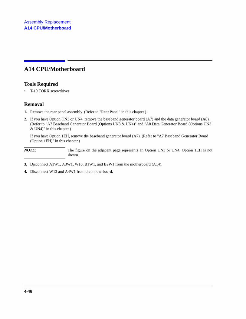
Assembly ReplacementA14 CPU/Motherboard
A14 CPU/Motherboard
Tools Required• T-10 TORX screwdriver
Removal1. Remove the rear panel assembly. (Refer to "Rear Panel" in this chapter.)
2. If you have Option UN3 or UN4, remove the baseband generator board (A7) and the data generator board (A8). (Refer to "A7 Baseband Generator Board (Options UN3 & UN4)" and "A8 Data Generator Board (Options UN3 & UN4)" in this chapter.)
If you have Option 1EH, remove the baseband generator board (A7). (Refer to "A7 Baseband Generator Board (Option 1EH)" in this chapter.)
NOTE: The figure on the adjacent page represents an Option UN3 or UN4. Option 1EH is not shown.
3. Disconnect A1W1, A3W1, W10, B1W1, and B2W1 from the motherboard (A14).
4. Disconnect W13 and A4W1 from the motherboard.
4-46

Assembly ReplacementA14 CPU/Motherboard
A14 CPU/Motherboard (1 of 2)
4-47

Assembly ReplacementA14 CPU/Motherboard
5. Turn the signal generator upside-down and remove the screw (item 1) from the motherboard (A14).
6. Remove the screw (item 2) that secures the transistor on the motherboard to the instrument chassis.
NOTE: The transistor screw is installed with an insulative bushing. Be careful not to lose it when removing the screw.
7. Remove the motherboard.
Replacement1. Reverse the removal procedure and do the following:
• When reinstalling the motherboard, remember to insert the tab and daughterboard connector into the corresponding slots of the instrument chassis before securing it with the screws.
• Torque the two T-10 TORX screws to 9 in-lbs.
• Refer to Chapter 3, "Replaceable Parts," to verify that the cables are reconnected in the correct locations.
4-48

Assembly ReplacementA14 CPU/Motherboard
A14 CPU/Motherboard (2 of 2)
4-49

Assembly ReplacementA14BT1 Battery
A14BT1 Battery
Tools Required• T-10 TORX screwdriver• soldering tools• exacto knife• Dow Corning 3145 RTV Clear Adhesive Sealant (HP part number 0470-0450)
Removal1. Remove the instrument cover. (Refer to "Instrument Cover" in this chapter.)
2. Remove the top cover by removing the 11 screws that secure it.
3. Remove the bottom cover by removing the 15 screws that secure it.
4. Unsolder the leads of the battery (A14BT1) from the motherboard (A14).
CAUTION: Calibration data will be preserved with the removal of the battery. However, user data will be lost unless it is saved and later restored using an external controller.
5. The battery is also attached to the motherboard with a silicon adhesive. Using an exacto knife, carefully cut through the adhesive to lift and remove the battery from the motherboard.
WARNING: Battery A14BT1 contains lithium. Do not incinerate or puncture this battery. Dispose of the discharged battery in a safe manner. Refer to Chapter 9, "Safety and Regulatory," for instructions on how to dispose of the battery.
6. Remove any excess adhesive from the motherboard surface.
Replacement1. Apply a small amount of silicon adhesive to the battery’s location on the motherboard.
2. Insert the new battery into the motherboard making sure it is oriented with the correct polarity.
3. Solder the battery’s leads to the motherboard.
4. Reassemble the instrument.
4-50
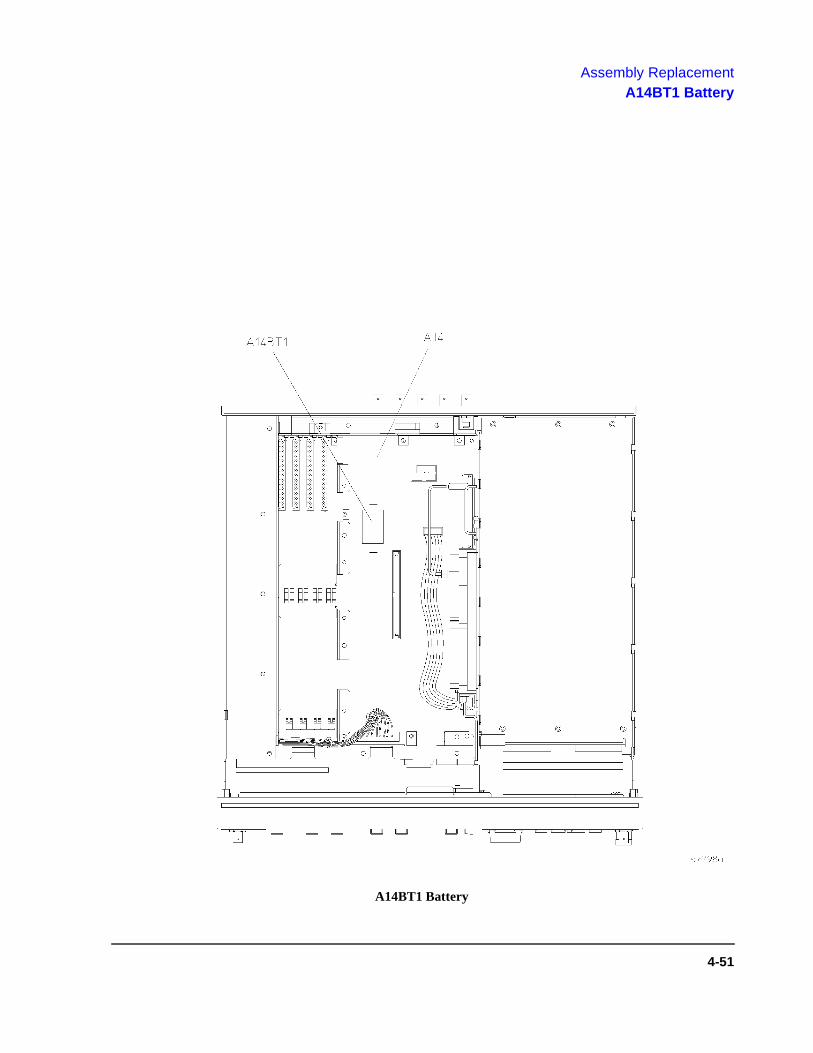
Assembly ReplacementA14BT1 Battery
A14BT1 Battery
4-51

Assembly ReplacementA15 Daughterboard
A15 Daughterboard
Tools Required• T-8 TORX screwdriver• T-10 TORX screwdriver• long nose pliers
Removal1. Remove the instrument cover. (Refer to "Instrument Cover" in this chapter.)
2. Remove the top cover by removing the 11 screws that secure it.
3. Disconnect W1, W2, W6, W7, and W8 from the daughterboard (A15).
4. Remove the right-side cover (not shown) by first removing the four screws that attach it to the instrument chassis. Then push down on the cover while sliding it towards the front of the instrument to unhook its tabs from the slots on the top of the chassis.
4-52

Assembly ReplacementA15 Daughterboard
A15 Daughterboard (1 of 2)
4-53

Assembly ReplacementA15 Daughterboard
5. Simultaneously lift the left and right extractors (item 1) on the output board (A9).
6. Remove the output board from the card cage slot.
7. Repeat steps 5 and 6 for the reference board (A11) and the synthesizer/doubler board (A12).
8. Remove the five screws (item 2) that attach the daughterboard (A15) to instrument chassis.
9. Remove the daughterboard.
Replacement1. Reverse the removal procedure and do the following:
• Torque all T-8 TORX screws to 9 in-lbs.
• Torque all T-10 TORX screws to 9 in-lbs.
• Refer to Chapter 3, "Replaceable Parts," to verify that the cables are reconnected in the correct locations.
4-54

Assembly ReplacementA15 Daughterboard
A15 Daughterboard (2 of 2)
4-55
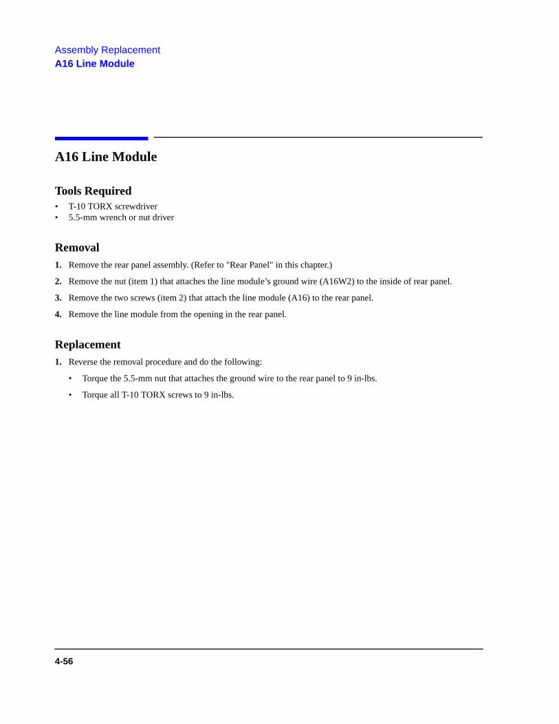
Assembly ReplacementA16 Line Module
A16 Line Module
Tools Required• T-10 TORX screwdriver• 5.5-mm wrench or nut driver
Removal1. Remove the rear panel assembly. (Refer to "Rear Panel" in this chapter.)
2. Remove the nut (item 1) that attaches the line module’s ground wire (A16W2) to the inside of rear panel.
3. Remove the two screws (item 2) that attach the line module (A16) to the rear panel.
4. Remove the line module from the opening in the rear panel.
Replacement1. Reverse the removal procedure and do the following:
• Torque the 5.5-mm nut that attaches the ground wire to the rear panel to 9 in-lbs.
• Torque all T-10 TORX screws to 9 in-lbs.
4-56

Assembly ReplacementA16 Line Module
A16 Line Module
4-57

Assembly ReplacementA17 Rear Panel Interface Board (Options 1EH, UN3, UN4)
A17 Rear Panel Interface Board (Options 1EH, UN3, UN4)
Tools Required• 5/8-inch wrench or nut driver• 1/4-inch wrench or nut driver (Option 1EM)
Removal1. Remove the rear panel assembly. (Refer to "Rear Panel" in this chapter.)
2. Remove the nuts (item 1) and washers (item 2) on the eight BNC connectors of the rear panel.
If you have Option 1EM, remove the nuts (item 3) and washers (item 4) on eight of the associated SMB connectors on the rear panel.
3. Remove the rear panel interface board (A17) from the rear panel.
Replacement1. Reverse the removal procedure and do the following:
• Torque the 5/8-inch BNC nuts to 21 in-lbs.
• If you have Option 1EM, torque the 1/4-inch SMB nuts to 14 in-lbs.
4-58
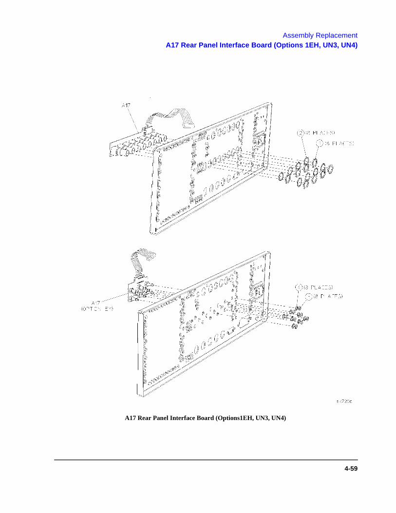
Assembly ReplacementA17 Rear Panel Interface Board (Options 1EH, UN3, UN4)
A17 Rear Panel Interface Board (Options1EH, UN3, UN4)
4-59

Assembly ReplacementAT1 Electronic Attenuator/RPP
AT1 Electronic Attenuator/RPP
Tools Required• T-10 TORX screwdriver• 5/16-inch open-end wrench
Removal1. Remove the instrument cover. (Refer to "Instrument Cover" in this chapter.)
2. Remove the top cover by removing the 11 screws that secure it.
3. Disconnect W9, W13, and W14 from the electronic attenuator/RPP (AT1).
4. Remove the two screws (item 1) that attach the attenuator/RPP to the instrument chassis.
5. Tilt the attenuator/RPP away from the chassis wall, then carefully lift it out of the instrument.
There are two hinged tabs at the bottom of the attenuator/RPP which fit into slots in the instrument chassis. Therefore, it is necessary to tilt the attenuator/RPP away from the chassis wall so that the tabs can be guided out of the slots.
Replacement1. Reverse the removal procedure and do the following:
• When reinstalling the electronic attenuator/RPP (AT1), remember to insert its hinged tabs into the slots located at the base of the chassis wall on which the attenuator/RPP will be mounted.
• Torque W9 and W14 to 9 in-lbs.
• Torque the two T-10 TORX screws to 9 in-lbs.
4-60

Assembly ReplacementAT1 Electronic Attenuator/RPP
AT1 Electronic Attenuator/RPP
4-61

Assembly ReplacementB1 Small Fan Assembly
B1 Small Fan Assembly
Tools Required• knife blade (or equivalent)• long nose pliers
Removal
NOTE: It is best to attempt this procedure without removing the front panel assembly. If the front panel assembly is removed, you will be required to perform time-consuming “Power Level Accuracy” verification tests and adjustments.
1. Remove the instrument cover. (Refer to "Instrument Cover" in this chapter.)
2. Disconnect B1W1 from the motherboard (A14).
3. Remove the four plastic rivets (item 1) that attach the fan assembly (B1) to the instrument chassis. Use a knife blade (or equivalent) to pry up the head of the plunger portion of the rivet. Once the head of the plunger is adequately raised, use a pair of long nose pliers to remove the rivet. Be careful not to damage the rivets with the blade.
NOTE: The plastic rivets consist of two pieces: a plunger and a sheath. Ensure both parts are removed.
4. Remove the fan assembly.
Replacement1. Reverse the removal procedure. When reinserting the plastic rivets, the sheath must be fully seated in the fan
assembly before the plunger can be depressed.
4-62

Assembly ReplacementB1 Small Fan Assembly
B1 Small Fan Assembly
4-63

Assembly ReplacementB2 Large Fan Assembly
B2 Large Fan Assembly
Tools Required• 1/4-inch open-end wrench• Modified T-10 TORX bit (HP part number 8710-1637)
Bit Modification. The hexagonal head at the end of the TORX bit must be removed so that the total length of the bit is approximately 1.5 inches (see figure below). A hexagonal portion of the bit will remain for use with a wrench. The shortened bit will now fit between the fan assembly and the front panel assembly.
Removal
NOTE: It is best to attempt this procedure without removing the front panel assembly. If the front panel assembly is removed, you will be required to perform time-consuming “Power Level Accuracy” verification tests and adjustments.
1. Remove the instrument cover. (Refer to "Instrument Cover" in this chapter.)
2. Disconnect B2W1 from the motherboard (A14).
3. Remove the four screws (item 1) that attach the fan assembly (B2) to the instrument chassis.
4. Remove the fan assembly.
Replacement1. Reverse the removal procedure and torque the T-10 TORX screws to 9 in-lbs.
4-64

Assembly ReplacementB2 Large Fan Assembly
B2 Large Fan Assembly
4-65

Assembly ReplacementW11, W12, and W14 Semi-Rigid Cables
W11, W12, and W14 Semi-Rigid Cables
Tools Required• MILBAR 2R snap-ring pliers (used to remove snap rings from cable retainers)• 5/16-inch open-end wrench
Removal1. Remove all the daughterboard card cage boards to allow access to the instrument chassis cable connections. (Refer
to "A9, A11, and A12 Daughterboard Card Cage Boards" in this chapter.)
2. Remove the snap ring (item 1) from the cable retainer (item 2) of the cable you want to remove. The cable is now disconnected from the instrument chassis (item 3).
3. Disconnect the other end of the cable.
Replacement1. If you’re installing a new cable, a new cable retainer (item 2) must first be attached to the end of the cable (item 4).
Verify the cable retainer is correctly attached by listening for an audible “click” as you slide it over the end of the cable.
2. Insert the cable-retainer end of the cable assembly into the opening of the instrument chassis and then secure it with a snap ring.
3. Connect the other end of the cable. All semi-rigid cables should be torqued to 9 in-lbs.
4. Replace the daughterboard card cage boards.
4-66
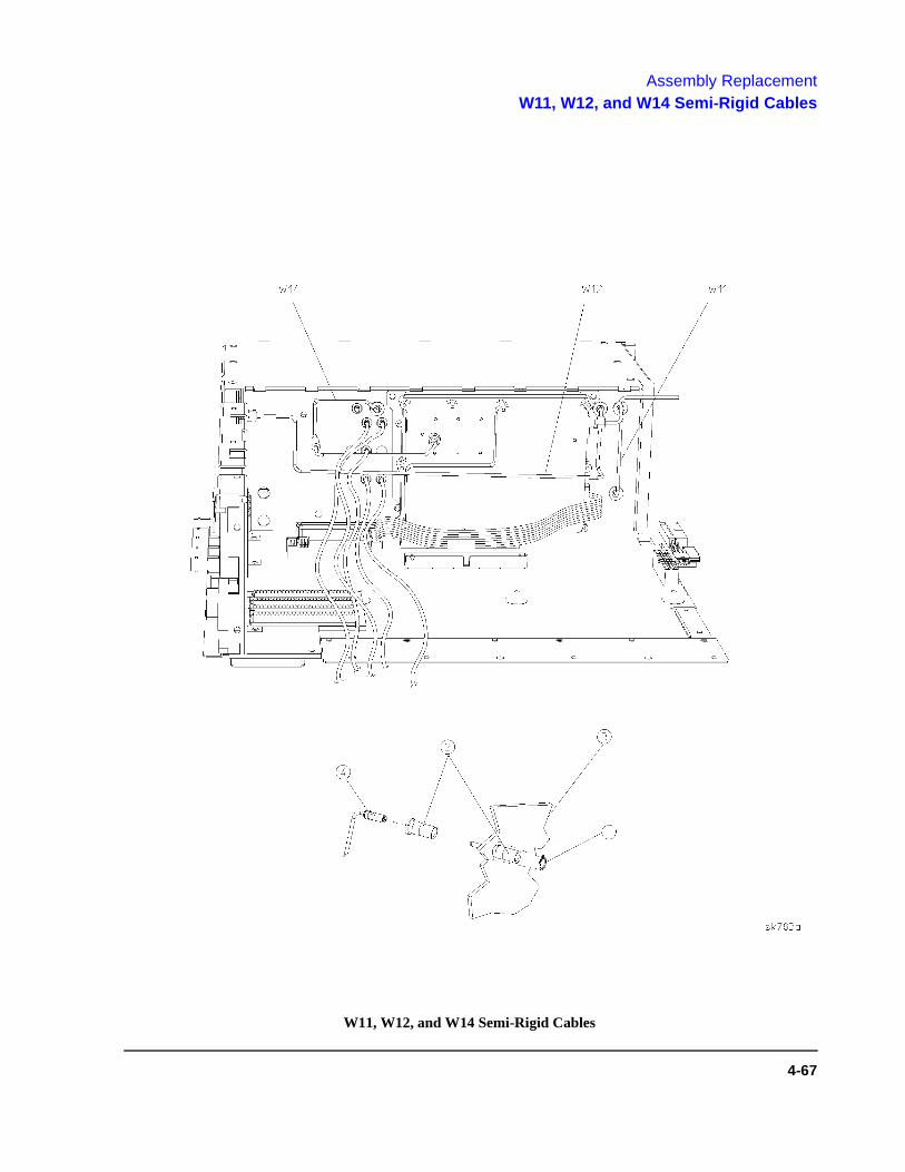
Assembly ReplacementW11, W12, and W14 Semi-Rigid Cables
W11, W12, and W14 Semi-Rigid Cables
4-67

Assembly ReplacementW11, W12, and W14 Semi-Rigid Cables
4-68

5 Post-Repair Procedures
This chapter lists the performance tests and adjustments that must be performed after an assembly has been replaced.
5-1
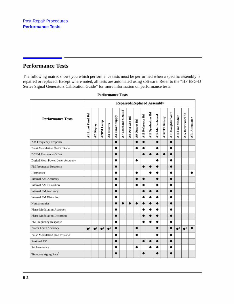
Post-Repair ProceduresPerformance Tests
Performance Tests
The following matrix shows you which performance tests must be performed when a specific assembly is repaired or replaced. Except where noted, all tests are automated using software. Refer to the “HP ESG-D Series Signal Generators Calibration Guide” for more information on performance tests.
Performance Tests
Performance Tests
Repaired/Replaced Assembly
A1
Fro
nt P
anel
Bd
A2
Dis
play
A2D
S1 L
amp
A3
Inve
rter
A4
Pow
er S
uppl
y
A7
Bas
eban
d G
en B
d
A8
Dat
a G
en B
d
A9
Out
put
Bd
A11
Ref
eren
ce B
d
A12
Syn
thes
izer
Bd
A14
Mot
herb
oard
A14
BT
1 B
atte
ry
A15
Dau
ghte
rboa
rd
A16
Lin
e M
odul
e
A17
Rea
r P
anel
Bd
AT
1 A
tten
uato
r
AM Frequency Response ● ● ● ● ●
Burst Modulation On/Off Ratio ● ● ● ● ●
DCFM Frequency Offset ● ● ● ● ● ●
Digital Mod: Power Level Accuracy ● ● ● ●
FM Frequency Response ● ● ● ● ●
Harmonics ● ● ● ● ● ●
Internal AM Accuracy ● ● ● ● ●
Internal AM Distortion ● ● ● ● ●
Internal FM Accuracy ● ● ● ● ●
Internal FM Distortion ● ● ● ● ●
Nonharmonics ● ● ● ● ● ● ● ●
Phase Modulation Accuracy ● ● ● ● ●
Phase Modulation Distortion ● ● ● ● ●
PM Frequency Response ● ● ● ● ●
Power Level Accuracy ●1 ●1 ●1 ●1 ● ● ● ● ●2 ●2 ●
Pulse Modulation On/Off Ratio ● ● ● ●
Residual FM ● ● ● ● ●
Subharmonics ● ● ● ● ●
Timebase Aging Rate3 ● ● ● ●
5-2

Post-Repair ProceduresPerformance Tests
Modulation Source Frequency Accuracy3 ● ● ●
Digital Mod: Internal IQ Quality ● ● ● ● ● ● ● ●
Relative Power Level Accuracy ● ● ● ● ●
1. Perform this test only if you do not have Option 1EM.
2. Perform this test only if you have Option 1EM.
3. This test must be performed manually.
Performance Tests
Performance Tests
Repaired/Replaced Assembly
A1
Fro
nt P
anel
Bd
A2
Dis
play
A2D
S1 L
amp
A3
Inve
rter
A4
Pow
er S
uppl
y
A7
Bas
eban
d G
en B
d
A8
Dat
a G
en B
d
A9
Out
put
Bd
A11
Ref
eren
ce B
d
A12
Syn
thes
izer
Bd
A14
Mot
herb
oard
A14
BT
1 B
atte
ry
A15
Dau
ghte
rboa
rd
A16
Lin
e M
odul
e
A17
Rea
r P
anel
Bd
AT
1 A
tten
uato
r
5-3

Post-Repair ProceduresAdjustments
Adjustments
The following matrix shows you which adjustments must be performed when a specific assembly is repaired or replaced. Except where noted, all adjustments are automated using software. Refer to the “HP ESG-D Series Signal Generators Calibration Guide” for more information on adjustments.
Adjustments
Adjustments
Repaired/Replaced Assembly
A1
Fro
nt P
anel
Bd
A2
Dis
play
A2D
S1 L
amp
A3
Inve
rter
A4
Pow
er S
uppl
y
A7
Bas
eban
d G
en B
d
A8
Dat
a G
en B
d
A9
Out
put
Bd
A11
Ref
eren
ce B
d
A12
Syn
thes
izer
Bd
A14
Mot
herb
oard
A14
BT
1 B
atte
ry
A15
Dau
ghte
rboa
rd
A16
Lin
e M
odul
e
A17
Rea
r P
anel
Bd
AT
1 A
tten
uato
r
ABUS ADC Cal ● ●
Internal Source Cal ● ● ●
VCO Bias Adjustment ● ● ●
Lock Angle Adjustment ● ● ●
Kv vs Frequency Cal ● ● ●
AM Audio Path Offset ● ● ● ●
Timebase DAC Cal ● ● ●
FM Scale DAC Offset Cal ● ● ● ●
FM Path Offset Cal ● ● ● ●
FM In-band DAC Offset Cal ● ● ● ●
FM Invert Amp Offset Cal ● ● ● ●
FM1/2 Path Ratio Gain Cal ● ● ● ●
Mod Source Relative Gain Cal ● ● ● ●
FM Delay Pot Adjustment ● ● ● ●
Wide BW PM Cal ● ● ● ●
DCFM Cal ● ● ● ● ●
Peak Detector Cal ● ● ● ●
Normal Mode PM Cal ● ● ● ●
Burst Modulator Cal ● ● ●
FM Out-of Band Cal ● ● ● ●
5-4
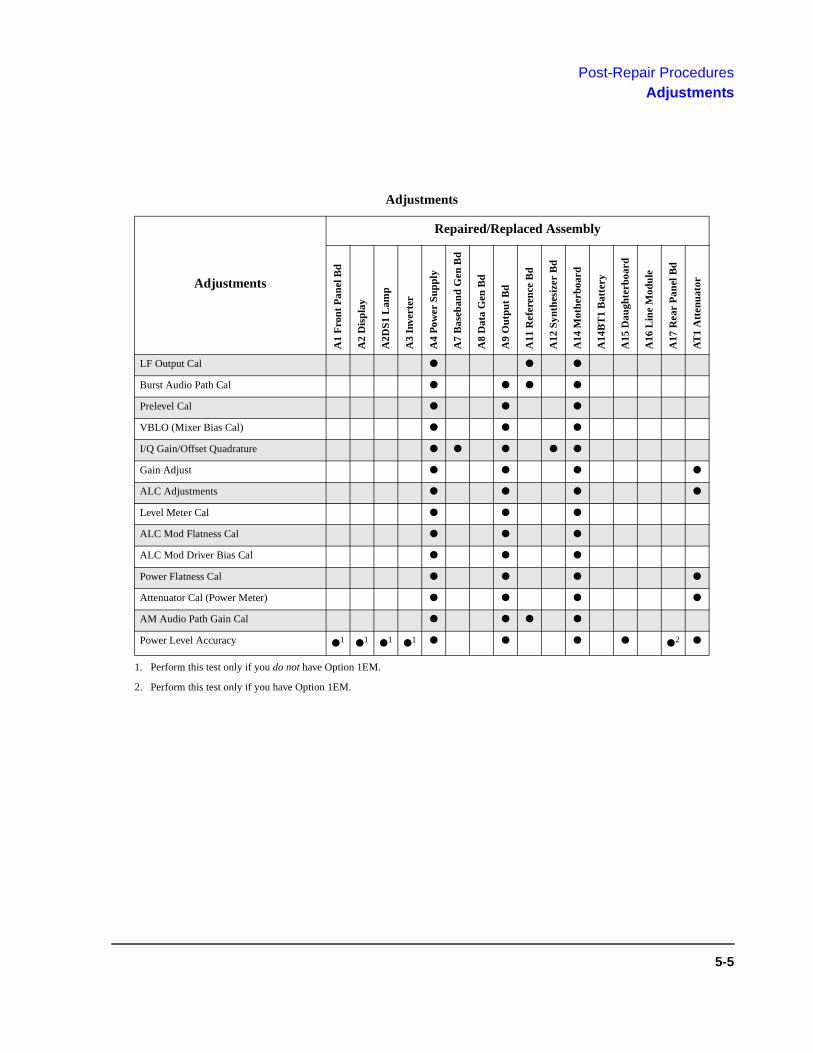
Post-Repair ProceduresAdjustments
LF Output Cal ● ● ●
Burst Audio Path Cal ● ● ● ●
Prelevel Cal ● ● ●
VBLO (Mixer Bias Cal) ● ● ●
I/Q Gain/Offset Quadrature ● ● ● ● ●
Gain Adjust ● ● ● ●
ALC Adjustments ● ● ● ●
Level Meter Cal ● ● ●
ALC Mod Flatness Cal ● ● ●
ALC Mod Driver Bias Cal ● ● ●
Power Flatness Cal ● ● ● ●
Attenuator Cal (Power Meter) ● ● ● ●
AM Audio Path Gain Cal ● ● ● ●
Power Level Accuracy ●1 ●1 ●1 ●1 ● ● ● ● ●2 ●
1. Perform this test only if you do not have Option 1EM.
2. Perform this test only if you have Option 1EM.
Adjustments
Adjustments
Repaired/Replaced Assembly
A1
Fro
nt P
anel
Bd
A2
Dis
play
A2D
S1 L
amp
A3
Inve
rter
A4
Pow
er S
uppl
y
A7
Bas
eban
d G
en B
d
A8
Dat
a G
en B
d
A9
Out
put
Bd
A11
Ref
eren
ce B
d
A12
Syn
thes
izer
Bd
A14
Mot
herb
oard
A14
BT
1 B
atte
ry
A15
Dau
ghte
rboa
rd
A16
Lin
e M
odul
e
A17
Rea
r P
anel
Bd
AT
1 A
tten
uato
r
5-5

Post-Repair ProceduresAdjustments
5-6

6 Error Messages
This chapter explains the error messages that might be shown on the front panel display or transmitted over the interface bus.
6-1

Error MessagesError Messages
Error Messages
If an error condition occurs in the signal generator, it will always be reported to both the front panel display error queue and the SCPI (remote interface) error queue. These two queues are viewed and managed separately.
The Front Panel Error Queue
This queue is designed in a circular (rotating) fashion. It can hold up to 30 error messages. If the queue is full, and additional error messages arrive, the oldest errors are lost. The previously read messages are not cleared from the queue; they remain in the queue until they are overwritten by a new error message.
The front panel error queue information can be accessed by pressing Utility, Error Info. From the Error Info menu, you may choose from View Previous Error Message, View Next Error Message, or Clear Error
Queue(s). You can also use the RPG and the arrow keys to review the messages/
If there are any unviewed messages in the front panel error queue, the ERR annunciator will be activated on the signal generator’s display. you can optionally rotate the RPG or use the arrow keys to view the error messages. To empty the queue, press Utility, Error Info, Clear Error Queue(s).
There are some special error types called permanent errors. These include unlock, ovencold, hi/lo, etc. Permanent errors remain in the error queues until the error condition is cleared. Pressing Utility, Error
Info, Clear Error Queue(s) will empty the front panel error queue, but the permanent errors will be re-reported if the error condition(s) still exist.
The SCPI Remote Interface Error Queue
This queue is constructed in a linear first-in/first-out fashion. It can hold up to 30 error messages. As errors and events are detected, they are placed in the queue. Unlike the front panel error queue, errors in this queue are not overwritten by the latest incoming error messages. If the queue overflows, the last error in the queue is replaced with the error:
-350,Queue overflow
When the queue overflows, the least recent errors remain in the queue, and the most recent error is discarded. Reading an error from the head of the queue removes that error from the queue, and opens a position in the tail of the queue for a new error, if one is subsequently detected.
6-2

Error MessagesError Messages
When all the errors have been read from the queue, further error queries will return:
0,No error
The SCPI query SYSTem:ERRor? is used to view messages in the SCPI error queue. The error queue will be cleared when any of the following occur (IEEE 488.2, section 11.4.3.4):
• Upon power up
• Upon receipt of a *CLS command
• Upon reading the last item from the queue
In the SCPI error queue, the permanent errors are re-reported after the message 0, No error is read using the SYSTem:ERRor? query and after the *CLS command is executed.
6-3

Error MessagesQuerying the Error Queue
Querying the Error Queue
The queue query message is a request for the next entry from the instrument’s error queue. This queue contains an integer that can range from 32768 to 32767. Negative error numbers are reserved by the SCPI standard and are defined in this section. Positive error numbers are instrument-dependent. An error value of zero indicates that no error or event has occurred.
The signal generator responds to the SYSTem:ERRor? (or STATus:QUEue?) query using the following form:
<error number>, <error description>
The <error number> is a unique error descriptor. Certain standard error numbers are described in this section. The <error description> is a short description of the error, (optionally) followed by additional information regarding the error. Short descriptions of the standard error numbers are described in this section. The information that follows the error message may contain corrective actions that should be followed to correct the error condition.
The <device-dependent info> section of the response may contain information which will allow you to determine the exact error and context. For example:
-131, Invalid suffix;FREQuency:CENT 2.0E+5 dBmV
The maximum string length of <error description> plus <device-dependent info> is 255 characters. The <error description> will be sent exactly as indicated in this document, including case.
If there has been no error, that is, if the queue is empty, the signal generator will respond with:
0, No error
If there has been more than one error, the instrument will respond with the first one in its queue. Subsequent responses to SYSTem:ERRor? will continue with the queue until it is empty.
6-4

Error MessagesError Numbers
Error Numbers
The system-defined error numbers are chosen on an enumerated (“1 of N”) basis. The SCPI-defined error numbers and the <error_description> portions of the error query response are listed here. The first error described in each class (for example, 100, 200, 300, 400) is a “generic” error. In selecting the proper error number to report, more specific error codes are preferred.
6-5

Error MessagesNo Error
No Error
This message indicates that the error queue contains no errors.
Error Number Error Description [description/explanation/examples]
0 No error
The queue is empty. Every error in the queue has been read or the queue was purposely cleared by power-on or *CLS.
6-6

Error MessagesSCPI Standard Error Messages
SCPI Standard Error Messages
Error Message Description
The list of error messages in this chapter describes all of the SCPI error messages associated with signal generator operation. A sample error message description is provided below to help you understand how information will be presented in this section.
-222 Data out of range;value clipped to lower limit.
Indicates that the user has entered a deviation, depth or internal source frequency that is beyond the specified limits.
The following list explains each element of the sample error message listing shown above.
• SCPI Error Number - The standard SCPI error number (222 in this example). Standard SCPI error numbers are always negative, with the exception of 0, No error.
• SCPI Error Message - The SCPI error message is Data out of range; in this example.
• Detailed Description - The information that appears after the semicolon (;) provides more detail as to the exact nature of the error. In this example, value clipped to lower limit tells you that you have entered a value outside the allowable range and the signal generator has changed the value so that it falls within the allowable limits. If no detailed description exists, it will be omitted from the error message.
• Explanation/Action Required - The text that appears below each error message listing contains an explanation of the error message and, in some cases, corrective actions that should be followed in order to correct the error condition. Though this information is not shown on the signal generator’s display, it can be found in the following section.
6-7
Error MessagesCommand Error
Command Error
An error number in the range [199 to 100] indicates that an IEEE 488.2 syntax error has been detected by the instrument’s parser. The occurrence of any error in this class will cause the command error bit (bit 5) in the event status register (IEEE 488.2, section 11.5.1) to be set. If this bit is set, one of the following events has occurred:
• An IEEE 488.2 syntax error has been detected by the parser. That is, a control-to-device message was received which is in violation of the IEEE 488.2 standard. Possible violations include a data element which violates device listening formats or whose type is unacceptable to the device.
• An unrecognized header was received. Unrecognized headers include incorrect device-specific headers and incorrect or unimplemented IEEE 488.2 common commands.
Events that generate command errors will not generate execution errors, device-specific errors, or query errors; see the error definitions in this chapter.
Command Error Message Descriptions
This section lists the signal generator’s command error messages and their associated descriptions.
Error Number Error Description [description/explanation/examples]
-100 Command error
This is a generic syntax error for devices that cannot detect more specific errors. The code indicates only that a command error as defined in IEE 488.2, 11.5.1.1.4 has occurred.
-101 Invalid character
A syntactic command contains a character which is invalid for that type. For example, a header containing an ampersand, SETUP&. This error might be used in place of error numbers 114, 121, 141 and some others.
-102 Syntax error
An unrecognized command or data type was encountered. For example, a string was received when the device does not accept strings.
-103 Invalid separator
The parser was expecting a separator and encountered an illegal character. For example, the semicolon was omitted after a program message unit.
6-8
Error MessagesCommand Error
-104 Data type error
The parser recognized a data element that is not allowed. For example, numeric or string data was expected, but block data was encountered.
-105 GET not allowed
A Group Execute Trigger was received within a program message (see IEEE 488.2, 7.7). Correct the HP-IB controller program so that the GET does not occur within a line of HP-IB program code.
-108 Parameter not allowed
More parameters were received than expected for the header. For example, the *ESE common command only accepts one parameter, so receiving *ESE 0,1 is not allowed.
-109 Missing parameter
Fewer parameters were received than required for the header. For example, the *ESE common command requires one parameter, so receiving *ESE is not allowed.
-110 Command header error
An error was detected in the header. This message is used when the device cannot detect the more specific errors described for errors 111 through 119.
-111 Header separator error
A character which is not a legal header separator was encountered while parsing the header.
-112 Program mnemonic too long
The header contains more than twelve characters (see IEEE 488.2, 7.6.1.4.1).
-113 Undefined header
The header is syntactically correct, but it is undefined for this specific device. For example, *XYZ is not defined for any device.
-114 Header suffix out of range
The value of a header suffix attached to a program mnemonic makes the header invalid.
-120 Numeric data error
This error, as well as errors 121 through 129, are generated when parsing a data element which appears to be numeric, including non-decimal numeric types. This particular error message is used if the device cannot detect a more specific error.
6-9
Error MessagesCommand Error
-121 Invalid character in number
An invalid character for the data type being parsed was encountered. For example, an alpha in a decimal numeric or a “9” in octal data.
-123 Exponent too large
The magnitude of an exponent was greater than 32000 (see IEEE 488.2, 7.7.2.4.1).
-124 Too many digits
The mantissa of a decimal-numeric data element contained more than 255 digits excluding leading zeros (see IEEE 488.2, 7.7.2.4.1).
-128 Numeric data not allowed
A legal numeric data element was received, but the device does not accept one in this position for the header.
-130 Suffix error
This error, as well as errors 131 through 139, are generated when parsing a suffix. This particular error message is used if the device cannot detect a more specific error.
-131 Invalid suffix
The suffix does not follow the syntax described in IEEE 488.2, 7.7.3.2, or the suffix is inappropriate for this device.
-134 Suffix too long
The suffix contained more than twelve characters (see IEEE 488.2, 7.7.3.4).
-138 Suffix not allowed
A suffix was encountered after a numeric element which does not allow suffixes.
-140 Character data error
This error, as well as errors 141 through 149, are generated when parsing a character data element. This particular error message is used if the device cannot detect a more specific error.
-141 Invalid character data
Either the character data element contains an invalid character or the particular element received is not valid for the header.
-144 Character data too long
The character data element contains more that twelve characters (see IEEE 488.2, 7.7.1.4).
6-10

Error MessagesCommand Error
-148 Character data not allowed
A legal character data element was encountered where prohibited by the device.
-150 String data error
This error, as well as errors 151 through 159, are generated when parsing a string data element. This particular error message is used if the device cannot detect a more specific error.
-151 Invalid string data
A string data element was expected, but was invalid (see IEEE 488.2, 7.7.5.2). For example, an END message was received before the terminal quote character.
-158 String data not allowed
A string data element was encountered, but not allowed by the device at this point in the parsing.
-160 Block data error
This error, as well as errors 161 through 169, are generated when parsing a block data element. This particular error message is used if the device cannot detect a more specific error.
-161 Invalid block data
A block data element was expected, but was invalid (see IEEE 488.2, 7.7.6.2). For example, an END message was received before the end length was satisfied.
-168 Block data not allowed
A legal block data element was encountered, but not allowed by the device at this point in the parsing.
-170 Expression data error
This error, as well as errors 171 through 179, are generated when parsing an expression data element. This particular error message is used if the device cannot detect a more specific error.
-171 Invalid expression
The expression data element was invalid (see IEEE 488.2, 7.7.7.2). For example, unmatched parentheses or an illegal character.
-178 Expression data not allowed
A legal expression data was encountered, but was not allowed by the device at this point in parsing.
6-11

Error MessagesCommand Error
-180 Macro error
This error, as well as errors 181 through 189, are generated when defining a macro or executing a macro. This particular error message is used if the device cannot detect a more specific error.
-181 Invalid outside macro definition
Indicates that a macro parameter placeholder ($<number) was encountered outside of a macro definition.
-183 Invalid inside macro definition
Indicates that the program message unit sequence, sent with a *DDT or a *DMC command, is syntactically invalid (see IEEE 488.2, 10.7.6.3).
-184 Macro parameter error
Indicates that a command inside the macro definition had the wrong number or type of parameters.
6-12
Error MessagesExecution Error
Execution Error
An error number in the range [299 to 200] indicates that an error has been detected by the instrument’s execution control block. The occurrence of any error in this class will cause the execution error bit (bit 4) in the event status register (IEEE 488.2, section 11.5.1) to be set. If this bit is set, one of the following events has occurred:
• A <PROGRAM DATA> element following a header was evaluated by the device as outside of its legal input range or is otherwise inconsistent with the device’s capabilities.
• A valid program message could not be properly executed due to some device condition.
Execution errors will be reported by the device after rounding and expression evaluation operations have been completed. Rounding a numeric data element, for example, will not be reported as an execution error. Events that generate execution errors will not generate command errors, device-specific errors, or query errors; see the error definitions in this chapter.
Execution Error Message Descriptions
This section lists the signal generator’s execution error messages and their associated descriptions.
Error Number Error Description [description/explanation/examples]
-200 Execution Error
This is a generic syntax error for devices that cannot detect more specific errors. The code indicates only that an execution error as defined in IEEE 488.2, 11.5.1.1.5 has occurred.
-201 Invalid while in local
Indicates that a command is not executable while the device is in local mode due to a hard local control (see IEEE 488.2, 5.6.1.5). For example, a device with a rotary switch receives a message which would change the switch’s state, but the device is in local so the message cannot be executed.
-202 Settings lost due to rtl
Indicates that a setting associated with a hard local control (see IEEE 488.2, 5.6.15) was lost when the device changed to LOCS from REMS or to LWLS from RWLS.
-210 Trigger error
Indicates that a GET, *TRG, or a triggering signal could not be executed due to an error.
6-13

Error MessagesExecution Error
-211 Trigger ignored
Indicates that a GET, *TRG, or triggering signal was received and recognized by the device, but was ignored because of device timing considerations. For example, the device was not ready to respond.
-212 Arm ignored
Indicates that an arming signal was received and recognized by the device but was ignored.
-213 Init ignored
Indicates that a request for a measurement initiation was ignored as another measurement was already in progress.
-214 Trigger deadlock
Indicates that a trigger source for the initiation of a measurement is set to GET and a subsequent measurement query is received. The measurement cannot begin until a GET is received, but the GET would cause an INTERRUPTED error.
-215 Arm deadlock
Indicates that the arm source for the initiation of a measurement is set to GET and a subsequent measurement query is received. The measurement cannot begin until a GET is received, but the GET would cause an INTERRUPTED error.
-220 Parameter error
Indicates that a program data element related error has occurred. This particular error message is used if the device cannot detect a more specific errors described for errors221 through 229.
-221 Settings conflict
Indicates that a legal program data element was parsed but could not be executed due to the current device state (see IEEE 488.2 11.5.1.1.5).
-222 Data out of range
Indicates that a legal program data element was parsed but could not be executed because the interpreted value was outside the legal range defined by the device (see IEEE 488.2 11.5.1.1.5).
-223 Too much data
Indicates that a legal program data element of block, expression or string type was received that contained more data than the device could handle due to memory or related device-specific requirements.
6-14

Error MessagesExecution Error
-224 Illegal parameter value
Used where exact value, from a list of possibilities, was expected.
-225 Out of memory
The device has insufficient memory to perform the requested operation.
-226 Lists not same length
Attempted to use LIST structure having individual LISTs of unequal length.
-230 Data corrupt or stale
Possibly invalid data. A new reading was started but not completed since last access.
-231 Data questionable
Indicates that the measurement accuracy is questionable.
-232 Invalid format
Indicates that a legal program data element was parsed but could not be executed because the data format or structure is inappropriate. For example, when loading memory tables or when sending a SYSTem:SET parameter for an unknown instrument.
-233 Invalid version
Indicates that a legal program data element was parsed but could not be executed because the version of the data is incorrect to the device. This particular error is used when file or block data elements are recognized by the instrument, but cannot be executed for reasons of version incompatibility. For example, a non- supported file version or a non- supported instrument version.
-240 Hardware error
Indicates that a legal program command or query could not be executed because of a hardware problem in the device. The definition of what constitutes a hardware problem is completely device-specific. This error is used when the device cannot detect the more specific errors described for errors 241 through 249.
-241 Hardware missing
Indicates that a legal program command or query could not be executed because of missing device hardware. For example, an option was not installed.
-250 Mass storage error
Indicates that a mass storage error has occurred. This message is used when a device cannot detect the more specific errors described for errors 251 through 259.
6-15
Error MessagesExecution Error
-252 Missing media
Indicates that a legal program command or query could not be executed because of missing media, for instance no disk in the disk drive. The definition of what constitutes missing media is device-specific.
-253 Corrupt media
Indicates that a legal program command or query could not be executed because of corrupt media, for instance a bad disk or incorrect disk format. The definition of what constitutes corrupt media is device-specific.
-254 Media full
Indicates that a legal program command or query could not be executed because the media was full. For example, there is was no space left on the disk. The definition of what constitutes full media is device-specific.
-255 Directory full
Indicates that a legal program command or query could not be executed because the media directory was full. The definition of what constitutes a full media directory is device-specific.
-256 File name not found
Indicates that a legal program command or query could not be executed because the file name on the device media could not be found. For example, an attempt was made to read or copy a nonexistent file. The definition of what constitutes a file not being found is device-specific.
-257 File name error
Indicates that a legal program command or query could not be executed because a file name on the device media was in error. For example, an attempt was made to copy to a duplicate filename. The definition of what constitutes a file name error is device-specific.
-258 Media protected
Indicates that the device or user has attempted to write to a read-only memory subsystem (msus). The definition of a protected media is device-specific.
-260 Expression error
Indicates that an expression data element-related error occurred. This error message is used when the device cannot detect the more specific errors described for errors 261 through 269.
6-16

Error MessagesExecution Error
-261 Math error in expression
Indicates that a syntactically legal expression program data element could not be executed due to a math error. For example, a divide-by-zero was attempted. The definition of a math error is device-specific.
-270 Macro error
Indicates that a macro-related execution error occurred. This error message is used when the device cannot detect the more specific errors described for errors 271 through 279.
-271 Macro syntax error
Indicates that a syntactically legal macro program data sequence, written in accordance with IEEE 488.2, 10.7.2, could not be executed due to a syntax error within the macro definition (see IEEE 488.2, 10.7.6.3).
-272 Macro execution error
Indicates that a syntactically legal macro program data sequence could not be executed due to an error within the macro definition (see IEEE 488.2, 10.7.6.3).
-273 Illegal macro label
Indicates that the macro label defined in the *DMC command was a legal string syntax, but could not be accepted by the device (see IEEE 488.2, 10.7.3 and 10.7.6.2). For example, the label was too long, the same as a common command header, or contained invalid header syntax.
-274 Macro parameter error
Indicates that the macro definition improperly used a macro parameter placeholder (see IEEE 488.2, 10.7.3).
-275 Macro definition too long
Indicates that a syntactically legal macro program data sequence could not be executed because the string or block contents were too long for the device to handle (see IEEE 488.2, 10.7.6.1).
-276 Macro recursion error
Indicates that a syntactically legal macro program data sequence could not be executed because the device found it to be recursive (see IEEE 488.2, 10.7.6.4).
-277 Macro redefinition not allowed
Indicates that the macro label defined in the *DMC command could not be executed because the macro label was already defined (see IEEE 488.2, 10.7.6.4).
6-17

Error MessagesExecution Error
-278 Macro header not found
Indicates that a syntactically legal macro label in the *GMC? query could not be executed because the header was not previously defined.
-280 Program error
Indicates that a downloaded program-related execution error occurred. This error message is used when the device cannot detect the more specific errors described for errors 281 through 289. The syntax used in a program and the mechanism for downloading a program is device-specific.
-281 Cannot create program
Indicates that an attempt to create a program was unsuccessful. This may be due to insufficient memory.
-282 Illegal program name
Indicates that the name used to reference a program was invalid. For example, redefining an existing program, deleting a nonexistent program, or in general, referencing a nonexistent program.
-283 Illegal variable name
Indicates that an attempt was made to reference a nonexistent variable.
-284 Program currently running
Indicates that certain operation related to programs may be illegal while the program is running. For example, deleting a running program may be illegal.
-285 Program syntax error
Indicates that a syntax error appears within a downloaded program. The syntax used when parsing a downloaded program is device-specific.
-286 Program runtime error
Indicates that a runtime error was detected in a downloaded program.
-290 Memory use error
Indicates that a user request has directly or indirectly caused an error related to memory or <data_handles>. This is not the same as “bad” memory.
-291 Out of memory
A downloaded program required more memory than was available in the instrument.
6-18
Error MessagesExecution Error
-292 Referenced name does not exist
A downloadecd program attempted to access an undefined element (a variable, constant, filename, etc.).
-293 Referenced name already exists
A downloaded program attempted to define an element (a variable, constant, filename, etc.) that had already been defined.
-294 Incompatible type
Indicates that the type or structure of a memory item is inadequate.
6-19

Error MessagesDevice-specific Error
Device-specific Error
An error number in the range [399 to 300] or [1 to 32767] indicates that the instrument has detected an error which is not a command error, a query error, or an execution error; some device operations did not properly complete, possibly due to an abnormal hardware or firmware condition. These codes are also used for self-test response errors. The occurrence of any error in this class will cause the device-specific error bit (bit 3) in the event status register (IEEE 488.2, section 11.5.1) to be set.
NOTE: For positive error number descriptions see the section titled “ESG-D Series Signal Generator Instrument-Specific Error Messages.”
The meaning of positive error codes is device-dependent and may be enumerated or bit mapped. The <error_message> string for positive error codes is not defined by SCPI. The occurrence of any error in this class will cause the device-specific error bit (bit 3) in the event status register (IEEE 488.2, section 11.5.1) to be set. Events that generate device-specific errors will not generate command errors, or query errors; see the other error definitions in this section.
Device-Specific Error Message Descriptions
This section lists the signal generator’s device-specific error messages and their associated descriptions.
Error Number Error Description [description/explanation/examples]
-300 Device-specific error
This is a generic device-dependent error for devices that cannot detect more specific errors. The code indicates only that a device-dependent error as defined in IEEE 488.2, 11.5.1.1.6 has occurred.
-310 System error
Indicates that an error, termed “system error” by the device, has occurred.
-311 Memory error
Indicates that an error was detected in the device’s memory.
-312 PUD memory lost
Indicates that the protected user data saved by the *PUD command has been lost.
-313 Calibration memory lost
Indicates that non-volatile calibration data has been lost.
6-20

Error MessagesDevice-specific Error
-314 Save/recall memory loss
Indicates that the non-volatile data saved by the *SAV? command has been lost.
-315 Configuration memory lost
Indicates that non-volatile configuration data saved by the device has been lost. The meaning of this error is device-dependent.
-320 Storage fault
Indicates that the firmware detected a fault when using data storage. This error is not an indication of physical damage or failure of any mass storage element.
-321 Out of memory
Indicates that an internal operation needed more memory than was available.
-330 Self-test failed
Indicates that the device has detected a failure during its self-test procedure.
-340 Calibration failed
Indicates that the device has detected a failure during its calibration procedure.
-350 Queue overflow
This is a specific code entered into the queue in lieu of the code that caused the error. This message indicates that there is no more room in the queue and an error occurred but was not recorded.
-360 Communication error
This is the generic communication error for devices that cannot detect the more specific errors described for errors 361 through 363.
-361 Parity error in program message
Indicates that the parity bit was not correct when data was received (for example, an incorrect parity bit on a serial port).
-362 Framing error in program message
Indicates that a stop bit was not detected when data was received (for example, a baud rate mismatch).
6-21

Error MessagesQuery Error
Query Error
An error number in the range [499 to 400] indicates that the output queue control of the instrument has detected a problem with the message exchange protocol described in IEEE 4888.2, chapter 6. The occurrence of any error in this class will cause the query error bit (bit 2) to be set in the event status register (IEEE 488.2, section 11.5.1). These errors correspond to message exchange protocol errors described in IEEE 488.2, 6.5. If a query error occurs one of the following is true:
• An attempt is being made to read data from the output queue when no output is either present or pending.
• Data in the output queue has been lost.
Events that generate query errors will not generate command errors, execution errors, or device-specific errors; see the other error definitions in this section.
Query Error Message Descriptions
This section lists the signal generator’s query error messages and their associated descriptions.
Error Number Error Description [description/explanation/examples]
-400 Query Error
This is a generic query error for devices that cannot detect more specific errors. The code indicates only that a query error as defined in IEE 488.2, 11.5.1.1.7 and 6.3 has occurred.
-410 Query INTERRUPTED
Indicates that a condition causing an INTERRUPTED query error occurred (see IEEE 488.2, 6.3.2.7). For example, a query was followed by DAB or GET before a response was completely sent.
-420 Query UNTERMINATED
Indicates that a condition causing an UNTERMINATED query error occurred (see IEEE 488.2, 6.3.2.2). For example, the device was addressed to talk and an incomplete program message was received.
-430 Query DEADLOCKED
Indicates that a condition causing a DEADLOCKED query error occurred (see IEEE 488.2, 6.3.1.7). For example, both the input buffer and the output buffer are full and the device cannot continue.
6-22
Error MessagesQuery Error
-440 Query UNTERMINATED after indefinite response
Indicates that a query was received in the same program message after a query requesting an indefinite response was executed (see IEEE 488.2, 6.3.7.5).
6-23

Error MessagesESG-D Series Signal Generator Instrument-Specific Error Messages
ESG-D Series Signal Generator Instrument-Specific Error Messages
Some instrument-specific error messages incorporate the negative or “generic” SCPI error number with the addition of device-dependent/instrument-specific (ESG-D Series signal generator-specific) information following the semicolon in the error message.
A positive error number indicates that the instrument has detected an error within the HP-IB system, within the instrument’s firmware or hardware, during the transfer of block data, or during calibration.
Error Number Error Description [description/explanation/examples]
-100 Command error;R0:No standby mode allowed.
Indicates that, in HP 8656/57 compatibility mode, R0 was received via HP-IB. This command is not supported by the compatibility mode.
Command error;Remote active function DN/UP not available.
Indicates that, in HP 8656/57 compatibility mode, either DN or UP was received via HP-IB. These commands are not supported by the compatibility mode.
Command error;LO: No low bandwidth ALC mode allowed.
Indicates that, in HP 8656/57 compatibility mode, LO was received via HP-IB. This command is not supported by the compatibility mode.
-102 Syntax error;Bad HP compatibility language character <character>.
Indicates that, in HP 8656/57 compatibility mode, illegal language input was received.
Syntax error;Bad HP compatibility language token <token>.
Indicates that, in HP 8656/57 compatibility mode, a known command or termination specifier was received when it was not expected. For example, a termination specifier was received with no currently active function.
-213 Init ignored;Unable to sweep due to sweep being in an error state. The sweep error should be fixed.
Indicates that the number of list, power, and/or dwell points are in conflict, or a serious system error has occurred in list/sweep. A previous error report should have described the error that is stalling list/sweep.
Init ignored;Cannot initiate sweep in manual mode.
Indicates that the manual mode is on and therefore the instrument cannot sweep.
6-24

Error MessagesESG-D Series Signal Generator Instrument-Specific Error Messages
Init ignored;Sweep is already initiated.
Indicates that the list/sweep is currently initiated and sweeping, therefore the command is not legal according to SCPI.
Init ignored;Sweep is already continuously initiated.
Indicates that the list/sweep is continuously initiated and sweeping, therefore the command is not legal according to SCPI.
-221 Settings conflict;Cannot have uplink protocols while the control frame is on. Frames 1-17 timeslots changed to downlink.
Indicates that, in TETRA mode, some of the timeslots are set to uplink. When the control frame is turned on in TETRA, all timeslots in all frames must use downlink protocols. The instrument enforces this by reconfiguring the timeslots that are not using downlink protocols when the control frame is switched on.
Settings conflict;Cannot select uplink protocols while the control frame is on. Selection changed to custom.
Indicates that in TETRA mode, an attempt has been made to select uplink protocols while the control frame is switched on. TETRA requires that the control frame be switched off in order to select uplink protocols.
Settings conflict;Continuous protocol timeslots cannot be turned off.
Indicates that a continuous protocol timeslot is switched off while in TETRA mode. When a continuous protocol has been selected for a timeslot in TETRA mode, all of the timeslots must be switched on.
Settings conflict;Continuous & Discontinuous setting conflict. All selected Continuous timeslots are now switched to Discontinuous.
Indicates that while in TETRA mode, an attempt has been made to simultaneously assign continuous and discontinuous protocols to the timeslots. Continuous and discontinuous protocols cannot coexist in TETRA mode. If a discontinuous protocol is selected for any timeslot, all timeslots’ protocols are changed to discontinuous protocols.
Settings conflict;Discontinuous & Continuous setting conflict. All selected Discontinuous timeslots are now switched to Continuous.
Indicates that while in TETRA mode, an attempt has been made to simultaneously assign discontinuous and continuous protocols to the timeslots. Discontinuous and
6-25

Error MessagesESG-D Series Signal Generator Instrument-Specific Error Messages
continuous protocols cannot coexist in TETRA mode. If a continuous protocol is selected for any timeslot, all timeslots’ protocols are changed to continuous protocols.
Settings conflict;Frequency list and dwell list are of unequal size. Set one list equal to size one, or make their sizes equal.
Indicates that the frequency list has more than one element and the dwell list has more than one element, and they are not of equal size. If any of the frequency, power, or dwell lists have more than one element, they must all have the same number of elements. A list of a single element is the same as a list of equal size with the single element repeated the necessary number of times.
Settings conflict;Frequency list and power list are of unequal size. Turn one list off, set one to size one, or make their sizes equal.
Indicates that the frequency list has more than one element and the power list has more than one element, and they are not of equal size. If any of the frequency, power, or dwell lists have more than one element, they must all have the same number of elements. A list of a single element is the same as a list of equal size with the single element repeated the necessary number of times.
Settings conflict;Power list and dwell list are of unequal size. Set one to size one, or make their sizes equal.
Indicates that the dwell list has more than one element and the power list has more than one element, and they are not of equal size. If any of the frequency, power, or dwell lists have more than one element, they must all have the same number of elements. A list of a single element is the same as a list of equal size with the single element repeated the necessary number of times.
Settings conflict;The selected external trigger setting conflicts with the previous setting.
Indicates that the external trigger has been set to positive edge for one trigger source and negative edge for another trigger source.
Settings conflict;I/Q & AM WB cannot be on at the same time.
The modulation types I/Q and AM WB cannot be used at the same time. This error is reported when the user attempts to activate one type of modulation while the other is activated. The modulation type that was most recently requested will be turned on and the modulation that was on at the time will be turned off.
Settings conflict;FM2/PM2 value set greater than FM1/PM1 value. FM1/PM1 changed to match FM2/PM2 value.
The deviation of FM2/PM2 must always be less than or equal to the deviation settings
6-26
Error MessagesESG-D Series Signal Generator Instrument-Specific Error Messages
for FM1/PM1. This error will be reported to the queue when FM1/PM1 is enabled and FM2/PM2 is also enabled and an adjustment to either FM2/PM2 deviation causes the FM2 or PM2 deviation to be greater than the FM1 or PM1 deviation. It will also be reported when FM2/PM2 is being turned on, and the last FM1/PM1 deviation setting is less than the current FM2/PM2 deviation setting. In both cases the FM1/PM1 deviation will be adjusted to match the FM2/PM2 deviation.
Settings conflict;FM1/PM1 value set less than FM2/PM2 value. FM2/PM2 changed to match FM1/PM1 value.
The deviation of FM2/PM2 must always be less than or equal to the deviation settings for FM1/PM1. This error will be reported to the queue when FM2/PM2 is enabled and FM1/PM1 is also enabled and an adjustment to either FM1/PM1 deviation causes the FM1 or PM1 deviation to be less than the FM2 or PM2 deviation. It will also be reported when FM1/PM1 is being turned on, and the last FM2/PM2 deviation setting is greater than the current FM1/PM1 deviation setting. In both cases the FM2/PM2 deviation will be adjusted to match the FM1/PM1 deviation.
Settings conflict;Enabled mod source conflicts with previously enabled mod source. Previous mod disabled.
The signal generator has three sources: INT, EXT1, and EXT2 that are shared by the FM1/PM1, AM1/AM2, FM2/PM2, pulse (INT and EXT2), and burst envelope (EXT1 only). Each source can only be used by one of the modulations at a time. If a source is being used by an active modulation, and a request for the source is made by another modulation, the first modulation will be turned off, the second modulation will be turned on.
Settings conflict;External burst cannot be on while using AM.
Indicates that there is a hardware conflict for the burst envelope using the EXT1 source (I/Q menu) and AM1/AM2. The most recently requested modulation will be turned on, the previous modulation will be turned off.
Settings conflict;FM & PM not allowed.
Indicates that there is a hardware conflict between FM and PM. The most recently requested modulation will be turned on, the previous modulation will be turned off.
Settings conflict;Pulse modulation cannot be on with internal burst.
Indicates that there is a hardware conflict between pulse modulation and internal burst. The most recently requested modulation will be turned on, the previous modulation will be turned off.
6-27
Error MessagesESG-D Series Signal Generator Instrument-Specific Error Messages
Settings conflict;Internal burst cannot be on with pulse modulation.
Indicates that there is a hardware conflict between internal burst and pulse modulation. The most recently requested modulation will be turned on, the previous modulation will be turned off.
Settings conflict;Pattern repeat is changed to continuous because data source is external.
Indicates that, while in non-bursted data generation, Pattern Repeat was in Single mode and data source was selected to be External. For non-bursted data generation using an external data source, Pattern Repeat must be in Continuous mode. To continue data transmission, Pattern repeat has been changed to Continuous mode.
Settings conflict;Uplink & Downlink setting conflict. All selected Uplink timeslots are now set to Downlink.
Indicates that an Uplink timeslot type has been selected while another timeslot(s) has Downlink selected. In NADC and PDC digital modulation for bursted data, only either Uplink (base to mobile) or Downlink (mobile to base) Traffic Channel type can be selected for all timeslots at any one moment.To continue data transmission, all Uplink timeslots have been changed to the Downlink configuration.
Settings conflict; Downlink & Uplink setting conflict. All selected Downlink timeslots are now set to Uplink.
Indicates that an Downlink timeslot type has been selected while another timeslot(s) has Uplink selected. In NADC and PDC digital modulation for bursted data, only either Uplink (base to mobile) or Downlink (mobile to base) Traffic Channel type can be selected for all timeslots at any one moment.To continue data transmission, all Downlink timeslots have been changed to the Uplink configuration.
Settings conflict; Pulse period set less than pulse width. Pulse width changed to match period value.
Indicates that a pulse period has been entered which is smaller than the pulse width. The instrument automatically adjusts the pulse period to match the pulse width.
Settings conflict; PDC and NADC Custom protocols are now uplink protocols, so the timeslots with Custom selected were changed to Downlink Custom.
Indicates that, because PDC or NADC has downlink protocols selected and also has Custom in one or more timeslots, the timeslots with Custom are set to Downlink Custom. Otherwise, the timeslots with Custom are set to Uplink Custom. Downlink Custom has its own instrument state information for the Data type and Fix 4 value.
6-28
Error MessagesESG-D Series Signal Generator Instrument-Specific Error Messages
-222 Data out of range;value clipped to lower limit.
Indicates that an input value is below the minimum value allowed. Examples are: frequency setting, reference, or offset; output power; power reference and offset; modulation depth, deviation, or modulation source frequency; number of points and start/stop values for list mode; start/stop values for internal I/Q calibration; sequence or register values (save/recall); dwell time.
Data out of range;value clipped to upper limit.
Indicates that an input value is above the maximum value allowed. Examples are: frequency setting, reference, or offset; output power; power reference and offset; modulation depth, deviation, or modulation source frequency; number of points and start/stop values for list mode; start/stop values for internal I/Q calibration; sequence or register values (save/recall); dwell time.
Data out of range;Synthesizer: Frequency out of bounds.
Indicates that the instrument received an internal request for a frequency outside of its supported frequency range. Report the circumstances to the factory.
Data out of range;Manual point exceeds list sizes. Limiting to maximum point.
Indicates that the sweep/list manual point has been reassigned to a smaller number value due to the longest list decreasing in size or being turned off. Its new value is the length of the longest enabled list (frequency or power).
Data out of range;Manual point exceeds frequency list size. Limiting to maximum point.
Indicates that the sweep/list manual point has been reassigned to a smaller number value due to the longest list decreasing in size or being turned off. Its new value is the length of the frequency list which is the longest enabled list.
Data out of range;Manual point exceeds power list size. Limiting to maximum point.
Indicates that the sweep/list manual point has been reassigned to a smaller number value due to the longest list shrinking, or being turned off. Its new value is the length of the power list, which is the longest enabled list.
-223 Too Much Data;The number of list points exceeds the maximum allowed.
Indicates that a SCPI list has been entered that is longer than the maximum allowed length, which is also the maximum number of step points; too many points were given for a frequency, amplitude, or dwell time list. This error can also be caused by
6-29

Error MessagesESG-D Series Signal Generator Instrument-Specific Error Messages
attempting to copy items in the list editor when the list is already at its maximum length.
-230 Data corrupt or stale;RAM copy of <filename>.
The non-volatile RAM copy of a file is either corrupt or is out of date with the EEPROM master copy (if one exists). The system automatically re-initializes the file from EEPROM (if appropriate) or from a default algorithm. A potential cause is a failing backup battery.
Data corrupt or stale;EEPROM copy of <filename>.
The EEPROM copy of a file is either corrupt or otherwise unusable. The system automatically updates the non-volatile RAM copy of the EEPROM copy using a default initialization. The actual EEPROM file is left as it is. Report this problem to the factory.
-231 Data questionable;RAM copy of <filename>.
Indicates that the non-volatile RAM copy of a file has a correctable error. The system automatically performs the correction. A potential cause is a failing backup battery.
Data questionable;EEPROM copy of <filename>.
Indicates that the EEPROM copy of a file has a correctable error. The system automatically performs the correction. A potential cause is a failing EERPOM. Report this problem to the factory.
-241 Hardware missing; <card_name>
Indicates that a test communication to a hardware card failed. The instrument is most likely not functional. Contact the nearest HP Sales and Service office.
Hardware missing; Installed option boards do not match configuration information.
Indicates that a set of option boards have been installed that do not match the information that was given to the instrument as part of the installation. If this is the result of a customer installed option, the wrong option was specified during installation. If this is seen at any other time, the likely cause is an EEPROM failure on the option card.
-250 Mass storage error; EEPROM write timeout on <filename>.
Indicates that the system was not able to program new data to an EEPROM. The system is still functional, but files written to EEPROM (such as updated calibration data) may be lost when the instrument’s line power is cycled. Contact the nearest HP Sales and Service office.
6-30

Error MessagesESG-D Series Signal Generator Instrument-Specific Error Messages
-253 Corrupt media;User File System
Indicates that the main memory area used for storing instrument states and sequences as well as other data files is corrupt. The system will automatically clear and reconfigure this memory area. A potential cause is a failing backup battery. Another potential cause could be the loss of line power to the instrument in the middle of a write operation.
Corrupt media;<media_name>
Indicates that a source media (possibly EEPROM) for a data file is corrupt. This error is usually seen in conjunction with errors concerning a certain file.
-254 Media full; Unable to delete saved state from non-volatile memory. No instrument state change.
Indicates that the state memory subsystem STATE: was unable to delete a register. You must free some memory by deleting a file or register using Catalog. Afterwards, try again.
Media full; Save a state register ignored.
Indicates that the state memory subsystem STATE: did not have enough room to save a register. You must free some memory by deleting a file or register using Catalog. Afterwards, try again.
Media full; Save a state register failed. State marked available.
Indicates that the state memory subsystem STATE: did not have enough room to save a register, so the register was lost and is now marked available. You must free some memory by deleting a file or register using Catalog. Afterwards, try again.
-256 File name not found;The internal list file was not found. There is no list data to return
Indicates that the DWEL_FILE, FREQ_FILE, or POW_FILE has been lost, so a new one will have to be created. These files are the persistent information for list/sweep mode. They contain the dwell list, the frequency list, or the power list. Invoking the list editor will recreate the missing file to a length of one element.
-257 File name error;Delete empty sequence <sequence_name>. Delete sequence ignored.
Indicates that the user has attempted to delete a sequence which is empty (all registers unused). This is informational only. Typically this error is reported (several times) when the “Delete All Sequences” command is executed.
6-31
Error MessagesESG-D Series Signal Generator Instrument-Specific Error Messages
File name error;Delete a non-saved state register. Delete register ignored.
Indicates that the user has attempted to delete a state which is empty (unused). This is informational only.
File name error;Directory does not support extenders.
Indicates that an extender, which is specified by an @ sign followed by a memory subsystem name, has been specified for an explicit memory subsystem which does not allow the @ notation. Only the default (:) memory subsystem allows extenders.
File name error;Empty filename
Indicates that a filename of “ “ was specified. This is not a legal filename.
File name error;Illegal extender
Indicates that an illegal memory subsystem name was used after the @. Supported values are @STATE and @LIST.
File name error;Illegal filename character
Indicates that an illegal character was used within a filename. \, :, @ and all non-printable ASCII characters are illegal in filenames.
File name error;Only one “:” is allowed.
Indicates that only one colon is allowed in any filename specification. The text before the colon is a user memory subsystem. The valid user choices are :, DEFAULT:, STATE:, and LIST:.
File name error;Only one “@” is allowed.
Indicates that only one @ is allowed in any filename specification. It specifies the memory subsystem that a user file actually resides in.
-286 Program runtime error;Floating-Point Exception
Indicates that a floating-point math error (such as a divide by zero) has been detected. The system will attempt to recover automatically. Report the circumstances to the nearest HP Sales and Service office.
-310 System error;RS232 buffer overflow: character lost.
Indicates that the RS232 buffer has been exceeded. The most recent character has been dropped.
6-32

Error MessagesESG-D Series Signal Generator Instrument-Specific Error Messages
System error;Cannot change manual point until list mode error condition cleared.
An error is keeping the sweep/list from being able to set the frequency and/or power. Until the problem is addressed, the manual point cannot be changed.
System error;Unable to determine which attenuator is installed.
Indicates that an invalid attenuator identification code has been detected. Possible causes include a loose attenuator control cable. The instrument will likely not produce the proper output power levels. Report this error to the factory.
-311 Memory error;Unable to configure Save Recall registers from non-volatile memory. Save Recall registers re-initialized.
Indicates that saved states are no longer usable. Delete explicitly using Catalog.
-315 Configuration memory lost;Persistent state preset. Using factory defaults.
Indicates that the persistent state has been forced to return to factory preset values.
Configuration memory lost;Persistent state version is bad. Using factory defaults.
Indicates that the persistent state version is not recognized as valid and is assumed to be corrupt. The persistent state is reinitialized with the factory preset values.
Configuration memory lost;Persistent state checksum is bad. Using factory defaults.
Indicates that the persistent state is corrupt and had to be reinitialized with the factory preset values.
-321 Out of memory;Unable to verify instrument state file.
Indicates that an instrument state file could not be accessed and verified because of insufficient memory. Reduce the size of any sweep lists and try again.
Out of memory;Memory catalog failed.
Indicates that there is not enough memory to complete a catalog listing. Reduce the size of any sweep lists and try again.
Out of memory;Unable to display timeslot window.
Indicates that the instrument was unable to create part of the graphical user interface due to an inability to allocate memory (possibly due to fragmentation). Please report the circumstances to the factory. The instrument is still functional.
6-33

Error MessagesESG-D Series Signal Generator Instrument-Specific Error Messages
Out of memory;Unable to display protocol window.
Indicates that the instrument was unable to create part of the graphical user interface due to an inability to allocate memory (possibly due to fragmentation). Please report the circumstances to the factory. The instrument is still functional.
Out of memory;Unable to display format window.
Indicates that the instrument was unable to create part of the graphical user interface due to an inability to allocate memory (possibly due to fragmentation). Please report the circumstances to the factory. The instrument is still functional.
Out of memory;Cannot uncompress file.
Indicates that a STATE: file cannot be uncompressed because there is not enough memory to run the decompression algorithm. Recall will fail and there will be no instrument state change. Reduce the size of any sweep lists and try again.
Out of memory;Cannot precalculate frequencies. Try fewer frequencies.
Indicates that memory was exhausted during frequency precalculation (used to speed the process of sweep/list mode). List mode cannot run until either fewer frequencies have been supplied or more memory becomes available and the same set of frequencies are sent again, FREQ:MODE CW is executed, or :FREQ:MODE LIST is executed.
Out of memory;Object Memory Area
Indicates that memory was exhausted during instrument power-on. Report the circumstances to the factory.
Out of memory;List formation
The device was unable to allocate space for a lookup table, such as for list mode precalculation. List mode cannot run until either fewer frequencies have been supplied or more memory becomes available and the same set of frequencies are sent again, FREQ:MODE CW is executed, or :FREQ:MODE LIST is executed.
Out of memory;PRBS xx/xx
There was not enough memory to apply a scramble to data for the baseband generator. In this case, the scramble is not applied to the generator.
Out of memory;Display system out of memory. An abnormal display may result. Memory consumption should be reduced.
There was not enough memory in the system to properly update the display. Some inconsistencies may be seen. The size of any list/sweep should be reduced, and the source should be preset to clear up any inconsistencies. Report the circumstances to the
6-34

Error MessagesESG-D Series Signal Generator Instrument-Specific Error Messages
nearest HP Sales and Service office.
Out of memory;Unable to check Data Generator memory.
There was not enough memory in the system to properly complete the data generator memory test. This does NOT imply a data generator memory failure. Check all other error messages to identify possible causes, discontinue list/sweep mode to free some memory, and repeat the test.
-330 Self-test failed;Power supply self-test failure
Indicates that the self-test for a particular power supply voltage has failed. The instrument is likely not functional. Contact the nearest HP Sales and Service office.
Self-test failed;EEPROM header checksum error <card_name>.
Indicates that the card identification header for a hardware card is incorrect. If the card is not properly identified, the instrument is likely to be non-functional. Contact the nearest HP Sales and Service office.
Self-test failed;Data Generator Memory Test @ 0x____
Indicates that the data generator memory failed. Modulation data produced by the data generator may not be correct. However, if an Unable to check Data Generator Memory error was also seen, this result is not conclusive. The address of the first location that failed is reported. Contact the nearest HP Sales and Service office.
Self-test failed;Burst Generator Memory Test @ 0x____
Indicates that the burst generator memory failed. Modulation data produced by the burst generator may not be correct. However, if an Unable to check Burst Generator Memory error was also seen, this result is not conclusive. The address of the first location that failed is reported. Contact the nearest HP Sales and Service office.
Self-test failed;Bad address position @ 0x____
Indicates that the data generator memory failed. Modulation data produced by the data generator may not be correct. An address that appeared to have a failed address line was reported. Contact the nearest HP Sales and Service office.
Self-test failed;Chips ___, ___ aliased @ 0x____
Indicates that the data generator memory failed. Modulation data produced by the data generator may not be correct. An address that appeared to be aliased across multiple memory chips has been reported. Contact the nearest HP Sales and Service office.
-430 Query DEADLOCKED
Indicates that a SCPI output queue has filled preventing further SCPI command
6-35

Error MessagesESG-D Series Signal Generator Instrument-Specific Error Messages
execution, and there is no more room left in the corresponding SCPI input queue to accept a query to read from the output queue. The system automatically discards output to correct the deadlock.
201 Bad file number;Unable to check Data Generator memory.
Indicates that the instrument was not able to generate the pattern necessary to perform the data generator memory test. This does NOT imply a data generator memory failure. Report the problem to the factory.
208 I/O error;Unable to delete saved state from non-volatile memory. No instrument state change.
Indicates that a STATe: file could not be deleted due to the file not being found, file corruption, or another file-related problem. If the file is displayed by a memory catalog, delete it explicitly.
I/O error;Save a state register ignored.
Indicates that a STATe: file could not be saved due to insufficient space, file corruption, or another related problem.
I/O error;Delete empty sequence <sequence_name>. Delete sequence ignored.
Indicates that the user has attempted to delete a sequence that is empty. This error message is informational only. Typically, this error is reported several times when the “Delete All Sequences” command is executed. If the file is displayed by Catalog, delete explicitly.
I/O error;Delete a non-saved state register. Delete register ignored.
Indicates that the user has attempted to delete an unused (empty) state. This error message is informational only.
I/O error;Trailing zero found in <filename>. Fixing...
Indicates that a compressed state file has a zero at its end. This is a sign of file corruption. The device fixes the problem by concealing the zero such that it no longer triggers an error message. The file may be corrupt or unusable.
I/O error;Unable to recall from non-volatile memory. No instrument state change.
Indicates that the state file is not readable and the recall was aborted.
6-36
Error MessagesESG-D Series Signal Generator Instrument-Specific Error Messages
214 Not owner;Unable to delete saved state from non-volatile memory. No instrument state change.
Indicates that the user has attempted to write to a read-only memory subsystem.
501 Attenuator hold setting over range;Frequency change forced attenuator adjust.
Indicates that the firmware has changed the attenuator setting because, while in attenuator hold mode, a change in frequency setting has forced the ALC beyond its range.
Attenuator hold setting over range;Power set to lower limit.
Indicates that the firmware has changed the power setting to a value other than the requested value due to the fact that, while in attenuator hold mode, the user has requested a power setting that is below the ALC range for the attenuator setting. The power has been set to the lower limit.
Attenuator hold setting over range;Power set to upper limit.
Indicates that the firmware has changed the power setting to a value other than the requested value due to the fact that, while in attenuator hold mode, the user has requested a power setting that is above the ALC range for the attenuator setting.
508 Synthesizer unlocked
Indicates that the synthesizer is unlocked. Service may be needed.
509 Output Section input overdrive
Internal error: report to factory.
510 I/Q Modulator overdrive
Internal error: report to factory.
511 Output unleveled
Indicates that the instrument’s output is unleveled.
512 Reference unlocked
Indicates that the instrument’s reference is unlocked. If an external reference is connected, check the frequency and power. It is possible for this to occur during a poor connection/disconnection of an external reference. If this error reoccurs when no external reference is connected, the instrument may require service.
6-37

Error MessagesESG-D Series Signal Generator Instrument-Specific Error Messages
513 Het VCO unlocked
Indicates that the VCO used to generate output frequencies below 250 MHz is unlocked. The instrument may require service.
514 Reference Oven cold
Indicates that the reference oven is not at the required operating temperature. This is normal if the instrument has been powered down for a while. If the error persists, the instrument may require service.
515 Reference board: 10 Mhz reference signal bad or missing
Indicates that the instrument’s reference is unlocked. If an external reference is connected, check the frequency and power. It is possible for this to occur during a poor connection/disconnection of an external reference. If this error reoccurs when no external reference is connected, the instrument may require service.
516 Baseband Generator unlocked; refer to manual.
Indicates that the digital modulation board is unlocked. If this error occurs and the status indicator on the front panel is not on, the board is operational. There are legitimate reasons for the front panel indicator to be on: if External Data mode was selected and no clock was provided for the data clock input, or if there was an incorrect setting selected for data clock/symbol clock.
517 Calibration failure;DCFM DC overrange
Indicates that the instrument was unable to perform a DCFM or DCM calibration due to the input signal being outside of the offset range that can be calibrated for.
Calibration failure;Upgrade calibration failed. Data not stored.
Indicates that the calibration stage of the instrument upgrade was not executed successfully. The calibration data has not been stored. The upgrade is not functional. Contact the nearest HP Sales and Service office.
Calibration failure;Cal aborted by user.
Indicates that, while executing the internal I/Q calibration, the user sent a DCAS over the HP-IB or pressed the Abort key on the front panel.
Calibration failure;I/Q cal failed to allocate memory.
Indicates that, while executing the internal I/Q calibration, the attempt to allocate memory for the calibration failed.
6-38

Error MessagesESG-D Series Signal Generator Instrument-Specific Error Messages
Calibration failure;’Marble Cal’, ‘Offset Cal’, ‘Other Cal’, ‘Gain Cal’, ‘BBG Cal’
Indicates that, while executing the internal I/Q calibration, a failure occurred during the section indicated.
600 RPP has tripped.
Indicates that the reverse power protection circuit has been triggered. Repeated tripping of this circuit can cause damage to the instrument.
601 Power search failed.
Indicates that, while executing power search, the level meter circuit failed to return a meaningful value. This event indicates that the power is in a range that the leveling loop cannot properly level. The power will be set to the last properly leveled power.
605 DSP FW download failed.
Indicates that the instrument’s firmware was unable to successfully initialize the internal DSP. Report the circumstances to the nearest HP Sales and Service office.
606 DSP times out.
Indicates that the DSP failed to respond within the appropriate amount of time. Report the circumstances to the nearest HP Sales and Service office.
607 DSP returns error.
Indicates that the DSP is in an indeterminate state. Report the circumstances to the nearest HP Sales and Service office.
608 DSP in use by other process.
Indicates that the DSP is in an indeterminate state. Report the circumstances to the nearest HP Sales and Service office.
615 New wave shape changes limit for internal frequency;frequency changed to new limit.
When using the internal modulation source, the upper limit varies for the different waveforms. If the user changes the waveform when the internal source frequency is higher than that allowed for the new waveform, the frequency for the source will be changed, and the user informed of that change with this message.
617 Configuration error; Data Generator Memory configuration does not match installed board.
This indicates that the memory configuration for an option board does not match the known memory limits of the board. If this error has occurred as the result of a customer-
6-39
Error MessagesESG-D Series Signal Generator Instrument-Specific Error Messages
installed option, uninstall all options and then reinstall the correct options. If the error persists, contact the factory.
Configuration error; Installed option boards do not match configuration information.
This indicates that the option boards have not been properly installed in the instrument. Verify that the correct option boards have been installed in the correct slots. Reinstall the correct option. If the error persists, contact the factory.
Configuration error; Invalid Data Generator memory configuration.
This indicates that the memory configuration for an option board does not match the known memory limits of any supported option board. If this error has occurred as the result of a customer-installed option, uninstall all options and then reinstall the correct options. If the error persists, contact the factory.
Configuration error; Invalid option board configuration.
This indicates that an invalid combination of option boards has been configured. If this error has occurred as the result of a customer-installed option, uninstall all options and then reinstall the correct options. If the error persists, contact the factory.
700 State Save Recall Error;Recall aborted. Unable to recall the state from non-volatile memory.
This indicates that the state file was not readable, so the recall was aborted. If state file exists, delete explicitly using the memory catalog.
State Save Recall Error;Recalled state has a bad checksum. No instrument state change.
This indicates that the state file was corrupt or out-of-date, so the recall was ignored. If state file exists, delete explicitly using the memory catalog.
State Save Recall Error;Recall data different from FW revision. No instrument state change.
Indicates that an attempt was made to recall a state that was saved with an incompatible version of the instrument firmware. This typically occurs when a state file is copied from an instrument with a newer version of firmware to an instrument with an older version of firmware. Newer versions of instrument firmware can read older state files.
State Save Recall Error;Recall non-saved state register. Recall ignored.
Indicates that a recall was attempted for a state register that is unused. If state file exists, delete explicitly using catalog.
6-40

Error MessagesESG-D Series Signal Generator Instrument-Specific Error Messages
State Save Recall Error;Delete sequence <sequence_name> ignored.
Indicates that a STATE: file in a sequence that is being deleted could not be deleted due to the file not being found, data corruption, etc. If state file exists, delete explicitly using the memory catalog.
State Save Recall Error;The state file is from a different firmware revision that does not support comments.
Indicates that an attempt was made to write a comment to a state file revision that does not support comments. Comments in saved state files are not supported by the A.01.00 and A.01.01 releases of the instrument firmware.
6-41

Error MessagesESG-D Series Signal Generator Instrument-Specific Error Messages
6-42

7 Options and Accessories
This chapter describes the options that can be ordered for your signal generator at the time of shipment, the options that can be retrofitted to your existing signal generator, and the accessories that you can order.
7-1

Options and AccessoriesSignal Generator Options
Signal Generator Options
This section describes the options available for your signal generator. You can order these options with your signal generator by ordering the option number shown, or you can order these options post-sales by requesting the HP part number that is provided.
Front Handles (Option 1CN)
This kit contains two handles and the necessary hardware to attach the handles to the front of the signal generator. Instructions for assembling the parts are included with the kit. To order this kit after receipt of your signal generator, order HP part number 5063-9227.
Rack Mount Flanges without Handles (Option 1CM)
This kit contains two flanges and the necessary hardware to rack mount the signal generator in an HP System II or System II Plus cabinet. Instructions for assembling the parts are included with the kit. To order this kit after receipt of your signal generator, order HP part number 5063-9214.
Rack Mount Flanges with Handles (Option 1CP)
This kit contains two handles, two flanges, and the necessary hardware to rack mount the signal generator in an HP System II or System II Plus cabinet. Instructions for assembling the parts are included with the kit. To order this kit after receipt of your signal generator, order HP part number 5063-9221.
Three Year Warranty (Option W30)
If you order Option W30 at the point of sale, you will receive a service contract that extends your return-to-HP repair benefits beyond the end of the warranty period for an additional two years. This additional support is not available as a post-sales option.
I/Q Baseband Generator (Option UN3)
If you order Option UN3 at the point of sale, your signal generator will include an I/Q baseband generator which makes the following digital modulation formats available: DECT, GSM, NADC, PDC, PHS, and TETRA. Pre-modulation filtering selections are provided and PRBS capability with 1 Mbyte of pattern RAM. In addition to providing the modulation formats for modulating data based on the specifications of the standards, framing management capabilities are also provided.
7-2
Options and AccessoriesSignal Generator Options
I/Q Baseband Generator (Option UN4)
If you order Option UN4 at the point of sale, your signal generator will include an I/Q baseband generator which makes the following digital modulation formats available: DECT, GSM, NADC, PDC, PHS, and TETRA. Pre-modulation filtering selections are provided and PRBS capability with 8 Mbytes of pattern RAM. In addition to providing the modulation formats for modulating data based on the specifications of the standards, framing management capabilities are also provided.
Move All Front Panel Connectors to Rear Panel (Option 1EM)
If you order Option 1EM at the point of sale, all of the front panel connectors will be moved to the rear panel. If you order Option 1EM in combination with Option UN3 or UN4, all of the front panel connectors will be moved to the rear panel and, in addition, some of the connectors will be changed from BNC to SMB connectors.
High Stability Timebase (Option 1E5)
If you order Option 1E5 at the point of sale, the standard timebase reference assembly will be replaced with a high-stability timebase reference assembly. The high-stability timebase reference assembly has improved specifications over the standard assembly including warranted specifications for aging rate. (The aging rate specification is typical for the standard assembly.)
Delete Standard Manual Set (Option 0B0)
All instruments are supplied with one complete manual set (HP part number E4400-90080) which includes the following documents:
• User’s Guide (HP part number E4400-90081)• Programming Guide (HP part number E4400-90082)• Quick Reference Guide (HP part number E4400-90083)• Calibration Guide (HP part number E4400-90084)
If you order Option 0B0, at the point of sale, you will receive your signal generator with no documentation. If you later decide to purchase the documentation, you can order individual manuals by requesting the part numbers listed or you can order the complete manual set by ordering HP part number E4400-90080.
7-3

Options and AccessoriesSignal Generator Options
Extra Manual Set (Option 0B1)
All instruments are supplied with one complete manual set (HP part number E4400-90080) which includes the following documents:
• User’s Guide (HP part number E4400-90081)• Programming Guide (HP part number E4400-90082)• Quick Reference Guide (HP part number E4400-90083)• Calibration Guide (HP part number E4400-90084)
If you order Option 0B1, at the point of sale, you will receive an additional set of this documentation. After shipment of your order, you can order additional copies of these documents by requesting the individual part numbers or you can order the complete set by ordering HP part number E4400-90080.
NoteService documentation is not part of the standard manual set. The service documentation is available as Options 0BW, 0BV, and 0BX.
Assembly-Level Service Guide (Option 0BW)
All instruments are supplied with one complete manual set (HP part number E4400-90080) which includes the following documents:
• User’s Guide (HP part number E4400-90081)• Programming Guide (HP part number E4400-90082)• Quick Reference Guide (HP part number E4400-90083)• Calibration Guide (HP part number E4400-90084)
If you order Option 0BW, at the point of sale, you will also receive the service guide (HP part number E4400-90014). This document provides the information required to troubleshoot and repair the signal generator to the assembly level. After shipment of your order, you can order additional copies of any of these documents by requesting the individual part numbers.
7-4

Options and AccessoriesSignal Generator Options
Component-Level Information Package (Option 0BV)
All instruments are supplied with one complete manual set (HP part number E4400-90080) which includes the following documents:
• User’s Guide (HP E4400-90081)• Programming Guide (HP part number E4400-90082)• Quick Reference Guide (HP part number E4400-90083)• Calibration Guide (HP part number E4400-90084)
If you order Option 0BV, at the point of sale, you will also receive the component-level information package (HP part number E4400-90015.) This document provides schematics, component locator diagrams, and part lists for the signal generator. After shipment of your order, you can order additional copies of any of these documents by requesting the individual part numbers.
Assembly-Level Service Guide and Component-Level Information Package (Option 0BX)
All instruments are supplied with one complete manual set (HP part number E4400-90080) which includes the following documents:
• User’s Guide (HP E4400-90081)• Programming Guide (HP part number E4400-90082)• Quick Reference Guide (HP part number E4400-90083)• Calibration Guide (HP part number E4400-90084)
If you order Option 0BX, at the point of sale, you will also receive the service guide (HP part number E4400-90014) and the component-level information package (HP part number E4400-90015). These documents provide you with the information required to troubleshoot and repair the signal generator to the assembly level, and also with schematics, component locator diagrams, and parts lists for the signal generator. After shipment of your order, you can order additional copies of any of these documents by requesting the individual part numbers.
User’s Guide - Traditional Chinese for Taiwan (Option AB0)
In addition to the standard English language manual set, if you order Option AB0, at the point of sale, you will receive, at no charge, a subset of the user’s guide translated into traditional Chinese for Taiwan. After shipment of your order, you can order additional copies of this document by requesting HP part number E4400-90030. This document is not free of charge when you order it after shipment of your signal generator.
7-5

Options and AccessoriesSignal Generator Options
User’s Guide - Korean (Option AB1)
In addition to the standard English language manual set, if you order Option AB1, at the point of sale, you will receive, at no charge, a subset of the user’s guide translated into Korean. After shipment of your order, you can order additional copies of this document by requesting HP part number E4400-90029. This document is not free of charge when you order it after shipment of your signal generator.
User’s Guide - Chinese (Option AB2)
In addition to the standard English language manual set, if you order Option AB2, at the point of sale, you will receive, at no charge, a subset of the user’s guide translated into Chinese. After shipment of your order, you can order additional copies of this document by requesting HP part number E4400-90028. This document is not free of charge when you order it after shipment of your signal generator.
User’s Guide - German (Option ABD)
In addition to the standard English language manual set, if you order Option ABD, at the point of sale, you will receive, at no charge, a subset of the user’s guide translated into German. After shipment of your order, you can order additional copies of this document by requesting HP part number E4400-90033. This document is not free of charge when you order it after shipment of your signal generator.
User’s Guide - Spanish (Option ABE)
In addition to the standard English language manual set, if you order Option ABE, at the point of sale, you will receive, at no charge, a subset of the user’s guide translated into Spanish. After shipment of your order, you can order additional copies of this document by requesting HP part number E4400-90032. This document is not free of charge when you order it after shipment of your signal generator.
User’s Guide - Japanese (Option ABJ)
In addition to the standard English language manual set, if you order Option ABJ at the point of sale, you will receive, at no charge, a subset of the user’s guide translated into Japanese. After shipment of your order, you can order additional copies of this document by requesting HP part number E4400-90031. This document is not free of charge when you order it after shipment of your signal generator.
7-6

Options and AccessoriesSignal Generator Accessories
Signal Generator Accessories
This section describes the accessories for the signal generator that can be ordered at any time.
Transit Case (HP Part Number 9211-1296)
The transit case is a sturdy, carrying container designed to protect your signal generator from physical damage during transportation. The interior of the container is lined with compressible foam that is form-fitting to the exterior shape of the signal generator.
Remote Interface (HP 83300A)
The remote interface is an accessory to the signal generator consisting of a keypad which is connected by a 1 meter cable to the AUXILIARY INTERFACE rear panel connector (RS-232). This keypad lets you recall instrument states. (This is the same recall function provided by the front panel keys.) The remote interface is a convenient accessory for use in production environments where multiple instrument states are repetitively utilized.
RS-232 Cable Kit
This kit contains the appropriate hardware (cable, adapters, and null modem) to connect the signal generator RS-232 interface to a computer controller. This hardware will be required for downloading firmware from the HP SoCo Web site. To order this kit, request HP part number E4400-60049.
7-7

Options and AccessoriesUpgrade and Retrofit Kits
Upgrade and Retrofit Kits
This section describes the kits available for upgrading an existing signal generator feature and the kits available to retrofit a feature to your signal generator. You can order these kits post-sales by requesting the option number or the HP part number that is provided.
Firmware Upgrade Kit
This kit contains the latest firmware available for the signal generator. Disks are included in the kit in both DOS and UNIX formats. Instructions for downloading the firmware are included. To order this kit, request HP part number E4400-60046.
Firmware Upgrade Kit with Documentation
This kit contains the latest firmware available for the signal generator. Disks are provided in the kit in both DOS and UNIX formats. Instructions for downloading the firmware are included. In addition, the standard documentation set for the signal generator is provided. To order this kit, request HP part number E4400-60055.
Option 1EH to Option UN3 Upgrade Kit (Option 001)
This kit contains all of the hardware and the instructions to upgrade a signal generator from Option 1EH to Option UN3. Option 1EH is an I/Q baseband generator that is no longer available. Option UN3 contains the same I/Q baseband generator capability as Option 1EH with the addition of DECT and TETRA digital modulation formats, PRBS, 1 Mbyte of pattern RAM, and pre-modulation filtering. To order this kit, request HP part number E4400-60040 or order Option 001.
Option 1EH to Option UN4 Upgrade Kit (Option 002)
This kit contains all of the hardware and the instructions to upgrade a signal generator from Option 1EH to Option UN4. Option 1EH is an I/Q baseband generator that is no longer available. Option UN4 contains the same I/Q baseband generator capability as Option 1EH with the addition of DECT and TETRA digital modulation formats, PRBS, 8 Mbytes of pattern RAM, and pre-modulation filtering. To order this kit, request HP part number E4400-60056 or order Option 002.
7-8

Options and AccessoriesUpgrade and Retrofit Kits
Standard Digital to Option UN4 Retrofit Kit (Option 003)
This kit contains all of the hardware and the instructions to retrofit a standard digital version of the signal generator (HP ESG-DX000A) with Option UN4 (I/Q baseband generator with 8 Mbytes of pattern RAM). To order this kit, request HP part number E4400-60031 or order Option 003.
7-9

Options and AccessoriesUpgrade and Retrofit Kits
7-10

8 Contacting Hewlett-Packard
This chapter prepares you for contacting Hewlett-Packard should you have a problem with your signal generator. This chapter is organized into the following sections:
• Before Contacting HP
• Calling HP Sales and Service Offices
• Returning Your Signal Generator for Service
• Blue Repair Tags
8-1

Contacting Hewlett-PackardBefore Contacting HP
Before Contacting HP
Check the Basics
Often problems may be solved by repeating what was being done when the problem occurred. A few minutes spent in performing these simple checks may eliminate time spent waiting for instrument repair.
❒ Check that the signal generator is plugged into the proper ac power source.
❒ Check that the line socket has power.
❒ Check that the signal generator is turned on.
❒ Check that the other equipment, cables, and connectors are connected properly and operating correctly.
❒ Check the equipment settings in the procedure that was being used when the problem occurred.
❒ Check that the test being performed and the expected results are within the specifications and capabilities of the signal generator. (Refer to the Calibration Guide.)
❒ Check the signal generator display for error messages. (Refer to Chapter 6, "Error Messages.")
❒ Check operation by performing the verification procedures in the Calibration Guide. Record all results in the Performance Test record.
Review the Warranty
If there is still a problem, read the warranty printed in Chapter 9, "Safety and Regulatory." If your signal generator is covered by a separate maintenance agreement, please be familiar with its terms.
Hewlett-Packard offers several maintenance plans to service your signal generator after warranty expiration. Call your HP sales and service office for full details.
8-2
Contacting Hewlett-PackardCalling HP Sales and Service Offices
Calling HP Sales and Service Offices
Sales and service offices are located around the world to provide complete support for your signal generator. To obtain servicing information, contact the nearest Hewlett-Packard Sales and Service office listed in Table 8-1. For information on ordering parts, refer to Chapter 3, "Replaceable Parts."
In any correspondence or telephone conversation, refer to the signal generator by its model number and full serial number. With this information, the HP representative can quickly determine whether your unit is still within its warranty period.
8-3

Contacting Hewlett-PackardCalling HP Sales and Service Offices
Table 8-1. Hewlett-Packard Sales and Service Offices
US FIELD OPERATIONS
HeadquartersHewlett-Packard Company19320 Pruneridge AvenueCupertino, CA 95014, USA(800) 752-0900Atlanta AnnexHewlett-Packard Co.2124 Barrett Park DriveKennesaw, GA 30144(404) 648-0000
California, NorthernHewlett-Packard Co.301 E. EvelynMountain View, CA 94041(415) 694-2000IllinoisHewlett-Packard Co.5201 Tollview DriveRolling Meadows, IL 60008(708) 255-9800
California, SouthernHewlett-Packard Co.1421 South Manhattan Ave.Fullerton, CA 92631(714) 999-6700New JerseyHewlett-Packard Co.150 Green Pond RoadRockaway, NJ 07866(201) 586-5400
ColoradoHewlett-Packard Co.24 Inverness Place, EastEnglewood, CO 80112(303) 649-5512TexasHewlett-Packard Co.930 E. Campbell Rd.Richardson, TX 75081(214) 231-6101
EUROPEAN FIELD OPERATIONS
HeadquartersHewlett-Packard S.A.150, Route du Nant-d’Avril1217 Meyrin 2/GenevaSwitzerland(41 22) 780.8111
FranceHewlett-Packard France1 Avenue Du CanadaZone D’Activite De CourtaboeufF-91947 Les Ulis CedexFrance(33 1) 69 82 60 60
GermanyHewlett-Packard GmbHHewlett-Packard Strasse61352 Bad Homburg v.d.HGermany(49 6172) 16-0
Great BritainHewlett-Packard Ltd.Eskdale Road, Winnersh TriangleWokingham, Berkshire RG41 5DZEngland(44 734) 696622
INTERCON FIELD OPERATIONS
HeadquartersHewlett-Packard Company3495 Deer Creek Rd.Palo Alto, CA 94304-1316(415) 857-5027JapanHewlett-Packard Japan, Ltd.1-27-15 Yabe, SagamiharaKanagawa 229, Japan(81 427) 59-1311
AustraliaHewlett-Packard Australia Ltd.31-41 Joseph StreetBlackburn, Victoria 3130(61 3) 895-2895SingaporeHewlett-Packard Singapore (Pte.) Ltd. 150 Beach Road#29-00 Gateway WestSingapore 0718(65) 291-9088
CanadaHewlett-Packard (Canada) Ltd.17500 South Service RoadTrans-Canada HighwayKirkland, Quebec H9J 2X8Canada(514) 697-4232TaiwanHewlett-Packard Taiwan8th Floor, H-P Building337 Fu Hsing North RoadTaipei, Taiwan(886 2) 712-0404
ChinaChina Hewlett-Packard Co.38 Bei San Huan X1 RoadShuang Yu ShuHai Dian DistrictBeijing, China(86 1) 256-6888
8-4

Contacting Hewlett-PackardReturning Your Signal Generator for Service
Returning Your Signal Generator for Service
Use the information in this section if you need to return the signal generator to Hewlett-Packard.
Packaging the Signal Generator
Use the following steps to package the signal generator for shipment to Hewlett-Packard for service:
1. Fill out a blue repair tag (available at the end of this chapter) and attach it to the instrument. Please be as specific as possible about the nature of the problem. Send a copy of any or all of the following information:
• Any error messages that appeared on the signal generator display. • A completed performance test record from the calibration guide for your instrument.• Any other specific data on the performance of the signal generator.
2. Use the original packaging materials or a strong shipping container that is made of double-walled, corrugated cardboard with 159 kg (350 lb) bursting strength. The carton must be both large enough and strong enough to accommodate the signal generator and allow at least 3 to 4 inches on all sides of the signal generator for packing material.
CAUTION: Signal generator damage can result from using packaging materials other than those specified. Never use styrene pellets, in any shape, as packaging materials. They do not adequately cushion the instrument or prevent it from shifting in the carton. Styrene pellets cause equipment damage by generating static electricity and by lodging in the signal generator fan.
3. Surround the instrument with at least 3 to 4 inches of packing material, or enough to prevent the instrument from moving in the carton. If packing foam is not available, the best alternative is SD-240 Air Cap™ from Sealed Air Corporation (Hayward, CA 94545). Air Cap looks like a plastic sheet covered with 1-1/4 inch air-filled bubbles. Use the pink Air Cap to reduce static electricity. Wrap the instrument several times in the material to both protect the instrument and prevent it from moving in the carton.
4. Seal the shipping container securely with strong, nylon adhesive tape.
5. Mark the shipping container “FRAGILE, HANDLE WITH CARE” to ensure careful handling.
6. Retain copies of all shipping papers.
8-5

Contacting Hewlett-PackardReturning Your Signal Generator for Service
8-6

Contacting Hewlett-PackardBlue Repair Tags
8-8

9 Safety and Regulatory
This chapter provides information on the following:
• general safety information
• lithium battery disposal
• warranty and legal information
9-1

Safety and RegulatorySafety Notes
Safety Notes
The following safety notes are used throughout this manual. Familiarize yourself with each of the notes and its meaning before operating this instrument.
CAUTION: Caution denotes a hazard. It calls attention to a procedure that, if not correctly performed or adhered to, would result in damage to or destruction of the product. Do not proceed beyond a caution sign until the indicated conditions are fully understood and met.
WARNING: Warning denotes a hazard. It calls attention to a procedure which, if not correctly performed or adhered to, could result in injury or loss of life. Do not proceed beyond a warning note until the indicated conditions are fully understood and met.
9-2

Safety and RegulatoryGeneral Safety Considerations
General Safety Considerations
The following safety notes apply specifically to HP ESG-D Series Signal Generators. These notes also appear in other chapters of this service guide as required.
WARNING: These servicing instructions are for use by qualified personal only. To avoid electrical shock, do not perform any servicing unless you are qualified to do so.
WARNING: The opening of covers or removal of parts is likely to expose dangerous voltages. Disconnect the product from all voltage sources while it is being opened.
WARNING: The detachable power cord is the instrument disconnecting device. It disconnects the mains circuits from the mains supply before other parts of the instrument. The front panel switch is only a standby switch and is not a LINE switch.
WARNING: The power cord is connected to internal capacitors that may remain live for 5 seconds after disconnecting the plug from its power supply.
WARNING: This is a Safety Class 1 Product (provided with a protective earthing ground incorporated in the power cord). The mains plug shall only be inserted in a socket outlet provided with a protective earth contact. Any interruption of the protective conductor inside or outside of the product is likely to make the product dangerous. Intentional interruption is prohibited.
CAUTION: Many of the assemblies in this instrument are very susceptible to damage from ESD (electrostatic discharge). Perform service procedures only at a static-safe workstation and wear a grounding strap.
9-3

Safety and RegulatoryLithium Battery Disposal
Lithium Battery Disposal
When the battery on the A14 CPU/Motherboard is exhausted and/or ready for disposal, dispose of it according to your country’s requirements. You can return the battery to your nearest Hewlett-Packard Sales and Service office for disposal, if required. (Refer to Chapter 8, "Contacting Hewlett-Packard," for a list of Hewlett-Packard Sales and Service offices.)
9-4
Safety and RegulatoryWarranty
Warranty
This Hewlett-Packard instrument product is warranted against defects in material and workmanship for a period of one year from date of shipment. During the warranty period, Hewlett-Packard Company will, at its option, either repair or replace products which prove to be defective.
For warranty service or repair, this product must be returned to a service facility designated by Hewlett-Packard. Buyer shall prepay shipping charges to Hewlett-Packard and Hewlett-Packard shall pay shipping charges to return the product to Buyer. However, Buyer shall pay all shipping charges, duties, and taxes for products returned to Hewlett-Packard from another country.
Hewlett-Packard warrants that its software and firmware designated by Hewlett-Packard for use with an instrument will execute its programming instructions when properly installed on that instrument. Hewlett-Packard does not warrant that the operation of the instrument, or software, or firmware will be uninterrupted or error-free.
LIMITATION OF WARRANTY
The foregoing warranty shall not apply to defects resulting from improper or inadequate maintenance by Buyer, Buyer-supplied software or interfacing, unauthorized modification or misuse, operation outside of the environmental specifications for the product, or improper site preparation or maintenance.
NO OTHER WARRANTY IS EXPRESSED OR IMPLIED. HEWLETT-PACKARD SPECIFICALLY DISCLAIMS THE IMPLIED WARRANTIES OF MERCHANTABILITY AND FITNESS FOR A PARTICULAR PURPOSE.
EXCLUSIVE REMEDIES
THE REMEDIES PROVIDED HEREIN ARE BUYER’S SOLE AND EXCLUSIVE REMEDIES. HEWLETT-PACKARD SHALL NOT BE LIABLE FOR ANY DIRECT, INDIRECT, SPECIAL, INCIDENTAL, OR CONSEQUENTIAL DAMAGES, WHETHER BASED ON CONTRACT, TORT, OR ANY OTHER LEGAL THEORY.
9-5
Safety and RegulatoryAssistance
Assistance
Product maintenance agreements and other customer assistance agreements are available for Hewlett-Packard products. For any assistance, contact your nearest Hewlett-Packard sales and service office. (Refer to Chapter 8, "Contacting Hewlett-Packard.")
9-6

Safety and RegulatoryNotice
Notice
The information contained in this document is subject to change without notice.
Hewlett-Packard makes no warranty of any kind with regard to this material, including but not limited to, the implied warranties of merchantability and fitness for a particular purpose. Hewlett-Packard shall not be liable for errors contained herein or for incidental or consequential damages in connection with the furnishing, performance, or use of this material.
9-7

Safety and RegulatoryCertification
Certification
Hewlett-Packard Company certifies that this product met its published specifications at the time of shipment from the factory. Hewlett-Packard further certifies that its calibration measurements are traceable to the United States National Institute of Standards and Technology, to the extent allowed by the Institute’s calibration facility, and to the calibration facilities of other International Standards Organization members.
9-8

IndexIndex
AA1 front panel board
HP part number, 3-12removal and replacement, 4-22
A11 reference boardblock diagram, 2-11HP part number, 3-10node voltages, 2-9removal and replacement, 4-44
A12 synthesizer/doubler boardblock diagram, 2-15HP part number, 3-10node voltages, 2-13removal and replacement, 4-44
A14 CPU/motherboardblock diagram, 2-19, 2-21HP part number, 3-8node voltages, 2-17removal and replacement, 4-46
A14BT1 batteryHP part number, 3-8removal and replacement, 4-50
A15 daughterboardHP part number, 3-10removal and replacement, 4-52
A16 line moduleHP part number, 3-14removal and replacement, 4-56
A17 rear panel interfaceHP part number, 3-14removal and replacement, 4-58
A2 displayHP part number, 3-12removal and replacement, 4-24
A2DS1 fluorescent lampHP part number, 3-12removal and replacement, 4-26
A3 inverterHP part number, 3-12removal and replacement, 4-28
A4 power supplyHP part number, 3-8removal and replacement, 4-30, 4-34
A7 baseband generatorblock diagram, 2-25, 2-27HP part number, 3-8removal and replacement, 4-38, 4-40
A8 data generatorblock diagram, 2-29HP part number, 3-8removal and replacement, 4-42
A9 output boardblock diagram, 2-7HP part number, 3-10node voltages, 2-5
removal and replacement, 4-44abbreviations
options, 3-6part descriptions, 3-6reference designators, 3-6
accessories, 7-7part numbers, 3-56remote interface, 7-7transit case, 7-7
add CLIPadd option, 7-5
add manual setadd option, 7-4
add service guideadd option, 7-4
add service guide and CLIPadd option, 7-5
add user’s guide (Chinese)add option, 7-6
add user’s guide (German)add option, 7-6
add user’s guide (Japanese)add option, 7-6
add user’s guide (Korean)add option, 7-6
add user’s guide (Spanish)add option, 7-6
add user’s guide (Taiwanese)add option, 7-5
adjustments, 5-4antistatic materials, 3-57assemblies
defective, 3-4, 3-5exchange, 3-4part numbers, 3-8–3-15rebuilt, 3-4
assembly replacementA1 front panel board, 4-22A11 reference board, 4-44A12 synthesizer/doubler board, 4-44A14 CPU/motherboard, 4-46A14BT1 battery, 4-50A15 daughterboard, 4-52A16 line module, 4-56A17 rear panel interface (Options
1E5, UN3, UN4), 4-58A2 display, 4-24A2DS1 fluorescent lamp, 4-26A3 inverter, 4-28A4 power supply, 4-30A4 power supply (Option 1EM),
4-34A7 baseband generator (Option
1EH), 4-38A7 baseband generator (Options
UN3 & UN4), 4-40A8 data generator (Options UN3 &
UN4), 4-42A9 output board, 4-44AT1 electronic attenuator/RPP, 4-60B1 small fan, 4-62B2 large fan, 4-64front panel, 4-6front panel (Option 1EM), 4-10instrument cover, 4-4list of replaceable assemblies, 4-3post-repair procedures, 4-3rear panel, 4-14rear panel (Option 1EM), 4-18semi-rigid cables, 4-66
assistance, 9-6AT1 attenuator/RPP
block diagram, 2-23AT1 electronic attenuator
HP part number, 3-8
BB1 small fan
HP part number, 3-8removal and replacement, 4-62
B2 large fanHP part number, 3-8removal and replacement, 4-64
batterydisposal of, 9-4
block diagramsA11 reference board, 2-11A12 synthesizer/doubler board, 2-15A14 CPU/motherboard, 2-19, 2-21A7 baseband generator (Option
1EH), 2-25A7 baseband generator (Options
UN3 & UN4), 2-27A8 data generator (Options UN3 &
UN4), 2-29A9 output board, 2-7AT1 attenuator/RPP, 2-23interconnects, modulation and
signal, 2-35, 2-37interconnects, power supply and
ground, 2-31, 2-33overall, 1-17overall (Option 1EH), 1-19overall (Options UN3 & UN4), 1-21
blue repair tag, 8-7
Ccables
part numbers, 3-16–3-33
I-1
Index
calling Hewlett-Packard, 8-3cautions
defined, 9-2listing of, 9-3
certification, 9-8connectors moved to rear panel
add option, 7-3contacting Hewlett-Packard, 8-1copyright, i
Ddefective assemblies, 3-4delete manual set
delete option, 7-3documentation
part numbers, 3-56
Eelectrostatic discharge
preventing, 9-3supplies, 3-57
error messagescommand error, 6-8description of, 6-7device-specific error, 6-20error numbers, 6-5ESG-D series-specific, 6-24execution error, 6-13no error, 6-6query error, 6-22SCPI standard, 6-7
error queuefront panel, 6-2querying, 6-4SCPI remote interface, 6-2
ESD. See electrostatic dischargeexchange assemblies, 3-4
Ffirmware
upgrade kits, 3-57front handles
add option, 7-2front panel
removal and replacement, 4-6, 4-10fuses, 1-5
Hhardware
part numbers, 3-34–3-55Hewlett-Packard
address, ibefore you contact, 8-2contacting, 8-1
shipping the signal generator to, 8-5Hewlett-Packard Sales and Service
Offices, 3-3, 8-3high stability timebase
add option, 7-3
Iinitial troubleshooting, 1-1instrument cover
removal and replacement, 4-4
Llegal information, 9-1lithium battery
disposal of, 9-4
Mmanual part number, imanual part numbers, 3-56manual print date, i
NNIST. See United States National
Institute of Standards and Technology
Ooption 1CN, 7-2option descriptions, 3-6options, 7-2
0B0, 7-30B1, 7-40BV, 7-50BW, 7-40BX, 7-51CM, 7-21CP, 7-21E5, 7-31EM, 7-3AB0, 7-5AB1, 7-6AB2, 7-6ABD, 7-6ABE, 7-6ABJ, 7-6add CLIP, 7-5add manual set, 7-4add service guide, 7-4add service guide and CLIP, 7-5add user’s guide (Chinese), 7-6add user’s guide (German), 7-6add user’s guide (Japanese), 7-6add user’s guide (Korean), 7-6
add user’s guide (Spanish), 7-6add user’s guide (Taiwanese), 7-5connectors moved to rear panel, 7-3delete manual set, 7-3front handles, 7-2high stability timebase, 7-3rack mount flanges with handles, 7-2rack mount flanges without handles,
7-2three year warranty, 7-2W30, 7-2
ordering parts, 3-2
Ppackaging the signal generator, 8-5packaging your signal generator, 8-5part descriptions, 3-6part numbers. See replaceable partsperformance tests, 5-2post-repair procedures, 5-1
adjustments, 5-4performance tests, 5-2
problems with your signal generator, 8-2
Rrack mount flanges with handles
add option, 7-2rack mount flanges without handles
add option, 7-2rear panel
removal and replacement, 4-14, 4-18rebuilt assemblies, 3-4reference designators, 3-6remote interface, 7-7repair tag, 8-7replaceable assemblies, 4-3replaceable parts, 3-1
abbreviations, 3-6accessories, 3-56cables, 3-16–3-33documentation, 3-56ESD supplies, 3-57hardware and other, 3-34–3-55kits, 3-57major assemblies, 3-8–3-15manuals, 3-56miscellaneous, 3-56ordering information, 3-2reference designators, 3-6
replacing fuses, 1-5retrofit kits
part numbers, 3-57returning the signal generator, 8-5
I-2

Index
returning your signal generator, 8-5
Ssafety and regulatory, 9-1safety considerations, 9-3sales offices. See Hewlett-Packard
Sales and Service Officessemi-rigid cables
removal and replacement, 4-66serial number prefix, iservice guide
use of, 1-3service offices. See Hewlett-Packard
Sales and Service Officesservice tag, 8-7servicing your signal generator, 8-5shipping
defective assemblies, 3-5exchange assemblies, 3-5
shipping the signal generator, 8-5software, 2-3static. See electrostatic discharge
Tthree year warranty
add option, 7-2title page, itransit case, 7-7troubleshooting
A11 reference board, 2-9A12 synthesizer/doubler board, 2-13A14 CPU/motherboard, 2-17A9 output board, 2-5assembly level, 2-1before you begin, 1-2, 2-2beginning, 1-1, 1-5CPU functionality, 1-14CPU/motherboard LEDs, 1-9, 1-14equipment, 1-4error messages, 1-7front panel LEDs, 1-5functional check, 1-8initial, 1-1, 1-5isolating the failed assembly, 1-13measuring voltage supplies, 1-10rear panel LEDs, 1-5software, 2-3using assembly-level procedures,
2-3using this guide, 1-3
UUnited States National Institute of
Standards and Technology, 9-8
upgrade kitspart numbers, 3-57
Wwarnings
defined, 9-2listing of, 9-3
warrantyreviewing, 8-2
warranty information, 9-5regarding this document, 9-7
I-3