Embed Size (px)
Citation preview
emCON_Avari (Rev5) 1/37
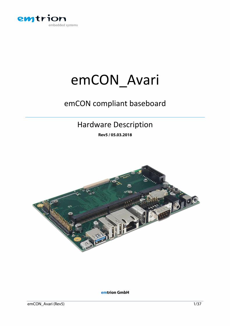
emCON_Avari
emCON compliant baseboard
Hardware Description Rev5 / 05.03.2018
emtrion GmbH
emCON_Avari (Rev5) 2/37
© Copyright 2018 emtrion GmbH
All rights reserved. This documentation may not be photocopied or recorded on any electronic
media without written approval. The information contained in this documentation is subject to
change without prior notice. We assume no liability for erroneous information or its consequences.
Trademarks used from other companies refer exclusively to the products of those companies.
Revision: 5 / 05.03.2018 Rev Date/Signature Changes
1 08.06.2015/Bue Initial release 2 24.10.2016/Bue Added CPU modules emCON-RZ/G1E and emCON-RZ/G1M,
reformatting of connector chapters 3 25.10.2016/Bue Signal LVDS1_BL-CTRL added at Pin 21 of J23 4 05.02.2018/Sch pin assignments corrections 5 05.03.2018/Bue Characteristics of CPU modules emCON-RZ/G1C and emCON-
RZ/G1H added
emCON_Avari (Rev5) 3/37
Table of Content
1 Introduction ................................................................................................................................................................ 5
2 Overview of emCON interfaces available at Avari ........................................................................................ 6
3 Connector Overview ................................................................................................................................................ 7
4 Handling Precautions .............................................................................................................................................. 7
5 Functional Description ........................................................................................................................................... 8
5.1 List of features ................................................................................................................................................... 8
6 General Features ....................................................................................................................................................... 9
6.1 Power Supply .................................................................................................................................................... 9
6.2 RTC Backup Battery, J21 ................................................................................................................................ 9
6.3 Board ID ............................................................................................................................................................... 9
6.4 CPU Boot Mode ............................................................................................................................................. 10
7 Connectors ............................................................................................................................................................... 11
7.1 emCON interface, J1 .................................................................................................................................... 11
7.2 DC Power Jack, J30 ....................................................................................................................................... 11
7.3 Ethernet ............................................................................................................................................................ 11
7.3.1 Ethernet Connector J16 .................................................................................................................... 12
7.4 USB Interfaces ................................................................................................................................................ 13
7.4.1 Overview ................................................................................................................................................ 13
7.4.2 USB 2.0 Host Interface ....................................................................................................................... 13
7.4.3 USB 2.0 Host Connector, J4, J5 ....................................................................................................... 13
7.4.4 USB 3.0 Host Interface ....................................................................................................................... 13
7.4.5 USB 3.0 Connector, J33 ..................................................................................................................... 14
7.4.6 USB 2.0 Host/Device ........................................................................................................................... 14
7.4.7 USB Host/Device Connector, J28 ................................................................................................... 15
7.5 miniPCIe ........................................................................................................................................................... 15
7.5.1 miniPCIe Socket, J17 .......................................................................................................................... 15
7.5.2 SIM Socket, J20 (not populated) .................................................................................................... 16
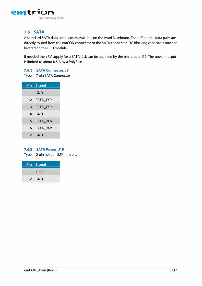
7.6 SATA .................................................................................................................................................................. 17
7.6.1 SATA Connector, J3 ............................................................................................................................ 17
7.6.2 SATA Power, J19 .................................................................................................................................. 17
7.7 Display Interfaces .......................................................................................................................................... 18
7.7.1 Overview ................................................................................................................................................ 18
7.7.2 RGB TFT Interface ................................................................................................................................ 18
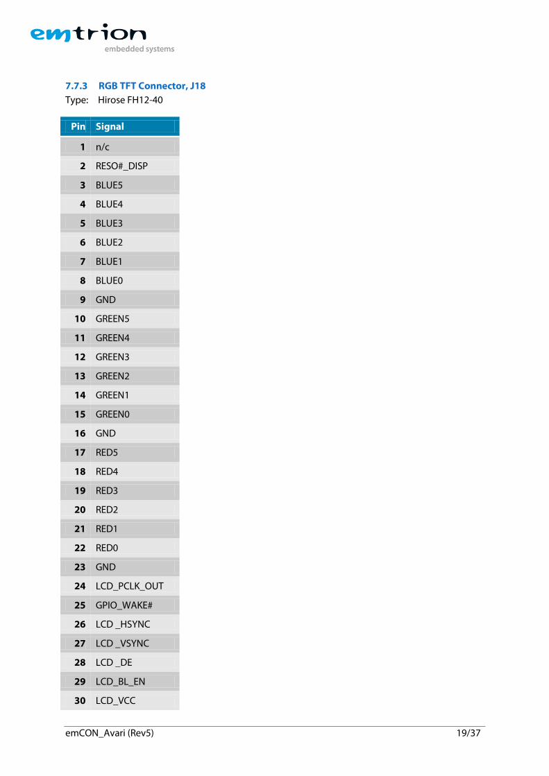
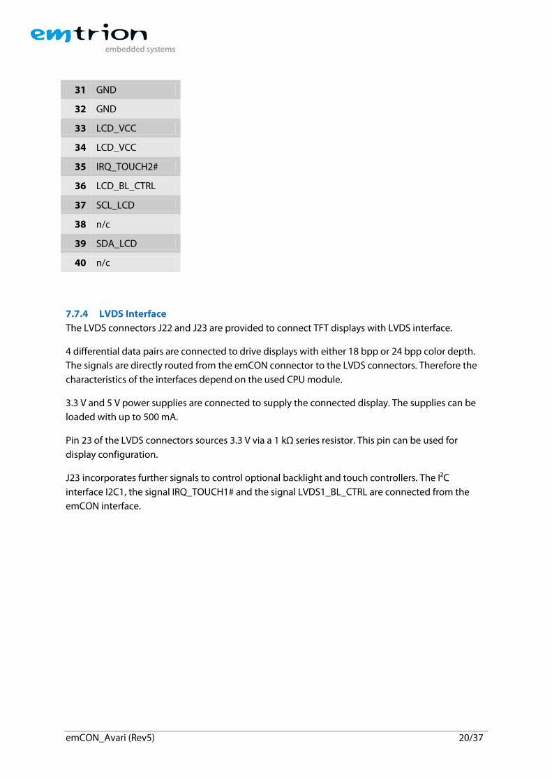
7.7.3 RGB TFT Connector, J18 .................................................................................................................... 19
7.7.4 LVDS Interface ...................................................................................................................................... 20
7.7.5 LVDS Connector, J22, J23 ................................................................................................................. 21
7.7.6 HDMI Interface ..................................................................................................................................... 22
7.7.7 HDMI Connector, J2 ............................................................................................................................ 22
7.8 Camera Interfaces ......................................................................................................................................... 23
7.8.1 Parallel Camera Interface .................................................................................................................. 23
7.8.2 Parallel Camera Connector, J7 ........................................................................................................ 23
7.8.3 MIPI CSI-2 Camera Interface ............................................................................................................ 23
7.8.4 MIPI CSI-2 Camera Connector, J9 .................................................................................................. 24
emCON_Avari (Rev5) 4/37
7.9 Headphone Out ............................................................................................................................................. 24
7.9.1 Audio Jack, J31 ..................................................................................................................................... 25
7.10 MicroSD Card Socket ................................................................................................................................... 25
7.10.1 microSD Card Socket, J8 ................................................................................................................... 25
7.11 CAN Interface ................................................................................................................................................. 26
7.11.1 CAN connector, J24 ............................................................................................................................ 26
7.12 UART Interfaces ............................................................................................................................................. 26
7.12.1 Overview ................................................................................................................................................ 26
7.12.2 UART A .................................................................................................................................................... 26
7.12.3 UART-A, J26 ........................................................................................................................................... 26
7.12.4 UART-B…UART-E ................................................................................................................................. 27
7.12.5 LVTTL UART connectors, J28, J29 .................................................................................................. 27
7.12.6 Availability of UART Interfaces ....................................................................................................... 28
7.13 Extension Connector ................................................................................................................................... 29
7.13.1 Extension Connector, J27 ................................................................................................................. 29
7.14 JTAG Connector ............................................................................................................................................. 30
7.14.1 JTAG Connector, J11 .......................................................................................................................... 30
7.15 Fan Connector ................................................................................................................................................ 30
7.15.1 Fan Connector, J13 ............................................................................................................................. 30
8 Buttons ...................................................................................................................................................................... 31
8.1 Reset Button S1.............................................................................................................................................. 31
8.2 WAKE, ON Button, S2, S3 ............................................................................................................................ 31
9 Board Dimensions ................................................................................................................................................. 32
10 emCON connector, J1 .......................................................................................................................................... 33
11 Technical Characteristics .................................................................................................................................... 37
11.1 Electrical Specifications .............................................................................................................................. 37
11.2 Environmental Specifications ................................................................................................................... 37
11.3 Mechanical Specifications ......................................................................................................................... 37
11.4 RoHS Compliance ......................................................................................................................................... 37
emCON_Avari (Rev5) 5/37
1 Introduction emCON_Avari (hereafter simply named Avari) is a carrier board for CPU modules of emtrion’s
emCON family. The Avari is intended to be used as a development platform that demonstrates the
capabilities of the emtrion CPU core modules. But it can also be used in series products.
A couple of interfaces of the CPU modules are available for customers at either standard
connectors or 2.54 mm pitch headers. Within them are high speed interfaces such as PCI Express,
SATA, USB 3.0, HDMI, GB Ethernet and LVDS. Additionally low speed multimedia interfaces like
RGB-LCD, Camera, Audio, SDC and industrial interfaces like CAN, UART, I2C, SPI and GPIOs are
available.
This manual describes the physical and electrical characteristics of the Avari board. It also covers
the use of it with different CPU Core modules if special things have to be observed. Since not all
CPU modules incorporate all interfaces of Avari it is recommended to read also the manual of the
CPU Core module that shall be used.
emCON_Avari (Rev5) 6/37
2 Overview of emCON interfaces available at Avari Avari Feature
X GB Ethernet 1 GB Ethernet 2
X SDC1 SDC2
X USB 3.0 Host
2 USB 2.0 Host X USB OTG X SATA
Headphone Out I2S Audio SPDIF
X HDMI X LVDS 1 X LVDS 2 X I2C1 I2C2
X Camera 1, Parallel Interface
X Camera 2, Serial Interface
X SPI1, QSPI X SPI2
18 Bit LCD-RGB 8 GPIO
miniPCIe PCIe Lane 1 PCIe Lane 2
PCIe Lane 3 PCIe Lane 4
RS232 UART-A X UART-B X UART-C X UART-D X UART-E X JTAG X Fan Connector 2 Touch IRQ X Power Management X 3.0 V Battery
X ON button X WAKE button X RESET button X CPU Boot
Configuration
emCON_Avari (Rev5) 7/37
3 Connector Overview
picture is missing
4 Handling Precautions Please read the following notes prior to installing CPU module to the Avari board. They apply to all
ESD (electrostatic discharge) sensitive components:
Before touching the board it is recommended that you discharge yourself by touching a
grounded object.
Be sure all tools required for installation are electrostatic discharged as well.
Before installing (or removing) a CPU module, unplug the power cable from your mains
supply.
Also switch off the power supply before you plug or unplug cables at connectors that not
ESD protected.
Handle the board with care and try to avoid touching its components or tracks.
emCON_Avari (Rev5) 8/37
5 Functional Description
5.1 List of features
The Avari provides the following interfaces and features.:
10/100/1000 Base-T Ethernet interface at RJ45 jack
USB 3.0 Host interface at USB-A socket
2 x USB 2.0 Host interface at USB-A socket
USB 2.0 OTG interface at MINI A/B socket
miniPCIe socket for Plugging Half-Mini and Full-Mini Modules with optional SIM Card
Holder *1
SATA
HDMI
2 x LVDS interface *2
18 bit RGB interface for EDT TFT displays with integrated capacitive touch controller
MIPI CSI-2, serial camera interface (2 lanes)
MIPI CPI, parallel camera interface *1
Stereo audio output with 58 mW @ 16 Ω at 3.5mm audio jack
Micro SD-Card socket
2 x CAN interface with TTL level at 10-pin header for adapter HiCO.ADA-CAN1
RS232 serial interface with flow control RTS/CTS at DSub-9 connector
LVTTL serial interface with flow control RTS/CTS at pin header for adapter HiCO.ADA232
3 x LVTTL serial interface without flow control at pin header for adapter HiCO.ADA232
30 pin extension connector with the following signals:
o 2 x SPI
o I²C
o 8 x GPIO from emCON connector
o External reset input
5 V PWM controlled output for fan at 4-pin header
Reset switch
ON button for power management
WAKE button for power management
3-bit CPU boot mode control by DIP switches
ARM compliant JTAG connector at 20-pin header
CR1632 battery holder for RTC backup
5 V Power jack with 2 mm pin
*1 This option is not fitted in the standard variant. Please ask emtrion for further Information
*2 The second interface not fitted in the standard variant. Please ask emtrion for further Information
emCON_Avari (Rev5) 9/37
6 General Features
6.1 Power Supply
The Avari base board must be supplied with +5 VDC, +/- 10%. The voltage is protected from
reverse polarity and overvoltage and directly connected to the pin VCC_STANDBY of the emCON
interface.
While the signal SUSPEND# of the emCON interface is driven higher than 3.0 V the 5 V supply is
switched to the power pins of the emCON connector and supplies the VBUS switches of the USB
Host interfaces.
A 3.3 VDC switching regulator with up to 6 A output current is populated on the Avari to supply the
local logic and interfaces of the board. This supply is enabled by driving the signal
POWER_ON_BASE of the emCON interface high. The signal is set to a high level by an on board
resistor while it is not driven by the CPU module. A green LED lights when the 3.3 V supply is on.
Important note:
The maximum power consumption of the whole system must not exceed 25W!
Please make sure that the Avari with plugged CPU module and connected devices like display,
USB devices, plugged PCIe board etc. do not exceed this limit! Otherwise the system might be
damaged.
6.2 RTC Backup Battery, J21
A battery holder J21 for a Lithium coin cell CR1632 is provided to supply the RTC of a plugged CPU
module. The battery voltage is available at the pin BAT of the emCON interface.
A 1 kΩ series resistor protects the battery from excessive current flow.
6.3 Board ID A plugged CPU module can read the Avari’s board ID code via the I²C interface I2C1 at the 7-bit
address 0x3A.
The board ID of the revision Avari-2 is 0x01.
emCON_Avari (Rev5) 10/37
6.4 CPU Boot Mode
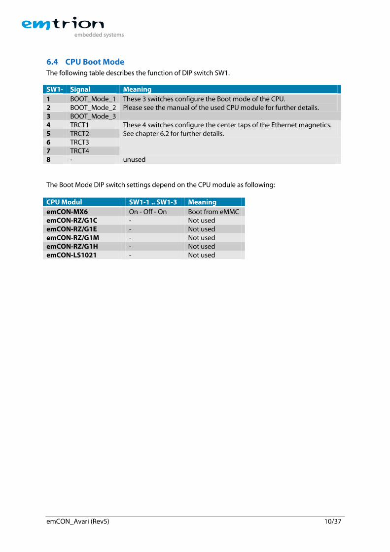
The following table describes the function of DIP switch SW1.
SW1- Signal Meaning
1 BOOT_Mode_1 These 3 switches configure the Boot mode of the CPU. Please see the manual of the used CPU module for further details. 2 BOOT_Mode_2
3 BOOT_Mode_3 4 TRCT1 These 4 switches configure the center taps of the Ethernet magnetics.
See chapter 6.2 for further details. 5 TRCT2 6 TRCT3 7 TRCT4 8 - unused
The Boot Mode DIP switch settings depend on the CPU module as following: CPU Modul SW1-1 .. SW1-3 Meaning
emCON-MX6 On - Off - On Boot from eMMC emCON-RZ/G1C - Not used emCON-RZ/G1E - Not used emCON-RZ/G1M - Not used emCON-RZ/G1H - Not used emCON-LS1021 - Not used
emCON_Avari (Rev5) 11/37
7 Connectors
7.1 emCON interface, J1
Type: MXM3 314 pin socket
emCON is an emtrion specific interface between emCON CPU modules and carrier boards. The
interface consists of a 314 pin SODIMM connector which is commonly used for MXM 3 graphic
modules.
All peripheral functions of the CPU modules are available at this connection. Also power is supplied
via the emCON interface.
Mechanical characteristics and a general pinout specification are described later in this document.
Watch: The pin assignment is specific for the emtrion boards and must not be used for other boards.
7.2 DC Power Jack, J30
Type: PJ_047AH
Pin Signal
Center Pin +5 V Outer Ring GND
7.3 Ethernet An RJ45 jack with integrated magnetics is provided for 10/100/1000 Mbit Ethernet.
To adapt the Ethernet interface to different PHYs on the CPU modules the center taps of the
magnetics can either be connected to a DC voltage sourced by pin GBE1_VCC of the emCON
connector or are AC coupled to GND by 100 nF capacitors. This is done by 4 DIP switches SW1-4 …
SW1-7. If a switch is closed the DC voltage is connected.
Watch:
The 4 DIP switches SW1-4 … SW1-7 must always have the same position. The DIP switch settings depend on the CPU module as following: CPU Modul SW1-4 .. SW1-7 Meaning
emCON-MX6 Off - Off - Off - Off AC coupled center taps emCON-RZ/G1C On - On - On - On center taps at GBE1_VCC emCON-RZ/G1E Off - Off - Off - Off AC coupled center taps emCON-RZ/G1M Off - Off - Off - Off AC coupled center taps emCON-RZ/G1M Off - Off - Off - Off AC coupled center taps emCON-LS1021 - -
emCON_Avari (Rev5) 12/37
Three LEDs inside the RJ45 jack can show the Link status, speed and traffic of the Ethernet interface.
The signaling depends on the CPU module as following:
CPU Modul Link/Speed Traffic
emCON-MX6 yellow on yellow blinking emCON-RZ/G1C yellow on yellow blinking emCON-RZ/G1E yellow on yellow blinking emCON-RZ/G1M yellow on yellow blinking emCON-RZ/G1H yellow on yellow blinking emCON-LS1021 - -
7.3.1 Ethernet Connector J16
Type: Rj45 Jack with magnetics (21 pin)
Pin Signal
1 TRCT3
2 TRD3_N
3 TRD3_P
4 TRD2_P
5 TRD2_N
6 TRCT2
7 TRCT4
8 TRD4_P
9 TRD4_N
10 TRD1_N
11 TRD1_P
12 TRCT1
13 LED1_K
14 3.3 V
15 LED2_K
16 3.3 V
17 LED3_K
emCON_Avari (Rev5) 13/37
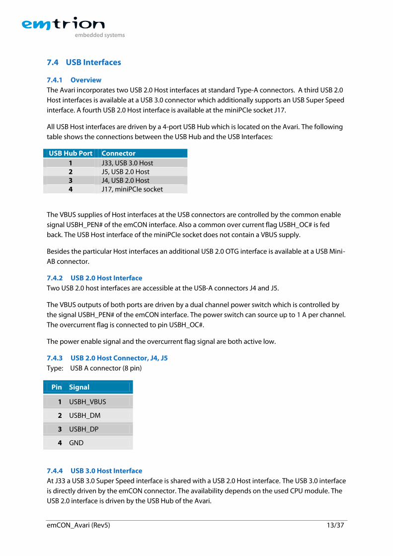
7.4 USB Interfaces
7.4.1 Overview
The Avari incorporates two USB 2.0 Host interfaces at standard Type-A connectors. A third USB 2.0
Host interfaces is available at a USB 3.0 connector which additionally supports an USB Super Speed
interface. A fourth USB 2.0 Host interface is available at the miniPCIe socket J17.
All USB Host interfaces are driven by a 4-port USB Hub which is located on the Avari. The following
table shows the connections between the USB Hub and the USB Interfaces:
USB Hub Port Connector
1 J33, USB 3.0 Host 2 J5, USB 2.0 Host 3 J4, USB 2.0 Host 4 J17, miniPCIe socket
The VBUS supplies of Host interfaces at the USB connectors are controlled by the common enable
signal USBH_PEN# of the emCON interface. Also a common over current flag USBH_OC# is fed
back. The USB Host interface of the miniPCIe socket does not contain a VBUS supply.
Besides the particular Host interfaces an additional USB 2.0 OTG interface is available at a USB Mini-
AB connector.
7.4.2 USB 2.0 Host Interface
Two USB 2.0 host interfaces are accessible at the USB-A connectors J4 and J5.
The VBUS outputs of both ports are driven by a dual channel power switch which is controlled by
the signal USBH_PEN# of the emCON interface. The power switch can source up to 1 A per channel.
The overcurrent flag is connected to pin USBH_OC#.
The power enable signal and the overcurrent flag signal are both active low.
7.4.3 USB 2.0 Host Connector, J4, J5
Type: USB A connector (8 pin)
Pin Signal
1 USBH_VBUS
2 USBH_DM
3 USBH_DP
4 GND
7.4.4 USB 3.0 Host Interface
At J33 a USB 3.0 Super Speed interface is shared with a USB 2.0 Host interface. The USB 3.0 interface
is directly driven by the emCON connector. The availability depends on the used CPU module. The
USB 2.0 interface is driven by the USB Hub of the Avari.
emCON_Avari (Rev5) 14/37
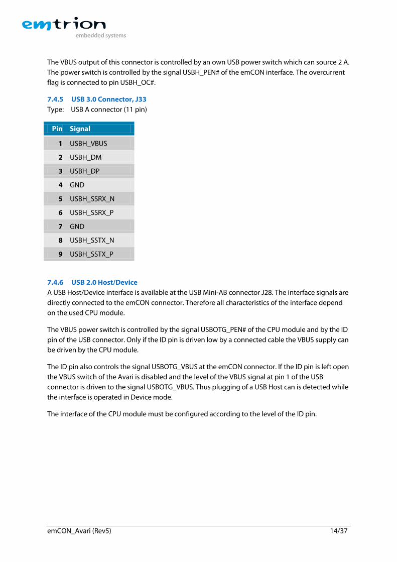
The VBUS output of this connector is controlled by an own USB power switch which can source 2 A.
The power switch is controlled by the signal USBH_PEN# of the emCON interface. The overcurrent
flag is connected to pin USBH_OC#.
7.4.5 USB 3.0 Connector, J33
Type: USB A connector (11 pin)
Pin Signal
1 USBH_VBUS
2 USBH_DM
3 USBH_DP
4 GND
5 USBH_SSRX_N
6 USBH_SSRX_P
7 GND
8 USBH_SSTX_N
9 USBH_SSTX_P
7.4.6 USB 2.0 Host/Device
A USB Host/Device interface is available at the USB Mini-AB connector J28. The interface signals are
directly connected to the emCON connector. Therefore all characteristics of the interface depend
on the used CPU module.
The VBUS power switch is controlled by the signal USBOTG_PEN# of the CPU module and by the ID
pin of the USB connector. Only if the ID pin is driven low by a connected cable the VBUS supply can
be driven by the CPU module.
The ID pin also controls the signal USBOTG_VBUS at the emCON connector. If the ID pin is left open
the VBUS switch of the Avari is disabled and the level of the VBUS signal at pin 1 of the USB
connector is driven to the signal USBOTG_VBUS. Thus plugging of a USB Host can is detected while
the interface is operated in Device mode.
The interface of the CPU module must be configured according to the level of the ID pin.
emCON_Avari (Rev5) 15/37
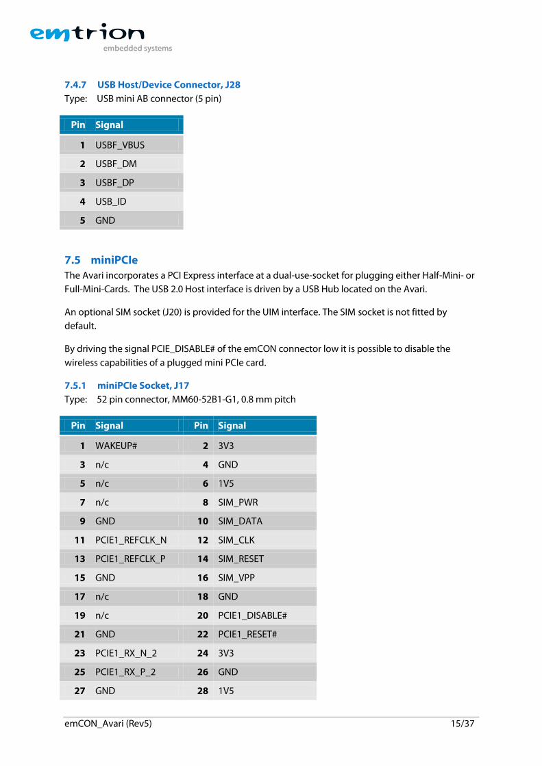
7.4.7 USB Host/Device Connector, J28
Type: USB mini AB connector (5 pin)
Pin Signal
1 USBF_VBUS
2 USBF_DM
3 USBF_DP
4 USB_ID
5 GND
7.5 miniPCIe
The Avari incorporates a PCI Express interface at a dual-use-socket for plugging either Half-Mini- or
Full-Mini-Cards. The USB 2.0 Host interface is driven by a USB Hub located on the Avari.
An optional SIM socket (J20) is provided for the UIM interface. The SIM socket is not fitted by
default.
By driving the signal PCIE_DISABLE# of the emCON connector low it is possible to disable the
wireless capabilities of a plugged mini PCIe card.
7.5.1 miniPCIe Socket, J17
Type: 52 pin connector, MM60-52B1-G1, 0.8 mm pitch
Pin Signal Pin Signal
1 WAKEUP# 2 3V3
3 n/c 4 GND
5 n/c 6 1V5
7 n/c 8 SIM_PWR
9 GND 10 SIM_DATA
11 PCIE1_REFCLK_N 12 SIM_CLK
13 PCIE1_REFCLK_P 14 SIM_RESET
15 GND 16 SIM_VPP
17 n/c 18 GND
19 n/c 20 PCIE1_DISABLE#
21 GND 22 PCIE1_RESET#
23 PCIE1_RX_N_2 24 3V3
25 PCIE1_RX_P_2 26 GND
27 GND 28 1V5
emCON_Avari (Rev5) 16/37
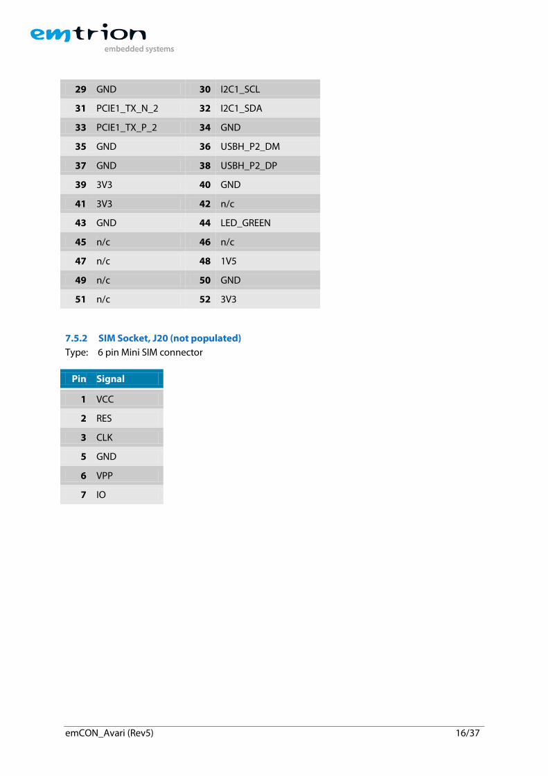
29 GND 30 I2C1_SCL
31 PCIE1_TX_N_2 32 I2C1_SDA
33 PCIE1_TX_P_2 34 GND
35 GND 36 USBH_P2_DM
37 GND 38 USBH_P2_DP
39 3V3 40 GND
41 3V3 42 n/c
43 GND 44 LED_GREEN
45 n/c 46 n/c
47 n/c 48 1V5
49 n/c 50 GND
51 n/c 52 3V3
7.5.2 SIM Socket, J20 (not populated)
Type: 6 pin Mini SIM connector
Pin Signal
1 VCC
2 RES
3 CLK
5 GND
6 VPP
7 IO
emCON_Avari (Rev5) 17/37
7.6 SATA
A standard SATA data connector is available on the Avari Baseboard. The differential data pairs are
directly routed from the emCON connector to the SATA connector. DC blocking capacitors must be
located on the CPU module.
If needed the +5V supply for a SATA disk can be supplied by the pin header J19. The power output
is limited to about 0.5 A by a Polyfuse.
7.6.1 SATA Connector, J3
Type: 7 pin SATA Connector
Pin Signal
1 GND
2 SATA_TXP
3 SATA_TXP
4 GND
5 SATA_RXN
6 SATA_RXP
7 GND
7.6.2 SATA Power, J19
Type: 2 pin header, 2.54 mm pitch
Pin Signal
1 + 5V
2 GND
emCON_Avari (Rev5) 18/37
7.7 Display Interfaces
7.7.1 Overview
The Avari provides connectors for different display types.
- The connector J18 is provided to connect a TFT display with 18-bit RGB interface. The
connector conforms to the special display family from the company EDT.
- The connectors J22 and J23 are used to connect TFT displays with LVDS interface.
- The connector J2 is a standard connector for displays with HDMI interface.
All display interfaces are directly driven by the CPU module via the emCON connector. The use of
the other interfaces depends on the plugged CPU module.
7.7.2 RGB TFT Interface
A TFT LCD display with 18 bpp color resolution can be connected to the connector J18. The pinout
of the connector conforms to a family of TFT displays that is available from the company EDT.
Besides that other TFT displays can also be connected with an appropriate adapter.
In principal these displays are offered either with integrated 4-wire resistive touch interface or with
projected capacitive touch interface. The connector J18 is realized only for displays with capacitive
touch interface. In this case a capacitive touch controller is located on the back side of the display.
The touch controller is connected to the I²C interface I2C1 of the emCON interface. The touch
controller’s wake input is driven by GPIO_4. The touch controller’s interrupt output is connected to
the signal IRQ_TOUCH2#. Further details about the touch controller can be found in the displays
data sheet.
The backlight of the display is enabled by the signal LCD_BL_EN of the emCON interface.
Additionally the brightness can be controlled by the signal LCD_BL_CTRL. This signal should be
driven by a PWM output.
The 3.3 V power supply of a display which is connected to J18 can be switched on and off by the
signal LCD_PANEL_EN from the emCON connector. The power supply is enabled while the signal is
high.
Since different displays use different pixel clock slopes to latch the data the active clock slope can
be configured by solder bridges at J32. By default the pixel clock signal is inverted. If needed please
ask emtrion for further information.
emCON_Avari (Rev5) 19/37
7.7.3 RGB TFT Connector, J18
Type: Hirose FH12-40
Pin Signal
1 n/c
2 RESO#_DISP
3 BLUE5
4 BLUE4
5 BLUE3
6 BLUE2
7 BLUE1
8 BLUE0
9 GND
10 GREEN5
11 GREEN4
12 GREEN3
13 GREEN2
14 GREEN1
15 GREEN0
16 GND
17 RED5
18 RED4
19 RED3
20 RED2
21 RED1
22 RED0
23 GND
24 LCD_PCLK_OUT
25 GPIO_WAKE#
26 LCD _HSYNC
27 LCD _VSYNC
28 LCD _DE
29 LCD_BL_EN
30 LCD_VCC
emCON_Avari (Rev5) 20/37
31 GND
32 GND
33 LCD_VCC
34 LCD_VCC
35 IRQ_TOUCH2#
36 LCD_BL_CTRL
37 SCL_LCD
38 n/c
39 SDA_LCD
40 n/c
7.7.4 LVDS Interface
The LVDS connectors J22 and J23 are provided to connect TFT displays with LVDS interface.
4 differential data pairs are connected to drive displays with either 18 bpp or 24 bpp color depth.
The signals are directly routed from the emCON connector to the LVDS connectors. Therefore the
characteristics of the interfaces depend on the used CPU module.
3.3 V and 5 V power supplies are connected to supply the connected display. The supplies can be
loaded with up to 500 mA.
Pin 23 of the LVDS connectors sources 3.3 V via a 1 kΩ series resistor. This pin can be used for
display configuration.
J23 incorporates further signals to control optional backlight and touch controllers. The I²C
interface I2C1, the signal IRQ_TOUCH1# and the signal LVDS1_BL_CTRL are connected from the
emCON interface.
emCON_Avari (Rev5) 21/37
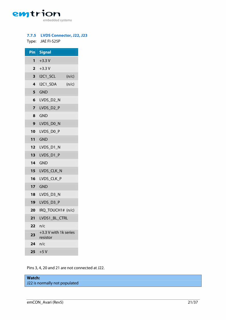
7.7.5 LVDS Connector, J22, J23
Type: JAE FI-S25P
Pin Signal
1 +3.3 V
2 +3.3 V
3 I2C1_SCL (n/c)
4 I2C1_SDA (n/c)
5 GND
6 LVDS_D2_N
7 LVDS_D2_P
8 GND
9 LVDS_D0_N
10 LVDS_D0_P
11 GND
12 LVDS_D1_N
13 LVDS_D1_P
14 GND
15 LVDS_CLK_N
16 LVDS_CLK_P
17 GND
18 LVDS_D3_N
19 LVDS_D3_P
20 IRQ_TOUCH1# (n/c)
21 LVDS1_BL_CTRL
22 n/c
23 +3.3 V with 1k series resistor
24 n/c
25 +5 V
Pins 3, 4, 20 and 21 are not connected at J22.
Watch: J22 is normally not populated

emCON_Avari (Rev5) 22/37
7.7.6 HDMI Interface
A standard monitor with HDMI interface can be connected at connector J2. The HDMI signals of the
emCON connector are directly routed to it.
The I²C interface for display identification (DDC) and the hot plug signal are also connected to the
emCON pins.
7.7.7 HDMI Connector, J2
Type: HDMI
Pin Signal
1 HDMI_D2_P
2 GND
3 HDMI_D2_N
4 HDMI_D1_P
5 GND
6 HDMI_D1_N
7 HDMI_D0_P
8 GND
9 HDMI_D0_N
10 HDMI_CLK_P
11 GND
12 HDMI_CLK_N
13 CEC_OUT
14 n/c
15 I2C1_SCL_5V
16 I2C1_SDA_5V
17 GND
18 5V
19 HPD_OUT
emCON_Avari (Rev5) 23/37
7.8 Camera Interfaces
7.8.1 Parallel Camera Interface
The interface CR1 of the emCON connector is specified to connect a CMOS camera sensor with 8 bit
data bus, pixel clock, HSYNC and VSYNC. These signals are routed to the 26 pos pin header J7.
Besides the camera data interface the I²C interface I2C1 and 3.3 V and 5 V supplies are available at
connector J7.
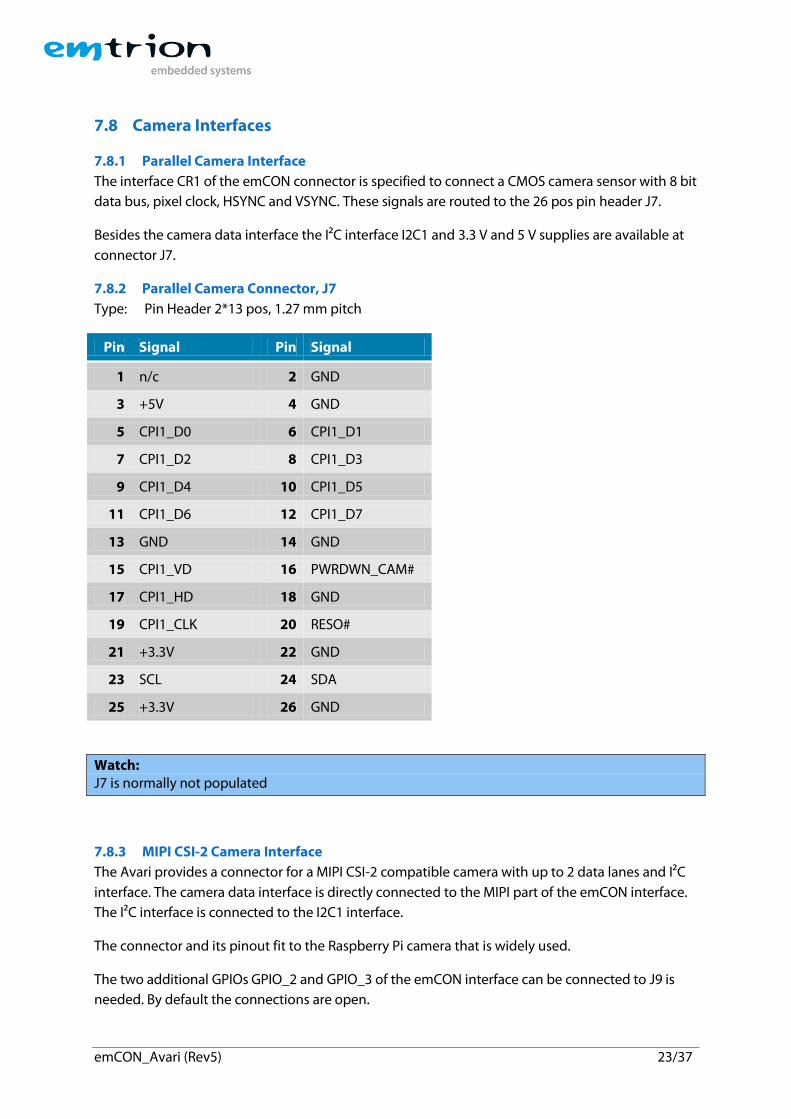
7.8.2 Parallel Camera Connector, J7
Type: Pin Header 2*13 pos, 1.27 mm pitch
Pin Signal Pin Signal
1 n/c 2 GND
3 +5V 4 GND
5 CPI1_D0 6 CPI1_D1
7 CPI1_D2 8 CPI1_D3
9 CPI1_D4 10 CPI1_D5
11 CPI1_D6 12 CPI1_D7
13 GND 14 GND
15 CPI1_VD 16 PWRDWN_CAM#
17 CPI1_HD 18 GND
19 CPI1_CLK 20 RESO#
21 +3.3V 22 GND
23 SCL 24 SDA
25 +3.3V 26 GND
Watch: J7 is normally not populated
7.8.3 MIPI CSI-2 Camera Interface
The Avari provides a connector for a MIPI CSI-2 compatible camera with up to 2 data lanes and I²C
interface. The camera data interface is directly connected to the MIPI part of the emCON interface.
The I²C interface is connected to the I2C1 interface.
The connector and its pinout fit to the Raspberry Pi camera that is widely used.
The two additional GPIOs GPIO_2 and GPIO_3 of the emCON interface can be connected to J9 is
needed. By default the connections are open.
emCON_Avari (Rev5) 24/37
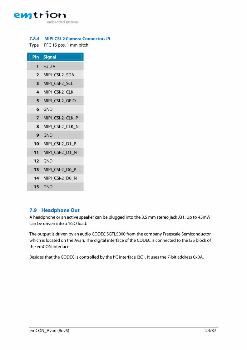
7.8.4 MIPI CSI-2 Camera Connector, J9
Type FFC 15 pos, 1 mm pitch
Pin Signal
1 +3.3 V
2 MIPI_CSI-2_SDA
3 MIPI_CSI-2_SCL
4 MIPI_CSI-2_CLK
5 MIPI_CSI-2_GPIO
6 GND
7 MIPI_CSI-2_CLK_P
8 MIPI_CSI-2_CLK_N
9 GND
10 MIPI_CSI-2_D1_P
11 MIPI_CSI-2_D1_N
12 GND
13 MIPI_CSI-2_D0_P
14 MIPI_CSI-2_D0_N
15 GND
7.9 Headphone Out
A headphone or an active speaker can be plugged into the 3.5 mm stereo jack J31. Up to 45mW
can be driven into a 16 Ω load.
The output is driven by an audio CODEC SGTL5000 from the company Freescale Semiconductor
which is located on the Avari. The digital interface of the CODEC is connected to the I2S block of
the emCON interface.
Besides that the CODEC is controlled by the I²C interface I2C1. It uses the 7-bit address 0x0A.
emCON_Avari (Rev5) 25/37
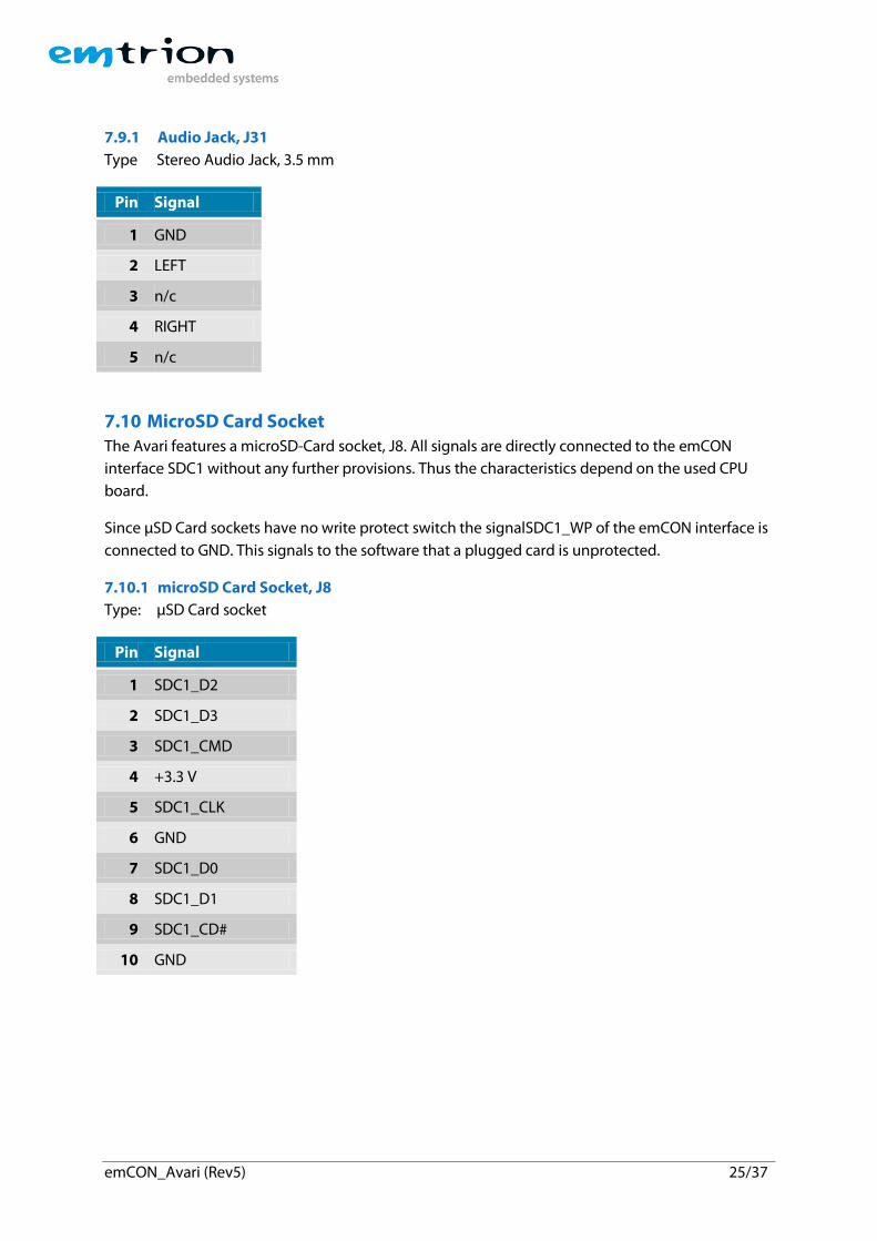
7.9.1 Audio Jack, J31
Type Stereo Audio Jack, 3.5 mm
Pin Signal
1 GND
2 LEFT
3 n/c
4 RIGHT
5 n/c
7.10 MicroSD Card Socket
The Avari features a microSD-Card socket, J8. All signals are directly connected to the emCON
interface SDC1 without any further provisions. Thus the characteristics depend on the used CPU
board.
Since µSD Card sockets have no write protect switch the signalSDC1_WP of the emCON interface is
connected to GND. This signals to the software that a plugged card is unprotected.
7.10.1 microSD Card Socket, J8
Type: µSD Card socket
Pin Signal
1 SDC1_D2
2 SDC1_D3
3 SDC1_CMD
4 +3.3 V
5 SDC1_CLK
6 GND
7 SDC1_D0
8 SDC1_D1
9 SDC1_CD#
10 GND
emCON_Avari (Rev5) 26/37
7.11 CAN Interface
Type Pin header 2*5 pos, 2.54 mm pitch
The transmit and receive signals of two CAN channels are connected from the emCON connector
to J24 as LVTTL signals. Additionally 3.3 V supply and GND are connected.
By plugging adapters ADA-CAN_3V3 from emtrion two CAN interfaces can be realized. Pin 1 of the
adapters must direct to the dots at J24.
7.11.1 CAN connector, J24
Type Pin header 2*5 pos, 2.54 mm pitch
Pin Signal Pin Signal
1 +3.3 V 2 +3.3 V
3 GND 4 GND
5 CAN2_TX 6 CAN2_TX
7 CAN2_RX 8 CAN2_RX
9 n/c 10 n/c
7.12 UART Interfaces
7.12.1 Overview
The Avari provides connectors for up to 5 UART interfaces. Interface UART A is realized as RS232
interface at a D-Sub 9 connector. The other four interfaces UART B…UART E are directly connected
as LVTTL signals from the emCON interface to pin headers. The detailed electrical characteristics of
the interfaces depend on the plugged CPU module.
7.12.2 UART A
UART interface A is available at a standard D-Sub 9 connector with RS232 compatible levels.
Besides the data lines RTS and CTS flow control signals are connected. The RS232 transceiver is
located on Avari.
7.12.3 UART-A, J26
Type: D-Sub-9, male
Pin Signal
1 n/c
2 UART_A_RXD#
3 UART_A_TXD#
4 n/c
5 GND
6 n/c
emCON_Avari (Rev5) 27/37
7 UART_A_RTS#
8 UART_A_CTS#
9 n/c
7.12.4 UART-B…UART-E
The interfaces UART-B and UART-C share the connector J28. They are connected directly as LVTTL
signals to the emCON connector.
The interfaces UART-D and UART-E share the connector J29. They are connected directly as LVTTL
signals to the emCON connector.
Only UART-B incorporates the flow control signals RTS and CTS. The other three interfaces consist
only of transmit and receive lines.
The pinout of the connectors J28 and J29 fits to the adapter ADA_RS232 from emtrion which
contains an RS232 transceiver and drives the signals to a D-Sub 9 connector.
7.12.5 LVTTL UART connectors, J28, J29
Type Pin header 2*6, 2.54 mm pitch
Pin Signal Pin Signal
1 +3.3V 2 +3.3V
3 GND 4 GND
5 UART_TXD 6 UART_TXD
7 UART_RXD 8 UART_RXD
9 (UART_RTS) 10 n/c
11 (UART_CTS) 12 n/c
Signals UART_RTS and UART_CTS are not connected at J29.
emCON_Avari (Rev5) 28/37
7.12.6 Availability of UART Interfaces
The availability of the UART interfaces depends on the plugged CPU module as following:
emCON-MX6x:
Port Flow Control CPU-Interface Level
UART_A RTS, CTS UART2 RS232 transceiver on Avari UART_B - UART1 LVTTL UART_C - UART3 LVTTL UART_D - UART4 LVTTL UART_E - UART5 LVTTL
emCON-RZ/G1C:
Port Flow Control CPU-Interface Level
UART_A RTS, CTS HSCIF1 RS232 transceiver on Avari UART_B RTS, CTS HSCIF2 LVTTL UART_C - SCIF3 LVTTL UART_D - SCIF4 LVTTL UART_E - SCIF5 LVTTL
emCON-RZ/G1E:
Port Flow Control CPU-Interface Level
UART_A RTS, CTS HSCIF2 RS232 transceiver on Avari UART_B - - - UART_C - SCIF5 LVTTL UART_D - SCIF4 LVTTL UART_E - -
emCON-RZ/G1M:
Port Flow Control CPU-Interface Level
UART_A RTS, CTS HSCIF0 RS232 transceiver on Avari UART_B RTS, CTS HSCIF1 LVTTL UART_C - SCIF2 LVTTL UART_D - SCIF3 LVTTL UART_E - SCIF4 LVTTL
emCON-RZ/G1H:
Port Flow Control CPU-Interface Level
UART_A RTS, CTS SCIFA1 RS232 transceiver on Avari UART_B RTS, CTS SCIFB2 LVTTL UART_C - HSCIF1 LVTTL UART_D - SCIFA2 LVTTL UART_E - SCIFA0 LVTTL
emCON_Avari (Rev5) 29/37
7.13 Extension Connector
The pin header J27 features 8 * GPIO, 2 * SPI interface, an I²C-Bus interface, an active low reset
input signal RESI_EXT# and an active low reset output signal RESET#.
The GPIO pins GPIO_[8:1] and the SPI interface SPI1 and SPI2 are directly connected from the
emCON connector.
The I²C interface I2C1 at J27 is decoupled from the emCON connector by a bidirectional repeater
circuit without level translation. The output high level is 3.3 V.
7.13.1 Extension Connector, J27
Type: Pin Header 2*15, 2.54 mm pitch
Pin Signal Pin Signal
1 GND 2 +3.3 V
3 SPI1_SS# 4 SPI1_CS1/D2
5 SPI1_SCK 6 SPI1_D3
7 SPI1_MISO/D1 8 GPIO_1
9 SPI1_MOSI /D0 10 GPIO_2
11 GND 12 GPIO_3
13 SPI2_CS0# 14 GPIO_4
15 SPI2_SCK 16 GPIO_5
17 SPI2_MISO 18 GPIO_6
19 SPI2_MOSI 20 GPIO_7
21 GND 22 GPIO_8
23 SCL1 24 RESO#
25 SDA1 26 RESI#
27 GND 28 +3.3 V
29 SPI2_CS1# 30 +3.3 V
emCON_Avari (Rev5) 30/37
7.14 JTAG Connector
For debugging emCON CPU modules the JTAG signals are provided at the emCON connector and
routed to the shrouded pin header J11. The pinout of J11 conforms to the ARM JTAG specification.
7.14.1 JTAG Connector, J11
Type Shrouded pin header 2*10, 2.54 mm pitch
Pin Signal Pin Signal
1 JTAG_VCC 2 JTAG_VCC
3 GND 4 JTAG_TRST
5 GND 6 JTAG_TDI
7 GND 8 JTAG_TMS
9 GND 10 JTAG_TCK
11 GND 12 JTAG_RTCK
13 GND 14 JTAG_TDO
15 GND 16 JTAG_RESET#
17 GND 18 n/c
19 GND 20 n/c
7.15 Fan Connector A connector is provided which can be used to supply a fan with 5 VDC. By a low side switch which
is controlled by the PWM signal PWM_FAN of the emCON connector the fan speed can be
controlled.
The 5 V output is protected by a resettable fuse with 0.5 A.
7.15.1 Fan Connector, J13
Type Pin header 1*4, 2.54 mm pitch
Pin Signal
1 GND
2 +5V
3 n/c
4 PWM_FAN_5V#
emCON_Avari (Rev5) 31/37
8 Buttons
8.1 Reset Button S1
Pressing the button S1 of the Avari causes immediately the signal POWERFAIL# of the emCON
interface to become low. Pressing the button longer than 4 s additionally causes the signal RESI# of
the emCON interface to become low.
The signal RESI_EXT# at connector J27 has the same behavior as the button S1.
8.2 WAKE, ON Button, S2, S3 Two push buttons marked as WAKE and ON are provided for power management features. While
pressed these keys drive the appropriate signals WAKEUP# and ON_OFF# of the emCON interface
low.
The use of these buttons depends on the plugged CPU module.
emCON_Avari (Rev5) 32/37
9 Board Dimensions
J1
J16
J17
J32
J21
J6 J26
J22
J19
J5J2
J23
J4
SW1
J33S1
J3
J30
J11J24
J27
J13
J34
J28J29
S2
S3
J31
6.00 mm
150.00 mm
17.5
0 m
m7.0
0 m
m
100.0
0 m
m
emCON_Avari (Rev5) 33/37
10 emCON connector, J1 Type 314 pin emCON socket, 0.5 mm Pitch
Pin Signal Interface Signal Pin
1E20 GND
Po
we
r
VCC 5V 2E20
1E19 GND VCC 5V 2E19
1E18 GND VCC 5V 2E18
1E17 GND VCC 5V 2E17
1E16 GND VCC 5V 2E16
1E15 GND VCC 5V 2E15
1E14 GND VCC 5V 2E14
1E13 GND VCC 5V 2E13
1E12 GND VCC 5V 2E12
1E11 GND VCC 5V 2E11
1E10 BAT VCC_STANDBY 2E10
1E09 BOOT_MODE_3
Ma
nu
fact
uri
ng
Mis
c TAMPER 2E09
1E08 BOOT_MODE_2 POWER_ON_BASE 2E08
1E07 BOOT_MODE_1 IRQ_TOUCH1# 2E07
1E06 JTAG_RESET# IRQ_TOUCH2# 2E06
1E05 JTAG_MOD n/c 2E05
1E04 JTAG_TRST# n/c 2E04
1E03 JTAG_TMS n/c 2E03
1E02 JTAG_TDO RESO# 2E02
1E01 JTAG_TDI RESI# 2E01
1 JTAG_RTCK POWERFAIL# 2
3 JTAG_VCC SUSPEND# 4
5 JTAG_TCK ON_OFF# 6
7 GND Power WAKEUP# 8
9 UART-A_RXD
UART-A
PWM_FAN 10
11 UART-A_TXD Power GND 12
13 UART-A_RTS UART-C
UART-C_RXD 14
15 UART-A_CTS UART-C_TXD 16
17 UART-B_RXD
UART-B
UART-D UART-D_RXD 18
19 UART-B_TXD UART-D_TXD 20
21 UART-B_RTS UART-E
UART-E_RXD 22
23 UART-B_CTS UART-E_TXD 24
25 GND Power GND 26
27 GPIO_1
GP
IO
PC
Ie1
PCIE_DISABLE# 28
29 GPIO_2 PCIE_RESET# 30
31 GPIO_3 PCIE_CLK1_P 32
33 GPIO_4 PCIE_CLK2_N 34
35 GPIO_5 GND 36
37 GPIO_6 PCIE_RX1_P 38
39 GPIO_7 PCIE_RX1_N 40
41 GPIO_8 PCIE_TX1_P 42
43 GND Power PCIE_TX1_N 44
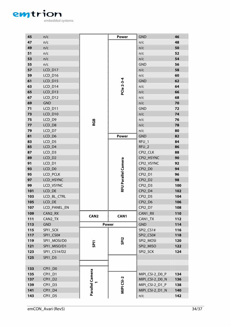
emCON_Avari (Rev5) 34/37
45 n/c
RG
B
Power GND 46
47 n/c
PC
Ie 2
-3-4
n/c 48
49 n/c n/c 50
51 n/c n/c 52
53 n/c n/c 54
55 n/c GND 56
57 LCD_D17 n/c 58
59 LCD_D16 n/c 60
61 LCD_D15 GND 62
63 LCD_D14 n/c 64
65 LCD_D13 n/c 66
67 LCD_D12 n/c 68
69 GND n/c 70
71 LCD_D11 GND 72
73 LCD_D10 n/c 74
75 LCD_D9 n/c 76
77 LCD_D8 n/c 78
79 LCD_D7 n/c 80
81 LCD_D6 Power GND 82
83 LCD_D5
RF
U P
ara
lle
l Ca
me
ra
RFU_1 84
85 LCD_D4 RFU_2 86
87 LCD_D3 CPI2_CLK 88
89 LCD_D2 CPI2_HSYNC 90
91 LCD_D1 CPI2_VSYNC 92
93 LCD_D0 CPI2_D0 94
95 LCD_PCLK CPI2_D1 96
97 LCD_HSYNC CPI2_D2 98
99 LCD_VSYNC CPI2_D3 100
101 LCD_DE CPI2_D4 102
103 LCD_BL_CTRL CPI2_D5 104
105 LCD_DE CPI2_D6 106
107 LCD_PANEL_EN CPI2_D7 108
109 CAN2_RX CAN2 CAN1
CAN1_RX 110
111 CAN2_TX CAN1_TX 112
113 GND Power GND 114
115 SPI1_SCK
SP
I1
SP
I2
SPI2_CS1# 116
117 SPI1_CS0# SPI2_CS0# 118
119 SPI1_MOSI/D0 SPI2_MOSI 120
121 SPI1_MISO/D1 SPI2_MISO 122
123 SPI1_CS1#/D2 SPI2_SCK 124
125 SPI1_D3
133 CPI1_D0
Pa
rall
el C
am
era
1
135 CPI1_D1
MIP
I CS
I-2
MIPI_CSI-2_D0_P 134
137 CPI1_D2 MIPI_CSI-2_D0_N 136
139 CPI1_D3 MIPI_CSI-2_D1_P 138
141 CPI1_D4 MIPI_CSI-2_D1_N 140
143 CPI1_D5 n/c 142
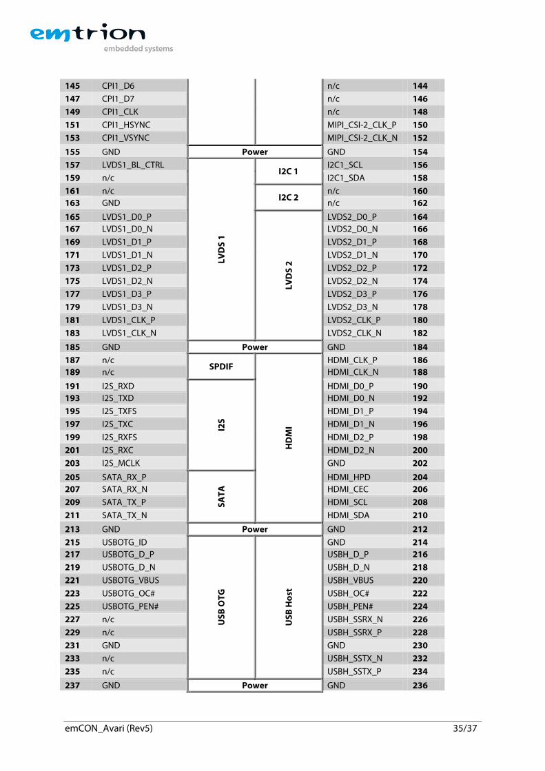
emCON_Avari (Rev5) 35/37
145 CPI1_D6 n/c 144
147 CPI1_D7 n/c 146
149 CPI1_CLK n/c 148
151 CPI1_HSYNC MIPI_CSI-2_CLK_P 150
153 CPI1_VSYNC MIPI_CSI-2_CLK_N 152
155 GND Power GND 154
157 LVDS1_BL_CTRL
LV
DS
1
I2C 1 I2C1_SCL 156
159 n/c I2C1_SDA 158
161 n/c I2C 2
n/c 160
163 GND n/c 162
165 LVDS1_D0_P
LV
DS
2
LVDS2_D0_P 164
167 LVDS1_D0_N LVDS2_D0_N 166
169 LVDS1_D1_P LVDS2_D1_P 168
171 LVDS1_D1_N LVDS2_D1_N 170
173 LVDS1_D2_P LVDS2_D2_P 172
175 LVDS1_D2_N LVDS2_D2_N 174
177 LVDS1_D3_P LVDS2_D3_P 176
179 LVDS1_D3_N LVDS2_D3_N 178
181 LVDS1_CLK_P LVDS2_CLK_P 180
183 LVDS1_CLK_N LVDS2_CLK_N 182
185 GND Power GND 184
187 n/c SPDIF
HD
MI
HDMI_CLK_P 186
189 n/c HDMI_CLK_N 188
191 I2S_RXD
I2S
HDMI_D0_P 190
193 I2S_TXD HDMI_D0_N 192
195 I2S_TXFS HDMI_D1_P 194
197 I2S_TXC HDMI_D1_N 196
199 I2S_RXFS HDMI_D2_P 198
201 I2S_RXC HDMI_D2_N 200
203 I2S_MCLK GND 202
205 SATA_RX_P
SA
TA
HDMI_HPD 204
207 SATA_RX_N HDMI_CEC 206
209 SATA_TX_P HDMI_SCL 208
211 SATA_TX_N HDMI_SDA 210
213 GND Power GND 212
215 USBOTG_ID
US
B O
TG
US
B H
ost
GND 214
217 USBOTG_D_P USBH_D_P 216
219 USBOTG_D_N USBH_D_N 218
221 USBOTG_VBUS USBH_VBUS 220
223 USBOTG_OC# USBH_OC# 222
225 USBOTG_PEN# USBH_PEN# 224
227 n/c USBH_SSRX_N 226
229 n/c USBH_SSRX_P 228
231 GND GND 230
233 n/c USBH_SSTX_N 232
235 n/c USBH_SSTX_P 234
237 GND Power GND 236
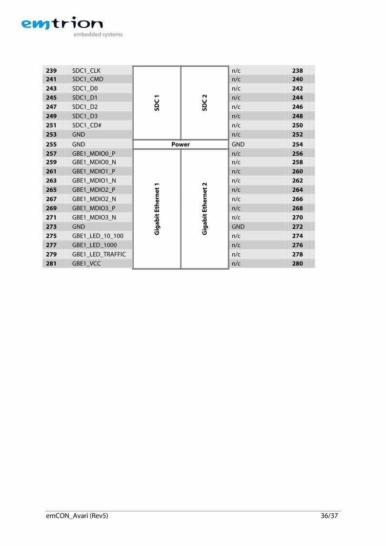
emCON_Avari (Rev5) 36/37
239 SDC1_CLK
SD
C 1
SD
C 2
n/c 238
241 SDC1_CMD n/c 240
243 SDC1_D0 n/c 242
245 SDC1_D1 n/c 244
247 SDC1_D2 n/c 246
249 SDC1_D3 n/c 248
251 SDC1_CD# n/c 250
253 GND n/c 252
255 GND Power GND 254
257 GBE1_MDIO0_P G
iga
bit
Eth
ern
et
1
Gig
ab
it E
the
rne
t 2
n/c 256
259 GBE1_MDIO0_N n/c 258
261 GBE1_MDIO1_P n/c 260
263 GBE1_MDIO1_N n/c 262
265 GBE1_MDIO2_P n/c 264
267 GBE1_MDIO2_N n/c 266
269 GBE1_MDIO3_P n/c 268
271 GBE1_MDIO3_N n/c 270
273 GND GND 272
275 GBE1_LED_10_100 n/c 274
277 GBE1_LED_1000 n/c 276
279 GBE1_LED_TRAFFIC n/c 278
281 GBE1_VCC n/c 280
emCON_Avari (Rev5) 37/37
11 Technical Characteristics
11.1 Electrical Specifications
Supply Voltage +5V, +/-10%
Current consumption 27 mA, (3.3 V enabled, nothing plugged)
11.2 Environmental Specifications
Operating Temperature -25°C ... +80°C
Storage temperature -40°C ... +125°C
Relative humidity 0 ... 95 %, non-condensing
11.3 Mechanical Specifications
Weight approx. 102 g
Board FR-4, UL94V-0, 8 layers
Dimensions 150 mm x 100 mm x 18 mm
11.4 RoHS Compliance Avari is RoHs compliant according to European Union’s Directive 2002/95/EC: "Restrictions of
Hazardous Substances".