Embed Size (px)
Citation preview
Ecole Navale
Et
Groupe des Ecoles du Poulmic
PROJET DE FIN D’ETUDES
GENIE ENERGETIQUE.
ANALYSIS AND DESIGN OF A FORWARD CONVERTER.
Promotion 2006
EV2 Arboy
EV2 Cousin
Universidade Federal de Santa Catarina. Instituto de Eletrônica de Potência

Acknowledgment
We would like to thank Professor Ivo Barbi for his help and his patience during the entire
Project. We would like also to thank the technicians who built our full circuit especially Mr.
Pacheco. We are also very grateful to Professor Marcelo for his help during the test phase of
our project. Finally we thank Professor Marion who help us in the correction of this report.

Analysis and design of a Forward Converter.
Students : EV2. C. Arboy et B. Cousin, EN 2006
Type of report : Rapport de Projet de Fin d’Etude (PFE)
University : Federal University of Santa Catarina (UFSC)
Power Electronic Engineering Department (INEP)
Project chief : Ivo Barbi, Professor in Power Electronics Institute at the UFSC
ABSTRACT
Our project consists in the study, the design and the realization of a Forward converter.
The design of a forward converter demands great precision when calculating the different
parameters and restrictions that will have to be applied when conceiving the model.
The first step was the understanding of the forward converter in order to know the main
parameters needed and the different mathematical equations for the choice of the different
components of the forward. The use of the software PSIM completes this work for the
comprehension,the collection of different values and for the checking of the circuit
calculations.
Once this had been done it was possible to proceed to the construction and to the test the
forward converter in the laboratory. These different tests allowed us to validate the performed
design and simulations.
Then we have controlled the output voltage of the forward converter with a feedback
control circuit in order to assure the optimal function of the forward and automatic control of
the different parameters.
RESUME
Ce projet a pour but l’étude et la réalisation complète d’un convertisseur Forward
s’inscrivant dans un cahier des charges bien précis afin d’être tester.
Un travail préliminaire portant sur l’étude qualitatives du convertisseur permet de dégager
les nombreux paramètres qu’il sera nécessaire de surveiller ainsi que d’obtenir les différentes
équations mathématiques utiles pour dimensionner les éléments constitutif du convertisseur.
La simulation par outil informatique vient compléter cette démarche amont et nous aide
ainsi à accéder à des résultats qu’il convient de confronter une fois le prototype réaliser.
Ensuite le convertisseur une fois dimensionner, en ayant respecté au maximum le cahier
des charges est construit puis testé. Ces différents tests nous permettent de valider notre
convertisseur et les simulations effectuées.
Enfin l’intégration dans une chaine de contrôle permet d’asservir le convertisseur tout en
assurant un fonctionnement optimal de ce dernier et le contrôle des différents paramètres.
Keywords : Buck converter, Forward converter, Transformer, Inductor, Capacitor.

Summary
SYMBOLS TABLE ................................................................................................................... 1
INTRODUCTION ...................................................................................................................... 3
I Power electronic DC/DC converter ......................................................................................... 4
I-1 Buck converter. ................................................................................................................. 4
I-1-a Commutation cell ...................................................................................................... 4
I-1-b The output load .......................................................................................................... 6
I-1-c Fundamentals relations .............................................................................................. 7
I-2 Advantages of an isolated Buck ....................................................................................... 8
I-3 Forward converter ............................................................................................................. 9
I-3-a From the Buck to the Forward converter .................................................................. 9
I-3-b Explanation of the different waves forms ............................................................... 10
II Design of a Forward converter ............................................................................................. 13
II-1 specific problem ............................................................................................................ 13
II-2 Forward Transformer design. ........................................................................................ 14
II-2-a design of the core ................................................................................................... 15
II-2-b Number of wires turn ............................................................................................. 16
II-2-c Wires diameter ....................................................................................................... 17
II-2-d Measure of the transformer’s losses ...................................................................... 18
II-2-e Heat calculation ...................................................................................................... 19
II-3 Output Inductor Design ................................................................................................. 21
II-3-a Determination of the inductance’s value ................................................................ 21
II-3-b Determination of the inductor core ........................................................................ 22
II-3-c Determination of the inductor’s wire and air gap .................................................. 22
II-4 Choice of the INEP components. .................................................................................. 23
II-4-a Output Capacitor Design ............................................................................................ 24
II-4-b Determination of the switch ................................................................................... 26
II-4-c Determination of the heat sink for the switch ....................................................... 26
II-4-d Clamping Circuit Design ....................................................................................... 28
II-4-e Choice of the diodes ............................................................................................... 30
II-4-f Diode thermal calculation ....................................................................................... 31
III Auxiliary Power Supply (Gate signal circuit) ..................................................................... 33
III-1 Driver and integrated circuit ........................................................................................ 33
III-2 Driver design. ............................................................................................................... 34
III-2-a Design of driver transformer core ......................................................................... 35
III-2-b Number of wires turn ............................................................................................ 35
III-2-c Wires diameter ...................................................................................................... 35
III-2-d Measure of the driver transformer’s losses ........................................................... 35
III-2-e Heat calculation .................................................................................................... 36
III-3 Determination of the driver switch .............................................................................. 36
III-4 Driver circuit protection Design .................................................................................. 36
III-4-a switch gate power stage protection ....................................................................... 36
III-4-b driver switch protection ........................................................................................ 37
III-4-c driver switch gate protection ................................................................................. 37
III-4-d driver demagnetized diode. ................................................................................... 37
III-5 Integrated circuit. ......................................................................................................... 38
IV Test of the laboratory prototype .......................................................................................... 41
IV-1 Integrated circuit test ................................................................................................... 41

IV-2 Driver circuit test ......................................................................................................... 41
IV-3 Power stage test ........................................................................................................... 42
V Control design and final test ................................................................................................. 43
V-1 Pulse with modulator (PWM) ....................................................................................... 44
V-2 Power stage transfer function ........................................................................................ 44
V-3 Corrector transfer function ............................................................................................ 46
CONCLUSION ........................................................................................................................ 48
APPENDIX .............................................................................................................................. 49
Appendix 1: Table of values from experiment of our forward ............................................ 49
Bibliography ............................................................................................................................. 50
Classical Referencies ........................................................................................................ 50
Web Sites .......................................................................................................................... 50

1
SYMBOLS TABLE
inV Input voltage V
outV Output voltage V
inI Input current A
outI Output current A
T Switching period s
t Time s
f Switching frequency s-1
D Duty Cycle No dimension
XI Current through component x A
XI Average current in component x A
rmsXI Efficient current in component x A
XU , XV Voltage across component x V
1T Transistor conduction time s
m Transformation ratio of the transformer No dimension
dm Transformation ratio between the primary winding and the
demagnetize winding
No dimension
outP Output power W
inP Input power W
XP Power in component x W
wk Winding factor between Primary windings surface and Secondary
windings surface
No dimension
pk Winding factor in transformer due to isolation between different
windings
No dimension
k Inductor winding factor between primary winding surface and
window surface
No dimension
maxJ Maximum current density A.cm-2
B∆ Flux density T
maxB Maximum magnetic T
wA Window surface or total windings surface over the core cm2
PA windings surface over the core cm2
SA Secondary windings surface over the core cm2
eA Useful windings surface over the core or central surface of the core cm2
XN Number of turn of the component x No dimension
g , lg Air gap mm
eV Volume of the core cm3
CP Magnetic power losses W
1CP Magnetic power losses volume W.cm-3
LeakageL Leakage inductance H
M Magnetizing inductance H
XR Thermal resistance for component x Ω.cm

2
aT Ambient temperature °C
jT Junction temperature °C
0µ Vacuum permeability SI
XT Temperature in component x °C
XI∆ Current peak to peak in component x A
XV∆ Voltage peak to peak of component x V
R Resistance Ω
C Capacitance F
L Inductance H
s Laplace function No dimension
dBG Decibel gain dB

3
INTRODUCTION
Power electronics has increased a lot over the last few decades and there was much
transformation in this discipline. This evolution was possible thanks to the development of
better and reliable switches in terms of voltage blocking capacities, current capacities, losses
and switching speed. One of the major applications of power electronics is the dc-dc
conversion. We can distinguish two different types of applications: the first one is the use of a
dc-dc convertor in order to supply a direct source knowing that we already have an input
direct source. For example the supply of a system from accumulators. Second one is the use
of a dc-dc converter in order to supply a direct source knowing that the primary alimentation
is an alternating current supply.
Our project aims to design a dc-dc converter, in order to be able to feed a domestic tool
such as a personal computer, from the electrical distribution network. The converter has to
provide a power of 100 W for an output rated voltage of 20 V using an input dc voltage of
300 V generated by an ac-dc converter.
First the general structure of two different DC/DC converters will be studied: the Buck and
the Forward. Then we will go through all the steps to design a Forward converter as a
manufacturer process. Then we will test it to verify the results with the design/simulation.
Finally we will design and insert a control loop that regulates the output voltage of the
forward converter in order to assure the optimal function of the different parameters.
4
I Power electronics dc-dc converter
I-1 Buck converter.
The Buck converter is a unidirectional converter. It means that current and voltage can’t
flow the converter with a negative value. Thus the energy flux can be provided in only one
way in the converter.
The aim of such converter is to allow the energy transfer between a direct voltage source
and a direct current source. Thus average voltage outU needed to be fixed at the entrance of
outI source that respected criterion: inout UU ≤≤0 and outU can be settled between these two
values.
Figure 1: Buck converter.
I-1-a Commutation cell
The structure of the buck converter includes only one commutation cell as shown in the
figure below.
Figure 2: structure of the buck converter
Through the mechanisms of conduction and blocking of the two switches, two states are
possible.

5
If 1K is conducting and 2K blocking: inout VV = with inK VU −=2
inout II = with outK II =1
If 1K is blocking and 2K conducting: 0=outV with inK VU =1
0=inI with outK II =2
Figure 3: Typical electric values: (a) output value; (b) switch K1;
(c) Switch K2.

6
Figure 4: Static characteristic: (a) Switch K1; (b) Switch K2.
Current and voltage sources can’t be reversed in this circuit. Thus, it shows that switches
work in two segment for their own static characteristics (figure 4).
The first switch K1: has applied to it a positive voltage and has to conduct positive current.
Besides a command commutation is needed. So the first switch is a transistor type.
The second switch K2: has to withstand a reverse voltage and has to conduct a positive
current. The commutation happens spontaneously thanks to the global state of the circuit. So
the second switch is a diode type.
Now we will represent the transistor by an IGBT (T) in the next figure.
I-1-b The output load
In order to be able to define and to give the fundamental relations for a Buck converter, the
current source needs to be specified.
Figure 5: Buck converter and his charge.
This diagram which represents a Buck converter has a circuit with paralleled capacitor and
resistor, both connected in series with an inductor. Thus, it provides to the output a source
with current nature. This type of output load is standard in a Buck converter.

7
I-1-c Fundamental relations
According to switches states, output voltage )( outV can have the same value as input
voltage )( inV or can reach zero. Output voltage is composed of voltage pulses. Thus output
voltage is not a perfect direct voltage. The output inductor and capacitor createa low-pass
filter. The cutoff frequency of this filter must be smaller than the switching frequency. Then
the average value for the output voltage can be observed at the load resistor. Thus output
voltage is lower than the input voltage. The following relation links the average output
voltage to the duty cycle and input voltage.
∫∫ ×−===
DT
ininin
T
out VDTVT
dtVT
dttVT
V00
)0(11
)(1
Thus, DVV inout ×= (1)
D is the duty cycle which is defined by the ratio between the conduction time of the
transistor )( 1t over the switching period )(T .
T
tD 1= with 10 ≤≤ D

8
Figure 6: Waves forms type of a Buck converter
Action on conduction time of the transistor allows us to control the dc output voltage. This
control happens over a wide span of values. Nevertheless DVV inout ×= is correct, only if the
current that flows through the inductor is never null. The inductor provides a current with AC
and DC components. The aim of the capacitor is to absorb the AC component of the current,
so that the DC component may flow directly through the resistor. Thus we will have an ac-
free average output direct voltage. Still, the capacitor is not able to completelyabsorb the AC
component that is why there are small parts of AC current that also flow through the resistor.
I-2 Advantages of an isolated Buck
One of the major applications of power electronics is the dc-dc conversion. This type of
converter is used in electric appliances such as battery chargers. In order to improve the Buck
converter we can insert a transformer. There are 3 main advantages with this transformer.
• In order to prevent a possible electric shock, an option is to isolate the output from
the input by using a transformer (see figure 7).
Figure 7: (a) The Buck converter is not isolated from the input;
(b) The converter is isolated, Vout is a floating value: there is no risk of electrocution.
• In a Buck if we have an important difference between the input and the output for
example VVin 300= and VVout 20= the duty cycle is 067.0=in
out
V
V. It is very
difficult to generate such a small duty cycle. Thanks to the transformer as we will
see in the second part it is possible to increase this duty cycle in order to work with
such a large voltage difference.
9
• The power applied to the switch in an isolated buck will be lower than in the Buck
as is shown in figure 8.
Figure 8: Difference of power applied to the switch (T) between a Buck (a) and
an isolated Buck (b) for the same enter and exit value.
I-3 Forward converter
I-3-a From the Buck to the Forward converter
In the Forward converter (figure 9) the primary of the transformer is inserted in series with
the transistor T . The secondary is connected to the output LC filter, where the diode 2D
plays the same role as the free-wheeling diode D in the buck converter. A second diode 1D is
inserted in order to prevent a negative current in the secondary of the transformer.
The particularity of the transformer in the Forward converter is that it has a third winding.
It is supplied or not depending on if the diode mD is opened or not. This third winding is
needed because of the nature of the source applied at the primary of the transformer. Actually,
without this third winding, the voltage inVU =1 when the transistor T is conducting, then the
voltage 021 == UU when 2D is conducting during the free-wheeling period.

10
Figure 9: From the buck converter (a) to the forward converter (b).
So, the average voltage applied to the transformer is different from zero. The magnetic
current then excessively increases its value until the saturation of the magnetic core. The
purpose of the third winding is to assure the function of the complete demagnetisation of the
transformer at the end of each commutation period of the convertor.
I-3-b Explanation of the different waveforms
The voltage value 1U (figure 10) in the primary of the transformer is inV when the
transistor T is conducting. Then, the voltage 2U in the secondary of the transformer is the
same but affected by the turns ratio m of the transformer: inmVmUU == 12 . As for the buck,
the voltage 2U of the forward converter must always be higher than the voltage outV . We
notice that the current 2I in the secondary of the transformer is positive and increasing also in
the inductance L . The current 1I in the primary of the transformer is the sum of the current
2mI (the current 2I refers to primary) and a component of the magnetizing current of the
transformer.
(a)
(b)

11
Figure 10: Waves forms type of a Forward converter
When the transistor T is blocked, the current cannot circulate in the primary of the
transformer. In order to allow the continuity of the magnetic flux in the core of the
transformer, the diode mD is forward biased and conducts. The voltage of the third winding is
then inV− which makes the magnetic current to decrease. During this phase, the voltages 1U
and 2U become negative because of the transformer effect. The diode 1D forbids the
inversion of the current in the secondary of the transformer and must withstand the voltage
inin mdVV + (2) with d
p
N
Nmd = the transformation ratio between the primary winding and the
demagnetize winding. When the magnetize current is null then the diode mD is blocked and
the voltage 1U and 2U become null. We will notice that this phase must be finished before
the end of the next commutation of the transistor; or else, as explained before, the magnetic
current excessive increases until the saturation of the magnetic core.

12
During this latest phase (T blocked), which corresponds to the free-wheeling phase in the
buck converter, the diode 2D is conducting, the voltage outV is null and the current in the
inductance SL is decreasing.
The voltage outV creates in the forward converter is then inout mDVV = (3) with D the duty
cycle and m the transformer ratio between the primary and the secondary. m is fixed and D
variable between 0 and 1. But in fact its value must be limited under 1 because of the
demagnetisation stage.
In order to assure the complete demagnetisation of the transformer the surface under the
curve during the time ],0[ DT of 1U must be as large as the surface under the curve during the
time ])1(,[ TDDT − (figure 11).
So : d
p
ininN
NTVDTVD )1( maxmax −=
d
p
N
NDD )1( maxmax −=
d
p
d
p
N
N
N
ND =+ )1(max
d
d
m
mD
+=
1max
Figure 11: Surfaces to be equalized in order to assure the complete demagnetisation of the
magnetic core.

13
II Design of a Forward converter
In order to conduct this study all the main equations used in the forward’s design part are
taken from the book Projetos de fontes chaveadas by Professor Ivo Barbi (Reference [1]). We
also used PSIM simulation software for power electronics in order to simulate the forward
converter and to get the main electrical parameters.
II-1 specific problem
The aim of this project is to design a forward converter in a special application. The design
will help us to understand the difference between results given by simulation and results
obtained through real measurement. Especially for the efficiency that will be the most
important parameter to measure. Thus, we will study a forward converter that could have been
used in laptop computer isolated dc supply. We will adopt a design process close from
manufacturers factories. Values used through this project are close values used in computer
engineering. We consider that the input supply will be provided by a French standard three-
phase distribution grid: HzVV 50/220/380 . The general diagram of this project is represented
as it follows.
Figure 12: General circuit of the project.
Nevertheless we do not study and design directly the full circuit. It is needed to split it up
into different parts. The ac-dc fronte-end is not considered here. Thus, in this part the study
will be conducted in the order that follows:
Forward Transformer design and test.
Output inductor design and test.
Output capacitor design.
Switch choice.
Clamping circuit design.
Diodes choice.
14
Besides, before starting the study we need to provide the specifications that will be used to
design the circuit:
TB
TB
cmAJ
k
k
k
D
kHzf
AI
VV
VV
WP
WP
AI
VV
p
w
in
in
in
in
out
out
out
3.0
3.0
/450
7.0
5.0
4.0
45.0
50
8.0
417.0
240
300
125
100
5
20
max
2
max
max
min
=
=∆
=
=
=
=
=
=
=
=
=
=
=
=
=
=
η
ηout
in
PP = ,
in
inin
V
PI = and %20300min −= VVin
II-2 Forward Transformer design.
In a Forward converter the Transformer is the heart of the circuit. Indeed as it was said in
the first part, not only isolation is provided by Transformer but also power reduction is
applied to the switch. The frequency and the power used in the study are small; that is why we
do not consider losses in the transformer during the first phase. Besides in order to see if the
transformer is well designed we will make a thermal calculation of the transformer. We will
calculate the maximum temperature rise in the transformer and compare it with allowable
component temperature.
First of all we need to define the core that will be used to build the transformer.
So we need to define the following parameters:
wA : Window area or total area occupied by the windings inside the core. (figure13)
PA : Primary windings area inside the core.
SA : Secondary windings area inside the core.
eA : Effective windings area inside the core or central area of the core. (figure 13)
Pk : Winding factor between Primary windings area and Secondary windings area. P
S
PA
Ak =
wk : Winding factor in transformer due to isolation between different windings. Pw
P
wkA
Ak =
Primary windings surface over the core is half the total surface of the core.
Thus SP AA =
JAkkJAIN wpwPPP == with J the current density.
P
wpw
PI
JAkkN = and p
in
out
in
in
sin DIV
P
V
PII ====
η
DV
PI
in
out
Pη
= with sI the current across the switch generated by the gate signal, linked to the
duty cycle.

15
Generally, manufacturers consider a current increase of %20 due to the magnetizing
current.
Thus DV
PI
in
out
Pη
2.1= (4)
II-2-a Core dimensioning
We decided to design the transformer for his limit application. That is why it will be
designed for the maximum duty cycle, the minimum input voltage and the maximum current
density.
out
inwpw
PP
DVJAkkN
2.1
maxminmax η= thus
maxminmax
2.1
DVJkk
PNA
inpw
outPw
η=
According to the Faraday´s law:
φNdEdt =
epin BANTV ∆=1 with 1T the switch conduction time.
BN
TVA
p
in
e∆
= max1min
f
DTDT max
maxmax1 == with T the complete switching period.
Thus BfN
DVA
p
ine
∆= maxmin (5)
So we have the design ratio that will give us the core that we need to build the transformer.
4
max
102.1
×∆
=ηBfJkk
PAA
pw
out
we (6) thus 41.1 cmAA we =
We refer this value in a core table. No value corresponds directly to this one. We decide to
oversize the transformer core thus it will prevent a too high temperature rise. The present
design assumes that natural convection will cool the transformer.
We chose 484.2 cmAA we = . This value matches with the E-42/15 type core (cf. volume of
components appendix 1). It’s a core made by a São Paulo factory. Besides the table also gives
us also 281.1 cmAe =

16
Figure 13: Core Geometry of the transformer generally used.
II-2-b Number of turns
We need to determine the number of turns of the single-phase three windings Forward
transformer, according to (5).
BfA
DVN
e
in
P∆
= maxmin (7)
8.39=PN 45 turns is adopted.
Indeed we have voluntarily overdesigned our transformer in choosing E-42/15 type core.
Thus, it allows us to choose a larger turns number so as to reduce the flux density and
consequently the magnetic losses in the transformer.( TB 265.0=∆ ). Nevertheless, the
magnetizing current increases.
Secondary turns number must be determined:
DVUDUV Fout )( 21 −== with FV the voltage drop into the 1D diode.
DVN
NDVV F
P
S
inout −=
DVVN
NDV Fout
P
S
in +=
maxmin
max
DV
DVV
N
N
in
Fout
P
S +=
+=
maxmin
max
DV
DVVNN
in
Fout
PS (8) thus 4.9=SN 10 turns is adopted.
Tertiary turns number can be determined.
If we want that the demagnetization was done during the time DTT =2 when the duty cycle
is maximum, the demagnetized diode time conduction must be TDT )1(2 −= .

17
Thus dinPin NTVNTV 21 =
111
2 −==T
T
T
T
N
N
d
P
11
max
−=DN
N
d
P thus max
max
1 D
DNN
p
d−
= (9) 8.36=dN 37 turns is adopted.
According to (3) inout mDVV = we can now calculate the optimal value of the duty cycle
we will use in our forward converter in order to comply with the specified output parameters.
in
out
mV
VD =
So 3.0=D
When we simulate the circuit in PSIM with 30.0=D we find VVout 7.19= . Nevertheless
we will choose 31.0=D in order to be more precise because it gives us VVout 9.19= through
the simulation so output power is more precisely met.
II-2-c Wires diameter
Now we need to calculate the Root Mean Square (RMS) currents in each winding in order
to choose the proper wires diameter.
Secondary RMS current:
2
out
rmsS
II = AI rmsS 5.3=
Primary RMS current:
According to (4) DV
PI
in
outP
η
2.1= AI P 4.1=
So 2
P
rmsP
II = AI rmsP 98.0=
Tertiary RMS current:
Usually manufacturer use the following ratio:
10
rmsP
rmsd
II =
098.0=rmsdI
18
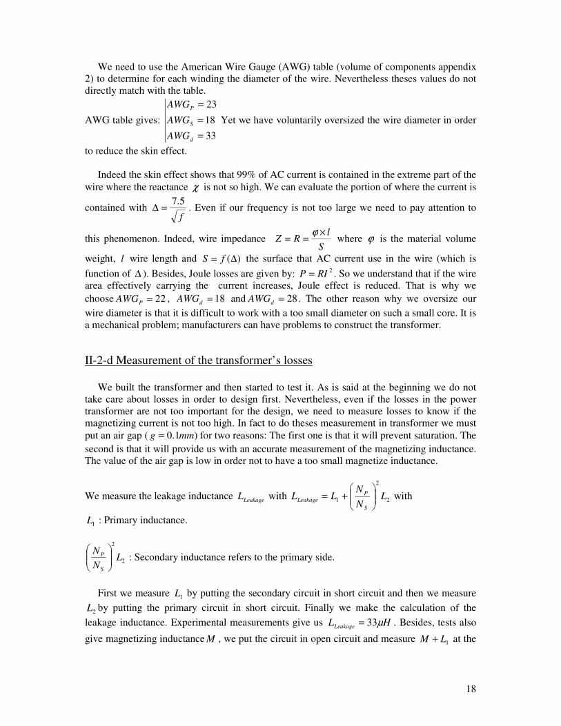
We need to use the American Wire Gauge (AWG) table (volume of components appendix
2) to determine for each winding the diameter of the wire. Nevertheless theses values do not
directly match with the table.
AWG table gives:
33
18
23
=
=
=
d
S
P
AWG
AWG
AWG
Yet we have voluntarily oversized the wire diameter in order
to reduce the skin effect.
Indeed the skin effect shows that 99% of AC current is contained in the extreme part of the
wire where the reactance χ is not so high. We can evaluate the portion of where the current is
contained with f
5.7=∆ . Even if our frequency is not too large we need to pay attention to
this phenomenon. Indeed, wire impedance S
lRZ
×==
ϕ where ϕ is the material volume
weight, l wire length and )(∆= fS the surface that AC current use in the wire (which is
function of ∆ ). Besides, Joule losses are given by: 2RIP = . So we understand that if the wire
area effectively carrying the current increases, Joule effect is reduced. That is why we
choose 22=PAWG , 18=dAWG and 28=dAWG . The other reason why we oversize our
wire diameter is that it is difficult to work with a too small diameter on such a small core. It is
a mechanical problem; manufacturers can have problems to construct the transformer.
II-2-d Measurement of the transformer’s losses
We built the transformer and then started to test it. As is said at the beginning we do not
take care about losses in order to design first. Nevertheless, even if the losses in the power
transformer are not too important for the design, we need to measure losses to know if the
magnetizing current is not too high. In fact to do theses measurement in transformer we must
put an air gap ( )1.0 mmg = for two reasons: The first one is that it will prevent saturation. The
second is that it will provide us with an accurate measurement of the magnetizing inductance.
The value of the air gap is low in order not to have a too small magnetize inductance.
We measure the leakage inductance LeakageL with 2
2
1 LN
NLL
S
PLeakage
+= with
1L : Primary inductance.
2
2
LN
N
S
P
: Secondary inductance refers to the primary side.
First we measure 1L by putting the secondary circuit in short circuit and then we measure
2L by putting the primary circuit in short circuit. Finally we make the calculation of the
leakage inductance. Experimental measurements give us HLLeakage µ33= . Besides, tests also
give magnetizing inductance M , we put the circuit in open circuit and measure 1LM + at the

19
primary. But because 1LM ≥≥ so we obtain mHM 9.1= . So we are able to calculate the
magnetized current and the power losses in the leakage inductance.
min MdIdtV =
Mf
DV
M
TVI inin
m
max== (10)
AI m 4.1= It is a small value as expected. Indeed, in a forward converter the demagnetizion
current is small.
Thus, now we can measure the power stored in the leakage inductance when the switch is
closed. In order to understand how the calculation is made we can describe the circuit through
an equivalent circuit as is shown in the following diagram.
Figure 14: Equivalent circuit of the Forward converter when the transistor is blocking.
fIN
NILP m
P
S
outLeakageLeakage ×
+
=
2
2
1 (11) (Secondary current is referred to primary side).
WPLeakage 2.5=
This power is an approximation, since we simplified the circuit. Nevertheless, it is not too
high.
II-2-e Thermal dimensioning
A thermal calculation of the transformer is needed. Thus it will tell us if the transformer is
well designed. Indeed, if the maximum temperature that rises into the transformer is less than
the maximum temperature authorized by the component it means that the design is successful.

20
To do the thermal-calculation of the transformer we will use simplified equations that are
usually used by power electronic manufacturers.
Figure 15: Repartition of temperature in the transformer.
First of all we need to calculate the volumetric magnetic power losses into the transformer.
( )24.2
1 fKfKBP ehC +∆= with 10
5
10.4
10.4
−
−
=
=
e
h
K
Kwhich are experimental constants.
Thus 3
1 /124.0 cmWPC =
Yet we need to calculate all the magnetic losses into the central core that is why we
measure his volume. eV
( ) 68.07.5 wee AAV = 37.8 cmVe =
So the magnetic power losses are:
eCC VPP 1= WPC 1.1=
Now we are going to calculate the primary winding losses:
2
1 rmsPPJpWP IRlNP = with cmAl e 4.541 == length of one winding around the central core
and PJR the resistance per meter given by the table at C0100 cmRPJ /000708.0 Ω=
WPWP 17.0=
Besides we do the same for the secondary:
2
2 rmsSSJSWS IRlNP = with 12 ll = and cmRSJ /000280.0 Ω=
WPWS 18.0=

21
Thus the total losses into the transformer are:
CWSWPsesTransfolos PPPP ++=
WP sesTransfolos 42.1=
We need to find the Thermal resistance of our core that we used to build the transformer.
( ) 37.0
23
we
TAA
R =
WCRT /3.18 °=
Finally we know that the Thermal equivalent equation is:
TsesTransfolos RPT =∆ (12)
We consider being in the worst situation it means that the ambient air is CTa °= 50 . Thus
we can find the maximum temperature that can rise in our transformer:
TsesTransfolosaT RPTT +=max
CTT °= 76max
This temperature is very far from the maximum temperature allowed in, both, wires and
magnetic core, which is C°150 . So we can say that our transformer is well designed.
II-3 Output Inductor Design
The output Inductor is a very important component of the forward converter circuit. Indeed
it filters the AC component and delivers the DC component of the current that will supply the
load.
II-3-a Determination of the inductance’s value
Thanks to the Kirshoff law, when the switch is conducting we have:
1
2 TLf
VUI out
L
−=∆
max
max
DLf
VVDN
NV
N
N
I
Fin
P
S
in
P
S
L
−
−
=∆

22
( )
fI
DVDVN
N
LL
Fin
P
S
∆
−−
=
maxmax1
(13) with LI∆ the current peak to peak, outL II 4.0=∆
is a simplified relation used by manufacturers. AI L 2=∆
HL µ155=
II-3-b Determination of the inductor core
The inductor core must be determined and then the inductor number of turns. This method
is actually the same as for transformer turn.
The expression of the flux gives us:
NABLI eLPK max==Φ with N inductor number of turns, eLA useful inductor windings
area over the core or inductor central surface of the core and PKI the maximum current that
goes through the inductor AI
II L
outPK 62
=∆
+= .
eL
PK
AB
LIN
max
= (14)
Like for the transformer wLPK kAJNI max= with k inductor winding factor between
primary winding area and window area.
Thus PK
wL
eL
PK
I
kAJ
AB
LI max
max
=
So maxmax
2
JkB
LIAA PK
wLeL = (15)
459.0 cmAA wLeL = This value matches with the E-30/14 type core (volume of components
appendix 1).
Thanks to tables 220.1 cmAeL =
And according (14) 8.25=N 26 turns is adopted for inductor.
Now we need to calculate the RMS current in the winding in order to choose wire
diameter.
II-3-c Determination of the inductor’s wire and air gap
Inductor RMS current:

23
AII rmsLPK 6==
Thus, thanks to the wire table (volume of components appendix II) 16=LAWG . We have
chosen less than what the table gives us because in fact PKrmsL II ≤
Finally the Air Gap ( lg ) into the inductor is the last thing to design. Indeed Air Gap is the
place where most parts of inductor energy is stored. Air gap is linked to inductance and
reluctance by the equation that follow.
L
AN eL0
2
lgµ
= (16) with usi7
0 10.4 −= πµ and eLA
l0
lgRe
µ= the reluctance.
mm65.0lg =
Besides, we designed the output inductor and tested it in order to know if the design
matches with what we built. First we need to measure the inductance. With the Air Gap value
of mm6478.0lg = we obtained HL µ127= .
Thus we notice that if we reduce the Air gap we will increase the inductance. After further
manipulations we chose mm4.0lg = and them we obtained HL µ158= which corresponds to
just 102% of the value of the inductance calculated.
II-4 Choice of the INEP components.
We will not build ourselves any components that we would select to conduct our project.
For example diodes, switches, capacitors, resistors and integrated circuit. We will choose
them from commercially available components in order to get the appropriate ones. Yet, in
order to speed up the prototyping process, we have to choose components from the INEP
workshop. Thus, some components will be oversized in order to match with standard
manufacturer values. Besides it will save money to choose standard manufacturer components
(since they are very cheap), rather than ordering accurate ones to manufacturer. Finally it will
also give good result in simulation.
There are three fundamental parameters to choose diodes and switches:
- Switching frequency.
- Rated voltage.
- Average, RMS current and thermal calculation.
For a resistor we need to specify two fundamental parameters:
- Resistance.
- Power losses.
24
The current that flows through these components is responsible for losses and temperature
rise in junction. Thus depending on the current value, thermal dimensioning may be needed.
Finally for capacitor we need the capacitance value and the rated voltage.
Thanks to PSIM software, we can have access to RMS and average currents and voltage
peaks. So, in all this part we will give value that will be obtained through simulation. Besides
we will choose the most accurate components according to this simulation. Then simulate
again to see if it matches with the expected results.
II-4-a Output Capacitor Design
The aim of the output capacitor is to absorb the AC current component in order to prevent
it from flowing through the resistance. Thus the current that flows through the output load is
only a DC current. Nevertheless the output capacitor can’t divert the entire AC current
component from the output inductor. That is why if we look very accurately to output current
it still has some oscillations at the switching frequency.
The design of the output capacitor requires some specific values. Indeed we cannot build
ourselves a capacitor which is too complicated. Thus we need the capacitor voltage CV , the
capacitor peak to peak LI∆ current, but also the minimum capacitance C that is required for
the circuit.
As soon as we know these three values ( CIV LC ,,∆ ) we have to check into tables of a
capacitor manufacturer. One of the most famous capacitors manufacturer is EPCOS. First of
all, as in the output inductor design the current peak to peak adopted was AI L 2=∆ . Thus the
same current peak to peak will be adopted for output capacitor design. According to the CI
waveform:
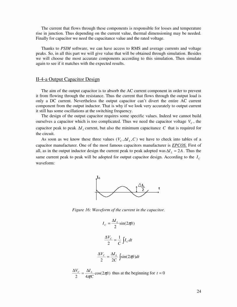
Figure 16: Waveform of the current in the capacitor.
)2sin(2
ftI
I L
C π∆
=
∫=∆
dtIC
VC
C 1
2
dtftC
IV LC
∫∆
=∆
)2sin(22
π
)2cos(42
ftfC
IV LC ππ
∆=
∆ thus at the beginning for 0=t

25
C
L
Vf
IC
∆
∆=
π2 besides usually to design capacitor usually manufacturer take outC VV 01.0=∆
Thus we obtain. VVC 2.0=∆ and FC µ32=
We consider that outC VV ≅ with a tolerance to %40 of load variation of the capacitor
component.
AII
FC
VV
LC
C
2
32
28
min
max
=∆=∆
=
=
µ
Before choosing the capacitor we need to consider the life time of our output capacitor
component. Indeed in our study we decided to design a forward converter circuit for computer
use. Thus the average life time of a laptop computer is around 10 years. To match with tables
and diagram from EPCOS (volume of the component appendix 3 and 4) we will choose a life
time of 11 years.
Besides we must specify in which ambient temperature the output capacitor will work.
Like for the thermal-calculation of the transformer we will consider that the ambient air is at
C°50 (the worst condition that can face the capacitor).
Thus by using diagram we find the ratio RAC
L
I
I
,
∆=2 thus mAI RAC 1000, =
( RACI , is the maximum current that flows through the capacitor for the maximum
temperature authorized in the component C°105 ).
By using the table of capacitor from EPCOS for VVC 35= and for mAI RAC 1000, = we
have to choose the component with mAI RAC 1260, = (nearest value). Thus it gives us the
capacitance of output capacitor:
FC µ2200=
Yet we can’t have such capacitor to conduct our project because it is too expensive. That is
why we will choose in the workshop of the INEP department an output capacitor with
AI
FC
VV
L
C
2
220
35
=∆
=
=
µ
So to respect the information that was given by tables we need to put 10 capacitors that
we chose from the INEP workshop in parallel ( 10220
2200==n ).

26
II-4-b Determination of the switch
We need to know the theoretical value that can be applied on the switch. Maximum
theoretical voltage applied across the switch is according to (2):
+=
d
P
inTN
NVU 1 VUT 667= .
So we consider using the IRFBG20 Mosfet 1000 V/high frequency (available in the
INEP workshop).
Indeed we must choose a MOSFEETMOSFET with maximum voltage higher than the one
given by calculation and simulation.
II-4-c Determination of the heat sink for the switch
The MOSFEETMOSFET will have to be cooled in order not to be destroyed. That is why
we need to calculate the Joule losses in the MOSFEET:
2
rmsTDSMos IRP = (17)
with rmsMosI the efficient current that flows through the MOSFEETMOSFET.
This value can be calculated with complicated mathematical equations. Nevertheless we
prefer to use PSIM software. AI rmsT 92.0= . Besides DSR is the MOSFEETMOSFET on-
resistance, its value depends on MOSFEETMOSFET’s junction temperature. According to
diagram (Volume of components appendix 5) this resistance can be determined for a specific
junction temperature.
We choose to work in the worst situation that the MOSFEETMOSFET can bear. It means
his junction temperature CT j °=100 , this value is usually used by engineers because the
MOSFEETMOSFET is still working normally at this temperature. Above this temperature the
MOSFEETMOSFET performance gets worst and at 150 degrees it gets destroyed. Most of the
time MOSFEETMOSFET junction temperature will be less than this value. Nevertheless, the
chosen component needs to be placed in their temperature mechanical limits in order to have a
good design. So, Ω≈= 2011*8.1DSR . And thus we find:
WPMos 9.16= of losses.
Now we have estimated the losses in the MOSFEETMOSFET. We need to make a
thermal-calculation in order to know if the MOSFEETMOSFET will be able to keep is
junction temperature under CT j °=100 . Indeed, is the MOSFEETMOSFET able to evacuate
power losses (Joule effect) without an external heat sink or not?
Like it was used for the transformer thermal calculation, according (12):

27
thMosMosaj RPTTT =−=∆
withthMosR MOSFEET MOSFET total thermal resistance from MOSFEETjunction to ambient,
with ambient temperature CTa °= 50 .
Figure 17: Equivalent circuit of the MOSFEETMOSFET’s thermal resistance.
First we are going to calculate the junction temperature into the MOSFEETMOSFET
without an external heat sink.
thMosMosaj RPTT +=
with WCRthMos /62°= according to diagram
Thus CT j °≈ 1100
So we can see that this temperature is too high and the MOSFEETMOSFET would be
destroyed. We understand that we must put an external heat sink in order to reduce
MOSFEETMOSFET total thermal resistance. HS 12643 Heat Sink. This kind of external
heat sink is chosen because it is the smallest one in the INEP workshop.
Thus, we choose: ambient air CTa °= 50 and junction temperature CT j °= 100 . We need to
determine the MOSFEETMOSFET total thermal resistance that matches with the junction
temperature needed.
thMosMosaj RPTTT =−=∆ thus
WCP
TR
Mos
thMos /96.2 °=∆
=
So now we have MOSFEETMOSFET total thermal resistance. As it show in thermal
equivalent diagram
thMoshathMoschthMosjcthMos RRRR ++=
We need to evaluate the external heat sink thermal resistance that we will choose.
thMoshathMosjhthMos RRR +=

28
thMosjhthMosthMosha RRR −=
thMosjhR is MOSFEETMOSFET thermal resistance from junction to external heat sink.
So, WCRthMosjh /8.25.03.2 °=+=
WCRthMosha /16.0 °=
Now if we check the diagram, (volume of component appendix 6) that gives us thermal
power evacuated by this external heat sink for T∆ . We can see that this external heat sink is
able to evacuate W5.12 . Yet the power that has to evacuate MOSFEETMOSFET is W.9.16 .
So it is necessary to put a fan while using this external heat sink to provide thermal resistance
that we calculate before. Thus we use diagram that gives us the air speed required by fan to
respect such thermal resistance. In our case we can seen that air speed is 16 −ms .
In fact in an open system configuration it is very difficult to predict the air speed. This air
speed is too important for such a small application. The possibility that can be adopted to
reduce air speed is to use two MOSFEETMOSFETs in parallel. Indeed if the two
MOSFEETMOSFETs are put in parallel the equivalent interne resistance will be divided by
two. 2
DS
DSeq
RR = so the power losses calculated before will be reduce by two.
WPMoseq 45.8=
Besides we can wonder if we still need an external heat sink for these two
MOSFEETMOSFETs. Thus we calculate:
thMosMoseqaj RPTT +=
with WCRthMos /62°= CT j °≈ 574
this temperature is still too high and the MOSFEETMOSFETs will be destroyed. Thus the
external heat sink chose before is still needed.
We use diagram in (volume of component appendix 6) that gives us thermal power
evacuated by this external heat sink for T∆ . We need to evacuate W45.8 (external heat sink
is able to evacuate W5.12 ). So we do not need to put a fan to respect the MOSFEETMOSFET
maximal junction temperature that we have chosen.
To conclude we will adopt MOSFEETMOSFET parallel solution in order to avoid using a
fan in the circuit.
II-4-d Clamping Circuit Design

29
The equivalent circuit that we introduced before (diagram 14) can’t work in reality. Indeed
the Leakage inductance stores energy that it will give to the switch in a very short period of
time when it is opened. This energy delivering into the switch will create a huge voltage
across it and will be able to destroy the switch. The temperature inside the switch will rise to
high value and thermal transfer into the silicon will not be efficient to transfer heat to ambient
air. So the switch will blow. That is why we need to use a clamping circuit in order to divert
this energy. It we will be designed for the maximum duty cycle.
Figure 18: Equivalent circuit of the Forward converter when the transistor is blocking with
the clamping circuit.
The figure that follows shows the importance of the clamping circuit in order to limit the
voltage across the switch due to leakage inductance. We need to design the clamping circuit
and especially the clamping resistance that will limit the voltage across the switch.
Figure 19: wave form of the IGBT.
In fact the power delivered to the clamping circuit is more than the power stored into the
leakage inductance. Leakageclamp KPP = with K a constant given by the expression :

30
clamp
in
U
VK
21
1
−
=
We must choose the voltage clamping that we would like to expect in the clamping circuit.
The theoretical maximum voltage applied across the switch is VUT 667= . We consider that
difference between maxTU and clampU when the impulsion is done will be V115 (value that
can support the switch chosen). Thus VU clamp 781= . So 3.4=K and WPclamp 22≈
Besides (16) give us clamp
clamp
clampR
UP
2
= thus we find the theoretical value the clamping
resistor:
Ω= kRclamp 7.27
Then we simulate the circuit with PSIM and we obtain the result that follow:
For Ω= kRclamp 28 VU clamp 714= and VUT 664max =
Thus the difference between these two voltages is less than V115 so we will adopt:
Ω= kRclamp 28
Then we must select diode and capacitor. According to simulation diode rated voltage and
average current are:
VU Dclamp 707= and AI Dclamp 027.0=
Then we choose Diode type MUR1100/1000V/1A/high frequency. Because DclampI is very
small in comparison with A1 . We understand that the power losses will be very small in it, so
any external heat sink is required. For the capacitor we can calculate theoretically the value of
the capacitance.
VfU
PC
clamp
clamp
clamp∆
= with VV 10=∆ (voltage peak to peak), value usually taken by
manufacturers. Thus we obtain nFCclamp 56=
So, we choose nFCclamp 60= which is an industrial value.
II-4-e Choice of the diodes
Aims of 1D and 2D Diodes are to prevent negative current to flow through transformer
secondary and to allow freewheeling during demagnetizion time. Dm aim is to allow
demagnetization into the transformer.
Theoretical voltage into the secondary is VVN
NU in
P
S 672 ≈= and 22 UU D ≤ . Besides, the
maximum voltage that can drop theoretically into Dm diode is VVU inDm 6002 == thus we

31
have to choose a diode with maximum rated voltage is equal to VVin 7505.2 = for safety
reason.
Rated voltage and average current of these diodes given by simulation are:
For 1D VU D 811 = and AI D 7.11 =
For 2D VU D 652 = and AI D 35.32 =
For Dm VU Dm 540= and AI Dm 13.0=
Thus we choose for 1D and 2D DIODE MUR810/100V/8A/high frequency and for
Dm DIODE MUR1100/1000V/1A/high frequency.
II-4-f Diode thermal calculation
It is no use making a thermal calculation for Dm diode because AI Dm 13.0= is very
small compare to A1 .
But we must calculate power losses across 1D and 2D :
Figure 20: Equivalent representation of a diode.
11 DFD IVP = with FV the voltage drops into the diode. VVF 1= (volume of components
appendix 6) and 22 DFD IVP = .
WP
WP
D
D
35.3
7.1
2
1
=
=
In fact tables do not give us diode total thermal resistance junction-ambient air.
Nevertheless the diode used has a similar structure as the MOSFEETMOSFET. That is why
we will choose as an approximation the following:
WCRRR thMosthDthD /6221 °===
and WCRRR thMosjhjhthDjhthD /8.25.03.221 °=+===
First we are going to calculate the junction temperature in 1D and 2D diodes without an
external heat sink.

32
thDDaj RPTT 11 +=
Thus CTCT jj °≈°≈ 258155 21
So we can see that temperatures which can rise into diodes without external heat sink
being too huge for 1D and 2D diodes. They will be destroyed. Like for the MOSFEET we
need to put external heat sink in order to put diodes into the worst situation that can occur
without destroying it. For the same reason we choose HS 3512 Heat Sink.
Ambient air CTa °= 50 and maximum junction temperature CT jD °= 100
So, CTTT ajD °=−=∆ 50
Total thermal diode resistance is given by:
WCP
TR
WCP
TR
D
D
thD
D
D
thD
/9.14
/4.29
2
2
1
1
°=∆
=
°=∆
=
We need to evaluate external heat sink thermal resistance in order to respect maximum
junction temperature.
jhthDthDhathD RRR 111 −=
Thus we obtainWCR
WCR
hathD
hathD
/1.12
/6.26
2
1
°=
°=
Now if we check the diagram, (volume of components appendix 7) that gives us thermal
power evacuated by this external heat sink for DT∆ . We can see that this external heat sink is
able to evacuate W5 . Thus we understand that the heat sink is oversized for these diodes
because the maximum power that diodes have to evacuate is W35.3 . Nevertheless we keep
this external heat sink because it is the smallest one that we can find in the INEP workshop.
Yet if we had wanted to save money we would have reduced the size of the external heat
sink just to match with an evacuate power of W5.3 .
External heat sink use fins in order to increase their surface to deliver to ambient air more
heat. So reducing the surface will reduce the power evacuated by the heat sink.

33
III Auxiliary Power Supply (Gate driver circuit)
The auxiliary power supply creates the gate signal for the transistor of the forward
converter in order to control the commutations.
Figure 21: The auxiliary circuitry.
III-1 Driver and integrated circuit
Driver and integrated circuit are components needed to create the gate signal that
commands switching of the power stage. Nevertheless driver and integrated circuit also need
a control system provide a well regulated output voltage. Yet, in a first phase, we will design
the gate driver integrated circuit without feedback control. Indeed we will test these two
components over the power stage and manage the duty cycle thanks to a variable resistor. In
order to realize an auxiliary power supply we will follow these steps:

34
Gate driver design.
Choice of the integrated circuit.
Auxiliary power supply test.
III-2 Gate driver design.
To keep the isolation between the input and the output of the power stage, we need to
design a driver in order to assure this function (figure 21). Thus we understand that if we want
to provide isolation to integrated circuit we need to design an isolated gate driver.
As we can see the driver circuit looks like a small forward converter, supplied by a small
power application of V15 . This value comes from maximum gate to source voltage of switch
power VVGS 20= (volume of components appendix 5). This small power will also supply the
integrated circuit and then needs to be isolated. We could have designed this small power
supply but it would have taken too much time. We will use a small, commercially available
power supply.
Figure 22: External power supply scheme.
It uses a small isolated transformer at low frequency ( kHz6 ) that provides small power
( W2≈ ). Now we must design our driver. It looks like a small forward transformer which
doesn’t use an output inductor and an output capacitor. We will use the same equation as used
in part II to design all the component of the driver stage. First we need to give project data
that will be used to design this small circuit:
TB
TB
cmAJ
k
k
k
D
kHzf
AI
WP
VV
AI
WP
VVV
p
w
outd
outd
outd
ind
in
dinind
3.0
3.0
/450
7.0
5.0
4.0
45.0
50
8.0
33.0
5
15
42.0
25.6
15
max
2
max
max
min
=
=∆
=
=
=
=
=
=
=
=
=
=
=
=
== η
These data are close to the reality. Most of them come from the second part data and from
software simulation. Before starting the transformer calculation we need to precise the data
value chosen and notably why the output power of the driver is WP outd 5= . The power needed
for the gate of power stage switch is the same as the power needed to load the capacitor inside

35
the MOSFEET gate. We have access to the capacitance according to switch table (volume of
components appendix 5). pFCiss 500=
Thus WfVCP GSissoutd
3210.8.2
2
1 −== . It is too small a power value. We choose WP outd 5= .
Choosing this power means that we are going to oversize again the driver transformer.
Oversizing the transformer is needed for two specific reasons. First if we design too
accurately our transformer we will face mechanical problem to build it. Second INEP
workshop doesn’t have too small core transformer. Besides we keep the other values from the
power stage design because our transformer won’t be accurate, it doesn’t matter if we keep
the same values.
III-2-a Design of driver transformer core
As was done in the second part we use the same equation (6). 4056.0)( cmAA dwe =
We chose 408.0)( cmAA dwe = this value matches with the E-20 type core (volume of
components appendix 1). So, 2312.0 cmAed =
III-2-b Number of wire turns
According to (7) 4.14=PN 15 turns is first adopted. To simplify the design we choose
to have the same input and output voltage in the driver. So, 15=== dsP NNN . Even if the
number of turns is the same the demagnetization will be fulfilled.
III-2-c Wires diameter
We have the same RMS current (efficient current) in each winding. AI
I outd
rms 23.02
== .
So, 29=driverAWG . We also reduce the skin effect because we have oversized our design.
III-2-d Measure of the driver transformer’s losses
We put an air gap mmg 3.0= in the transformer that we built. And we measure
inductances HLdLeakage µ8.12= , HM d µ8.19= and (10) give us AI md 7= . So the
magnetized current is too important for such a small application. It will destroy our driver
circuit. The only way to reduce such current while keeping the same air gap is to increase the
number of turns. We proceed with the same equation (16) as for the input inductor.
l
NM d
Re
2
= with lRe the reluctance of the core. Thus 610.5.11Re =l is calculated for 15
turns. So we can evaluate the magnetizing inductance needed to design transformer with
having a magnetized current of A1 .
FfI
DVM
md
ind
d µ137max =≥

36
Finally 40Re == lMN d . So we build a new driver transformer with the same
characteristics but we adopt 40 Turns and an air gap. Finally, we test it and we obtain.
HLdLeakage µ2.32= , HM d µ138= and AI md 97.0= and we get WPdLeakage 4.1= these losses
stored in the leakage inductance are not too high for this small application.
III-2-e Heat calculation
Driver transformer is over designed for an output power 2000 times higher than it is
needed. That is why it is not required to make a thermal calculation. We truly know that the
temperature into the transformer will never rise to the maximum temperature allowed by the
component even if it the worst situation (maximum ambient air temperature).
III-3 Determination of the driver switch
As was done in part II we will choose components from the INEP workshop. That is why
some component will be over size to match with manufacturer values. Driver is a very small
power application thus it will be useless to make thermal calculation for components.
The driver switch is connected to the integrated circuit. Its commutation state changes,
because of the integrated circuit. Thus it will provide the commutation operation of the power
stage switch. Theoretical maximum voltage applied across the switch is: indTd VU 2=
VUT 30= . Efficient current that flows through driver switch is AI rmsTd 29.0=
RMS current is so small that thermal calculation is useless and we don’t need to put an
external heat sink. So we consider using an IRF532/MOSFET/ 100V/high frequency
(available in the INEP workshop).
III-4 Driver circuit protection Design
Like in part II we have to design a protection circuit, (figure 21) notably for driver switch
(cdD ,
ZdD ) but also for the gate power stage switch (ZGD ,
GR ) and gate driver switch
(ZtdD ,
dR ).
We will use software simulation to get the required electrical values, and then we will choose
the closest components needed available in the INEP workshop.
III-4-a Switch gate power stage protection
The power stage switch gate must be protected since characteristics of the power stage
switch prevent us from applying on it more than V20 (volume of components appendix 5).
Thus we must select a ZenerZener diode to prevent high voltage rising and a resistor. So we
want to have a maximum voltage of V20 applied to the gate. Besides according to simulation
VU ZG 8.14= and AI RG 2.0= thus we choose Zener Diode/20V/1A/high frequency ( ZGD ).

37
The resistor resistance is given by the equation: Gissr RCt 2.2= with nst r 17= : rise time
given by MOSFET characteristic, pFCiss 500= the capacitance of interne gate capacitor
(inside the power stage switch).
So, Ω= 4.15GR . Yet this value is not a commercial value. Thus we choose Ω= 22GR .
Besides, there is another parameter to select the appropriate resistor. We must know the losses
expected into this resistor. According to the introduction of part III, fixed output power to
design driver circuit is W5 . We expect that power losses in the resistance must be 20 times
less than this. Power losses in the resistor must be W110.5.2 −
.
III-4-b Driver switch protection
We will use a standard diode ( cdD ) and a ZenerZener diode ( ZdD ) in this circuit. The aim
of Zener diode is to protect driver switch from high voltage rising. Diode rated voltage and
average current are: VU cd 3.13= and AI cd 002.0= . Thus we choose MUR810/100V/1A/high
frequency for the standard diode. We want to have a maximum voltage of V40 applied to the driver switch. Besides thanks
to simulation rated Zener voltage is VU Zd 40= and AI cd 002.0= . So, we choose Zender
Diode/40V/1A/high frequency for the Zener diode.
III-4-c Driver switch gate protection
As in power stage the gate of this small switch must be protected. We proceed in the same
way and taking the same component ( Gd RR = and ZGZtd DD = ). Even if it is oversize we are
sure that the gate will be protected, besides they are the smallest components available in
INEP.
III-4-d Driver demagnetizion diode.
As in power stage this diode allows demagnetization of the driver transformer. The
maximum voltage that can drop theoretically into Dmd diode is VVU indDmd 302 == thus
we have to choose a diode with maximum rated voltage is equal to :
VVin 755.2 =
Rated voltage and average current of these diodes given by simulation are VU Dmd 30= and
AI Dm 004.0= so we choose MUR810/100V/1A/high frequency.

38
III-5 Integrated circuit.
The PWM control integrated circuit provides the duty cycle and the elements to implement
the control for a basic dc-dc converter. In fact the duty cycle is generated by the comparison
between a triangular signal and a continued signal. Thus Integrated circuit is a very
complicated component since it uses miniaturized transistors and comparators. We will
choose one from the INEP workshop. The main one available and suitable for this kind of
application is: INTEGRATED CIRCUIT UC3525.
First we are going to design the external components needed to connect the integrated
circuit to the power circuit. These external components enable us to settle the integrated
circuit operating conditions. To fulfill this design we will use integrated circuit characteristics.
In the first design a variable resistor ( PR ) will be used to control manually the duty cycle and
see if results expected by simulation are accurate as it can be seen in the figure 23.
Figure 23: The PWM integrated circuit.
FC µ58 = , FC µ115= and Ω= kRT 86.2 are given by the integrated circuit tables (volume of
components appendix 8). The component TC Ct and TR fixed the frequency for the integrated
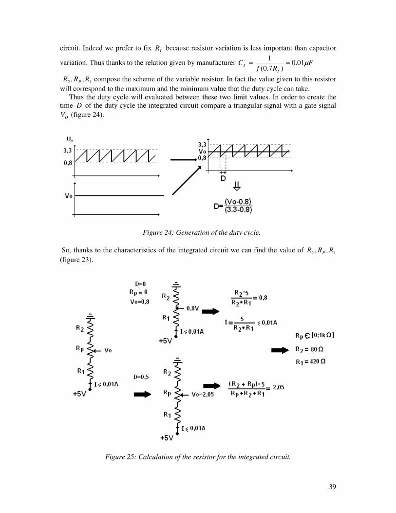
39
circuit. Indeed we prefer to fix TR because resistor variation is less important than capacitor
variation. Thus thanks to the relation given by manufacturer FRf
CT
T µ01.0)7.0(
1==
12 ,, RRR P compose the scheme of the variable resistor. In fact the value given to this resistor
will correspond to the maximum and the minimum value that the duty cycle can take.
Thus the duty cycle will evaluated between these two limit values. In order to create the
time D of the duty cycle the integrated circuit compare a triangular signal with a gate signal
OV (figure 24).
Figure 24: Generation of the duty cycle.
So, thanks to the characteristics of the integrated circuit we can find the value of 12 ,, RRR P
(figure 23).
Figure 25: Calculation of the resistor for the integrated circuit.

40
For more safety we will take the double for all the resistors. To conclude the different
connections are given in the volume of components appendix 8. Then we could give the last
scheme (figure 26) to the technicians and then confirm our result with our prototype.
Figure 26: General scheme for the technicians.

41
IV Test of the laboratory prototype
We start to test the built prototype. We proceed step by step in order to prevent the
destruction of components if we need to adjust some value. Thus we connected each part of
the full circuit one by one.
IV-1 PWM integrated circuit test
First we test the IC that will provide the duty cycle. After observing waveform of the IC
we noticed that we were at saturation in the driver. The duty cycle was higher than 0.5
because the first value chosen for the variable resistor was too high. We decided to limit the
duty cycle from 0 to 0.5 through an easy operation. Indeed there are two outputs of the IC
that provide duty cycle. Both are displaced of 180° . Thus, if we connect both of them
together the duty cycle will be generated between 0 and 1. Besides each output has the same
frequency. Thus if we sum both by connecting them together the frequency will be the half.
So we decided to short circuit the 14 output and thus to multiply frequency by two in order to
keep the same frequency. So we find the new capacitor FRf
CT
T µ05.0)7.0(2
1== that we
must include in our IC (we kept the same resistor TR ).
After testing it again we notice that the transformer driver was never saturated for different
values of the variable resistor because the duty cycle was now limited between 0 and 0.5.
IV-2 Driver circuit test
In the driver we faced only one problem with the resistor GR . Indeed we under evaluated
the power losses in this resistor. The losses are given by (16) G
G
GR
VP
2
= . In fact maximum
value that can reach GV is less than V15 since the driver transformer has a turn ratio of 1. So
the losses that can support this resistor is WPG 5≈ which is too high since the driver circuit
was designed to provide W5 . The resistor used can only withstand W1 . So it would be destroyed. The losses come from the discharge of the inner capacitor of both power stage
switches and provide a negative current through the resistor. One option to reduce these losses
and so to minimize this negative current is to integrate into the PC board the scheme that
follows.
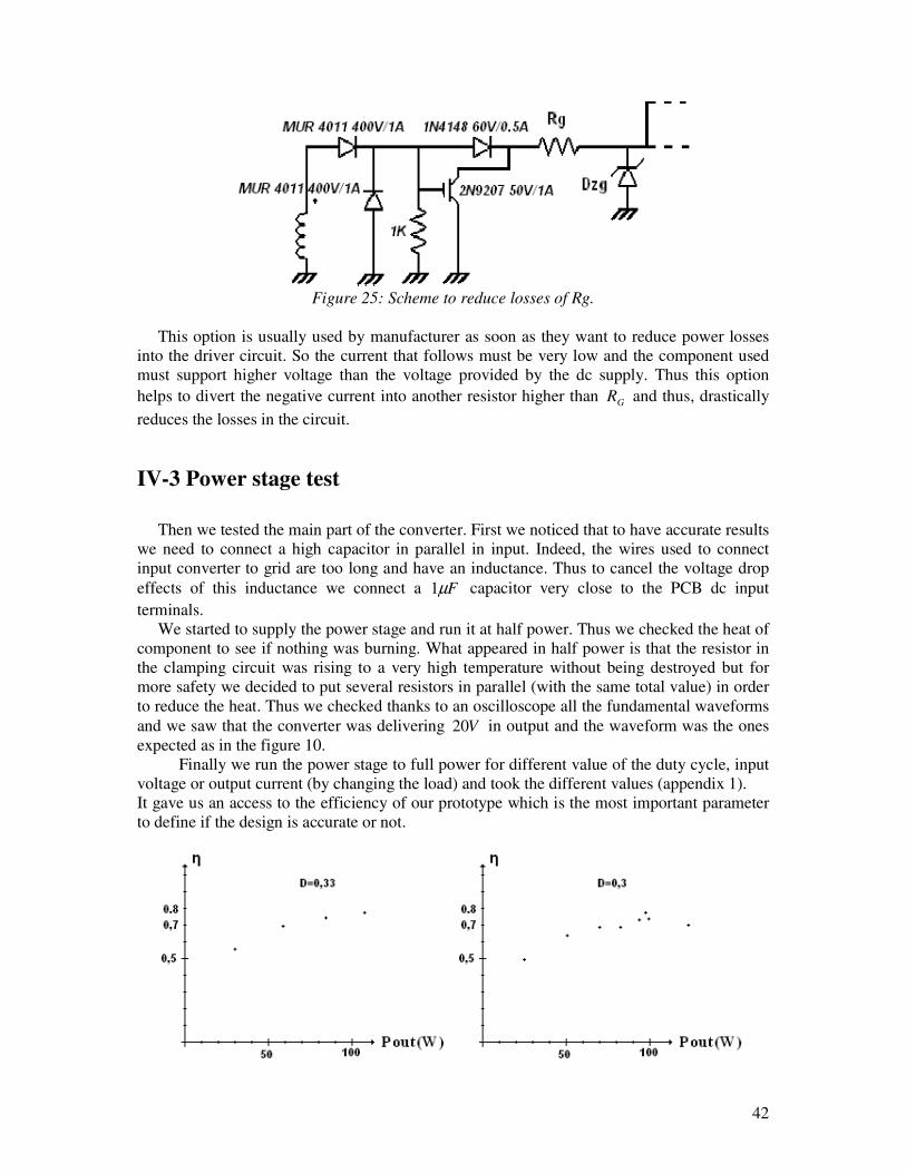
42
Figure 25: Scheme to reduce losses of Rg.
This option is usually used by manufacturer as soon as they want to reduce power losses
into the driver circuit. So the current that follows must be very low and the component used
must support higher voltage than the voltage provided by the dc supply. Thus this option
helps to divert the negative current into another resistor higher than GR and thus, drastically
reduces the losses in the circuit.
IV-3 Power stage test
Then we tested the main part of the converter. First we noticed that to have accurate results
we need to connect a high capacitor in parallel in input. Indeed, the wires used to connect
input converter to grid are too long and have an inductance. Thus to cancel the voltage drop
effects of this inductance we connect a Fµ1 capacitor very close to the PCB dc input
terminals.
We started to supply the power stage and run it at half power. Thus we checked the heat of
component to see if nothing was burning. What appeared in half power is that the resistor in
the clamping circuit was rising to a very high temperature without being destroyed but for
more safety we decided to put several resistors in parallel (with the same total value) in order
to reduce the heat. Thus we checked thanks to an oscilloscope all the fundamental waveforms
and we saw that the converter was delivering V20 in output and the waveform was the ones
expected as in the figure 10.
Finally we run the power stage to full power for different value of the duty cycle, input
voltage or output current (by changing the load) and took the different values (appendix 1).
It gave us an access to the efficiency of our prototype which is the most important parameter
to define if the design is accurate or not.

43
Figure26: Efficiency functions of output power.
We can see that to have the exact value of V20 in output for V300 in input the duty cycle
must be 31.0=D unless the efficiency is %74=η . We obtained the best efficiency around
%77 around the input values which were used for the design of our forward. The efficiency
reach its limit around Pout=100W which was expected.
So, we succeed in the realization of our forward converter because the experimental tests
showed that waveforms and values were close to the ones which were expected.
V Control design and final test
Forward converter provide dc supply to very sensitive electronic loads. Thus if the
voltage deliver to this electronic load (in our case a laptop computer) changes too much they
can be destroyed.
Figure29: Efficiency functions of output power.
That is why a control circuit is needed to adjust the duty cycle as soon as a parameter
changes in order to keep always the same value of the output voltage.
Voltage can change if input voltage changes, if the load changes, if the temperature
changes. To conclude the output load is intolerant to output voltage variation. That is why an
accurate control is needed.

44
Figure30: Appropriate representation for the transfer function
We simplify the circuit by an equivalent circuit which is the appropriate representation in
order to deduce main transfer function of the control circuit (figure 30).
In this process we need to deduce the transfer function of the power stage. After analysis
his bode representation, we can deduce the type of controllercontroller that we need. Indeed
the controllercontroller will help to have a full system stable and as fast as possible.
V-1 Pulse with modulator (PWM)
The PWM is a component inside of the integrated circuit (input points1 and 2 , both
connected to output9 .). It aims is to compare an ideal voltage with voltage that is required at the power stage output. A reference voltage is provided by the IC. According to the table
(volume of components appendix 8) the reference voltage is V1.5 . Resistors 1R and 2R are
needed to connect the output load to the PWM. We must determine resistors, the calculation is
made for VVout 20= 25.020
1.5
21
1 =+
==RR
R
V
V
out
mes , besides we also want to limit the power
losses of theses resistors
8
1)(
2
2
1
2
≤−
+R
VV
R
V mesoutmes
So we deduce Ω= 8161R and Ω= 23842R . Later commercial values will be used and we
will connect these resistors to the PC board.
V-2 Power stage transfer function
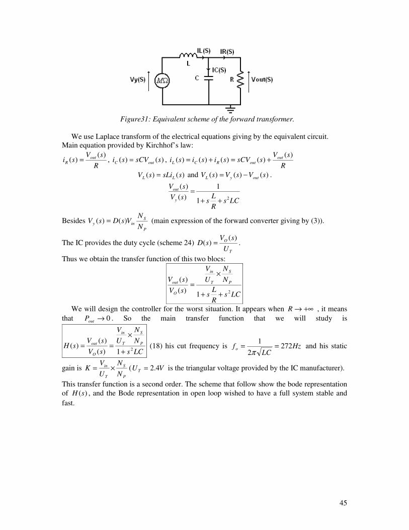
45
Figure31: Equivalent scheme of the forward transformer.
We use Laplace transform of the electrical equations giving by the equivalent circuit.
Main equation provided by Kirchhof’s law:
R
sVsi out
R
)()( = , )()( ssCVsi outC = ,
R
sVssCVsisisi out
outRCL
)()()()()( +=+=
)()( ssLisV LL = and )()()( sVsVsV outyL −= .
LCsR
Ls
sV
sV
y
out
21
1
)(
)(
++
=
Besides P
S
inyN
NVsDsV )()( = (main expression of the forward converter giving by (3)).
The IC provides the duty cycle (scheme 24) T
O
U
sVsD
)()( = .
Thus we obtain the transfer function of this two blocs:
LCsR
Ls
N
N
U
V
sV
sVP
S
T
in
O
out
21)(
)(
++
×
=
We will design the controller for the worst situation. It appears when +∞→R , it means
that 0→outP . So the main transfer function that we will study is
LCs
N
N
U
V
sV
sVsH P
S
T
in
O
out
21)(
)()(
+
×
== (18) his cut frequency is HzLC
fo 2722
1==
π and his static
gain is P
S
T
in
N
N
U
VK ×= ( VUT 4.2= is the triangular voltage provided by the IC manufacturer).
This transfer function is a second order. The scheme that follow show the bode representation
of )(sH , and the Bode representation in open loop wished to have a full system stable and
fast.

46
Figure32: (A) Bode diagram of the power stage (B) Ideal Bode diagram for a fast and stable
system.
The cut frequency wishes is fix by us, but it has to respect the Shannon’s theorem.
)(210
Shannonff
f c ≤≈ so kHzf c 5= .
So to obtain this ideal Bode diagram we must add a controller before the PWM.
V-3 Controller transfer function
The controllercontroller aims is to provide stability and rapidity to the full system. That is
the most important element of the control circuit. Thus we must design this component to get
an a bode diagram close from the ideal one. In a forward converter, the controller usually used
by manufacturers is the one that follow (figure 31).
Figure33: Scheme of the controller.
Manufacturers choose this type of controller because its Bode diagram is appropriate to
obtain a full system stable and fast.

47
Figure34: (A)Bode diagram of power stage and controller (B)Sum of the two Bode diagram
from (A)
The controller transfer function is
)1)((
)1)(1()(
ipiz
izip
iizipf
fzfiiz
RR
RRsCRRsC
sRCsCRsG
+++
++= (19)
This expression comes from the circuit analysis that we won’t detail. We have to determine
the different components of this controller ffzizi CRRC ,,, .
We must use equations given by transfer function and Bode diagram analysis.
Thus we obtain four equations:
01 =Pf , izi
ZRC
ffπ2
101 == ,
fzf
ZRC
ffπ2
102 == ,
)(2
1102
ipiz
izip
i
CP
RR
RRC
ff
+
==
π
))((
1))((
cdB
cdBfHG
fGG = .
By using MAPPLE software we solve this system of equations. So we obtain nFCi 3.5= ,
Ω= kRiz 111 , Ω= kR fz 91 , nFC f 4.6= , Ω= 607iPR , Ω= kRref 6,111 .
Beside we need to take commercial values so we will adopt: Ω= 8201R , Ω= 22002R ,
nFCi 6.5= , Ω= kRiz 120 , Ω= kR fz 82 , nFC f 8.6= and Ω= kRref 120 . iPR is replace by 1R
and 2R in parallel.
V-4 Final test.
Before building the control circuit we test elements by numerical simulation to check if the
control is operating well. Thus we can see that the designed circuit is working. Indeed if
output load change quickly the control changes rapidly the duty cycle in order to still deliver
V20 in output. Besides the time correction is small. So we built the controller and test it on the PC board. We can see that the control is operating, the output voltage was regulated and
fixed at V20 even if the load changes. Nevertheless we were not able to supply the circuit
with more than VVin 180= . Indeed noise appears into the output inductance. The noise was

48
produce by too high frequency, which makes the inductance core tremble. Thus one solution
to reduce noise is to filter high frequency emissions by adding another capacitor in parallel of
fzR and fC .
By adding this new capacitor we create a new pole in system transfer function that cut high
frequency at kHzf c 2= . (Simulation allow us to measure the value of the frequency cut) First
we used nFC 100=+ . We notice that noise disappeared and regulation was sill working.
Nevertheless response to fast load changes was too slow (more than ms10 ). We made a new
numerical simulation to find the appropriate value and to have a rapid answer to load
variations. nFC 1=+ . Finally we test the circuit again. We see that noise disappeared and
control was properly operated.
Besides it was much faster to a load variation than with nFC 100=+ .
To conclude control operates well its main function: to provide quickly the appropriate duty
cycle even if the output load change in order to still have V20 in output. This is the end of the full design of a Forward converter.
CONCLUSION
The design of a Forward converter demands great precision when calculating the different
parameters and restrictions that will have to be applied when conceiving the model. The first
step of the design was the understanding of the Forward converter. The comprehension of the
different waves forms and the link between the transformer, the duty cycle and the input and
output voltage. Once this had been done it was possible to proceed to the forward design and
to see that the transformer was really the heart of the converter. During this phase we went
step by step to design all the circuit elements such as output capacitor and inductor, diodes,
switches, clamping circuit, driver and integrated circuit. We saw that each problem’s solution
made a new one appears which had to be solved to proceed to the other step. The design
appears like a compromise of plenty parameters and can’t be totally accurate. Indeed during
this phase we have to choose commercial values components not too far from the numerical
results. We oversized some components not to face mechanical problems. Finally we made
thermal calculations in order to check if components would not have been destroyed as soon
as they are supplied.

49
The laboratory test shows us how the numerical simulation first used in design was
powerful. Indeed it allows to predict waveforms and to have a first idea of how the
components will react. Besides, during test we faced some problems that showed that at some
points, the circuit was wrong. Numerical simulation completed by laboratory test helped us to
solve these problems. Finally the control of the full system was the last part we studied.
Indeed it appeared that the control was the brain of the converter.
The control provides the security of the converter, it checks if values expected are fulfilled
and adjust parameters if the nature of the circuit changes.
To conclude this project allows us to understand how engineer works to design and realize
a complex power electronics system. Besides we learned how to work with numerical
simulation and calculation softwares, we understanded the method to solve problems in the
design stage but also in the test stage of a project. Thus, one of the best proofs is that we
finally arrived to good results for this system that we entirely calculated and realized. Besides,
this type of power electronics szstem is used today in plenty of consumer electronics such as
laptop computer but also electric engines. It is the first step to introduce to more and more
complicated system.
APPENDIX
Appendix 1: Table of values from experiment of our forward
Input parameters Output values
D Iout(A) Vin(V) Vout(V) Iin(A) Pin(W) Pout(W) η
0,4 7,2 247 19,3 0,75 185 138 74,6%
0,4 3,85 252 20,5 0,43 108 79 73,1%
0,33 1,35 285 21,9 0,19 54 29,5 54,5%
0,33 2,7 285 21,6 0,29 84 58,4 69,5%
0,33 4 285 21,1 0,4 114 84 73,6%
0,33 5,2 285 20,8 0,49 140,5 108 76,8%
0,3 1,2 300 20,8 0,17 52 25 49%

50
0,3 2,5 300 20,2 0,26 78 50,5 64,8%
0,3 3,6 300 19,7 0,35 105 70 67,5%
0,3 4,5 300 18,5 0,41 123 83,2 67%
0,3 4,8 300 19,6 0,43 129 94 73%
0,3 4,9 300 19,9 0,42 126 97 77%
0, 3 5,5 300 18 0,47 134 99 73,8%
0,3 6,5 300 18,4 0,56 168 119 70%
0,31 5 300 20 0,45 135 100 74%
Bibliography
Classical Referencies
[1]Ivo Barbi, 2007. – Electrônica de Potência: Projetos de fonts chaveadas, Florianópolis,
Ediçao do Autor.
[2] Presses Polytechniques et Universitaires Romandes, Philippe Barrade, 2006. –
Electronique de Puissance : Méthodologie et Convertisseurs Elémentaires.
[3] R.R Donnelly and Sons Compagny, Abraham I. Pressman, 1991. – Switching Power
Supply Design.
[4] M. Charpentier lesson, Ecole Navale. – Electronique de Puissance.
[5] Herbert P. Neff, Jr. lesson, University of Tennessee. – Introductory Electromagnetics.
Web Sites
[6] http://www.ivobarbi.com/PDF/LabPotencia08-01/UC3525.pdf
[7] http://www.ivobarbi.com/PDF/LabPot08-02/Circuitos%20de%20Comando_2008.2.pdf
[8] http://www.ivobarbi.com/PDF/LabPotencia08-01/Grampeadores.pdf
[9] http://www.datasheetcatalog.org/datasheet/irf/irfbg20.pdf
[10] http://www.datasheetcatalog.org/datasheet/motorola/IRF532.pdf
[11] http://www.datasheetcatalog.org/datasheet/SGSThomsonMicroelectronics/mXtwqrx.pdf

51
[12] http://www.datasheetcatalog.org/datasheet/SGSThomsonMicroelectronics/mXtxuvq.pdf
[13] http://www.epcos.com/inf/20/30/db/alu_03/03710385.pdf
[14] http://www.hsdissipadores.com.br/catalogo.pdf
[15] http://www.digchip.com/datasheets/parts/mu/parts_mu07.php
[16] http://www.digchip.com/datasheets/parts/datasheet/284/MUR1100.php