Embed Size (px)
Citation preview

Sam PalermoAnalog & Mixed-Signal Center
Texas A&M University
ECEN620: Network TheoryBroadband Circuit Design
Fall 2014
Lecture 3: PLL Analysis

Agenda & Reading
• PLL Overview & Applications• PLL Linear Model• Phase & Frequency Relationships• PLL Transfer Functions• PLL Order & Type
• Reading• Chapter 2, 3, 5, & 12 of Phaselock Techniques,
F. Gardner, John Wiley & Sons, 2005. 2
References
• M. Perrott, High Speed Communication Circuits and Systems Course, MIT Open Courseware
• Chapter 2 of Phase-Locked Loops, 3rd Ed., R. Best, McGraw-Hill, 1997.
• Chapter 2, 3, 5, & 12 of Phaselock Techniques, F. Gardner, John Wiley & Sons, 2005.
3

PLL Block Diagram
[Perrott]
• A phase-locked loop (PLL) is a negative feedback system where an oscillator-generated signal is phase AND frequency locked to a reference signal
4
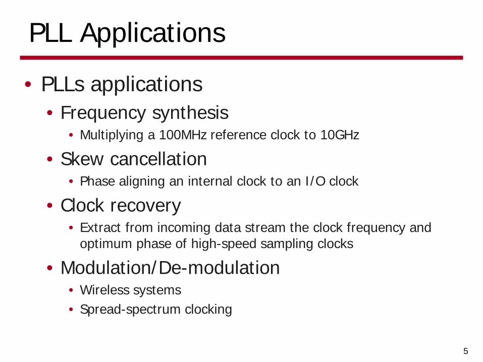
PLL Applications
• PLLs applications• Frequency synthesis
• Multiplying a 100MHz reference clock to 10GHz
• Skew cancellation• Phase aligning an internal clock to an I/O clock
• Clock recovery• Extract from incoming data stream the clock frequency and
optimum phase of high-speed sampling clocks
• Modulation/De-modulation• Wireless systems• Spread-spectrum clocking
5
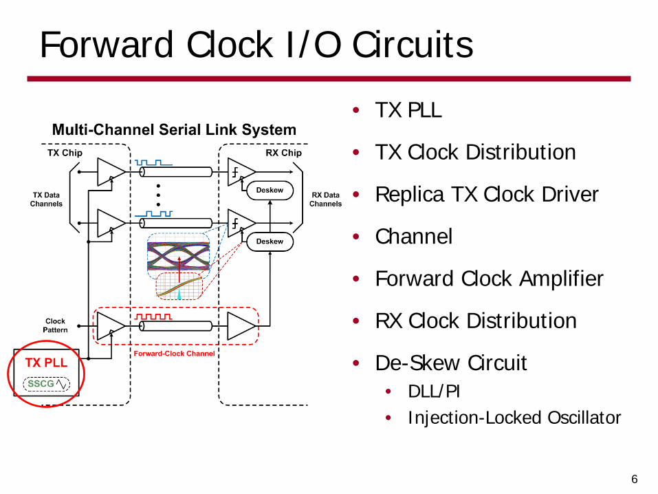
Forward Clock I/O Circuits
• TX PLL
• TX Clock Distribution
• Replica TX Clock Driver
• Channel
• Forward Clock Amplifier
• RX Clock Distribution
• De-Skew Circuit• DLL/PI• Injection-Locked Oscillator
6

Embedded Clock I/O Circuits
• TX PLL
• TX Clock Distribution
• CDR• Per-channel PLL-based• Dual-loop w/ Global PLL &
• Local DLL/PI• Local Phase-Rotator PLLs• Global PLL requires RX
clock distribution to individual channels
7
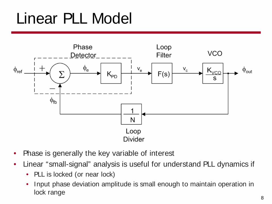
Linear PLL Model
• Phase is generally the key variable of interest• Linear “small-signal” analysis is useful for understand PLL dynamics if
• PLL is locked (or near lock)• Input phase deviation amplitude is small enough to maintain operation in
lock range8
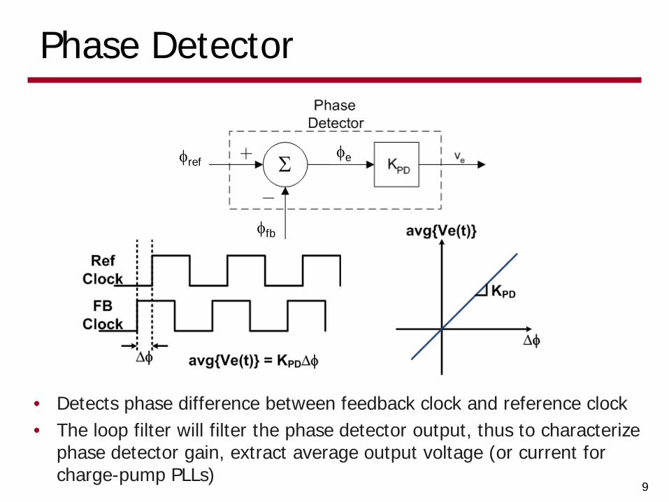
Phase Detector
• Detects phase difference between feedback clock and reference clock• The loop filter will filter the phase detector output, thus to characterize
phase detector gain, extract average output voltage (or current for charge-pump PLLs)
φref
φfb
φe
9
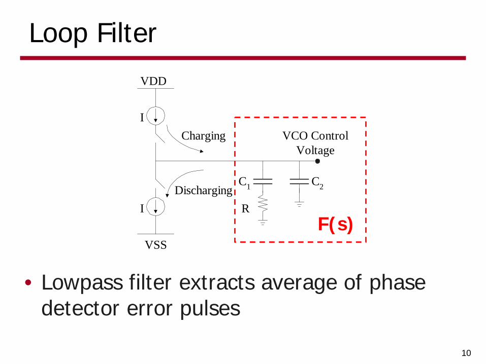
Loop Filter
• Lowpass filter extracts average of phase detector error pulses
I
I
VCO ControlVoltage
C1
R
C2
Charging
Discharging
VDD
VSSF(s)
10

Voltage-Controlled Oscillator
• Time-domain phase relationship
VDDVDD/20
ω0 1KVCO
( ) ( ) ( )tvKtt cVCOoutout +=∆+= 00 ωωωω
( ) ( ) ( )∫ ∫=∆= dtdt tvKtt cVCOoutout ωφLaplace Domain Model
φout(t)
11

Loop Divider
• Time-domain model( ) ( )t
Nt outfb ωω 1=
( ) ( ) ( )∫ == tN
tN
t outoutfb φωφ 1dt1
[Perrott]
φout(t) φfb(t)
12

Phase & Frequency Relationships
• Phase Step
( ) ( )
( ) ( )∫=
=
t
o
t
tdt
ττωφ
ωφ
d
td
phase of time) vschange of (rate derivativefirst theisFrequency Angular
( ) ( ) ( )
( ) ( ) ( )( )ttu
tu
111
111
tsint
phase and tfrequency angular with t sinusoid aConsider
φω
φω
+=
( ) ( )
( ) ( ) ( )( )
frequencyin change No
sin 11
1
tuttu
tut
∆Φ+=
∆Φ=
ω
φ
∆Φ
[Best]
13

Phase & Frequency Relationships
• Frequency Step ( )
( ) ( ) ( )( )
( )
phasein ramp a produces stepfrequency A
where
sinsin
1
1001
01
tt
tttttu
t
ωφ
φωωω
ωωω
∆=
+=∆+=
∆+=
[Best]
( ) tt ωφ ∆=1
14

( )
( ) ( )( )
( )
phasein change quadratic a produces rampfrequency A
2 where
sin2
sinsin
21
102
00
01
01
tt
ttttdtu
tt
t
•
••
•
∆=
+=
∆+=
∆+=
∆+=
∫
ωφ
φωωωττωω
ωωω
Phase & Frequency Relationships
[Best]
• Frequency Ramp
0ω t•
∆+ ωω0
( ) 21 2
tt•
∆=
ωφ
15
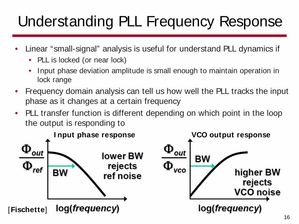
Understanding PLL Frequency Response
• Linear “small-signal” analysis is useful for understand PLL dynamics if• PLL is locked (or near lock)• Input phase deviation amplitude is small enough to maintain operation in
lock range
• Frequency domain analysis can tell us how well the PLL tracks the input phase as it changes at a certain frequency
• PLL transfer function is different depending on which point in the loop the output is responding to
Input phase response VCO output response
[Fischette]16
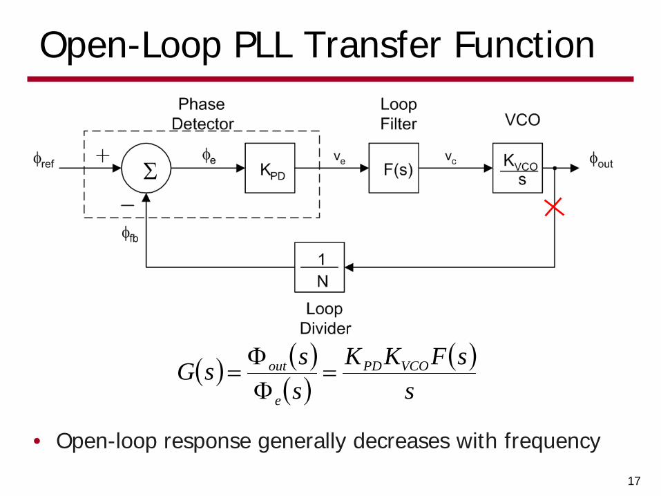
Open-Loop PLL Transfer Function
( ) ( )( )
( )s
sFKKsssG VCOPD
e
out =ΦΦ
=
• Open-loop response generally decreases with frequency
17

Closed-Loop PLL Transfer Function
( ) ( )( )
( )( )
( )( )
NsFKKs
sFKK
NsG
sGsssH
VCOPD
VCOPD
ref
out
+=
+=
ΦΦ
=1
( )
( ) ( )
( ) ( )N
sGN
sG
NsG
sNsFKKl
sG
VCOPD
+=+
−−=∆
=−=∆
−=−=
=
101t Determinan System
101t DeterminanPath Forward
Gain Loop
GainPath Forward
1
1
• Low-pass response whose overall order is set by F(s)
18

PLL Error Transfer Function
( ) ( )( ) ( ) ( )
NsFKKs
s
NsGs
ssEVCOPDref
e
+=
+=
ΦΦ
=1
1
( ) ( )
( ) ( )N
sGN
sG
NsG
sNsFKKl VCOPD
+=+
−−=∆
=−=∆
−=−=
=
101t Determinan System
101t DeterminanPath Forward
Gain Loop
1GainPath Forward
1
1
• Ideally, we want this to be zero• Phase error generally increases with
frequency due to this high-pass response19

PLL Order and Type
• The PLL order refers to the number of poles in the closed-loop transfer function• This is typically one greater than the number of loop
filter poles
• The PLL type refers to the number of integrators within the loop• A PLL is always at lease Type 1 due to the VCO
integrator
• Note, the order can never be less than the type
20

First-Order PLL
• Simple first-order low-pass transfer function
• Closed-loop bandwidth is equal to the DC loop gain magnitude
( )
( )
( )
( )
( )DCdBVCOPD
DCVCOPD
dB
DC
DC
dB
dB
VCOPD
VCOPD
VCOPD
sDC
DCVCOPD
Kss
ss
NKKKs
ssE
KN
KKK
KsNK
sN
NKKKs
KKKsH
NKKK
NssGK
sNK
sKKKsG
KsF
+=
+=
+=
==
+=
+=
+=
=
=
==
=
→
31
13
3
3
1
1
1
0
1
1
:FunctionError
:Bandwidth Loop-Closed
:FunctionTransfer
lim :MagnitudeGain Loop DC
:GainPath Forward
ω
ω
ωω
21

First-Order PLL Tracking Response• The PLL’s tracking behavior, or how the phase error responds to an input
phase change, varies with the PLL type• Phase Step Response
( ) ( )
( ) ( ) ( )( )
frequencyin change No
sin 11
1
tuttu
tut
∆Φ+=
∆Φ=
ω
φ
[Best]
• The final value theorem can be used to find the steady-state phase error
( )( ) 0limlim00
=+∆Φ
=
∆Φ
→→DC
ss KssssE
s
• All PLLs should have no steady-state phase error with a phase step error• Note, this assumes that the frequency of operation is the same as the VCO
center frequency (Vctrl=0). Working at a frequency other than the VCO center frequency is considered having a frequency offset (step).
22

First-Order PLL Tracking Response
• Frequency Offset (Step)
• The final value theorem can be used to find the steady-state phase error
( )( )DCDC
ss KKsssE
sωωω ∆
=+∆
=
∆
→→ 020limlim
• With a frequency offset (step), a first-order PLL will lock with a steady-state phase error that is inversely proportional to the loop gain
( )
( ) ( ) ( )( )
( )
phasein ramp a produces stepfrequency A
where
sinsin
1
1001
01
tt
tttttu
t
ωφ
φωωω
ωωω
∆=
+=∆+=
∆+=
[Best]
23

First-Order PLL Issues
• The DC loop gain directly sets the PLL bandwidth• No degrees of freedom
• In order to have low phase error, a large loop gain is necessary, which implies a wide bandwidth• This may not be desired in applications where we would like to filter
input reference clock phase noise
• First-order PLLs offer no filtering of the phase detector output• Without this filtering, the PD may not be well approximated by a
simple KPD factor• Multiplier PDs have a “second-harmonic” term• Digital PDs output square pulses that need to be filtered
24

Second-Order Type-1 PLL w/ Passive Lag-Lead Filter
( ) ( )
CRCR
sssF
2211
21
2
11
==
+++
=
ττ
τττ
Passive Lag-Lead Loop Filter[Allen]
25
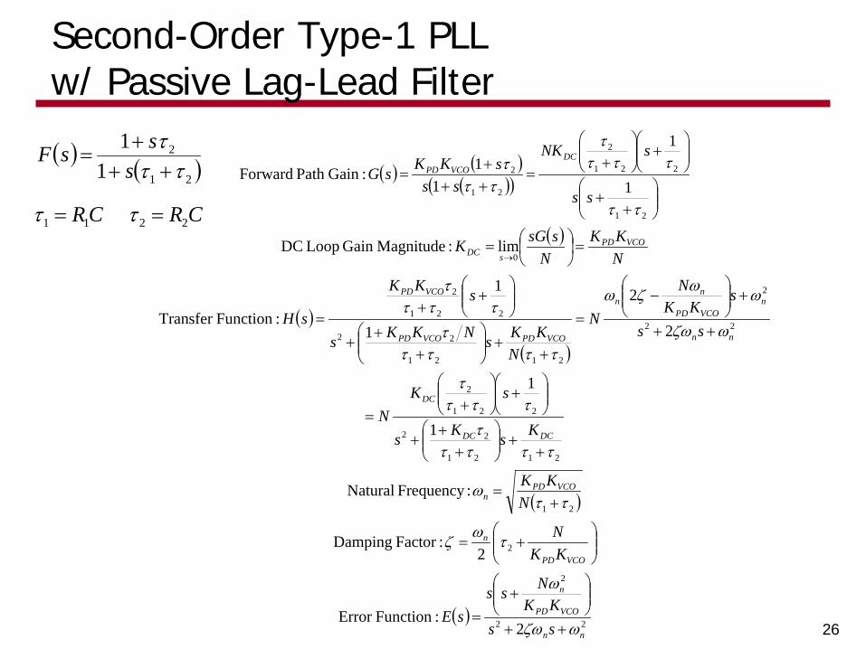
( ) ( )
CRCR
sssF
2211
21
2
11
==
+++
=
ττ
τττ
Second-Order Type-1 PLL w/ Passive Lag-Lead Filter
( ) ( )( )( )
( )
( )
( )
( )
( ) 22
2
2
21
2121
22
221
2
22
2
2121
22
221
2
0
21
221
2
21
2
2 :FunctionError
2 :Factor Damping
:Frequency Natural
1
1
2
2
1
1
:FunctionTransfer
lim :MagnitudeGain Loop DC
1
1
11 :GainPath Forward
nn
VCOPD
n
VCOPD
n
VCOPDn
DCDC
DC
nn
nVCOPD
nn
VCOPDVCOPD
VCOPD
VCOPD
sDC
DCVCOPD
ssKK
NsssE
KKN
NKK
KsKs
sKN
ss
sKK
N
N
NKKsNKKs
sKK
sH
NKK
NssGK
ss
sNK
sssKKsG
ωζω
ω
τωζ
ττω
τττττ
ττττ
ωζω
ωωζω
τττττ
ττττ
ττ
ττττ
τττ
++
+
=
+=
+=
++
+
++
+
+
=
++
+
−
=
++
+
++
+
+=
=
=
+
+
+
+
=+++
=
→
26

• Phase Step Response
( )( )
step phase a with zero be shoulderror phase Again,
02
limlim 22
2
00=
++
+∆Φ
=
∆Φ
→→nn
VCOPD
n
ss ssKK
NssssE
s ωζω
ω
• A second-order type-1 PLL will still lock with a phase error if there is a frequency offset!
Second-Order Type-1 PLL Tracking Response
• Frequency Offset (Step)
( )( )DCnn
VCOPD
n
ss KssKK
NsssE
sω
ωζω
ωωω ∆
=++
+∆
=
∆
→→ 22
2
020 2limlim
27
Second-Order Type-1 PLL Properties
• While the second-order type-1 PLL will still lock with a phase error with a frequency offset, it is much more useful than a first-order PLL
• There are sufficient design parameters (degrees of freedom) to independently set ωn, ζ, and KDC
• The loop filter conditions the phase detector output for proper VCO control
• Loop stability needs to be considered for the second-order system
28

• Note, this type of loop filter is typically used with a charge-pump driving it. Thus, the filter transfer function is equal to the impedance.
Second-Order Type-2 PLL w/ Passive Series-RC Lag-Lead Filter
( )s
RCsR
sF
+
=
1
Passive Series-RC Loop Filter
29

( )
( )
( ) 22
2
222
2
2 :FunctionError
2 :Factor Damping
:Frequency Natural
22
21
:FunctionTransfer
1
:GainPath Forward
(ideally) :MagnitudeGain Loop DC
nn
n
VCOPDn
nn
nn
VCOPDVCOPD
VCOPD
VCOPD
DC
ssssE
RC
NCKK
ss
sN
NCKKs
NRKKs
RCsRKK
sH
sRC
sRKKsG
K
ωζω
ωζ
ω
ωζωζωζω
++=
=
=
++
+=
+
+
+
=
+
=
∞=
Second-Order Type-2 PLL w/ Passive Series-RC Lag-Lead Filter
( )s
RCsR
sF
+
=
1
30

• Phase Step Response
( )( )
step phase a with zero be shoulderror phase Again,
02
limlim 22
2
00=
++∆Φ
=
∆Φ
→→nn
ss sssssE
s ωζω
• A second-order type-2 PLL will lock with no phase error with a frequency offset!
Second-Order Type-2 PLL Tracking Response
• Frequency Offset (Step)
( )( ) 02
limlim 22020=
++∆
=
∆
→→nn
ss sssssE
s ωζωωω
31

Second-Order Type-2 PLL Properties
• A big advantage of the type-2 PLL is that it has zero phase error even with a frequency offset• This is why type-2 PLLs are very popular
• A type-2 PLL requires a zero in the loop filter for stability.• Note, this is not required in a type-1 PLL
• This zero can cause extra peaking in the frequency response• Important to minimize this in some applications, such
as cascaded CDR systems
32

Next Time
• PLL System Analysis• PLL Stability• Noise Transfer Functions• Transient Response
33


![ECEN620: Network Theory Broadband Circuit Design Fall 2019ece.tamu.edu/~spalermo/ecen620/lecture07_ee620_vcos.pdf• VCO Jitter 23. Oscillator Noise 24 Jitter [McNeill] Phase Noise](https://img.dokumen.tips/doc/110x75/5eb0f0afdb23476d411ded00/ecen620-network-theory-broadband-circuit-design-fall-spalermoecen620lecture07ee620vcospdf.jpg)