Embed Size (px)
Citation preview
Sam Palermo Analog & Mixed-Signal Center
Texas A&M University
ECEN620: Network Theory Broadband Circuit Design
Fall 2012
Lecture 16: VCO Phase Noise

Agenda
• Phase Noise Definition and Impact
• Ideal Oscillator Phase Noise
• Leeson Model
• Hajimiri Model
2
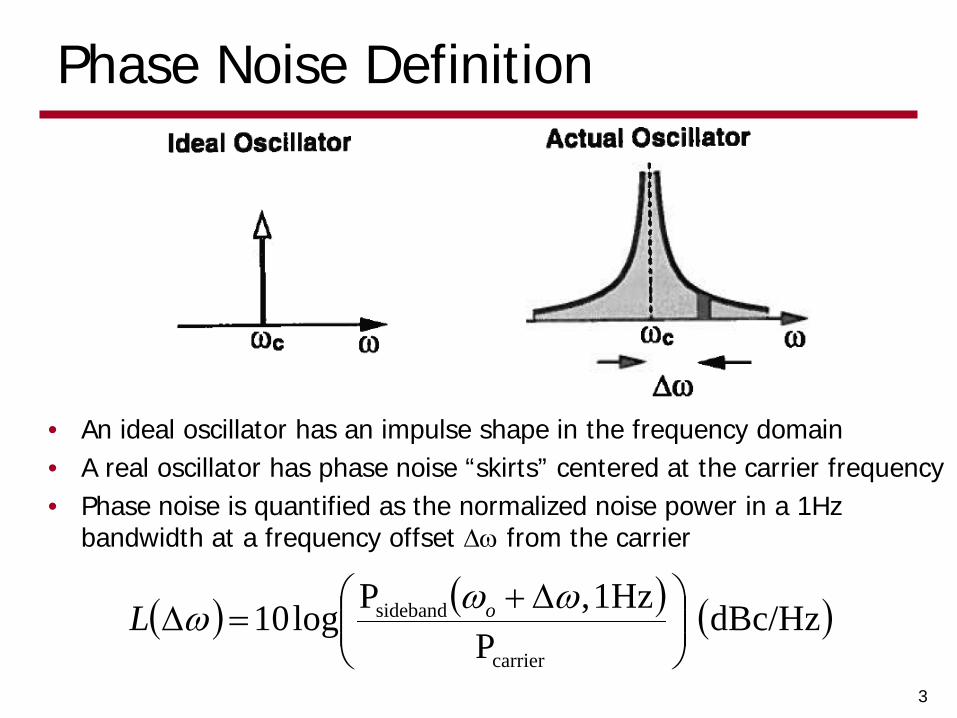
Phase Noise Definition
• An ideal oscillator has an impulse shape in the frequency domain • A real oscillator has phase noise “skirts” centered at the carrier frequency • Phase noise is quantified as the normalized noise power in a 1Hz
bandwidth at a frequency offset ∆ω from the carrier
3
( ) ( ) ( )dBc/Hz P
1Hz ,Plog10carrier
sideband
∆+=∆
ωωω oL

Phase Noise Impact in RF Communication
• At the RX, a large interferer can degrade the SNR of the wanted signal due to “reciprocal mixing” caused by the LO phase noise
• Having large phase noise at the TX can degrade the performance of a nearby RX
4
RX Reciprocal Mixing Strong Noisy TX Interfering with RX

Jitter Impact in HS Links
5
• RX sample clock jitter reduces the timing margin of the system for a given bit-error-rate
• TX jitter also reduces timing margin, and can be amplified by low-pass channels

Ideal Oscillator Phase Noise
6
2tank
22
2
is voltagenoise squared-mean theofdensity spectral The
4
noise thermalintroduce willresistance tank The
Zf
if
v
RkT
fi
nn
n
∆=
∆
=∆
Tank Impedance Near Resonance
7
( )
( ) ( )
( )
( )2
2tank
tank
22tank
2tank
2
2
1 Tank
12221
resonance toclose sfrequencieConsider
1 :Frequency Resonance
11
∆
=∆
∆−≈∆
=⇒=
∆−=
∆−−≈
∆−∆−−∆+
=∆
∆+=
=
−==
ωωω
ωωω
ωω
ωω
ωωωω
ωωωωωωω
ωωω
ω
ωωω
ωω
QRZ
QRjZ
QR
CCRQ
Cj
LCLj
LCLCLCLjZ
LC
LCLjLj
CjZ
o
o
oo
o
oo
o
oo
o
o
o

Ideal Oscillator Phase Noise
8
{ } ( )
carrier thefromaway slope 20dB/dec- adisplay willnoise thermal todue noise Phase
dBc/Hz 2
2log10
phase. and amplitudebetween 21evenly
split ispower noise thisTherefore, equal. arepower noise-phase and amplitude
m,equilibriuin that,states 2000] JSSC [Lee Theoremion Equipartit The
24
24
2
222
tank
22
∆
=∆
∆
=
∆
=
∆=
∆
ωωω
ωω
ωω
QPkTL
QkTR
QR
RkTZ
fi
fv
o
sig
oonn

Other Phase Noise Sources
• Tank thermal noise is only one piece of the phase noise puzzle
• Oscillator transistors introduce their own thermal noise and also flicker (1/f) noise
9
[Perrott]

Leeson Phase Noise Model
10
• Leeson’s model modifies the previously derived expression to account for the high frequency noise floor and 1/f noise upconversion
• A empirical fitting parameter F is introduced to account for increased thermal noise
• Model predicts that the (1/∆ω)3 region boundary is equal to the 1/f corner of device noise and the oscillator noise flattens at half the resonator bandwidth
{ } ( )dBc/Hz 12
12log1031
2
∆
∆+
∆
+=∆ω
ω
ωωω fo
sig QPFkTL

11 ELEN620-IC Design of Broadband Communication circuit
A 3.5GHz LC tank VCO Phase Noise
Measure Phase noise
-30dB/decade -20dB/decade
-105dBc

12 ELEN620-IC Design of Broadband Communication circuit
VCO Output Spectrum Example
-85dBm
-20dBm RBW=10K
PN=-85dBm-(-20dBm)-10log10(10e3)
=-105dBc
dBc---in dB with respect to carrier

Leeson Model Issues
13
• The empirical fitting parameter F is not known in advance and can vary with different process technologies and oscillator topologies
• The actual transition frequencies predicted by the Leeson model does not always match measured data

YCLO
AMSC-TAMU 14
Harjimiri’s Model (T. H. Lee) Injection at Peak (amplitude noise only)
Injection at Zero Crossing (maximum phase noise)

15 ELEN620-IC Design of Broadband Communication circuit
A time-Varying Phase Noise model: Hajimiri-Lee model
Impulse applied to the tank to measure its sensitivity function
The impulse response for the phase variation can be represented as
fin
∆
2
Γ is the impulse sensitivity function ISF qmax, the maximum charge displacement across the capacitor, is a normalizing factor

YCLO
AMSC-TAMU 16
ISF Model The phase variation due to injecting noise can be modeled as:
The function, Γ(x), is the time-varying proportionality factor and called the “impulse sensitivity function”. The phase shift is assumed linear to injection charge. ISF has the same oscillation period T of the oscillator itself. The unity phase impulse response can be written as:
17 ELEN620-IC Design of Broadband Communication circuit
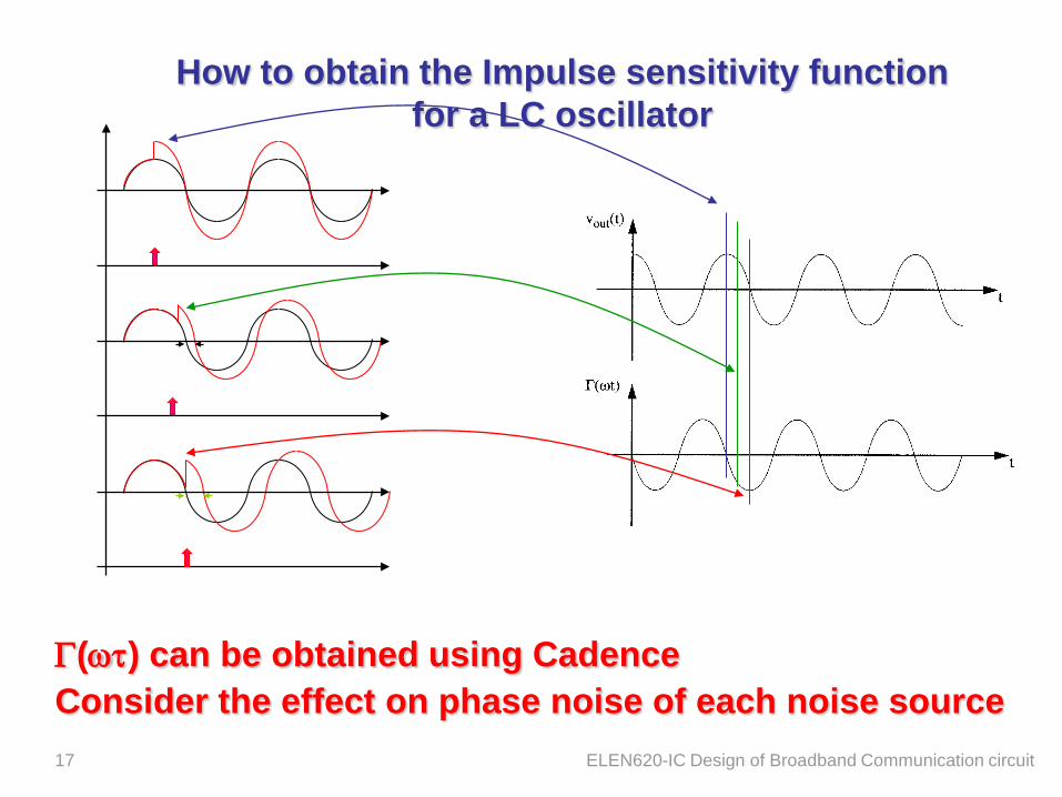
How to obtain the Impulse sensitivity function for a LC oscillator
Γ(ωτ) can be obtained using Cadence Consider the effect on phase noise of each noise source
YCLO
AMSC-TAMU 18
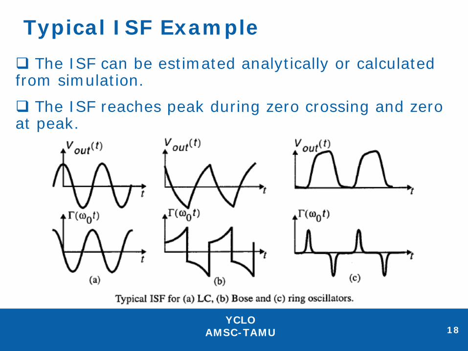
Typical ISF Example The ISF can be estimated analytically or calculated from simulation. The ISF reaches peak during zero crossing and zero at peak.

Phase Noise Computation
19
( ) ( ) ( )
( ) ( ) ( ) ( ) ( ) τττωτττφ
ττωτ
φ
φ
diq
dith
tuq
th
t
o
o
∫∫∞−
∞
∞−
Γ==
−Γ
=
max
max
1,t
function impulse noise phase th thecurrent wi noisearbitrary any
theof integral on)(convolutiion superposit by the computed becan then noise phase The
,
function impulse noise phase obtain the toused isfunction y sensitivit impulse The

ISF Decomposition w/ Fourier Series
20
( ) ( )
( ) ( ) ( ) ( )
ts.coefficien ISF the toaccording scaled and
bandsfrequency different fromdown mixed is noisecurrent they,Essentiall d.deteremine are tscoefficien
Fourier ISF theonce computed be tosource noisearbitrary an from phase excess theallows This
cos2
1t
by computed becan then noise phase The
harmonic. ISFth theof phase theis and real are tscoefficien thewhere
cos2
seriesFourier a as expressed bemay it periodic, is ISF thebecause and insight,further gain order toIn
1
0
max
1
0
+=
++=Γ
∑ ∫∫
∑
∞
= ∞−∞−
∞
=
no
t
n
t
nn
nnono
dnicdicq
nc
ncc
ττωτττφ
θ
θτωτω

Phase Noise Frequency Conversion
21
( ) ( )[ ]
( ) ( )
( ) ( )[ ]
( )
.1 toalproportion ispower that thisNote
4log10
powerth carrier wi about the symmetric sidebands ightedequally we twobe will there,cos
waveformsinusoidal a Assuming .at sidebands equal twoshow willspectrumfrequency resulting The
2sin
other than
termsall fromon contributi negligible a be will thereintegral,n computatio noise phase theperformingWhen
cos
frequencyn oscillatio theof multipleinteger
an near isfrequency osecurrent wh noise sinusoidal a have we wherecase simple aconsider First
2
2
max
max
∆
∆
≈∆
+=
∆±
∆∆
≈
=
∆+=
ω
ωqcIP
tttv
ωqωtcItφ
mn
tmIti
m
mmSBC
oout
mm
om
ω
φω
ω
ωω

Phase Noise Due to White & 1/f Sources
22
( )
.1by weightedand
teddownconver getscarrier theof multiplesinteger higher near noise White there.stayscarrier near the Noise
carrier. near the noise 1 becomes noise 1 so ,t coefficienby weightedd,upconverte gets dcnear Noise
.1by weightedare and itself
carrier near the fold allfrequency carrier theof multiplesinteger near components noise Here
4log10
in results source noise whitea of case general the toanalysis previous theExtending
2
30
2
22max
0
22
f
ffc
ω
ωq
cf
i
P mm
n
SBC
∆
∆∆≈∆
∑∞
=ω
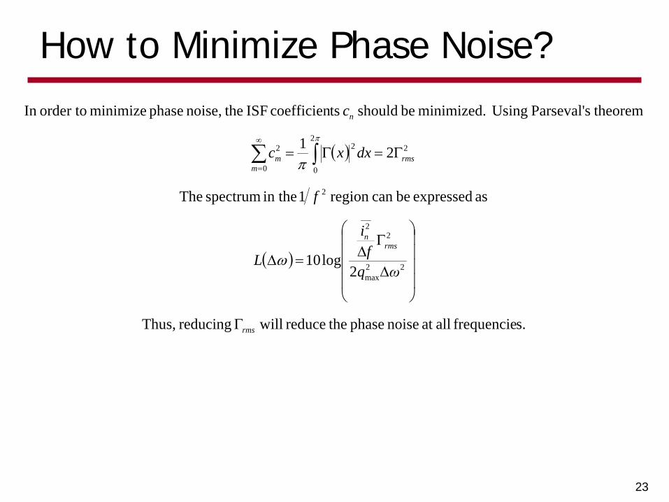
How to Minimize Phase Noise?
23
( )
( )
s.frequencie allat noise phase thereduce will reducing Thus,
2log10
as expressed becan region 1 in the spectrum The
21
theoremsParseval' Usingminimized. be should tscoefficien ISF thenoise, phase minimize order toIn
22max
22
2
2
0
22
0
2
rms
rmsn
rmsm
m
n
ωqf
i
L
f
dxxc
c
Γ
∆
Γ∆=∆
Γ=Γ= ∫∑∞
=
ω
π
π

1/f Corner Frequency
24
( )
noise. 1in reductions dramaticfor potential theis e then thersymmetry, time-fall and -risethrough
minimized is If corner. noisecuit device/cir 1 thelower thangenerally is This
4
isfrequency corner 1 theThus,
8log10
slide previous theFrom
frequencycorner 1 theis where
content 1 includes which noisecurrent Consider
2
12
20
11
3
122
max
20
2
1
1221,
3
f
f
c
f
ωq
cf
i
L
f
ii
f
dc
rms
dcf
rmsff
f
n
f
fnfn
Γ
ΓΓ
=Γ
=∆
∆∆∆=∆
∆=
ωωω
ωω
ω
ω
ωω

Cyclostationary Noise Treatment
25
( ) ( ) ( )
( )
( ) ( ) ( )xxx
x
i
ttiti
n
nn
α
α
ωα
Γ=Γ
=
eff
0
00
ISF effectivean formulate
can we this, Usingunity. of peak value aith function w unitless periodic a is and source, noise
onarycyclostati theof that toequal is peak value whosesource noise whitestationary a is Here
function. periodic a and
noise whitestationary ofproduct theasit gby treatin thishandleeasily can model LTV The
cycle. oscillatoran over ly dramatical changecan noise, thusand current,drain Transistor

Key Oscillator Design Points
26
• As the LTI model predicts, oscillator signal power and Q should be maximized
• Ideally, the energy returned to the tank should be delivered all at once when the ISF is minimum
• Oscillators with symmetry properties that have small Γdc will provide minimum 1/f noise upconversion
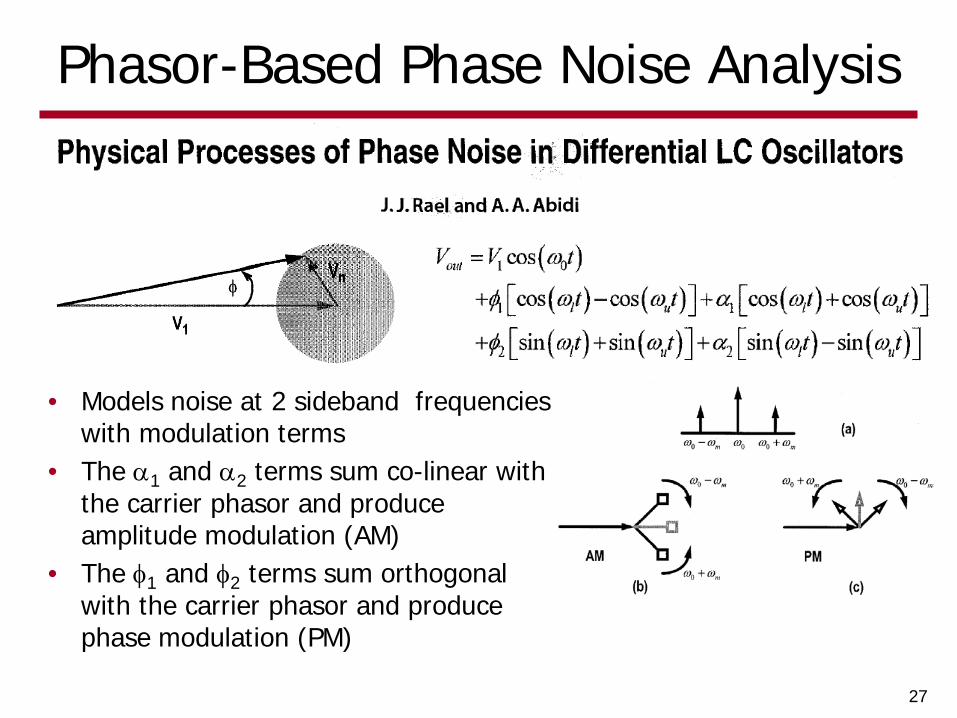
Phasor-Based Phase Noise Analysis
27
• Models noise at 2 sideband frequencies with modulation terms
• The α1 and α2 terms sum co-linear with the carrier phasor and produce amplitude modulation (AM)
• The φ1 and φ2 terms sum orthogonal with the carrier phasor and produce phase modulation (PM)

Phasor-Based LC Oscillator Analysis
28
• This phasor-based approach can be used to find closed-form expressions for LC oscillator phase noise that provide design insight
• In particular, an accurate expression for the Leeson model F parameter is obtained
{ } ( )dBc/Hz 2
2log102
∆
=∆ω
ωωQP
FkTL o
sig

LC Oscillator F Parameter
29
• 1st Term = Tank Resistance Noise • 2nd Term = Cross-Coupled Pair Noise • 3rd Term = Tail Current Source Noise
{ } ( )dBc/Hz 2
2log102
∆
=∆ω
ωωQP
FkTL o
sig
• The above expression gives us insight on how to optimize the oscillator to reduce phase noise
• The tail current source is often a significant contributor to total noise
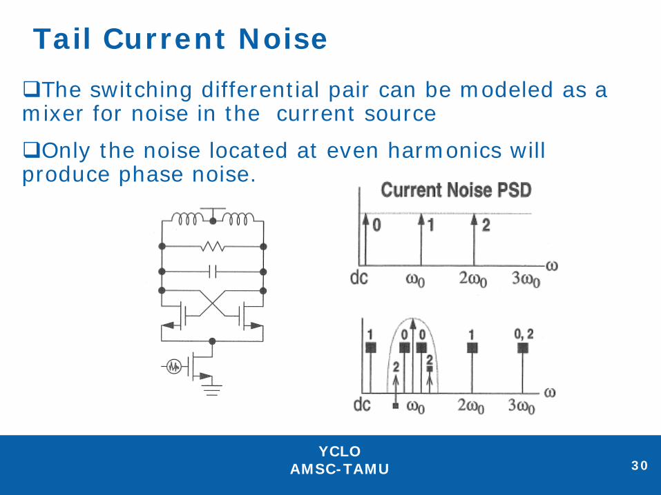
Tail Current Noise The switching differential pair can be modeled as a mixer for noise in the current source Only the noise located at even harmonics will produce phase noise.
YCLO AMSC-TAMU 30

Loading in Current-Biased Oscillator
YCLO AMSC-TAMU 31
• The current source plays 2 roles • It sets the oscillator bias
current • Provides a high impedance
in series with the switching transistors to prevent resonator loading
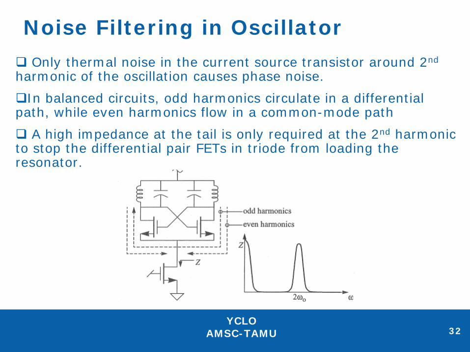
Noise Filtering in Oscillator Only thermal noise in the current source transistor around 2nd harmonic of the oscillation causes phase noise. In balanced circuits, odd harmonics circulate in a differential path, while even harmonics flow in a common-mode path A high impedance at the tail is only required at the 2nd harmonic to stop the differential pair FETs in triode from loading the resonator.
YCLO AMSC-TAMU 32

Noise Filtering in Oscillator Tail-biased VCO with noise filtering.
YCLO AMSC-TAMU 33
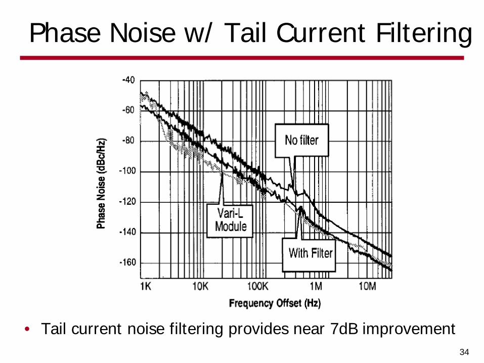
Phase Noise w/ Tail Current Filtering
34
• Tail current noise filtering provides near 7dB improvement

Noise Filtering in Oscillator A top-biased VCO often provides improved substrate noise rejection and reduced flicker noise
YCLO AMSC-TAMU 35

Next Time
• Divider Circuits
36

37 ELEN620-IC Design of Broadband Communication circuit
The input sensitivity function can be characterized as a Fourier Series: An the phase noise is then Therefore:
In general the impulse sensitivity function is periodic with a fundamental frequency equal to the oscillating frequency

38 ELEN620-IC Design of Broadband Communication circuit
Due to the periodicity of the terms, the series converge to (n=m term only): Phase noise
If the input noise is represented as
∆ω
mω0 (m-1)ω0
mω0 ∆ω
Noise
Γ

39 ELEN620-IC Design of Broadband Communication circuit
If the input noise is represented by its power distribution function
For small noise level
( )( )( ) ( ) ( )( )( ) ( )( ) ( )ttsinVtcosVV
tsintsinVtcosVVttcosVV
o0o0out
o0o0out
o0out
φωωφωω
φω
−≅−≅
+=


![ECEN620: Network Theory Broadband Circuit Design Fall 2019ece.tamu.edu/~spalermo/ecen620/lecture07_ee620_vcos.pdf• VCO Jitter 23. Oscillator Noise 24 Jitter [McNeill] Phase Noise](https://img.dokumen.tips/doc/110x75/5eb0f0afdb23476d411ded00/ecen620-network-theory-broadband-circuit-design-fall-spalermoecen620lecture07ee620vcospdf.jpg)


![ECEN620: Network Theory Broadband Circuit Design Fall 2014 · 2020. 10. 30. · Multiphase Clock Generation ... • Sinusoidal • Linear [Bulzacchelli] [Weinlader] 15. DLL Frequency](https://img.dokumen.tips/doc/110x75/60eb74e02337a65b583b6c1e/ecen620-network-theory-broadband-circuit-design-fall-2014-2020-10-30-multiphase.jpg)