Embed Size (px)
Citation preview

Brigham Young University Brigham Young University
BYU ScholarsArchive BYU ScholarsArchive
Theses and Dissertations
2004-07-01
Dynamic Element Matching Techniques For Delta-Sigma ADCs Dynamic Element Matching Techniques For Delta-Sigma ADCs
With Large Internal Quantizers With Large Internal Quantizers
Brent C. Nordick Brigham Young University - Provo
Follow this and additional works at: https://scholarsarchive.byu.edu/etd
Part of the Electrical and Computer Engineering Commons
BYU ScholarsArchive Citation BYU ScholarsArchive Citation Nordick, Brent C., "Dynamic Element Matching Techniques For Delta-Sigma ADCs With Large Internal Quantizers" (2004). Theses and Dissertations. 134. https://scholarsarchive.byu.edu/etd/134
This Thesis is brought to you for free and open access by BYU ScholarsArchive. It has been accepted for inclusion in Theses and Dissertations by an authorized administrator of BYU ScholarsArchive. For more information, please contact [email protected], [email protected].

DYNAMIC ELEMENT MATCHING TECHNIQUES FOR
DELTA-SIGMA ADCS WITH LARGE INTERNAL QUANTIZERS
by
Brent C. Nordick
A thesis submitted to the faculty of
Brigham Young University
in partial fulfillment of the requirements for the degree of
Master of Science
Department of Electrical and Computer Engineering
Brigham Young University
August 2004

Copyright c© 2004 Brent C. Nordick
All Rights Reserved
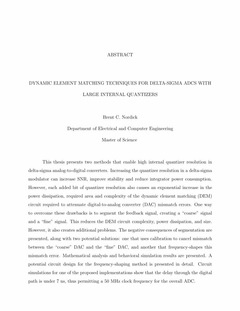
ABSTRACT
DYNAMIC ELEMENT MATCHING TECHNIQUES FOR DELTA-SIGMA ADCS WITH
LARGE INTERNAL QUANTIZERS
Brent C. Nordick
Department of Electrical and Computer Engineering
Master of Science
This thesis presents two methods that enable high internal quantizer resolution in
delta-sigma analog-to-digital converters. Increasing the quantizer resolution in a delta-sigma
modulator can increase SNR, improve stability and reduce integrator power consumption.
However, each added bit of quantizer resolution also causes an exponential increase in the
power dissipation, required area and complexity of the dynamic element matching (DEM)
circuit required to attenuate digital-to-analog converter (DAC) mismatch errors. One way
to overcome these drawbacks is to segment the feedback signal, creating a “coarse” signal
and a “fine” signal. This reduces the DEM circuit complexity, power dissipation, and size.
However, it also creates additional problems. The negative consequences of segmentation are
presented, along with two potential solutions: one that uses calibration to cancel mismatch
between the “coarse” DAC and the “fine” DAC, and another that frequency-shapes this
mismatch error. Mathematical analysis and behavioral simulation results are presented. A
potential circuit design for the frequency-shaping method is presented in detail. Circuit
simulations for one of the proposed implementations show that the delay through the digital
path is under 7 ns, thus permitting a 50 MHz clock frequency for the overall ADC.

ACKNOWLEDGMENTS
I would like to gratefully acknowledge the support and encouragement from my wife,
Andrea. To her go the official titles of “Tech Writer” and “Hyphenation-Queen” for all the
proofreading and grammar checking. (Any mistakes still present in this text are most likely
because I made some changes and didn’t ask her to check them over.)
Special thanks to my wonderful parents for their support, and for providing a roof
over our heads for a bit when it was needed. Thanks as well to my brothers and sisters for
their examples in striving for advanced degrees.
I would like to acknowledge Dr. Craig Petrie for the time he has taken to proofread
and suggest improvements for the various drafts of this thesis. I also acknowledge the other
two members of my graduate committee, Dr. Michael Rice and Dr. Brent Nelson, for their
help with my thesis. Special thanks to all three for the instruction and mentoring they have
provided during my time as a student at BYU.
I would like to thank the Electrical Engineering Department of BYU: the combination
of wonderful professors, staff, and laboratory facilities made all the difference. (Additional
thanks for the LATEX thesis style package they provided.)
Special thanks to the Intel Research Council for funding this research.
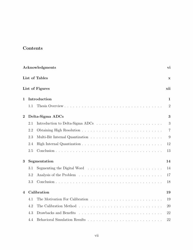
Contents
Acknowledgments vi
List of Tables x
List of Figures xii
1 Introduction 1
1.1 Thesis Overview . . . . . . . . . . . . . . . . . . . . . . . . . . . . . . . . . . 2
2 Delta-Sigma ADCs 3
2.1 Introduction to Delta-Sigma ADCs . . . . . . . . . . . . . . . . . . . . . . . 3
2.2 Obtaining High Resolution . . . . . . . . . . . . . . . . . . . . . . . . . . . . 7
2.3 Multi-Bit Internal Quantization . . . . . . . . . . . . . . . . . . . . . . . . . 9
2.4 High Internal Quantization . . . . . . . . . . . . . . . . . . . . . . . . . . . . 12
2.5 Conclusion . . . . . . . . . . . . . . . . . . . . . . . . . . . . . . . . . . . . . 13
3 Segmentation 14
3.1 Segmenting the Digital Word . . . . . . . . . . . . . . . . . . . . . . . . . . 14
3.2 Analysis of the Problem . . . . . . . . . . . . . . . . . . . . . . . . . . . . . 17
3.3 Conclusion . . . . . . . . . . . . . . . . . . . . . . . . . . . . . . . . . . . . . 18
4 Calibration 19
4.1 The Motivation For Calibration . . . . . . . . . . . . . . . . . . . . . . . . . 19
4.2 The Calibration Method . . . . . . . . . . . . . . . . . . . . . . . . . . . . . 20
4.3 Drawbacks and Benefits . . . . . . . . . . . . . . . . . . . . . . . . . . . . . 22
4.4 Behavioral Simulation Results . . . . . . . . . . . . . . . . . . . . . . . . . . 22
vii

4.5 Conclusion . . . . . . . . . . . . . . . . . . . . . . . . . . . . . . . . . . . . . 23
5 Requantization 25
5.1 The Noise-Shaped Requantization (ReQ) Method . . . . . . . . . . . . . . . 25
5.2 Drawbacks and Benefits . . . . . . . . . . . . . . . . . . . . . . . . . . . . . 27
5.3 Behavioral Circuit Simulation Results . . . . . . . . . . . . . . . . . . . . . . 31
5.4 Conclusion . . . . . . . . . . . . . . . . . . . . . . . . . . . . . . . . . . . . . 31
6 Circuit Design 33
6.1 Circuit Overviews . . . . . . . . . . . . . . . . . . . . . . . . . . . . . . . . . 33
6.1.1 Encoder . . . . . . . . . . . . . . . . . . . . . . . . . . . . . . . . . . 33
6.1.2 ReQ Block . . . . . . . . . . . . . . . . . . . . . . . . . . . . . . . . . 34
6.1.3 Decode Logic . . . . . . . . . . . . . . . . . . . . . . . . . . . . . . . 38
6.1.4 DEM Logic . . . . . . . . . . . . . . . . . . . . . . . . . . . . . . . . 38
6.2 Circuit Simulations . . . . . . . . . . . . . . . . . . . . . . . . . . . . . . . . 45
6.3 Conclusion . . . . . . . . . . . . . . . . . . . . . . . . . . . . . . . . . . . . . 47
7 Conclusion 53
7.1 Contributions . . . . . . . . . . . . . . . . . . . . . . . . . . . . . . . . . . . 53
7.2 Summary of Results . . . . . . . . . . . . . . . . . . . . . . . . . . . . . . . 53
7.3 Areas for Potential Future Research . . . . . . . . . . . . . . . . . . . . . . . 54
A Complete Circuit Schematics 57
A.1 Top Level Schematic . . . . . . . . . . . . . . . . . . . . . . . . . . . . . . . 57
A.2 Bubble Decode . . . . . . . . . . . . . . . . . . . . . . . . . . . . . . . . . . 58
A.2.1 Inverter . . . . . . . . . . . . . . . . . . . . . . . . . . . . . . . . . . 59
A.2.2 3 Input Nor . . . . . . . . . . . . . . . . . . . . . . . . . . . . . . . . 60
A.3 2’s Complement Encoder . . . . . . . . . . . . . . . . . . . . . . . . . . . . . 61
A.4 Unsigned Encoder . . . . . . . . . . . . . . . . . . . . . . . . . . . . . . . . . 62
A.5 ReQ . . . . . . . . . . . . . . . . . . . . . . . . . . . . . . . . . . . . . . . . 63
A.5.1 8-bit Subtractor . . . . . . . . . . . . . . . . . . . . . . . . . . . . . . 64
A.5.2 Full Adder . . . . . . . . . . . . . . . . . . . . . . . . . . . . . . . . . 65
viii
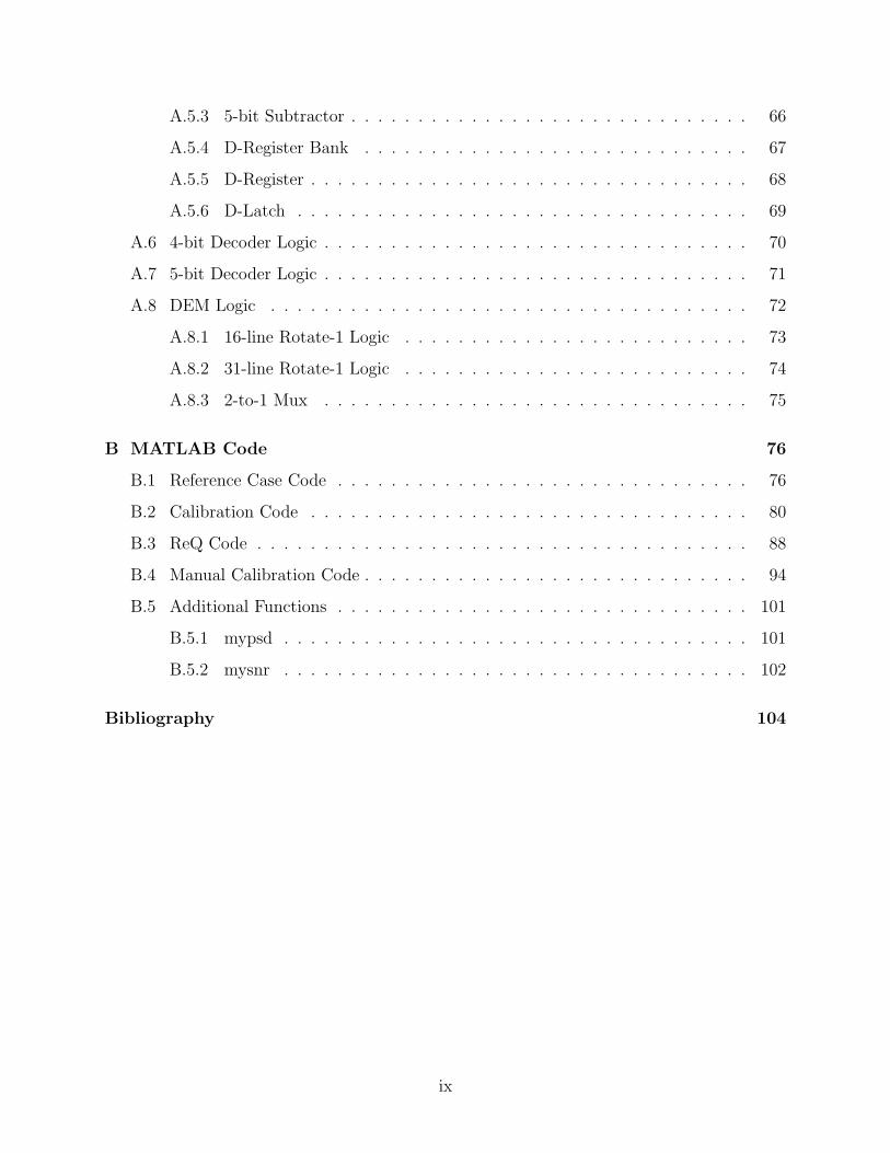
A.5.3 5-bit Subtractor . . . . . . . . . . . . . . . . . . . . . . . . . . . . . . 66
A.5.4 D-Register Bank . . . . . . . . . . . . . . . . . . . . . . . . . . . . . 67
A.5.5 D-Register . . . . . . . . . . . . . . . . . . . . . . . . . . . . . . . . . 68
A.5.6 D-Latch . . . . . . . . . . . . . . . . . . . . . . . . . . . . . . . . . . 69
A.6 4-bit Decoder Logic . . . . . . . . . . . . . . . . . . . . . . . . . . . . . . . . 70
A.7 5-bit Decoder Logic . . . . . . . . . . . . . . . . . . . . . . . . . . . . . . . . 71
A.8 DEM Logic . . . . . . . . . . . . . . . . . . . . . . . . . . . . . . . . . . . . 72
A.8.1 16-line Rotate-1 Logic . . . . . . . . . . . . . . . . . . . . . . . . . . 73
A.8.2 31-line Rotate-1 Logic . . . . . . . . . . . . . . . . . . . . . . . . . . 74
A.8.3 2-to-1 Mux . . . . . . . . . . . . . . . . . . . . . . . . . . . . . . . . 75
B MATLAB Code 76
B.1 Reference Case Code . . . . . . . . . . . . . . . . . . . . . . . . . . . . . . . 76
B.2 Calibration Code . . . . . . . . . . . . . . . . . . . . . . . . . . . . . . . . . 80
B.3 ReQ Code . . . . . . . . . . . . . . . . . . . . . . . . . . . . . . . . . . . . . 88
B.4 Manual Calibration Code . . . . . . . . . . . . . . . . . . . . . . . . . . . . . 94
B.5 Additional Functions . . . . . . . . . . . . . . . . . . . . . . . . . . . . . . . 101
B.5.1 mypsd . . . . . . . . . . . . . . . . . . . . . . . . . . . . . . . . . . . 101
B.5.2 mysnr . . . . . . . . . . . . . . . . . . . . . . . . . . . . . . . . . . . 102
Bibliography 104
ix
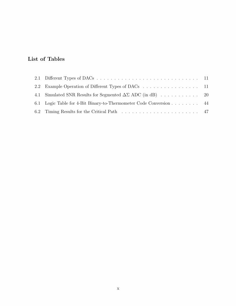
List of Tables
2.1 Different Types of DACs . . . . . . . . . . . . . . . . . . . . . . . . . . . . . 11
2.2 Example Operation of Different Types of DACs . . . . . . . . . . . . . . . . 11
4.1 Simulated SNR Results for Segmented ∆Σ ADC (in dB) . . . . . . . . . . . 20
6.1 Logic Table for 4-Bit Binary-to-Thermometer Code Conversion . . . . . . . . 44
6.2 Timing Results for the Critical Path . . . . . . . . . . . . . . . . . . . . . . 47
x
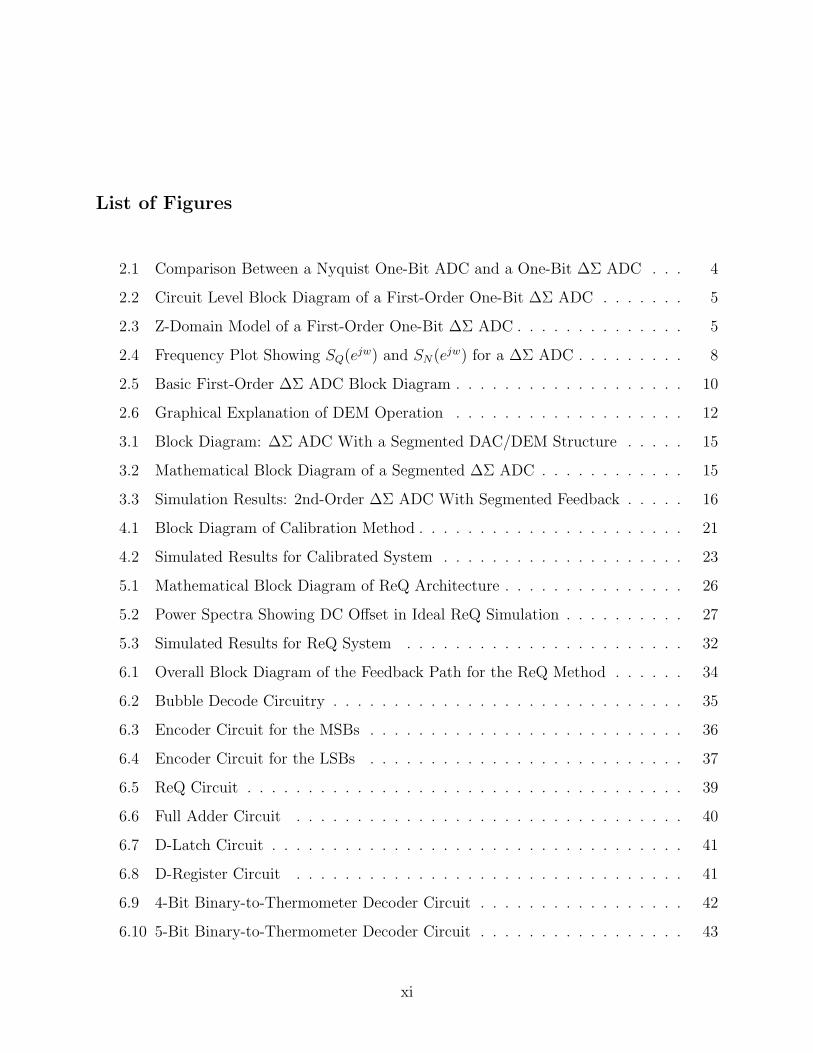
List of Figures
2.1 Comparison Between a Nyquist One-Bit ADC and a One-Bit ∆Σ ADC . . . 4
2.2 Circuit Level Block Diagram of a First-Order One-Bit ∆Σ ADC . . . . . . . 5
2.3 Z-Domain Model of a First-Order One-Bit ∆Σ ADC . . . . . . . . . . . . . . 5
2.4 Frequency Plot Showing SQ(ejw) and SN(ejw) for a ∆Σ ADC . . . . . . . . . 8
2.5 Basic First-Order ∆Σ ADC Block Diagram . . . . . . . . . . . . . . . . . . . 10
2.6 Graphical Explanation of DEM Operation . . . . . . . . . . . . . . . . . . . 12
3.1 Block Diagram: ∆Σ ADC With a Segmented DAC/DEM Structure . . . . . 15
3.2 Mathematical Block Diagram of a Segmented ∆Σ ADC . . . . . . . . . . . . 15
3.3 Simulation Results: 2nd-Order ∆Σ ADC With Segmented Feedback . . . . . 16
4.1 Block Diagram of Calibration Method . . . . . . . . . . . . . . . . . . . . . . 21
4.2 Simulated Results for Calibrated System . . . . . . . . . . . . . . . . . . . . 23
5.1 Mathematical Block Diagram of ReQ Architecture . . . . . . . . . . . . . . . 26
5.2 Power Spectra Showing DC Offset in Ideal ReQ Simulation . . . . . . . . . . 27
5.3 Simulated Results for ReQ System . . . . . . . . . . . . . . . . . . . . . . . 32
6.1 Overall Block Diagram of the Feedback Path for the ReQ Method . . . . . . 34
6.2 Bubble Decode Circuitry . . . . . . . . . . . . . . . . . . . . . . . . . . . . . 35
6.3 Encoder Circuit for the MSBs . . . . . . . . . . . . . . . . . . . . . . . . . . 36
6.4 Encoder Circuit for the LSBs . . . . . . . . . . . . . . . . . . . . . . . . . . 37
6.5 ReQ Circuit . . . . . . . . . . . . . . . . . . . . . . . . . . . . . . . . . . . . 39
6.6 Full Adder Circuit . . . . . . . . . . . . . . . . . . . . . . . . . . . . . . . . 40
6.7 D-Latch Circuit . . . . . . . . . . . . . . . . . . . . . . . . . . . . . . . . . . 41
6.8 D-Register Circuit . . . . . . . . . . . . . . . . . . . . . . . . . . . . . . . . 41
6.9 4-Bit Binary-to-Thermometer Decoder Circuit . . . . . . . . . . . . . . . . . 42
6.10 5-Bit Binary-to-Thermometer Decoder Circuit . . . . . . . . . . . . . . . . . 43
xi

6.11 Block Diagram of DEM Circuitry . . . . . . . . . . . . . . . . . . . . . . . . 45
6.12 DEM Circuitry . . . . . . . . . . . . . . . . . . . . . . . . . . . . . . . . . . 46
6.13 Timing Simulation for ReQ Bubble Decode Block . . . . . . . . . . . . . . . 48
6.14 Timing Simulation for ReQ Encoder Block . . . . . . . . . . . . . . . . . . . 49
6.15 Timing Simulation for ReQ 8-bit Subtractor Block . . . . . . . . . . . . . . . 50
6.16 Timing Simulation for ReQ 5-bit Subtractor Block . . . . . . . . . . . . . . . 51
6.17 Timing Simulation for ReQ Decoder Block . . . . . . . . . . . . . . . . . . . 52
A.1 Overall Schematic for Digital Feedback Path . . . . . . . . . . . . . . . . . . 57
A.2 Bubble Decode Logic . . . . . . . . . . . . . . . . . . . . . . . . . . . . . . . 58
A.3 Inverter . . . . . . . . . . . . . . . . . . . . . . . . . . . . . . . . . . . . . . 59
A.4 Nor Gate . . . . . . . . . . . . . . . . . . . . . . . . . . . . . . . . . . . . . 60
A.5 2’s Complement Encoder . . . . . . . . . . . . . . . . . . . . . . . . . . . . . 61
A.6 Unsigned Encoder . . . . . . . . . . . . . . . . . . . . . . . . . . . . . . . . . 62
A.7 Requantization Logic . . . . . . . . . . . . . . . . . . . . . . . . . . . . . . . 63
A.8 8-bit Subtractor . . . . . . . . . . . . . . . . . . . . . . . . . . . . . . . . . . 64
A.9 Full Adder Design . . . . . . . . . . . . . . . . . . . . . . . . . . . . . . . . . 65
A.10 5-bit Subtractor . . . . . . . . . . . . . . . . . . . . . . . . . . . . . . . . . . 66
A.11 D-Register Bank . . . . . . . . . . . . . . . . . . . . . . . . . . . . . . . . . 67
A.12 D-Register . . . . . . . . . . . . . . . . . . . . . . . . . . . . . . . . . . . . . 68
A.13 D-Latch . . . . . . . . . . . . . . . . . . . . . . . . . . . . . . . . . . . . . . 69
A.14 4-bit Binary-to-Thermometer Code Decoder . . . . . . . . . . . . . . . . . . 70
A.15 5-bit Binary-to-Thermometer Code Decoder . . . . . . . . . . . . . . . . . . 71
A.16 Dynamic Element Matching Logic . . . . . . . . . . . . . . . . . . . . . . . . 72
A.17 16-Input Rotate-1 . . . . . . . . . . . . . . . . . . . . . . . . . . . . . . . . . 73
A.18 31-Input Rotate-1 . . . . . . . . . . . . . . . . . . . . . . . . . . . . . . . . . 74
A.19 2-to-1 Mux . . . . . . . . . . . . . . . . . . . . . . . . . . . . . . . . . . . . 75
xii

Chapter 1
Introduction
The analog-to-digital converter (ADC) is the essential link between “real world” ana-
log signals and digital electronics. In the current digital age, they are nearly everywhere:
car sensors, home thermostats, DVD and CD players, televisions, personal computers, cell
phones, and many other common devices. As consumers expect more and more from digital
electronic devices, faster ADCs with higher resolution are needed. At the same time, cell
phones and other “mobile” technologies are demanding lower power alternatives. As such,
improving present ADC architectures is an active field of research.
The delta-sigma (∆Σ) ADC is one architecture that is being examined for use in low-
power, high-resolution, moderate-speed applications. Conventionally, ∆Σ ADCs are used
for low-frequency applications (< 100 kHz) requiring high resolution (> 14 bits), such as
digital audio or high-precision instrumentation [1, 2, 3]. Recent work, however, is extending
the signal bandwidths of ∆Σ ADCs into the MHz range while maintaining high resolution
[4, 5].
One method of extending the signal bandwidth of a ∆Σ ADC without decreasing the
resolution is to appropriately trade off internal quantization and oversampling ratio. As the
oversampling ratio is reduced, the signal bandwidth increases, but the signal-to-noise ratio
(resolution) is decreased. This can be recovered by increasing the number of bits in the
internal quantization path. Several problems arise from this approach. This thesis presents
an analysis of these problems and two potential solutions. Simulations show that near-ideal
resolution can be maintained for practical implementations.
1
1.1 Thesis Overview
The thesis begins with a short introduction of ∆Σ ADCs (Chapter 2). Some of the
issues involved in designing high-speed, high-resolution ADCs are presented. Increasing the
resolution of the internal quantization is shown to be a desirable step for higher bandwidth
design, and accompanying problems for quantization levels above one bit are discussed.
Problems that occur when internal quantization levels are increased too far are covered, and
a potential solution is presented: segmentation.
In Chapter 3, the proposed method of segmentation is described, along with its inher-
ent drawbacks. The method is analyzed, and the source of the main drawback is identified.
In Chapter 4, calibration is presented as a potential solution to the problems asso-
ciated with segmentation. A mathematical analysis is provided. An in-depth description
of how to implement the calibration solution is presented, along with the potential benefits
and drawbacks. Behavioral simulations are provided to demonstrate the performance of this
solution.
In Chapter 5, another potential solution is presented, this one adapting a method of
selecting the coarse and fine bits developed for ∆Σ DACs [6]. Again, a mathematical analysis
of this solution is presented. A description of the required hardware and its operation is
provided, again with the potential benefits and drawbacks. Simulation results are shown to
demonstrate this solution’s performance.
In Chapter 6, circuits implementing the ReQ method are presented, with schematics
and explanations. SPICE simulations are presented showing the worst-case timing of the
design, verifying that it is fast enough to meet the design constraints.
As a conclusion, Chapter 7 reviews the research presented and then compares the
results of the two potential solutions and their respective strengths and weaknesses. Contri-
butions of this project are presented, and areas for continued research are proposed.
2
Chapter 2
Delta-Sigma ADCs
As a starting point for discussion, this chapter presents the key operating principles of
∆Σ ADCs. The design parameters which can be adjusted to increase the output resolution
are presented, as well as the practical limits of their application.
2.1 Introduction to Delta-Sigma ADCs
This is not meant to be a full tutorial on ∆Σ ADCs, but a basic summary of key
concepts to provide a common basis for further discussion. As presented in [1], a ∆Σ ADC
achieves high resolution by trading resolution in time for resolution in amplitude. The
internal circuitry of the ADC is clocked at some multiple of the required external data
rate (the oversampling ratio), providing multiple internal data points that can be digitally
processed to provide an output of much higher resolution than could be otherwise obtained.
The effective bandwidth is limited, however, to a fraction of the achievable internal frequency.
Three of the key design parameters that affect the resolution of a ∆Σ ADC are:
The oversampling ratio (OSR), the modulator order (L in the following equations), and the
number of bits of internal quantization (N). Each of these will be discussed in more depth
in Section 2.2.
Figure 2.1 shows how a ∆Σ ADC works in comparison with a “standard” (non-
oversampling or “Nyquist”) ADC architecture. Simple one-bit ADCs are used for the com-
parison, meaning that each ADC output is quantized to a single bit. The first part of the
picture shows the operation of a Nyquist ADC. The dashed line is the input to the ADC, and
the circles represent ADC outputs. The one-bit ADC is very inaccurate in its representation
of the input signal, since there are only two possible levels for the outputs: low and high.
3

0 10 20 30 40 50 60 70 80
−1
−0.5
0
0.5
1
Am
plitu
de
One−bit Nyquist ADC
InputDigital Output
0 10 20 30 40 50 60 70 80
−1
−0.5
0
0.5
1
Time
Am
plitu
de
One−bit delta−sigma ADC
InputIntermediate ValuesDigital Output
Figure 2.1: Comparison Between a Nyquist One-Bit ADC and a One-Bit ∆Σ ADC
The lower portion of the figure shows the operation of a one-bit ∆Σ converter. The input
signal is the same, but the ∆Σ device generates ten intermediate values for each output.
These intermediate values are filtered to give more precise outputs. From the plot we can
see seven distinct output levels, suggesting that the one-bit ADC could have an output that
has at least three bits of accuracy.
Figure 2.2 shows the circuit-level block diagram of a basic, first-order ∆Σ ADC, and
Figure 2.3 shows its equivalent z-domain model. From these it can be shown that:
Y (z) = z−1X(z) +(1− z−1
)Q(z). (2.1)
It can also be shown that the noise transfer function from Q(z) to the output is:
Y (z)
Q(z)=(1− z−1
). (2.2)
Given that q(n) (the time domain representation of the signal Q(z)) is the quantiza-
tion noise inserted by the internal quantizer, it is limited in magnitude to one-half an LSB
4
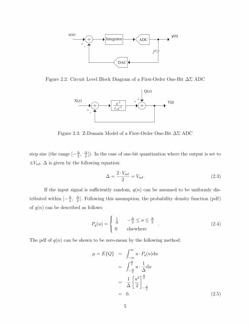
x(n)
DAC
+
2N
ADC-
Integratory(n)
Figure 2.2: Circuit Level Block Diagram of a First-Order One-Bit ∆Σ ADC
X(z)
+ -
z-1
1-z-1Y(z)
Q(z)
+ +
Figure 2.3: Z-Domain Model of a First-Order One-Bit ∆Σ ADC
step size (the range [−∆2, ∆
2]). In the case of one-bit quantization where the output is set to
±Vref, ∆ is given by the following equation:
∆ =2 ·Vref
2= Vref . (2.3)
If the input signal is sufficiently random, q(n) can be assumed to be uniformly dis-
tributed within [−∆2, ∆
2]. Following this assumption, the probability density function (pdf)
of q(n) can be described as follows:
Pq(u) =
1∆
−∆2≤ u ≤ ∆
2
0 elsewhere. (2.4)
The pdf of q(n) can be shown to be zero-mean by the following method:
µ = E{Q} =∫ ∞
−∞u ·Pq(u)du
=∫ ∆
2
−∆2
u · 1
∆du
=1
∆
[u2
2
]∆2
−∆2
= 0. (2.5)
5

Following a similar process, the variance of q(n) can be shown to be a constant:
σ2 = E{Q2} =∫ ∞
−∞u2 ·Pq(u)du
=∫ ∆
2
−∆2
u2 · 1
∆du
=1
∆
[u3
3
]∆2
−∆2
=∆2
12. (2.6)
The quantization noise sequence is usually modeled as a “wide-sense stationary”
(WSS) random process [7]. The power spectral density (PSD) of a WSS random process
is defined as the discrete-time Fourier transform (DTFT) of the autocorrelation function.
Given that the signal is zero-mean, this is equal to the covariance:
SQ(ejω) = σ2. (2.7)
Notice that the power is not a function of frequency; it is equal at all frequencies. This PSD
characterizes the quantization noise added to the samples by the ∆Σ ADC, and the noise
defines the accuracy, or SNR (signal-to-noise ratio), of the internal quantizer.
However, in the case of a ∆Σ ADC, the quantization error is not directly transmitted
to the output, but is shaped by the (1− z−1) term in Equation (2.2). The modulation noise,
or the quantization noise’s effect on the output, can be shown to be:
N(z) =(1− z−1
)Q(z). (2.8)
The PSD of the shaped noise is then:
SN(ejω) =∣∣∣1− ejω
∣∣∣σ2
=(1− ejω
) (1 + ejω
)σ2
= [2− 2 cos(ω)] σ2. (2.9)
The modulation noise power is a function of frequency, as shown by Equation (2.9).
A ∆Σ ADC is only interested in a small portion of the signal band, so the modulation noise
power in the band of interest is given by:
S∆Σ(ejω) =1
2π
∫ ω0
−ω0
SN(ejω)dω
6
=σ2
2π
∫ ω0
−ω0
[2− 2 cos(ω)]dω
=2σ2
π[ω0 − sin(ω0)]
≈ 2σ2
π
[ω0 − ω0 +
ω3
6
]
≈ σ2ω3
3π(2.10)
Given that ω0 = ωs/(2 ·OSR) and that ωs = 2π, Equation (2.10) can be rewritten as
follows:
S∆Σ(ejω) ≈ σ2 · 1
3π·ω3
0
≈(
Vref√12
)2
· 1
3π· π3
OSR3
≈(
Vref√12
)2
· π2
3· 1
OSR3 (2.11)
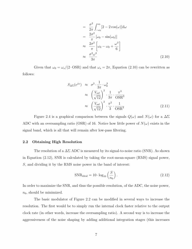
Figure 2.4 is a graphical comparison between the signals Q(ω) and N(ω) for a ∆Σ
ADC with an oversampling ratio (OSR) of 16. Notice how little power of N(ω) exists in the
signal band, which is all that will remain after low-pass filtering.
2.2 Obtaining High Resolution
The resolution of a ∆Σ ADC is measured by its signal-to-noise ratio (SNR). As shown
in Equation (2.12), SNR is calculated by taking the root-mean-square (RMS) signal power,
S, and dividing it by the RMS noise power in the band of interest:
SNRideal = 10 · log10
(S
n0
). (2.12)
In order to maximize the SNR, and thus the possible resolution, of the ADC, the noise power,
n0, should be minimized.
The basic modulator of Figure 2.2 can be modified in several ways to increase the
resolution. The first would be to simply run the internal clock faster relative to the output
clock rate (in other words, increase the oversampling ratio). A second way is to increase the
aggressiveness of the noise shaping by adding additional integration stages (this increases
7
10−1
100
−30
−25
−20
−15
−10
−5
0
5
Quantization Error
SQ
(ejω)
Modulation Noise
SN(ejω)
Signal Band
Frequency
Noi
se P
ower
(dB
)
Figure 2.4: Frequency Plot Showing SQ(ejw) and SN(ejw) for a First-Order ∆Σ ADC Withan OSR of 16.
the modulator order). A third method is to increase the number of bits used in the feedback
path, N .
Equation (2.11) can be generalized to give an approximation of the ideal quantization
noise in a ∆Σ ADC:
n0 ≈2 ·Vref
2N√
12· πL
√2L + 1
· 1
OSR(L+0.5). (2.13)
(It should be noted that this derivation assumes that the ∆Σ ADC is using (1− z−1)L noise
shaping. Other noise transfer functions are possible.) This equation is comprised of the
three aforementioned parameters: oversampling ratio (OSR); modulator order, L; and the
number of bits of internal quantization, N . As each is increased, the ideal resolution of the
ADC is increased because the overall noise signal is reduced. However, an increase in any of
the three can also adversely affect power dissipation, design complexity, area required, and
system stability.
8

The OSR is the ratio of how fast the internal digital circuitry must run (sampling
frequency, fs) compared to the Nyquist rate (2fo):
OSR =fs
2fo
=1
2foT. (2.14)
The higher the OSR, the more aggressive the digital filtering (lower cutoff frequency) that
can be done to remove more of the noise, and thus the higher the potential output resolution.
However, increasing the OSR can only be done by either increasing the internal modulator
frequency (which is limited by realizable device speeds), or decreasing the output bandwidth.
For designs requiring high bandwidths, the OSR is limited to relatively small numbers.
The modulator order is generally the number of integration stages in the analog for-
ward path of the ∆Σ ADC. Increasing the modulator order will increase the ADC resolution,
but at the cost of more circuitry. This leads to a more complex design that requires more
power and more chip area. Higher-order modulators are also more difficult to make stable,
which sacrifices some of the aggressiveness of the noise shaping.
The internal quantization level is the number of bits of resolution the internal quan-
tizer uses. The previous discussions in Section 2.1 used one-bit internal quantization. More
internal quantization levels provide an increased resolution to the internal data points, re-
sulting in higher overall resolution. It can also improve the overall system stability. However,
this causes the internal quantizer to become more complex, increasing the chip area and re-
quired power. Perhaps more importantly, any quantization above one bit requires a DAC
which must be as accurate as the overall ADC, as discussed in Section 2.3. For this reason,
traditional ∆Σ modulators have used strictly two-level (one-bit) internal quantization.
2.3 Multi-Bit Internal Quantization
The problem with internal quantization greater than one bit is caused by the digital-
to-analog conversion required in the ∆Σ modulator feedback path. As shown in Figure 2.5,
the ADC output code passes through a DAC and then is summed into the analog forward
path of the modulator. Any errors introduced by this DAC are added directly to the input
signal and are then transmitted directly to the output along with the input. Because of this,
the feedback DAC must have a resolution equal to the overall required ADC resolution. This
9

Input
DAC
Output
+
2N
ADC DigitalLow Pass Filter-
Integrator
Figure 2.5: Basic First-Order ∆Σ ADC Block Diagram
is easily done for one-bit DACs, which have inherently perfect linearity. However, multi-bit
DACs have various internal element mismatches which prevent them from realizing such high
resolutions given achievable matching in typical VLSI fabrication processes.
This problem is overcome by various noise-shaping algorithms generally known as
“dynamic element matching” (DEM) techniques. DEM algorithms operate on the signal at
the input to the DAC, and take advantage of the oversampling inherent in ∆Σ devices and
attempt to shape the noise generated by the DAC, shifting the noise to frequencies that are
out of the band of interest. The low-pass filter present at the output of the ∆Σ modulator
will then remove this error. DEM noise shaping is similar to ∆Σ noise shaping. However,
DEM is done digitally where the ∆Σ noise shaping discussed earlier is analog, and DEM
operates on noise generated from DAC element mismatches, while ∆Σ noise shaping operates
on the quantization noise.
To understand DEM, the various DAC architectures must be described. Table 2.1
shows the three main categories of interest for this discussion. “Binary-weighted” DACs
have one element for each of the input bits. A 4-bit DAC would have exactly four elements,
each weighted according to the binary place value of each bit: 1:2:4:8. A “unit-element”
or “thermometer-coded” DAC has as many elements as it has input codes (minus one): a
4-bit unit-element DAC would have 24−1 = 15 elements, all weighted equally. “Segmented”
DACs are a split between binary-weighted and unit-element DACs. A 4-bit segmented DAC
may have the two least significant bits realized by 22−1 = 3 elements, of weight “1”, and the
two most significant bits realized by 3 elements of weight “4”. Table 2.2 shows how various
input codes would be realized by a 4-bit DAC from each category.
10
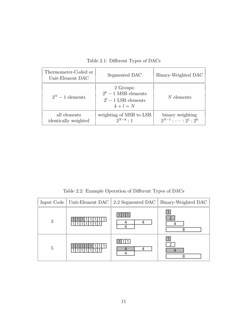
Table 2.1: Different Types of DACs
Thermometer-Coded or
Unit-Element DACSegmented DAC Binary-Weighted DAC
2 Groups:2k − 1 MSB elements
2N − 1 elements2l − 1 LSB elements
N elements
k + l = N
all elements weighting of MSB to LSB binary weightingidentically weighted 2N−k : 1 2N−1 : · · · : 21 : 20
Table 2.2: Example Operation of Different Types of DACs
Input Code Unit-Element DAC 2-2 Segmented DAC Binary-Weighted DAC
3 1 1 1 1 1 1 1 11 1 1 1 1 1 1
1
4
1 1
44
12
48
5 1 1 1 1 1 1 1 11 1 1 1 1 1 1
1
4
1 1
44
12
48
11

1 1 1 1 1 1 1 11 1 1 1 1 1 1
1 1 1 1 1 1 1 11 1 1 1 1 1 1
1 1 1 1 1 1 1 11 1 1 1 1 1 1
Input Code = 2 Input Code = 3 Input Code = 5
Figure 2.6: Graphical Explanation of DEM Operation
DEM algorithms generally use unit-element DACs. Each element of the DAC is
designed to be exactly the same size, but there is always some mismatch present. Standard
unit-element DACs have a fixed error for a given input code because the same unit elements
are used each time to form that code. A code of “1” will be formed with the first unit
element, while a code of “4” would use the first four unit elements. DEM changes the
element selection process, using different unit elements to form the same code in order to
create a time-varying error.
There are several different DEM algorithms, varying mostly in how they choose which
unit elements to use. The method chosen for this research is a data-weighted averaging
(DWA) method, also referred to as barrel-shifting. This method keeps track of the last
element used in the previous code, and uses the next group of elements sequentially. Figure
2.6 demonstrates how this works. For a code of “2” followed by a code of “3” and a code
of “5”, the algorithm would use the first two unit elements in the DAC for the first code,
followed by elements three through five for the second code. The subsequent code would
then begin at the sixth element. This selection method turns each element on and off rapidly.
The end result is that the DAC error is first-order noise shaped with most of the noise power
at higher frequencies, as shown in [8, 9].
2.4 High Internal Quantization
While such DEM algorithms work well for relatively low quantization levels (two to
five bits), they begin to present significant problems when internal quantization levels are
extended farther. Each additional bit of internal quantization causes an exponential increase
in the complexity, size, and power dissipation of the DEM logic and DAC. This is because
DEM algorithms work with unit-element DACs. The DAC must have 2N−1 elements (where
12
N is the number of bits of internal quantization), and the DEM logic must deal with the
control signals feeding those 2N − 1 unit elements.
Increasing the internal quantization level also increases the size, complexity, and
power usage of the internal quantizer. Fortunately, there are some architectures available
that will reduce these effects, two of which are folding and two-step ADC architectures. These
both generate the digital word in two parts, a “coarse” resolution and a “fine” resolution,
allowing the internal quantizer to be smaller and use less power. The drawback of these
architectures is that the time required to perform the quantization increases, potentially
destabilizing the ∆Σ modulator. A folding ADC, with its lower latency, would be the first
obvious choice. Recent research has also shown that it is possible to incorporate two-step
ADCs within a single-loop modulator, potentially maintaining loop stability [10, 11].
Efficient DEM algorithms are needed to accommodate the high level of quantization
achieved with folding, two-step, or other coarse/fine quantizers. Research has shown that
DEM algorithms based on a tree structure can be adapted for use with a segmented DAC
structure [12]. An approach was desired, however, that utilizes the DWA (barrel-shifting)
DEM method in search of a potentially simpler solution.
2.5 Conclusion
The tradeoffs involved in achieving high resolution in ∆Σ ADCs usually lead to low
internal quantization levels and high oversampling rates. In order to achieve higher band-
widths, the OSR needs to be lowered and the internal quantization level increased. New
DEM algorithms are needed to enable internal quantization levels over 5 or 6 bits while
keeping chip size and power dissipation within reasonable bounds.
13
Chapter 3
Segmentation
Technological advancement is always calling for faster, higher resolution ADCs. In
order to have both high bandwidth and high resolution in ∆Σ ADCs, an efficient DEM
algorithm is required to insure the accuracy of the ADC feedback path. This chapter presents
one potential method of achieving such an efficient DEM application.
3.1 Segmenting the Digital Word
As mentioned in Section 2.4, a folding or two-step architecture for the internal quan-
tizer can solve some of the problems arising from increasing the internal quantization level
beyond 5 bits. Since these architectures provide the digital data in two sections, “coarse
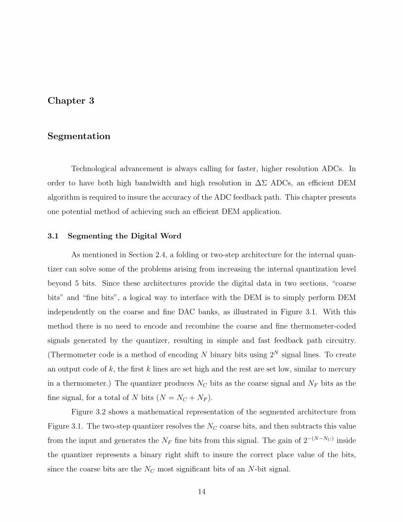
bits” and “fine bits”, a logical way to interface with the DEM is to simply perform DEM
independently on the coarse and fine DAC banks, as illustrated in Figure 3.1. With this
method there is no need to encode and recombine the coarse and fine thermometer-coded
signals generated by the quantizer, resulting in simple and fast feedback path circuitry.
(Thermometer code is a method of encoding N binary bits using 2N signal lines. To create
an output code of k, the first k lines are set high and the rest are set low, similar to mercury
in a thermometer.) The quantizer produces NC bits as the coarse signal and NF bits as the
fine signal, for a total of N bits (N = NC + NF ).
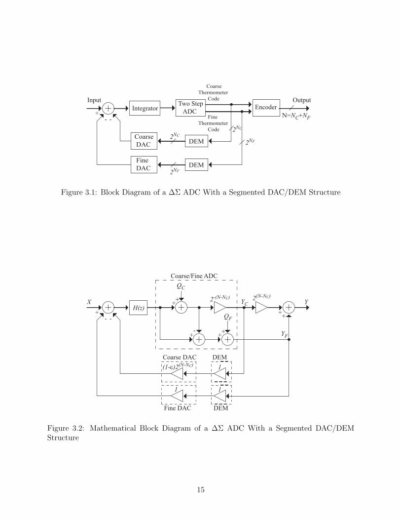
Figure 3.2 shows a mathematical representation of the segmented architecture from
Figure 3.1. The two-step quantizer resolves the NC coarse bits, and then subtracts this value
from the input and generates the NF fine bits from this signal. The gain of 2−(N−NC) inside
the quantizer represents a binary right shift to insure the correct place value of the bits,
since the coarse bits are the NC most significant bits of an N -bit signal.
14
Input
--+
IntegratorOutputTwo Step
ADCEncoder
Coarse DAC
Fine DAC
DEM
DEM
2NC
2NF
CoarseThermometer Code
FineThermometer Code
2NF
2NC
N=NC+NF
Figure 3.1: Block Diagram of a ∆Σ ADC With a Segmented DAC/DEM Structure
X
QC
-+
++
++
Coarse/Fine ADC
DEMCoarse DAC
Fine DAC
(1-ε)2(N-NC)
2-(N-NC)
DEM
--+ QF
H(z)Y
1
1
1
YC
YF
2(N-NC)
++
Figure 3.2: Mathematical Block Diagram of a ∆Σ ADC With a Segmented DAC/DEMStructure
15

0 0.2 0.4 0.6 0.8 182
84
86
88
90
92
94
96
98
100
102SNR vs Element Mismatch
SN
R (
dB)
% Fine Element Mismatch (Coarse is ~1/4 this value)
ReferenceUncalibrated
Figure 3.3: Simulation Results For a Second-Order ∆Σ ADC With a Segmented FeedbackPath
The coarse and fine outputs are each applied to separate DACs using smaller, inde-
pendent DEM circuits, significantly reducing DEM complexity. Since DEM does not change
the digital signal, but only operates on the error within each DAC, the DEM blocks can be
represented as a simple gain of unity, as seen in Figure 3.2. The coarse DAC transfer func-
tion is weighted 2N−NC times that of the fine DAC to represent the place value of the coarse
bits relative to the fine. In practice, this is done by making the elements of the coarse DAC
2N−NC times larger than those of the fine DAC. The quantization noise, QC , present in both
signals YC and YF , ideally will cancel when the coarse and fine signals are summed together
at the modulator input. This result should be the same as if a single DEM circuit with a
single DAC had been in the feedback path. With perfect DACs (0% mismatch), MATLAB
behavioral simulations indicate that this system operates well, as shown in Figure 3.3. But,
as shown in the same Figure, with the addition of unit-element mismatch, the overall SNR
of the system drops much faster than the full 256-element reference case.
16

Unless otherwise noted, all simulations performed for comparison in this thesis use a
second-order ∆Σ ADC architecture with an OSR of 20 and 8 bits of internal quantization.
The reference case is a non-segmented (single-path) architecture, and the others use some
variation of the segmented architecture, splitting the feedback signal into 4 bits for each
of the coarse and fine paths. The percent mismatch of the coarse unit elements is scaled
assuming they are 2N−NC times larger than the fine unit elements, which is typically the
case in a practical application. Random element sizes are generated using the MATLAB
“rand” function. To account for the randomness of the element mismatch, the average of 21
different simulations is taken, with new element values generated for each run.
3.2 Analysis of the Problem
The previous explanation of the system’s operation neglected an important point.
The weighting of the coarse DAC as compared to the fine DAC depends on the relative sizes
of the unit elements. Since the unit elements vary in actual size, the weight of the coarse
DAC will not be exactly 2N−NC , but will be off by the factor 1− ε, as shown in Figure 3.2.
Because of this gain mismatch between the coarse and fine DAC banks, the quantization
noise, QC , will not completely cancel when the coarse and fine signals are summed together,
as they would in the ideal case. The non-canceled portion of the quantization noise will be
added directly to the input signal, and thus be transmitted to the output of the ADC.
The output, Y , of the ADC in Figure 3.2 can be derived as follows:
YC(z) =2−(N−NC)
[QC(z) + (X(z)− YF (z)) H(z)
]1 + (1− ε)H(z)
(3.1)
YF (z) =(−QC(z) + QF (z))
[1 + (1− ε)H(z)
]1 + (1− ε)H(z)
(3.2)
Y (z) = YC(z) · 2N−NC + YF (z) (3.3)
=X(z) ·H(z)
1 + (1− ε)H(z)︸ ︷︷ ︸Desired Signal
+QF (z)
1 + (1− ε)H(z)︸ ︷︷ ︸Expected Noise
+ε · (QC(z)−QF (z))H(z)
1 + (1− ε)H(z)︸ ︷︷ ︸Extra Noise Term
. (3.4)
17
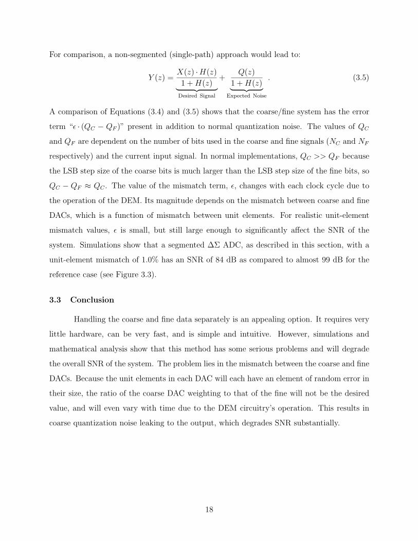
For comparison, a non-segmented (single-path) approach would lead to:
Y (z) =X(z) ·H(z)
1 + H(z)︸ ︷︷ ︸Desired Signal
+Q(z)
1 + H(z)︸ ︷︷ ︸Expected Noise
. (3.5)
A comparison of Equations (3.4) and (3.5) shows that the coarse/fine system has the error
term “ε · (QC − QF )” present in addition to normal quantization noise. The values of QC
and QF are dependent on the number of bits used in the coarse and fine signals (NC and NF
respectively) and the current input signal. In normal implementations, QC >> QF because
the LSB step size of the coarse bits is much larger than the LSB step size of the fine bits, so
QC − QF ≈ QC . The value of the mismatch term, ε, changes with each clock cycle due to
the operation of the DEM. Its magnitude depends on the mismatch between coarse and fine
DACs, which is a function of mismatch between unit elements. For realistic unit-element
mismatch values, ε is small, but still large enough to significantly affect the SNR of the
system. Simulations show that a segmented ∆Σ ADC, as described in this section, with a
unit-element mismatch of 1.0% has an SNR of 84 dB as compared to almost 99 dB for the
reference case (see Figure 3.3).
3.3 Conclusion
Handling the coarse and fine data separately is an appealing option. It requires very
little hardware, can be very fast, and is simple and intuitive. However, simulations and
mathematical analysis show that this method has some serious problems and will degrade
the overall SNR of the system. The problem lies in the mismatch between the coarse and fine
DACs. Because the unit elements in each DAC will each have an element of random error in
their size, the ratio of the coarse DAC weighting to that of the fine will not be the desired
value, and will even vary with time due to the DEM circuitry’s operation. This results in
coarse quantization noise leaking to the output, which degrades SNR substantially.
18

Chapter 4
Calibration
Using a segmented feedback DAC with separate DEM is a potential method to sim-
plify the DEM block and allow it to operate on highly-quantized signals. However, error is
introduced by another mismatch problem, namely, the mismatch between the coarse and fine
DAC banks. As the title suggests, this chapter presents a method to remove that mismatch
using calibration.
4.1 The Motivation For Calibration
The mismatch term, ε, from Equation (3.4) represents the deviation from the desired
gain ratio of the coarse and fine DACs. As mentioned in the previous section, each DAC’s
gain changes with every cycle due to the DEM operation. However, since ∆Σ ADCs use
oversampling, the average gain of the DAC over time is more important than any instanta-
neous value. For an N -bit, fully-differential DAC with M = 2N − 1 unit elements, each of
value Di, the output corresponding to an input code of “n” in the range [0, N ] is equal to:
FD(n) =n∑
i=1
Di −M∑
i=n+1
Di. (4.1)
In words: the output is equal to the sum of the first n elements minus the sum of the
remaining elements. The difference between two successive input codes is then given by:
FD(k)− FD(k − 1) = 2 ·Dk. (4.2)
Since the DAC gain is equal to the average slope of the transfer function, the average gain
of the DAC (A) can be written as:
A =FD(k)− FD(k − 1)
2Dref
=Di
Dref
, (4.3)
19

Table 4.1: Simulated SNR Results for Segmented ∆Σ ADC (in dB)
Unit-Element % Mismatch
0.0 0.5 1.0
Reference 100.8 99.6 98.4Segmented 100.8 89.5 83.8
Segmented withAdjusted DAC Gain
100.8 99.5 98.0
where 2Dref represents the ideal output step size (corresponding to an input LSB change)
and Di is the average unit-element value.
Equation (4.3) states that the average gain of the coarse or fine DAC is equal to the
normalized average element size. So the mismatch, ε, from Equation (3.4) can be reduced
by matching the average element values between DACs with the ratio of 2N−NC : 1. The
individual DAC element values are not important, as long as the average element values
meet this ratio. The (1− ε) factor will be zero on average and the coarse quantization noise
will not leak to the output. Simulated results shown in Table 4.1 demonstrate this. The
first row is the SNR of the reference ∆Σ ADC at various unit-element mismatch values.
The second row shows the standard segmented case. The third row is the same segmented
case, with a single fine unit element adjusted such that the average unit-element value in
the coarse DAC is exactly 16 times larger than the average unit-element value in the fine
DAC (28−4 : 1 = 16 : 1). At 1% mismatch, the segmented ADC without equalized DAC
gains has an SNR 14.6 dB lower than the reference (non-segmented) case. In comparison,
the ADC with adjusted DAC gains has an SNR only 0.4 dB lower than the reference case.
Such adjustment of the DAC gains can be acheived through calibration.
4.2 The Calibration Method
Figure 4.1 is a block diagram of a proposed calibration architecture. This method
performs the calibration as an initialization step. During calibration, the connections from
the coarse/fine ADC to the feedback path are broken and a single-bit path provides the
20

InputAdditional Stages
DEM
Coarse DAC
DEM
- -
+Output Coarse/
Fine ADC
One-Bit ADC
Synck Filter andCalibration Logic
1-bit Cal DAC
-
CAL
Test Signal
CAL
CAL
Cal
ibra
tion
Si
gnal
CAL
CAL
CAL
FineDAC
CAL
1
CAL
0
Figure 4.1: Block Diagram of Calibration Method
modulator feedback. A one-bit quantizer is used because it is immune to the mismatch that
plagues multi-bit quantizers. The modulator input is grounded and a fixed, DC test signal
is presented to the coarse and fine DACs through the DEM circuitry. The output is sent
to an averaging synck filter, and then measured for each DAC individually, with the other
DACs disconnected from the circuit. The relative measurement between coarse and fine
DAC banks can then be used to make the necessary adjustment to match the ratio of the
average DAC element values. Simulations show that the calibration routine must measure
coarse and fine average capacitor values to within 2.5% of their nominal values to keep SNR
penalties below 2 dB. This means that the one-bit modulator must measure the calibration
signal to within 0.0098% of full scale (13 to 14-bit accuracy); this is feasible for a one-bit
modulator with high oversampling.
Correction must be applied to one of the DACs to complete the calibration. Due
to the averaging effect of the DEM algorithm, the required adjustment does not have to
be added to all the unit elements in the bank. Simulations show that it is sufficient to
manipulate a single fine unit element to achieve the required average unit-element ratio.
21

Similarly adjusting a coarse bank element is not effective; two possible explanations for this
are as follows: 1) the mismatch between individual coarse bank elements may be increased,
reducing the effectiveness of coarse-bank DEM, and 2) the coarse DAC input data is more
strongly patterned than the fine DAC input data, therefore DEM averaging is performed
less efficiently in the coarse DAC.
4.3 Drawbacks and Benefits
A distinct advantage of the calibration method is the low complexity of the feedback
path. For an 8-bit quantizer, two independent, 4-bit DEM implementations are required.
These DEM algorithms can be constructed so that only a four-stage pass-gate structure is
required in the signal path to shuffle the thermometer-coded ADC outputs [13]. Thus both
the complexity and the timing delay of the digital feedback path are minimal.
The necessity of having a separate calibration mode is a significant drawback. The
device is not ready for immediate use, and cannot track changes in circuit behavior relating
to temperature and other time-varying effects. A possible solution is to use a background
calibration routine, such as one that uses an out-of-band DAC test sequence as proposed
in [14]. Another drawback is that the calibration circuitry can be quite complex and large,
requiring a lot of control circuitry and memory to compute and apply the required calibration
adjustment. Also, as separate DACs are generally used for each integration stage in ∆Σ
modulators, each set of DAC banks must be calibrated individually, which adds to the time
required to calibrate high-order modulators. Exactly how to apply the calibration adjustment
in such a way that does not add additional error is also a non-trivial problem.
4.4 Behavioral Simulation Results
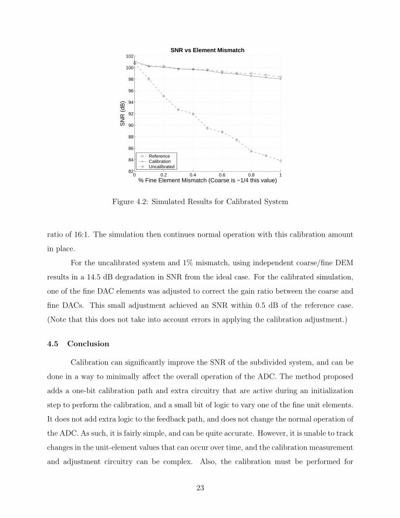
Figure 4.2 shows simulation results for both calibrated and uncalibrated systems com-
pared to the reference case for various unit-element mismatch percentages. In the calibration
simulation, a “calibration mode” is simulated using a 1-bit ADC and feedback path, and
alternately applying a test signal to the coarse and fine DAC to measure their individual
effects on the output. These individual measurements are then compared and used to cal-
culate how much a single fine element must be adjusted to insure an average element size
22
0 0.2 0.4 0.6 0.8 182
84
86
88
90
92
94
96
98
100
102SNR vs Element Mismatch
SN
R (
dB)
% Fine Element Mismatch (Coarse is ~1/4 this value)
ReferenceCalibrationUncalibrated
Figure 4.2: Simulated Results for Calibrated System
ratio of 16:1. The simulation then continues normal operation with this calibration amount
in place.
For the uncalibrated system and 1% mismatch, using independent coarse/fine DEM
results in a 14.5 dB degradation in SNR from the ideal case. For the calibrated simulation,
one of the fine DAC elements was adjusted to correct the gain ratio between the coarse and
fine DACs. This small adjustment achieved an SNR within 0.5 dB of the reference case.
(Note that this does not take into account errors in applying the calibration adjustment.)
4.5 Conclusion
Calibration can significantly improve the SNR of the subdivided system, and can be
done in a way to minimally affect the overall operation of the ADC. The method proposed
adds a one-bit calibration path and extra circuitry that are active during an initialization
step to perform the calibration, and a small bit of logic to vary one of the fine unit elements.
It does not add extra logic to the feedback path, and does not change the normal operation of
the ADC. As such, it is fairly simple, and can be quite accurate. However, it is unable to track
changes in the unit-element values that can occur over time, and the calibration measurement
and adjustment circuitry can be complex. Also, the calibration must be performed for
23

each group of DAC banks, meaning that increasing the order of the ∆Σ modulator will
significantly increase the time required to fully calibrate the ADC.
24

Chapter 5
Requantization
The previous chapter showed that calibration is a viable option for eliminating the
error added by the segmented DEM approach. However, the operation of the DEM blocks
themselves suggests another solution. The DEM blocks function not by removing the error
in the DAC elements, but by shifting the noise caused by that error away from the band of
interest. This chapter presents a noise-shaping method that attempts to do the same with
the noise caused by the coarse and fine DAC bank mismatch.
5.1 The Noise-Shaped Requantization (ReQ) Method
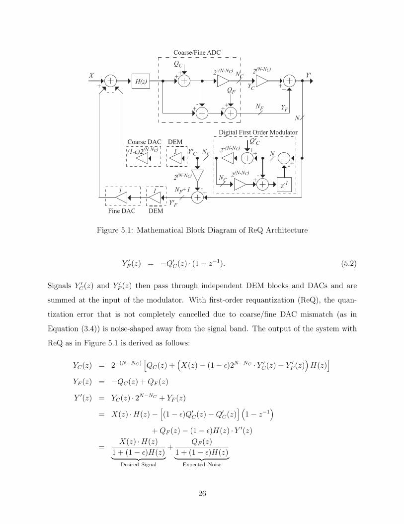
This method was initially proposed in [6] for a ∆Σ DAC; this work extends this
concept to ∆Σ ADCs. The basic idea is to generate a new coarse signal with a digital ∆Σ
modulator and use this coarse signal to generate a new fine signal. This insures that both
the coarse and fine signals are individually noise shaped, which is performed in a way that
causes the quantization error leakage to be noise shaped as well. Even though it does not
completely cancel errors due to DAC mismatch, the quantization error noise power will be
outside the signal band. The process is explained below, and is modeled in Figure 5.1.
First, the coarse and fine signals from the ADC internal quantizer are encoded into
binary and concatenated to form a 2’s complement N -bit signal, Y ′. This signal is then
requantized to NC bits to form a new coarse signal using a digital first-order ∆Σ modulator.
This coarse signal is subtracted from the original N -bit signal to form the new fine signal,
comprised of NF +1 bits. After requantization, the new coarse and fine signals are:
Y ′C(z) = 2−(N−NC)
[Y ′(z) + Q′
C(z)(1− z−1
)](5.1)
25
X
QC
-+
++
++
Coarse/Fine ADC
DEMCoarse DAC
Fine DAC
(1-ε)2(N-NC)
2-(N-NC)
DEM
--+ QF
H(z)Y'
1
1
1
YC
YF
2(N-NC)
++
+-
Q'C++
Z-1+-
Digital First Order Modulator
N
N
+-
2(N-NC)
NC
NF+1
NC
NF
NC
Y'C
Y'F
2(N-NC)
2-(N-NC)
Figure 5.1: Mathematical Block Diagram of ReQ Architecture
Y ′F (z) = −Q′
C(z) · (1− z−1). (5.2)
Signals Y ′C(z) and Y ′
F (z) then pass through independent DEM blocks and DACs and are
summed at the input of the modulator. With first-order requantization (ReQ), the quan-
tization error that is not completely cancelled due to coarse/fine DAC mismatch (as in
Equation (3.4)) is noise-shaped away from the signal band. The output of the system with
ReQ as in Figure 5.1 is derived as follows:
YC(z) = 2−(N−NC)[QC(z) +
(X(z)− (1− ε)2N−NC ·Y ′
C(z)− Y ′F (z)
)H(z)
]YF (z) = −QC(z) + QF (z)
Y ′(z) = YC(z) · 2N−NC + YF (z)
= X(z) ·H(z)−[(1− ε)Q′
C(z)−Q′C(z)
] (1− z−1
)+ QF (z)− (1− ε)H(z) ·Y ′(z)
=X(z) ·H(z)
1 + (1− ε)H(z)︸ ︷︷ ︸Desired Signal
+QF (z)
1 + (1− ε)H(z)︸ ︷︷ ︸Expected Noise
26
100
102
104
−150
−100
−50
0
50
100
Frequency
Pow
er
100
102
104
−150
−100
−50
0
50
100
Frequency
Power Spectra
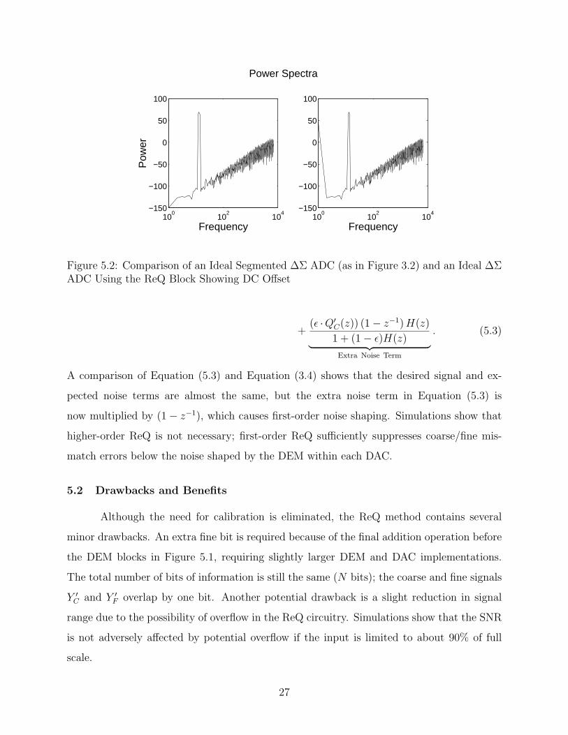
Figure 5.2: Comparison of an Ideal Segmented ∆Σ ADC (as in Figure 3.2) and an Ideal ∆ΣADC Using the ReQ Block Showing DC Offset
+(ε ·Q′
C(z)) (1− z−1) H(z)
1 + (1− ε)H(z)︸ ︷︷ ︸Extra Noise Term
. (5.3)
A comparison of Equation (5.3) and Equation (3.4) shows that the desired signal and ex-
pected noise terms are almost the same, but the extra noise term in Equation (5.3) is
now multiplied by (1− z−1), which causes first-order noise shaping. Simulations show that
higher-order ReQ is not necessary; first-order ReQ sufficiently suppresses coarse/fine mis-
match errors below the noise shaped by the DEM within each DAC.
5.2 Drawbacks and Benefits
Although the need for calibration is eliminated, the ReQ method contains several
minor drawbacks. An extra fine bit is required because of the final addition operation before
the DEM blocks in Figure 5.1, requiring slightly larger DEM and DAC implementations.
The total number of bits of information is still the same (N bits); the coarse and fine signals
Y ′C and Y ′
F overlap by one bit. Another potential drawback is a slight reduction in signal
range due to the possibility of overflow in the ReQ circuitry. Simulations show that the SNR
is not adversely affected by potential overflow if the input is limited to about 90% of full
scale.
27
A third drawback comes in the form of a DC error that occurs when using the ReQ
method. Even when simulations are performed using ideal unit elements, some DC offset is
present. Figure 5.2 demonstrates this. The left half of the picture shows the power spectrum
for a segmented ∆Σ ADC with ideal elements. The right half shows the same signal, this
time from a ∆Σ ADC with ReQ operating in the feedback path. The ReQ signal shows
first-order noise shaping of the quantization noise leakage, but it also has a DC component.
This DC offset arises due to the difference between YF and Y ′F . The signal YF is an unsigned
number (the lower bits of a 2’s complement number), while Y ′F is a 2’s complement number,
which can be either positive or negative. An analysis of the source of this DC error follows.
In a system using unsigned numbers (positive integers), a fully-differential DAC can
be modeled by the following equation:
D(Y ) =Vref
2N − 1
(Y)− Vref
2N − 1
[(2N − 1
)−(Y)]
. (5.4)
(A fully-differential DAC is one that always uses all of the elements, each in either the
“positive” or the “negative” sense.) In a 2’s complement DAC, the equation for D(Y ) is
slightly different:
D(Y ) =Vref
2N − 1
(Y + 2N−1
)− Vref
2N − 1
[(2N − 1
)−(Y + 2N−1
)]. (5.5)
The first term represents the elements that are “on,” or added, and the second term rep-
resents the elements that are “off,” or subtracted. In these equations, Vref is the reference
voltage for the DAC, and 2N − 1 is representative of how many individual levels the DAC
can represent. The term Y + 2N−1 in Equation (5.5) results from the need to convert the
2’s complement number “Y ” to a positive number representing how many unit elements to
use in the “positive” sense (the rest are “negative”, as shown by the second term in the
equation). Through some simplification it is easy to show that the 2’s complement DAC
equation reduces to:
D(Y ) =Vref
2N − 1(2 ·Y + 1) . (5.6)
28
For a basic coarse/fine system with no ReQ step inserted, as in Figure 3.2, since YC is
a 2’s complement number, and YF is an unsigned number, the following equations describe
the output of the DACs:
DC(YC) =Vref · 2N−NC
2N − 1
(YC + 2NC−1
)− Vref · 2N−NC
2N − 1
[(2NC − 1
)−(YC + 2NC−1
)](5.7)
DF (YF ) =Vref
2N − 1(YF )− Vref
2N − 1
[(2NF − 1
)− (YF )
]. (5.8)
The sum of the output of these two DACs with the input of YC and YF should be the same
as the output of a single DAC with the input of Y (see Equation (5.6)):
DC(YC) + DF (YF ) =Vref
2N − 1
[2 · 2N−NC
(YC + 2NC−1
)+ 2 (YF )
−2N−NC
(2NC − 1
)−(2NF − 1
)]=
Vref
2N − 1
[2(2N−NC ·YC + YF + 2N−NC · 2NC−1
)−(2N − 1
)−(−2N−NC + 2NF
)]=
Vref
2N − 1
[2(Y + 2N−1
)−(2N − 1
)]=
Vref
2N − 1(2 ·Y + 1) . (5.9)
This shows that the two separate DACs together perform exactly the same function that a
single DAC (as in the reference design) would do: D(Y ) = DC(YC) + DF (YF ).
When this same analysis is applied to the ReQ system (as in Figure 5.1), a slightly
different result is obtained. Both Y ′C and Y ′
F are 2’s complement numbers, and Y ′F has one
more bit than YF . So the DAC equations are:
D′C(Y ′
C) =Vref · 2N−NC
2N − 1
(Y ′
C + 2NC−1)
− Vref · 2N−NC
2N − 1
[(2NC − 1
)−(Y ′
C + 2NC−1)]
(5.10)
D′F (Y ′
F ) =Vref
2N − 1
(Y ′
F + 2NF
)− Vref
2N − 1
[(2NF +1 − 1
)−(Y ′
F + 2NF
)]. (5.11)
29
The sum of D′C(Y ′
C) and D′F (Y ′
F ) should be the same as a single DAC with an input of Y ′.
However, it is not. The sum is instead given by:
D′C(Y ′
C) + D′F (Y ′
F ) =Vref
2N − 1
[2 · 2N−NC
(Y ′
C + 2NC−1)
+ 2(Y ′
F + 2NF
)−2N−NC
(2NC − 1
)−(2NF +1 − 1
)]=
Vref
2N − 1
[2(2N−NC ·Y ′
C + Y ′F + 2N−NC · 2NC−1
)−(2N − 1
)+(2 · 2NF + 2N−NC − 2NF +1
)]=
Vref
2N − 1
[2(2N−NC ·Y ′
C + Y ′F + 2N−1
)−(2N − 1
)+(2NF +1 − 2NF
)]=
Vref
2N − 1
[2(Y + 2N−1
)−(2N − 1
)+(2NF
)]=
Vref
2N − 1(2 ·Y + 1)︸ ︷︷ ︸
Desired Signal
+Vref
2N − 1
(2NF
)︸ ︷︷ ︸
Offset
. (5.12)
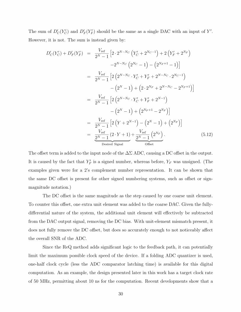
The offset term is added to the input node of the ∆Σ ADC, causing a DC offset in the output.
It is caused by the fact that Y ′F is a signed number, whereas before, YF was unsigned. (The
examples given were for a 2’s complement number representation. It can be shown that
the same DC offset is present for other signed numbering systems, such as offset or sign-
magnitude notation.)
The DC offset is the same magnitude as the step caused by one coarse unit element.
To counter this offset, one extra unit element was added to the coarse DAC. Given the fully-
differential nature of the system, the additional unit element will effectively be subtracted
from the DAC output signal, removing the DC bias. With unit-element mismatch present, it
does not fully remove the DC offset, but does so accurately enough to not noticeably affect
the overall SNR of the ADC.
Since the ReQ method adds significant logic to the feedback path, it can potentially
limit the maximum possible clock speed of the device. If a folding ADC quantizer is used,
one-half clock cycle (less the ADC comparator latching time) is available for this digital
computation. As an example, the design presented later in this work has a target clock rate
of 50 MHz, permitting about 10 ns for the computation. Recent developments show that a
30

two-step ADC architecture can be used while still allowing this same amount of propagation
time for the logic [10, 11]. With careful design, the delay through this path should be small
enough, and as CMOS technology scales, the delay will continue to decrease, permitting
faster clock rates.
The benefits to offset these drawbacks are few, but significant. First, there is no
startup mode required, providing “instant-on” functionality. Second, since this method of
removing the DAC mismatch error is completely digital, the actual chip should operate very
close to the simulation. In the case of calibration, there are additional inaccuracies that
will be present in physical silicon (such as the circuits to apply the calibration change and a
limited number of bits to represent the measurements) that were not taken into account in
the simulations. So the ReQ method is potentially easier to implement and easier to achieve
functionality in silicon.
5.3 Behavioral Circuit Simulation Results
Figure 5.3 compares the performance of the calibration and ReQ methods against the
ideal (full DEM) case. For the case of 1% fine element mismatch, the ReQ method achieves
an average SNR of 96.5 dB, which is only 2 dB less than the full 8-bit DEM reference case.
The calibration method acheives slighty superior performance in simulation, but would be
much harder to effectively implement in silicon.
5.4 Conclusion
The ReQ method applies techniques developed for ∆Σ DACs to the ADC feedback
path. The coarse and fine signals are reassigned using a first-order digital modulator, and
then applied to the DEM and DAC circuits. The resulting system has slightly worse SNR
performance than the calibration method previously discussed, but it does not require any
special initialization or setup in order to work, and is potentially easier to implement.
This method adds significant delay to the feedback path, and adds some area and
power consumption for the required circuitry. However, operation very near the reference
case is achieved, and no additional steps or circuitry are required to use this method with
higher-order ∆Σ modulators.
31
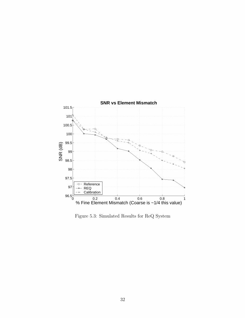
0 0.2 0.4 0.6 0.8 196.5
97
97.5
98
98.5
99
99.5
100
100.5
101
101.5SNR vs Element Mismatch
SN
R (
dB)
% Fine Element Mismatch (Coarse is ~1/4 this value)
ReferenceREQCalibration
Figure 5.3: Simulated Results for ReQ System
32

Chapter 6
Circuit Design
Both the calibration and requantization methods previously discussed are successful
and efficient methods to implement a segmented DEM architecture. The physical realization
of the calibration method depends on analog circuits to apply the calibration. The ReQ
method, however, is completely digital in its implementation. As such, the physical operation
of the ReQ method should be closer to its simulated performance than that of the calibration
method. For this reason, the ReQ method was chosen as the solution for the current research
application. This chapter presents the circuit designs to implement the ReQ method in
silicon.
6.1 Circuit Overviews
The ReQ circuits presented in this chapter are designed to meet the following system
specifications in a TSMC 0.25 µm process: fourth-order ∆Σ ADC, 50 MHz clock rate,
NC = 4, and NF = 4. Straight-forward designs were used (circuits without many speed
optimizations) to see if standard circuits could be used to meet the time delay constraints.
Due to the lack of available synthesis tools, the designs were done by hand, instead of using
RTC. The overall block diagram of the feedback path is shown in Figure 6.1. Each block
will be explained in turn, and full schematics for each can be found in Appendix A.
6.1.1 Encoder
The first blocks in the feedback path are the two encoders. These identical blocks
first convert the thermometer code output of the ADC quantizer into a “one-hot” signal (a
signal in which only one wire is asserted at any given time). In order to do this, the circuitry
33

DEM
Coarse DAC
FineDAC
DEM
--
ReQBlock
Encoders
Decoders
2NF2NC
2NF+1
NFNCNC
NF+12NF+1
2NC
2NC
InputAdditional Stages
+
Output Coarse/Fine ADC
Figure 6.1: Overall Block Diagram of the Feedback Path for the ReQ Method
looks for the edge of the thermometer code - a sequence of “0 0 1”. A three-input detection
allows the circuit to eliminate a spurious code of “1 0 1” (referred to as a “bubble”). The
circuit is comprised of 3-input nor gates and inverters. Figure 6.2 shows this part of the
design.
After this, the encoders convert the “one-hot” signals to binary. Since the output
of these two blocks represent, respectively, the four most significant bits and four least
significant bits of the 2’s complement binary number, the circuits are slightly different: the
encoder block for the most significant bits has an extra inverter on the MSB to make it
output 2’s complement signed numbers. Figure 6.3 shows the circuit design for the encoder
handling the most significant bits, and Figure 6.4 shows the circuit design for the encoder
handling the least significant bits. The circuits were designed using weak p-type pull-up
devices to hold the outputs high, unless pulled low by strong n-type devices controlled by
the input signals.
6.1.2 ReQ Block
The ReQ circuit (see Figure 6.5) is comprised of two 8-bit subtractors, a 5-bit sub-
tractor, and an 8-bit register. The lower right part of Figure 5.1 shows a block diagram view
34

I34
I31
I32
I29
I28
I33
I27
I26
I25
I24
I23
I22
I21
I20
I19
I18
I17
I16
I15
I14
I13
I12
I11
I9
I8
I7
I6
I5
I4
I3
I2
I1
I0
gnd
vdd
gnd
vdd
gnd
vdd
gnd
vdd
gnd
vdd
gnd
vdd
gnd
vdd
gnd
vdd
gnd
vdd
gnd
vdd
gnd
vdd
gnd
vdd
gnd
vdd
gnd
vdd
gnd
vdd
gnd
vdd
gnd
vdd
gnd
vdd
gnd
vdd
Q
A
B
C
gnd
vdd
Q
A
B
C
gnd
vdd
Q
A
B
C
gnd
vdd
Q
A
B
C
gnd
vdd
Q
A
B
C
gnd
vdd
Q
A
B
C
gnd
vdd
Q
A
B
C
gnd
vdd
Q
A
B
C
gnd
vdd
Q
A
B
C
gnd
vdd
Q
A
B
C
gnd
vdd
Q
A
B
C
gnd
vdd
Q
A
B
C
gnd
vdd
Q
A
B
C
gnd
vdd
Q
A
B
C
gnd
vdd
Q
A
B
C
vdd
gnd
TC<15:1>
one_high<15:1>
TC<15> in
vdd
gnd
inverter_1b
out
TC<14> in
vdd
gnd
inverter_1b
out
TC<13> in
vdd
gnd
inverter_1b
out
TC<14> in
vdd
gnd
inverter_1b
out
TC<13> in
vdd
gnd
inverter_1b
out
TC<15>
TC<15>
TC<14>
TC<13> in
vdd
gnd
inverter_1b
out
TC<14>
TC<13>
TC<12> in
vdd
gnd
inverter_1b
out
TC<13>
TC<12>
TC<11> in
vdd
gnd
inverter_1b
out
TC<12>
TC<11>
TC<10> in
vdd
gnd
inverter_1b
out
TC<11>
TC<10>
TC<9> in
vdd
gnd
inverter_1b
out
one_high<15>NOR3
vdd
gnd
one_high<14>NOR3
vdd
gnd
one_high<13>NOR3
vdd
gnd
one_high<12>NOR3
vdd
gnd
one_high<11>NOR3
vdd
gnd
one_high<10>NOR3
vdd
gnd
one_high<9>NOR3
vdd
gnd
TC<3>
TC<2>
TC<1> in
vdd
gnd
inverter_1b
out
one_high<1>NOR3
vdd
gnd
TC<4>
TC<3>
TC<2> in
vdd
gnd
inverter_1b
out
one_high<2>NOR3
vdd
gnd
TC<5>
TC<4>
TC<3> in
vdd
gnd
inverter_1b
out
one_high<3>NOR3
vdd
gnd
TC<6>
TC<5>
TC<4> in
vdd
gnd
inverter_1b
out
one_high<4>NOR3
vdd
gnd
TC<7>
TC<6>
TC<5> in
vdd
gnd
inverter_1b
out
one_high<5>NOR3
vdd
gnd
TC<8>
TC<7>
TC<6> in
vdd
gnd
inverter_1b
out
one_high<6>NOR3
vdd
gnd
TC<9>
TC<8>
TC<7> in
vdd
gnd
inverter_1b
out
one_high<7>NOR3
vdd
gnd
TC<10>
TC<9>
TC<8> in
vdd
gnd
inverter_1b
out
one_high<8>NOR3
vdd
gnd
Figure 6.2: Bubble Decode Circuitry
35

l :240.0n
w=1.16u
"nch"
fingers:1
m:1
l:240.0n
w=1.16u
"nch"
fingers:1
m:1
l:240.0n
w=1.16u
"nch"
fingers:1
m:1
l:240.0n
w=1.16u
"nch"
fingers:1
m:1
l:240.0n
w=580.0n
"nch"
fingers:1
m:1
l:240.0n
w=580.0n
"nch"
fi ngers:1
m:1
l:240.0n
w=580.0n
"nch"
fingers:1
m:1
l:240.0n
w=580.0n
"nch"
fingers:1
m:1
l:240.0n
w=580.0n
"nch"
fingers:1
m:1
l:240.0n
w=580.0n
"nch"
fingers:1
m:1
l :240.0n
w=580.0n
"nch"
fingers:1
m:1
l:240.0n
w=580.0n
"nch"
fingers:1
m:1
l:240.0n
w=580.0n
"nch"
fingers:1
m:1
l:240.0n
w=580.0n
"nch"
fingers:1
m:1
l:240.0n
w=580.0n
"nch"
fingers:1
m:1
l:240.0n
w=580.0n
"nch"
fingers:1
m:1
l:240.0n
w=580.0n
"nch"
fingers:1
m:1
l:240.0n
w=580.0n
"nch"
fingers:1
m:1
l:240.0n
w=580.0n
"nch"
fingers:1
m:1
l:240.0n
w=580.0n
"nch"
fingers:1
m:1
l:240.0n
w=580.0n
"nch"
fingers:1
m:1
l:240.0n
w=580.0n
"nch"
fingers:1
m:1
l:240.0n
w=580.0n
"nch"
fingers:1
m:1
l:240.0n
w=580.0n
"nch"
fingers:1
m:1
l:240.0n
w=580.0n
"nch"
fingers:1
m:1
l:240.0n
w=580.0n
"nch"
fingers:1
m:1
l:240.0n
w=580.0n
"nch"
fingers:1
m:1
l:240.0n
w=580.0n
"nch"
fingers:1
m:1
l:240.0n
w=580.0n
"nch"
fingers:1
m:1
l:240.0n
w=580.0n
"nch"
fingers:1
m:1
l:240.0n
w=580.0n
"nch"
fingers:1
m:1
l:240.0n
w=580.0n
"nch"
fingers:1
m:1
l:240.0n
w=580.0n
"nch"
fingers:1
m:1
l:240.0n
w=580.0n
"nch"
fingers:1
m:1
l:240.0n
w=580.0n
"nch"
fingers:1
m:1
l:240.0n
w=580.0n
"nch"
fingers:1
m:1
l:240.0n
w=1.16u
"nch"
fingers:1
m:1
m:1
"pch"
w=1.74u
l:240.0n
fingers=3
m:1
"pch"
w=1.74u
l: 240.0n
fingers=3
m:1
"pch"
w=1.74u
l:240.0n
fingers=3
m:1
"pch"
w=1.74u
l:240.0n
fingers=3
m:1
"pch"
w=580.0n
l:240.0n
fingers:1
m:1
"pch"
w=580.0n
l:240.0n
fingers:1
m:1
"pch"
w=1.74u
l:240.0n
fingers=3
m:1
"pch"
w=580.0n
l:240.0n
fingers:1
m:1
"pch"
w=580.0n
l:240.0n
fingers:1
NM30
NM97
NM31
NM32
NM33NM34NM35NM36
NM37 NM38 NM39
NM43NM44
NM45 NM46 NM48
NM49NM52
NM53
NM58NM60
NM61 NM63 NM64
NM72
NM75
NM77NM78
NM82
NM85NM87
NM90NM91
NM94 NM95 NM96
NM1
PM34
PM37
PM35
PM36
PM32PM30
PM1
PM31 PM33
vdd
bit<2>
vdd
gnd
gnd
vdd
bit<0>
bit<1>
vdd
gnd
one_high<15>
one_high<2>
vdd
gnd
one_high<1>
one_high<5>
one_high<6>
one_high<4>
one_high<3>
one_high<11>
one_high<12>
one_high<13>
one_high<14>
one_high<9>
one_high<10>
one_high<8>
one_high<7>
bit<3>
vdd
gnd
gnd
one_high<15:1>
bit<3:0>
gndvdd
Both N and P type devices in array are w/l=540n/240n.
Inverters are P:w/l=1.74u/240n N:w/l=1.16u/240n.
Figure 6.3: Encoder Circuit for the MSBs
36

l :240.0n
w=1.16u
"nch"
fingers:1
m:1
l:240.0n
w=1.16u
"nch"
fingers:1
m:1
l:240.0n
w=1.16u
"nch"
fingers:1
m:1
l:240.0n
w=580.0n
"nch"
fingers:1
m:1
l:240.0n
w=580.0n
"nch"
fi ngers:1
m:1
l:240.0n
w=580.0n
"nch"
fingers:1
m:1
l:240.0n
w=580.0n
"nch"
fingers:1
m:1
l:240.0n
w=580.0n
"nch"
fingers:1
m:1
l:240.0n
w=580.0n
"nch"
fingers:1
m:1
l :240.0n
w=580.0n
"nch"
fingers:1
m:1
l:240.0n
w=580.0n
"nch"
fingers:1
m:1
l:240.0n
w=580.0n
"nch"
fingers:1
m:1
l:240.0n
w=580.0n
"nch"
fingers:1
m:1
l:240.0n
w=580.0n
"nch"
fingers:1
m:1
l:240.0n
w=580.0n
"nch"
fingers:1
m:1
l:240.0n
w=580.0n
"nch"
fingers:1
m:1
l:240.0n
w=580.0n
"nch"
fingers:1
m:1
l:240.0n
w=580.0n
"nch"
fingers:1
m:1
l:240.0n
w=580.0n
"nch"
fingers:1
m:1
l:240.0n
w=580.0n
"nch"
fingers:1
m:1
l:240.0n
w=580.0n
"nch"
fingers:1
m:1
l:240.0n
w=580.0n
"nch"
fingers:1
m:1
l:240.0n
w=580.0n
"nch"
fingers:1
m:1
l:240.0n
w=580.0n
"nch"
fingers:1
m:1
l:240.0n
w=580.0n
"nch"
fingers:1
m:1
l:240.0n
w=580.0n
"nch"
fingers:1
m:1
l:240.0n
w=580.0n
"nch"
fingers:1
m:1
l:240.0n
w=580.0n
"nch"
fingers:1
m:1
l:240.0n
w=580.0n
"nch"
fingers:1
m:1
l:240.0n
w=580.0n
"nch"
fingers:1
m:1
l:240.0n
w=580.0n
"nch"
fingers:1
m:1
l:240.0n
w=580.0n
"nch"
fingers:1
m:1
l:240.0n
w=580.0n
"nch"
fingers:1
m:1
l:240.0n
w=580.0n
"nch"
fingers:1
m:1
l:240.0n
w=580.0n
"nch"
fingers:1
m:1
l:240.0n
w=1.16u
"nch"
fingers:1
m:1
m:1
"pch"
w=1.74u
l:240.0n
fingers=3
m:1
"pch"
w=1.74u
l:240.0n
fingers=3
m:1
"pch"
w=1.74u
l:240.0n
fingers=3
m:1
"pch"
w=580.0n
l:240.0n
fingers:1
m:1
"pch"
w=580.0n
l:240.0n
fingers:1
m:1
"pch"
w=1.74u
l:240.0n
fingers=3
m:1
"pch"
w=580.0n
l:240.0n
fingers:1
m:1
"pch"
w=580.0n
l:240.0n
fingers:1
NM30
NM31
NM32
NM33NM34NM35NM36
NM37 NM38 NM39
NM43NM44
NM45 NM46 NM48
NM49NM52
NM53
NM58NM60
NM61 NM63 NM64
NM72
NM75
NM77NM78
NM82
NM85NM87
NM90NM91
NM94 NM95 NM96
NM1
PM34
PM35
PM36
PM32PM30
PM1
PM31 PM33
vdd
bit<2>
vdd
gnd
gnd
vdd
bit<0>
bit<1>
vdd
gnd
one_high<15>
one_high<2>
one_high<1>
one_high<5>
one_high<6>
one_high<4>
one_high<3>
one_high<11>
one_high<12>
one_high<13>
one_high<14>
one_high<9>
one_high<10>
one_high<8>
one_high<7>
vdd
gnd
gnd
one_high<15:1>
bit<3:0>
gndvdd
Both N and P type devices in array are w/l=540n/240n.
Inverters are P:w/l=1.74u/240n N:w/l=1.16u/240n.
bit<3>
Figure 6.4: Encoder Circuit for the LSBs
37
of the ReQ. The path including the register and the two 8-bit subtractors makes up a first-
order digital modulator to form a new noise-shaped coarse signal, and the 5-bit subtractor
is used to form the new noise-shaped fine signal.
The subtractors are a simple ripple-carry design. Since they are only 8 or 5 bits wide,
the potential speedup of carry lookahead circuits is small, and does not seem to offset the
drawback of the increased size and power requirements. The basic full adder circuit is shown
in Figure 6.6.
The D-flip-flops are a standard design, such as can be found in textbooks and web
tutorials. Each flip-flop is made up of two anti-parallel inverters connected in a loop, with
pass gates to break the feedback and connect the input signal when the controlling clock
is high. Register setup and hold times are difficult to simulate without accurate transistor
models, so care was taken to allow a generous amount of time for setup and hold. The circuit
used in this design is shown in Figures 6.7 and 6.8.
6.1.3 Decode Logic
The decode logic is a collection of complex gates to realize the conversion from 4-
or 5-bit binary to thermometer code. The logic was generated by hand using standard
logic tables and k-maps. As an example, Table 6.1 shows the desired operation of the 4-bit
binary-to-thermometer code conversion. The table for the 5-bit binary-to-thermometer code
conversion follows the same pattern.
Since larger devices require more power, the transistors in the complex gates are
all minimum size. This slows down the logic somewhat, but it is still fast enough for this
application. Figures 6.9 and 6.10 show the schematics of the two decoder blocks.
6.1.4 DEM Logic
The DEM logic was designed using the methods presented in [13]. Figure 6.11 shows
the basic operational blocks of the DEM logic for the coarse path: the rotate block and the
rotate control. The rotate control logic takes the binary output signal from the ReQ logic
and adds it to the current value stored in the pointer register. Since the current input code
38
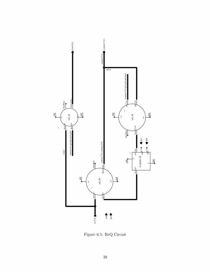
I8
I11
I12
I9
gnd
vdd
<7:0>
GN
D
VD
D
gnd
vdd
GN
D
VD
D
GN
D
VD
D
Sum
<4:0
>
Ove
rflow
A<4
:0>
B<4
:0>
sub_
5b
<4:0
>
coar
se<4
>,gn
d,gn
d,gn
d,gn
d
gnd
vdd
Sum
<7:0
>
Ove
rflow
A<7
:0>
B<7
:0>
sub_
8b
gnd
vdd
in<7
:0>
coar
se<7
:4>,
coar
se<3
:0>
coar
se<7
:4>
coar
se<7
:4>
fine<
4:0>
coar
se<7
:4>,
gnd,
gnd,
gnd,
gnd
gnd
vdd
Sum
<7:0
>
Ove
rflow
A<7
:0>
B<7
:0>
sub_
8b
clk1
clk2
d-re
gist
er_8
b
Q<7
:0>
D<7
:0>
clk1
clk2
gnd
vdd
Figure 6.5: ReQ Circuit
39

Sum Cou
t
A
B Cin
Cin
BA
BAB
CinA
Cin B A
AA
ACin
Cin
B
B
B
VD
D
GN
D
Cou
t
Sum
Cin BA
PM0
PM1
PM2
NM
0
NM
1N
M2
NM
4
NM
3
PM
3
PM
4
PM
5
PM
6
PM
7P
M8
NM
5
NM
6
NM
7N
M8
PM
10
PM
9
PM
11
NM
11
NM
10
NM
9
NM
12
PM
12
PM
13
NM
13
All P-type devices:l=240nw=1.74u
All N-type devices:l=240nw=580n
Figure 6.6: Full Adder Circuit
40
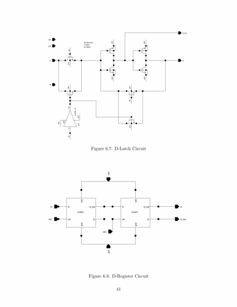
inve
rter_
1b
gnd
gnd
vdd
gnd
vdd
clk
gnd
gnd
vdd
vdd
vdd
D
Q_bar
Q
vdd
gnd
gndvd
d
out
incl
kcl
k
clk
All devices:l=240nw=580n
Figure 6.7: D-Latch Circuit
d-latchd-latch
gnd
vdd
Q_bar
QD
clk2
clk1
gnd
vdd
Q
Q_barD
clk
gnd
vdd
Q
Q_barD
clk
Figure 6.8: D-Register Circuit
41

vdd
vddgnd
b<3:0>
TC_bar<14:0>
vdd
vdd
vdd vdd
vdd
vdd vdd
vdd
vdd
vdd vdd
vdd
vdd
vdd
vdd
vdd
vddvdd
vdd
vdd
vdd
vdd
vdd
vddvdd
vdd
vdd
vddvdd
vdd
vdd
vdd
vddvddvdd
vdd
vdd vdd
vdd
vdd
vdd
vdd
vdd
vdd
vdd
vdd
vdd
vdd
vdd
vdd
vdd
vdd
vdd
vdd
vdd
vdd
vdd
vdd
vdd
vdd
vdd
vdd
gnd
gnd
gnd
gnd
gnd
gnd
gnd
gnd
gnd
gnd
gnd
gndgnd
gnd
gnd
gnd
gnd gnd gnd
gnd
gnd
gndgnd
gnd
gnd
gnd gnd
gnd
gnd gnd
gnd
gnd
gnd
gnd
gndgnd
gnd
gnd
gndgndgnd
gnd
gnd
gnd gnd gnd gndgnd
gndgndgnd
gnd
gnd
gnd gnd gnd
b<0>
b<0>
b<0>
b<0>
b<0>
b<0>
b<0>
b<0>
gnd
gnd
b<0>
b<0>
b<0>
b<0>
b<0>
b<0>
b<0>
b<0>
b<1>
b<1>
b<1>
b<1>
b<1>
b<1>
b<1>
b<1>
b<1>
b<1>
b<1>
b<1>
b<1>
b<1>
b<1>
b<1>
b<1>
b<1>
b<1>
b<1>b<1>
b<1>
b<1>
b<1>
b<2>
b<2>
b<2>
b<2>b<2>
b<2>
b<2>
b<2>
b<2>
b<2>
b<2>
b<2>
b<2>
b<2> gnd
gnd
gnd
b<2>
b<2>
b<2>
b<2>
b<2>
b<2>
b<2>
b<2>
b<2>
b<2>b<2>
b<2>
b<2>
b<2>gnd gnd
gnd
TC_bar<14> TC_bar<13> TC_bar<12>
TC_bar<8>
TC_bar<9>TC_bar<10>
TC_bar<11>
TC_bar<7>
TC_bar<6>
TC_bar<4>
TC_bar<5>
TC_bar<0>
TC_bar<1>TC_bar<2>
TC_bar<3>
inverter_1b
outin
All devices:l=240nw=580n
vdd
gnd
vdd
gnd inverter_1b
outin
b<3> b3_NOT
b3_NOT
b3_NOT
b3_NOT
b3_NOT
b3_NOT
b3_NOT
b3_NOT
b3_NOT
b3_NOT
b3_NOT
b3_NOT
b3_NOT
b3_NOT
b3_NOT
b3_NOT
b3_NOT
b3_NOT
b3_NOT
b3_NOT
b3_NOT
b3_NOT
b3_NOT
b3_NOT
b3_NOT
b3_NOTb3_NOTb3_NOT
b3_NOTb3_NOT
Figure 6.9: 4-Bit Binary-to-Thermometer Decoder Circuit
42

gn
d
vdd vd
d
vdd
vdd
vdd
vdd vdd
vdd vdd vd
d
vdd
vdd
vdd
vdd
vdd
vdd
vdd
vdd
vdd
vdd
vdd
vdd
vdd
vddvd
d
vdd
vdd
vdd
vdd
vdd
vdd vd
d
vdd
vdd
vddvdd
vdd
vdd
vdd
vdd
vdd
vdd
vdd
vdd
vdd
vdd
vdd
vdd
vdd
vdd
vdd
vdd
vdd
vdd
vdd
vdd
vdd
vdd
vdd
vdd
vdd
vdd
vdd
vdd
vdd
vdd
vdd
vdd
vdd
vdd
vdd
vdd
vdd
vdd
vdd
vdd
vdd
vdd
vdd
vdd
vdd
vdd
vdd
vdd
vdd
vdd
vdd
vdd
vdd
vdd
vdd
vdd
vdd
vdd
vdd
vdd vdd
vdd
vdd
vdd
vdd
vdd
vdd
vdd
vdd
vdd
vdd
vdd
vdd
vdd
vdd
vdd
vdd
vdd vdd
vdd
vdd
vdd
vdd
vdd
vdd
vddvddvdd
vdd
vdd
vdd
vdd
vdd
vdd
vdd
gnd
gnd
gnd
gnd
gnd
gnd
gnd
gnd
gnd
gnd
gnd
gnd
gnd
gnd
gnd gnd
gnd
gnd
gnd
gnd
gndgnd
gnd
gnd gnd
gnd gnd
gnd
gnd
gnd
gnd
gnd
gnd
gnd
gnd
gnd
gnd
gnd
gnd
gnd
gndgnd
gnd
gnd
gnd
gnd
gnd
gnd
gnd
gnd
gnd
gnd
gnd
gnd
gnd
gnd
gnd
gnd
gnd
gnd
gnd
gnd
gndgnd
gnd
gnd
gnd
gnd
gnd
gnd
gnd
gnd
gnd
gnd
gnd gnd
gnd
gnd
gnd
gndgn
d
vdd
vdd
vdd
vdd
gnd
vdd
vdd
vdd
vdd gn
d
gnd
gnd
gnd
gnd
vdd
vdd
gnd
gnd
vdd
vdd
gnd
gnd
gnd
vdd
vdd
vdd
vdd
gnd
gnd
gnd
gnd
gnd
vdd
gnd
vddvdd
vdd
gnd
gnd
gnd
gnd
gnd
gnd
vdd vdd
gnd
gnd
gnd
gnd
vdd vdd
vdd
vdd
gndgnd
gnd
gnd
gnd
vdd
vdd
vdd
vdd
vdd
gnd
gnd
gnd
gnd
gnd
gnd
vddgnd
gnd
gnd
gnd
gnd
gnd
gnd
gnd
gnd
gnd
gnd
gnd
gnd
gnd
gnd
gnd
gnd
gnd
gnd
gnd
gndgnd
gnd
gnd
gnd
gnd
gnd
gnd
gnd
gnd
gnd
gnd
gnd
gnd
gnd
gnd
gnd
gnd
gnd gn
d
gnd
gnd
inou
t
inve
rter_
1b
inou
t
inve
rter_
1b
TC_b
ar<3
0:0>
TC_b
ar<2
3>
TC_b
ar<1
5>
TC_b
ar<7
>TC
_bar
<6>
TC_b
ar<1
4>
TC_b
ar<2
2>
TC_b
ar<3
0>
TC_b
ar<5
>
TC_b
ar<1
3>
TC_b
ar<2
9>
TC_b
ar<2
1>
TC_b
ar<2
8>
TC_b
ar<2
0>
TC_b
ar<1
2>
TC_b
ar<4
>TC
_bar
<3>
TC_b
ar<1
1>
TC_b
ar<1
9>
TC_b
ar<2
7>
TC_b
ar<1
8>
TC_b
ar<1
0> TC_b
ar<2
>
TC_b
ar<2
6>TC
_bar
<25>
TC_b
ar<1
7>
TC_b
ar<9
>
TC_b
ar<1
>
TC_b
ar<2
4>
TC_b
ar<1
6>
TC_b
ar<8
>
TC_b
ar<0
>
b<4:
0>
b<4>
b4_b
ar
b4_b
ar
b4_b
ar
b4_b
ar
b4_b
ar
b4_b
ar
b4_b
ar
b4_b
ar
b4_b
ar
b4_b
ar
b4_b
ar
b4_b
ar
b4_b
arb4
_bar
b4_b
ar
b4_b
ar
b4_b
ar
b4_b
ar
b4_b
ar
b4_b
ar
b4_b
arb4
_bar
b4_b
ar
b4_b
ar
b4_b
ar
b4_b
ar
b4_b
ar
b4_b
ar
b4_b
ar
b4_b
ar
b4_b
ar
b4_b
ar
b4_b
ar
b4_b
ar
b4_b
ar
b4_b
ar
b4_b
ar
b4_b
ar
b4_b
ar
b4_b
ar
b4_b
ar
b4_b
ar
b4_b
ar
b4_b
ar
b4_b
ar
b4_b
ar
b4_b
ar
b4_b
ar
b4_b
ar
b4_b
ar
b4_b
ar
b4_b
arb4
_bar
b4_b
ar
b4_b
ar
b4_b
ar
b4_b
ar
b4_b
ar
b4_b
ar
b4_b
ar
b4_b
arb4_b
ar
b<3>
b<2>
b<1>
b<0>
b<0>
b<1>
b<2>
b<3>
b<3>
b<2>
b<2>
b<3>
b<1>
b<1>
b<3>
b<3>b<
2>
b<2>
b<0>
b<1>
b<1>
b<0>
b<2>
b<2>
b<3> b<
3>
b<2>
b<1>
b<0>
b<3>
b<3>
b<1>
b<0>
b<2>
b<3>
b<2>
b<1>
b<1>
b<2>
b<3>
b<3>
b<1>
b<0>
b<2>
b<2>
b<1>
b<3>
b<0> b<
0>
b<3>
b<2>
b<1>
b<0>
b<1>
b<2>
b<3>
b<3>
b<3>
b<2>
b<2>
b<1> b<
1>
b<1>
b<2>
b<3>
b<0>
b<0>
b<2>
b<3>
b<1>
b<3>
b<2>
b<3>
b<2>
b<2>
b<3>
b<0>
b<1>
b<1>
b<0>
b<3>
b<2>
b<2>
b<1>
b<3>
b<3>
b<1>
b<2>
b<2>
b<1>
b<0>
b<3>
b<3>
b<2>
b<1>
b<0>
b<3>
b<3>
b<3>
b<3>
b<2>
b<2>
b<1>b<
1>
b<0>
b<0>
b<3>
b<3>
b<2>
b<2>
b<1>
b<1>
b<1>
b<1>
b<3>
b<3>
b<2>
b<2>
b<0>
b<0>
b<3>
b<3>
b<2>b<
2>
b<2>
b<2>
b<1>
b<1>
b<0>
b<0>
b<3>
b<3>
b<3>
b<3>
b<2>
b<2>
b<1>
b<1>
b<1>
b<1>
b<2>
b<2>
b<3>
b<3>b<
0>
b<0>
b<0>
b<0>
b<1>
b<1>
b<2>
b<2>
b<3>
b<3>
b<3>
b<2>
b<1>
b<3>
b<2>
b<1>
b<1>
b<1>
b<0>
b<0>
b<2>
b<2>
b<3>
b<3>
b<3>
b<3>
b<2>
b<2>
b<2>
b<2>
b<3>
b<3>
b<0>
b<0>
b<1>
b<1>
b<1>
b<1>
b<2>
b<2>
b<3>
b<3>
b<3>
b<3>
b<2>
b<2>
b<1>
b<1>
b<0>
b<0>
b<3>
b<3>
Figure 6.10: 5-Bit Binary-to-Thermometer Decoder Circuit
43
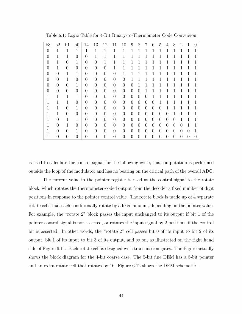
Table 6.1: Logic Table for 4-Bit Binary-to-Thermometer Code Conversion
b3 b2 b1 b0 14 13 12 11 10 9 8 7 6 5 4 3 2 1 00 1 1 1 1 1 1 1 1 1 1 1 1 1 1 1 1 1 10 1 1 0 0 1 1 1 1 1 1 1 1 1 1 1 1 1 10 1 0 1 0 0 1 1 1 1 1 1 1 1 1 1 1 1 10 1 0 0 0 0 0 1 1 1 1 1 1 1 1 1 1 1 10 0 1 1 0 0 0 0 1 1 1 1 1 1 1 1 1 1 10 0 1 0 0 0 0 0 0 1 1 1 1 1 1 1 1 1 10 0 0 1 0 0 0 0 0 0 1 1 1 1 1 1 1 1 10 0 0 0 0 0 0 0 0 0 0 1 1 1 1 1 1 1 11 1 1 1 0 0 0 0 0 0 0 0 1 1 1 1 1 1 11 1 1 0 0 0 0 0 0 0 0 0 0 1 1 1 1 1 11 1 0 1 0 0 0 0 0 0 0 0 0 0 1 1 1 1 11 1 0 0 0 0 0 0 0 0 0 0 0 0 0 1 1 1 11 0 1 1 0 0 0 0 0 0 0 0 0 0 0 0 1 1 11 0 1 0 0 0 0 0 0 0 0 0 0 0 0 0 0 1 11 0 0 1 0 0 0 0 0 0 0 0 0 0 0 0 0 0 11 0 0 0 0 0 0 0 0 0 0 0 0 0 0 0 0 0 0
is used to calculate the control signal for the following cycle, this computation is performed
outside the loop of the modulator and has no bearing on the critical path of the overall ADC.
The current value in the pointer register is used as the control signal to the rotate
block, which rotates the thermometer-coded output from the decoder a fixed number of digit
positions in response to the pointer control value. The rotate block is made up of 4 separate
rotate cells that each conditionally rotate by a fixed amount, depending on the pointer value.
For example, the “rotate 2” block passes the input unchanged to its output if bit 1 of the
pointer control signal is not asserted, or rotates the input signal by 2 positions if the control
bit is asserted. In other words, the “rotate 2” cell passes bit 0 of its input to bit 2 of its
output, bit 1 of its input to bit 3 of its output, and so on, as illustrated on the right hand
side of Figure 6.11. Each rotate cell is designed with transmission gates. The Figure actually
shows the block diagram for the 4-bit coarse case. The 5-bit fine DEM has a 5-bit pointer
and an extra rotate cell that rotates by 16. Figure 6.12 shows the DEM schematics.
44

From Decoder
Adder
Ptr Reg
Rotate 1
Rotate 2
Rotate 4
Rotate 8
To DAC
From ReQ P0
P1
P2
P3
4
4
15In Position Out Position
131415
2345
15 0 1
131415
0123
0123
P1=0 P1=1
Figure 6.11: Block Diagram of DEM Circuitry
6.2 Circuit Simulations
The target clock rate for this design is 50 MHz. Due to the design used for the two-
step quantizer and integrators, the computations in the digital feedback must be completed
during one-half clock cycle. This requires a worst-case delay of less than 10 ns. The “feedback
path” includes the encoder blocks, the ReQ, the decode blocks, and the DEM logic. (A small
amount of extra time must be allotted for the comparators in the internal quantizer at the
beginning and the DACs at the end, so the actual time available is less than 10 ns.) The
critical path for the digital feedback involves the following: a 4-bit bubble decode, a 4-bit
thermometer code-to-binary encoder, an 8-bit adder and a 5-bit adder in the ReQ block,
a 5-bit binary-to-thermometer decoder, and a 31-line DEM consisting of 5 stages of pass
gates. Achieving a transistor-level simulation in which all of these elements operated in the
worst-case condition proved to be very difficult, as the resulting output from a worst-case
simulation of some blocks did not allow for the worst-case simulation of connected blocks.
To simulate an absolute maximum delay, simulations were run on each block separately,
carefully loading each block to mimic its connected operation. Figures 6.13, 6.14, 6.15, 6.16,
and 6.17 show timing diagrams for each of the blocks in the critical path, and Table 6.2
shows the overall results of these simulations. The overall delay should be acceptable; more
45

vdd gnd
gnd
vdd
vdd
vdd
vdd
vdd
gnd
gnd
gnd
gnd
clk2
clk1
gndvdd
sel
GNDVDD
gndvdd
gndvdd
gndvdd
fine_
out<
30:0
>ou
t<30
:0>
rot_
1_31
_bit
in<3
0:1>
sel_
bar
rot_
31_c
ont<
0>
rot_
31_c
ont_
bar<
0>
out<
30:0
>ro
t_2_
31_b
it
in<3
0:0>
sel
sel_
bar
rot_
31_c
ont<
1>
rot_
31_c
ont_
bar<
1>
out<
30:0
>
in<3
0:0>
sel
sel_
bar
rot_
4_31
_bit
rot_
31_c
ont<
2>
rot_
31_c
ont_
bar<
2>
out<
30:0
>
in<3
0:0>
sel
sel_
bar
rot_
8_31
_bit
rot_
31_c
ont<
3>
rot_
31_c
ont_
bar<
3>
gndvdd
out<
30:0
>
in<3
0:0>
sel
sel_
bar
rot_
16_3
1_bi
tro
t_31
_con
t<4>
rot_
31_c
ont_
bar<
4>
fine_
th<3
0:0>
fine_
bin<
4:0>
rot_
31_c
ont<
4:0>
A<4
:0>
B<4
:0>
adde
r_5b
Ove
rflow
Sum
<4:0
>
vdd
gnd
clk2
gnd
vdd
clk1
clk1
clk2
D<4
:0>
d-re
gist
er_5
b
Q<4
:0>
Q_b
ar<4
:0>
rot_
31_c
ont<
4:0>
rot_
31_c
ont_
bar<
4:0>
coar
se_o
ut<1
5:0>
vdd gndgndvdd
out<
15:0
>ro
t_1_
16_b
it
in<1
5:0>
sel
sel_
bar
rot_
16_c
ont<
0>
rot_
16_c
ont_
bar<
0>
vdd gndgndvdd
out<
15:0
>ro
t_2_
16_b
it
in<1
5:0>
sel
sel_
bar
rot_
16_c
ont<
1>
rot_
16_c
ont_
bar<
1>
vdd gndgndvdd
out<
15:0
>ro
t_4_
16_b
it
in<1
5:0>
sel
sel_
bar
rot_
16_c
ont<
2>
rot_
16_c
ont_
bar<
2>
vdd gndgndvdd
out<
15:0
>ro
t_8_
16_b
it
in<1
5:0>
sel
sel_
bar
rot_
16_c
ont<
3>
rot_
16_c
ont_
bar<
3>
vdd,
coa
rse_
th<1
4:0>
coar
se_t
h<14
:0>
vdd
gnd
coar
se_b
in<3
:0>
vdd gndGNDVDD
rot_
16_c
ont<
3:0>
A<3
:0>
B<3
:0>
adde
r_4b
Ove
rflow
Sum
<3:0
>
vdd
gnd
clk2
gnd
vdd
clk1
clk1
clk2
D<3
:0>
d-re
gist
er_4
b
Q<3
:0>
Q_b
ar<3
:0>
rot_
16_c
ont<
3:0>
rot_
16_c
ont_
bar<
3:0>
Figure 6.12: DEM Circuitry
46

Table 6.2: Timing Results for the Critical Path
Block Equivalent Worst-Name Fan Out Case Delay
1) Bubble Decode 1 inverter 0.15 ns2) Therm-to-Bin Encoder 8 inverters 0.23 ns3) 8-bit Subtractor 25 inverters 1.94 ns4) 5-bit Subtractor 35 inverters 1.46 ns5) Bin-to-Therm Decoder 5 layers of muxes
and 31-line DEM and 2 inverters 2.50 ns
TOTAL: ∼ 6.28 ns
simulations that take into account delays of the analog components involved are needed to
thoroughly verify this.
6.3 Conclusion
The circuits presented in this chapter are basic circuit designs such as one could find
in basic textbooks. A few blocks, such as the decoders, were done as complex logic gates
using basic design methods. The design has an overall worst-case delay of under 7 ns, which
is less than the maximum allowable delay of 10 ns.
47
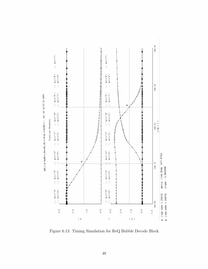
AD
C_
li
b
bu
bb
le
_d
ec
od
e_
4b
_t
im
in
g
sc
he
ma
ti
c
:
Oc
t
30
1
6:
07
:3
2
20
03
Tr
an
si
en
t
Re
sp
on
se
-1
.0
0
.0
1
.0
2
.0
3
.0
16
0.
0n
16
0.
1n
16
0.
2n
16
0.
3n
16
0.
4n
0
.0
1
.0
2
.0
3
.0
:b
it
="
14
":
bi
t=
"1
3"
:b
it
="
12
":
bi
t=
"1
1"
:b
it
="
10
":
bi
t=
"9
";
:b
it
="
8"
;:
bi
t=
"7
";
:b
it
="
6"
;:
bi
t=
"5
";
:b
it
="
4"
;:
bi
t=
"3
";
:b
it
="
2"
;:
bi
t=
"1
";
:b
it
="
0"
;
:b
it
="
14
":
bi
t=
"1
3"
:b
it
="
12
":
bi
t=
"1
1"
:b
it
="
10
":
bi
t=
"9
";
:b
it
="
8"
;:
bi
t=
"7
";
:b
it
="
6"
;:
bi
t=
"5
";
:b
it
="
4"
;:
bi
t=
"3
";
:b
it
="
2"
;:
bi
t=
"1
";
:b
it
="
0"
;
ti
me
(
s
)
( V )( V )
A
B
A:
(
16
0.
10
4n
1
.2
50
15
)d
el
ta
:
(1
44
.8
34
p
-4
17
.4
15
u)
B:
(
16
0.
24
9n
1
.2
49
73
)s
lo
pe
:
-2
.8
82
04
M
Figure 6.13: Timing Simulation for ReQ Bubble Decode Block
48

AD
C_
li
b
en
c_
th
er
m_
to
_b
in
_4
_b
it
_2
s_
ti
mi
ng
s
ch
em
at
ic
:
O
ct
3
0
16
:2
0:
55
2
00
3
Tr
an
si
en
t
Re
sp
on
se
-1
.0
0
.0
1
.0
2
.0
3
.0
9.
90
n1
0.
0n
10
.1
n1
0.
2n
10
.3
n1
0.
4n
-1
.0
0
.0
1
.0
2
.0
3
.0
:b
it
="
3"
;/
ou
tp
ut
<3
:0
>:
bi
t=
"2
";
/o
ut
pu
t<
3:
0>
:b
it
="
1"
;/
ou
tp
ut
<3
:0
>:
bi
t=
"0
";
/o
ut
pu
t<
3:
0>
:b
it
="
1:
bi
t=
"1
:b
it
="
1:
bi
t=
"1
:b
it
="
1:
bi
t=
"9
:b
it
="
8:
bi
t=
"7
:b
it
="
6:
bi
t=
"5
:b
it
="
4:
bi
t=
"3
:b
it
="
2:
bi
t=
"1
:b
it
="
0
ti
me
(
s
)
( V )( V )
A
B
A:
(
10
.0
49
3n
1
.2
56
99
)d
el
ta
:
(2
25
.8
26
p
70
.0
47
8u
)B
:
(1
0.
27
51
n
1.
25
70
6)
sl
op
e:
3
10
.1
84
K
Figure 6.14: Timing Simulation for ReQ Encoder Block
49
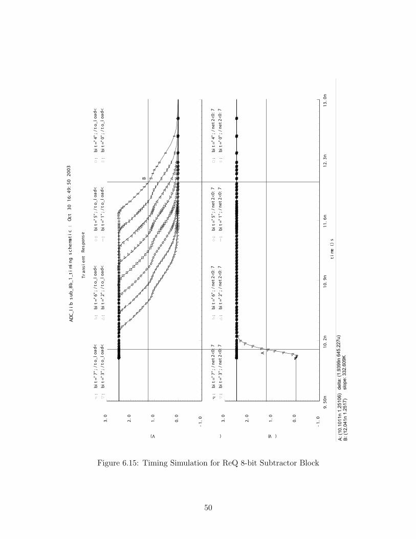
AD
C_
li
b
su
b_
8b
_1
_t
im
in
g
sc
he
ma
ti
c
:
Oc
t
30
1
6:
49
:5
0
20
03
Tr
an
si
en
t
Re
sp
on
se
-1
.0
0
.0
1
.0
2
.0
3
.0
9.
50
n1
0.
2n
10
.9
n1
1.
6n
12
.3
n1
3.
0n
-1
.0
0
.0
1
.0
2
.0
3
.0
:b
it
="
7"
;/
ne
t2
<0
:7
:b
it
="
6"
;/
ne
t2
<0
:7
:b
it
="
5"
;/
ne
t2
<0
:7
:b
it
="
4"
;/
ne
t2
<0
:7
:b
it
="
3"
;/
ne
t2
<0
:7
:b
it
="
2"
;/
ne
t2
<0
:7
:b
it
="
1"
;/
ne
t2
<0
:7
:b
it
="
0"
;/
ne
t2
<0
:7
:b
it
="
7"
;/
to
_l
oa
d<
:b
it
="
6"
;/
to
_l
oa
d<
:b
it
="
5"
;/
to
_l
oa
d<
:b
it
="
4"
;/
to
_l
oa
d<
:b
it
="
3"
;/
to
_l
oa
d<
:b
it
="
2"
;/
to
_l
oa
d<
:b
it
="
1"
;/
to
_l
oa
d<
:b
it
="
0"
;/
to
_l
oa
d<
ti
me
(
s
)
( V )( V )
A
B
A: (
10.1
011n
1.2
5106
)�de
lta: (
1.93
99n
645.
227u
)B
: (12
.041
n 1.
2517
)�
slo
pe: 3
32.6
09K
Figure 6.15: Timing Simulation for ReQ 8-bit Subtractor Block
50
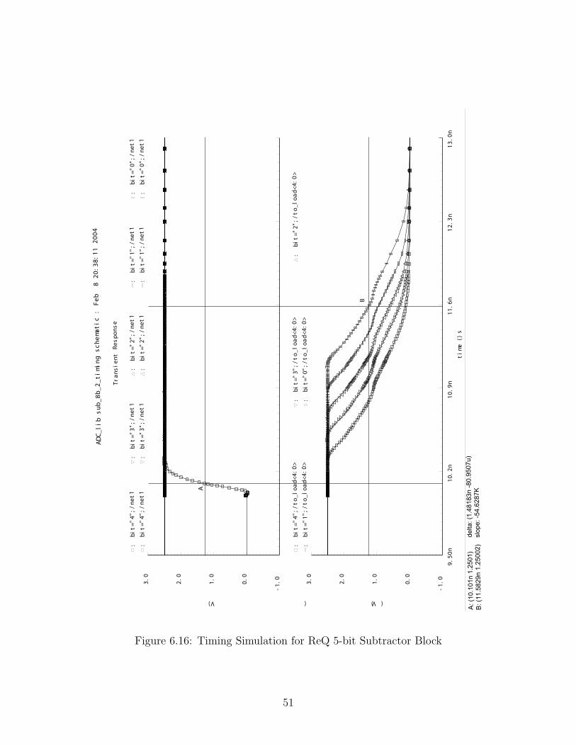
AD
C_
li
b
su
b_
8b
_2
_t
im
in
g
sc
he
ma
ti
c
:
Fe
b
8
2
0:
38
:1
1
20
04
Tr
an
si
en
t
Re
sp
on
se
-1
.0
0
.0
1
.0
2
.0
3
.0
9.
50
n1
0.
2n
10
.9
n1
1.
6n
12
.3
n1
3.
0n
-1
.0
0
.0
1
.0
2
.0
3
.0
:b
it
="
4"
;/
to
_l
oa
d<
4:
0>
:b
it
="
3"
;/
to
_l
oa
d<
4:
0>
:b
it
="
2"
;/
to
_l
oa
d<
4:
0>
:b
it
="
1"
;/
to
_l
oa
d<
4:
0>
:b
it
="
0"
;/
to
_l
oa
d<
4:
0>
:b
it
="
4"
;/
ne
t1
:b
it
="
3"
;/
ne
t1
:b
it
="
2"
;/
ne
t1
:b
it
="
1"
;/
ne
t1
:b
it
="
0"
;/
ne
t1
:b
it
="
4"
;/
ne
t1
:b
it
="
3"
;/
ne
t1
:b
it
="
2"
;/
ne
t1
:b
it
="
1"
;/
ne
t1
:b
it
="
0"
;/
ne
t1
ti
me
(
s
)
( V )( V )
A
B
A: (
10.1
01n
1.25
01)�
d
elta
: (1.
4818
3n -8
0.95
07u)
B: (
11.5
829n
1.2
5002
)� s
lope
: -54
.628
7K
Figure 6.16: Timing Simulation for ReQ 5-bit Subtractor Block
51
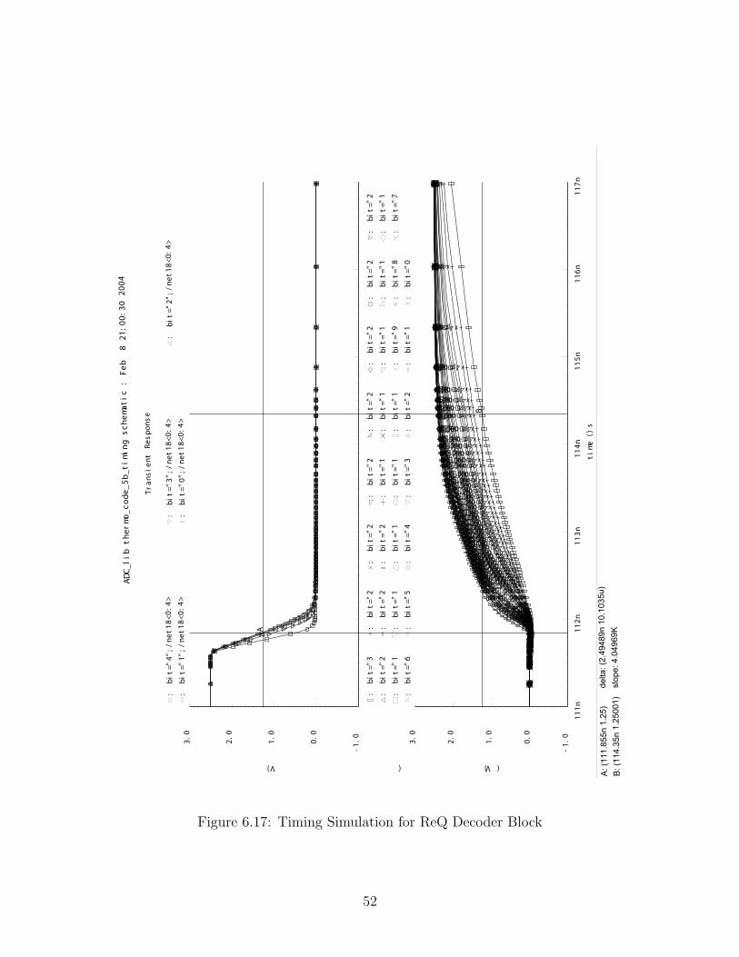
AD
C_
li
b
th
er
mo
_c
od
e_
5b
_t
im
in
g
sc
he
ma
ti
c
:
Fe
b
8
2
1:
00
:3
0
20
04
Tr
an
si
en
t
Re
sp
on
se
-1
.0
0
.0
1
.0
2
.0
3
.0
11
1n
1
12
n
11
3n
1
14
n
11
5n
1
16
n
11
7n
-1
.0
0
.0
1
.0
2
.0
3
.0
:b
it
="
3:
bi
t=
"2
:b
it
="
2:
bi
t=
"2
:b
it
="
2:
bi
t=
"2
:b
it
="
2:
bi
t=
"2
:b
it
="
2:
bi
t=
"2
:b
it
="
2:
bi
t=
"1
:b
it
="
1:
bi
t=
"1
:b
it
="
1:
bi
t=
"1
:b
it
="
1:
bi
t=
"1
:b
it
="
1:
bi
t=
"1
:b
it
="
1:
bi
t=
"9
:b
it
="
8:
bi
t=
"7
:b
it
="
6:
bi
t=
"5
:b
it
="
4:
bi
t=
"3
:b
it
="
2:
bi
t=
"1
:b
it
="
0
:b
it
="
4"
;/
ne
t1
8<
0:
4>
:b
it
="
3"
;/
ne
t1
8<
0:
4>
:b
it
="
2"
;/
ne
t1
8<
0:
4>
:b
it
="
1"
;/
ne
t1
8<
0:
4>
:b
it
="
0"
;/
ne
t1
8<
0:
4>
ti
me
(
s
)
( V )( V )
A
B
A: (
111.
855n
1.2
5)�
d
elta
: (2.
4948
9n 1
0.10
35u)
B: (
114.
35n
1.25
001)
� s
lope
: 4.0
4969
K
Figure 6.17: Timing Simulation for ReQ Decoder Block
52

Chapter 7
Conclusion
7.1 Contributions
The intended contributions of this research are as follows:
• A new presentation and mathematical analysis of the problems involved with segment-
ing the digital word in a ∆Σ ADC feedback path.
• Design of two potential methods to overcome these problems: a calibration method
and a requantization method.
• Simulations for these two potential solutions, along with an analysis and comparison.
• Designs for the circuits of the ReQ method to be used with a 50 MHz ∆Σ ADC design
with 8-bit internal quantization and a desired output resolution of over 15 bits, along
with timing and functional simulations.
A paper presenting this work has been accepted for publication at the 2004 IEEE
International Symposium on Circuits and Systems [15].
7.2 Summary of Results
Chapter 3 presented that segmentation of the DAC structures in the feedback path
of ∆Σ ADCs is desirable. It simplifies circuitry and allows for higher levels of internal
quantization. However, the mismatch between the two DAC banks adds an additional source
of error to the system, significantly reducing the effective SNR of the overall modulator. Two
potential solutions were proposed: one to calibrate the DAC banks and remove the mismatch,
53

and the other to requantize the segmented signals and frequency shape the error resulting
from the mismatch away from the band of interest.
The calibration method described in Chapter 4 adds no extra logic to the feedback
path of the ∆Σ ADC, insuring that the feedback path does not limit the overall clock speed.
It does, however, add an initialization routine to set the calibration values, which must be
run before regular operation can occur. This calibration routine must calibrate the DACs
for each stage of the ∆Σ modulator, increasing the time required to perform calibration for
high-order modulators. In the test case of a second-order modulator with an OSR of 20,
an internal quantization of (4+4)-bit, and the coarse and fine percent mismatches scaled
assuming a 16:1 size ratio between coarse and fine elements, the calibration method achieves
an average SNR of 98dB at a mismatch of 1%. This is only 0.5dB less than the SNR of the
full 8-bit DEM reference case.
The ReQ method described in Chapter 5 does add logic to the feedback path, but it
requires no initialization or startup routine. The critical path through the required logic is
fairly short, and can be optimized to limit the effect of the feedback path logic on the overall
clock speed. The DC offset inserted by the ReQ logic can be removed by a small change in
the DAC structure, and the overall SNR of this method is acceptable, if a little worse than
that of the calibration method. In the standard test case at 1% fine element mismatch, the
ReQ method achieves an average SNR of about 96dB, which is only 2dB less than the SNR
of the full 8-bit DEM reference case.
The ReQ method scales better for use with higher-order modulators. It also has fewer
implementation-related random factors to influence its actual operation in silicon, as it is
completely digital. For these reasons, it is the chosen method to use for the specific ∆Σ
design. The circuits were designed (discussed in Chapter 6, and shown in full in Appendix
A) to minimize power consumption while still meeting the timing goals. The total delay
achieved through the feedback path was about 7 ns.
7.3 Areas for Potential Future Research
Some areas of suggested research on the material presented in this thesis are:
54

• Further develop and verify the analysis of the DC offset introduced by the ReQ method.
More specifically identify its source and how to avoid or more completely remove it,
preferably using a digital method.
• Adapt a higher-order DEM algorithm that does not introduce significant additionally
delay for use in the ADC. This would permit the use of a higher-order ReQ circuit and
provide higher output resolution.
• Expand existing background calibration methods that calibrate DAC elements into one
which will provide background calibration between the coarse and fine banks [14].
• Further optimize the digital circuitry of the ∆Σ feedback path. This includes higher-
order or more efficient methods of performing the ReQ modulation, as well as more
efficient circuits to implement all functions.
55

Appendix
56

Appendix A
Complete Circuit Schematics
A.1 Top Level Schematic
I6
I7 I5
I4
I3
I2
I1I0
bubble_decode_4b
bubble_decode_4b
enc_therm_to_bin_4_bit_2s
enc_therm_to_bin_4_bit
thermo_code_convert_5b
thermo_code_convert_4b
DEMReQ
fine<15:1>
coarse<15:1>
yc<7:4>,yf<3:0>
yf<3:0>
vdd
gnd
gnd
vdd
vdd
gnd
gnd
vdd
yc<7:4>
clk2
clk1
clk2
clk1 vdd
gnd
gnd
gnd
vdd
vdd
gnd
vdd
zf<4:0>
zc<3:0>
zf<4:0>
zc<3:0>
coarse_DAC_bar<15:0>
fine<15:1>
vdd
fine_DAC_bar<30:0>
gnd
clk2
clk1
coarse<15:1>
gnd
vdd
one_high<15:1>TC<15:1>
gnd
vdd
one_high<15:1>TC<15:1>
gnd
vddbit<3:0>one_high<15:1>
gnd
vddbit<3:0>one_high<15:1>
gnd
vdd
TC_bar<30:0>b<4:0>
gnd
vdd
TC_bar<14:0>b<3:0>
clk2clk1gnd
vddcoarse_out<15:0>
fine_out<30:0>
coarse_bin<3:0>
coarse_th<14:0>
fine_bin<4:0>
fine_th<30:0>
gnd
vdd
coarse<7:4>
fine<4:0>
clk1
clk2
in<7:0>
Figure A.1: Overall Schematic for Digital Feedback Path
57

A.2 Bubble Decode
I34
I31
I32
I29
I28
I33
I27
I26
I25
I24
I23
I22
I21
I20
I19
I18
I17
I16
I15
I14
I13
I12
I11
I9
I8
I7
I6
I5
I4
I3
I2
I1
I0
gnd
vdd
gnd
vdd
gnd
vdd
gnd
vdd
gnd
vdd
gnd
vdd
gnd
vdd
gnd
vdd
gnd
vdd
gnd
vdd
gnd
vdd
gnd
vdd
gnd
vdd
gnd
vdd
gnd
vdd
gnd
vdd
gnd
vdd
gnd
vdd
gnd
vdd
Q
A
B
C
gnd
vdd
Q
A
B
C
gnd
vdd
Q
A
B
C
gnd
vdd
Q
A
B
C
gnd
vdd
Q
A
B
C
gnd
vdd
Q
A
B
C
gnd
vdd
Q
A
B
C
gnd
vdd
Q
A
B
C
gnd
vdd
Q
A
B
C
gnd
vdd
Q
A
B
C
gnd
vdd
Q
A
B
C
gnd
vdd
Q
A
B
C
gnd
vdd
Q
A
B
C
gnd
vdd
Q
A
B
C
gnd
vdd
Q
A
B
C
vdd
gnd
TC<15:1>
one_high<15:1>
TC<15> in
vdd
gnd
inverter_1b
out
TC<14> in
vdd
gnd
inverter_1b
out
TC<13> invd
dgn
d
inverter_1b
out
TC<14> in
vdd
gnd
inverter_1b
out
TC<13> in
vdd
gnd
inverter_1b
out
TC<15>
TC<15>
TC<14>
TC<13> in
vdd
gnd
inverter_1b
out
TC<14>
TC<13>
TC<12> in
vdd
gnd
inverter_1b
out
TC<13>
TC<12>
TC<11> in
vdd
gnd
inverter_1b
out
TC<12>
TC<11>
TC<10> in
vdd
gnd
inverter_1b
out
TC<11>
TC<10>
TC<9> in
vdd
gnd
inverter_1b
out
one_high<15>NOR3
vdd
gnd
one_high<14>NOR3
vdd
gnd
one_high<13>NOR3
vdd
gnd
one_high<12>NOR3
vdd
gnd
one_high<11>NOR3
vdd
gnd
one_high<10>NOR3
vdd
gnd
one_high<9>NOR3
vdd
gnd
TC<3>
TC<2>
TC<1> in
vdd
gnd
inverter_1b
out
one_high<1>NOR3
vdd
gnd
TC<4>
TC<3>
TC<2> in
vdd
gnd
inverter_1b
out
one_high<2>NOR3
vdd
gnd
TC<5>
TC<4>
TC<3> in
vdd
gnd
inverter_1b
out
one_high<3>NOR3
vdd
gnd
TC<6>
TC<5>
TC<4> invd
dgn
d
inverter_1b
out
one_high<4>NOR3
vdd
gnd
TC<7>
TC<6>
TC<5> in
vdd
gnd
inverter_1b
out
one_high<5>NOR3
vdd
gnd
TC<8>
TC<7>
TC<6> in
vdd
gnd
inverter_1b
out
one_high<6>NOR3
vdd
gnd
TC<9>
TC<8>
TC<7> in
vdd
gnd
inverter_1b
out
one_high<7>NOR3
vdd
gnd
TC<10>
TC<9>
TC<8> in
vdd
gnd
inverter_1b
out
one_high<8>NOR3
vdd
gnd
Figure A.2: Bubble Decode Logic
58
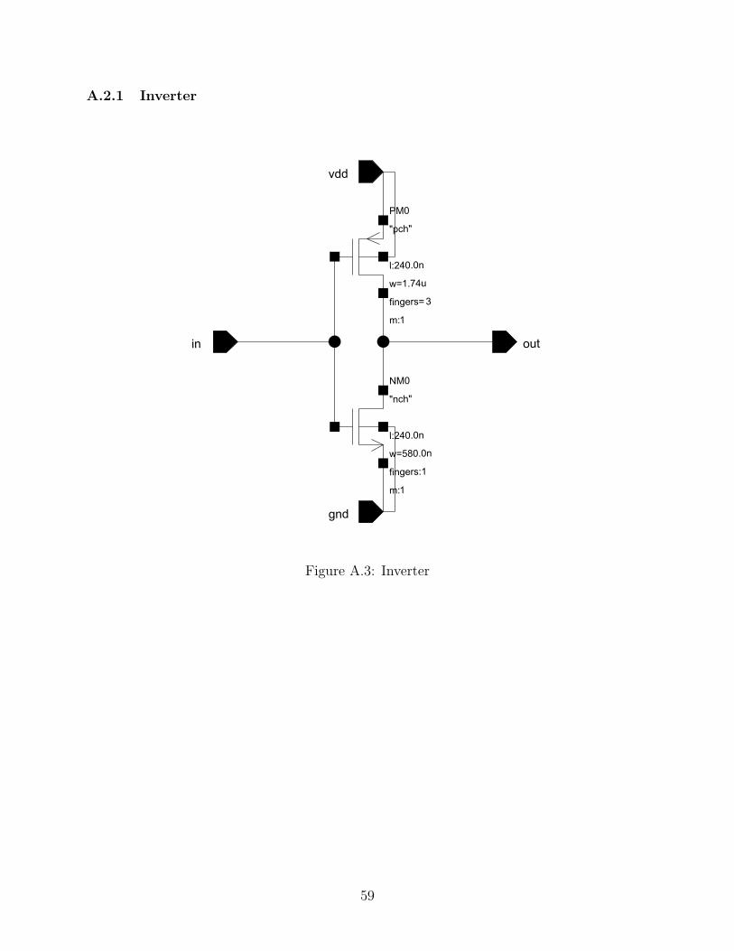
A.2.1 Inverter
l:240.0n
w=580.0n
"nch"
fingers:1
m:1
m:1
"pch"
w=1.74u
l:240.0n
fingers= 3
NM0
PM0
vdd
in
gnd
out
Figure A.3: Inverter
59

A.2.2 3 Input Nor
gnd
C
Q
vdd
CA
B
B
vdd
vdd
vdd
A
gndgnd gnd
B
C
vdd
gnd
A
Q
P-type devices:l=240nw=5.22u
N-type devices:l=240nw=580n
Figure A.4: Nor Gate
60

A.3 2’s Complement Encoder
l :240.0n
w=1.16u
"nch"
fingers:1
m:1
l:240.0n
w=1.16u
"nch"
fingers:1
m:1
l:240.0n
w=1.16u
"nch"
fingers:1
m:1
l:240.0n
w=1.16u
"nch"
fingers:1
m:1
l:240.0n
w=580.0n
"nch"
fingers:1
m:1
l:240.0n
w=580.0n
"nch"
fi ngers:1
m:1
l:240.0n
w=580.0n
"nch"
fingers:1
m:1
l:240.0n
w=580.0n
"nch"
fingers:1
m:1
l:240.0n
w=580.0n
"nch"
fingers:1
m:1
l:240.0n
w=580.0n
"nch"
fingers:1
m:1
l :240.0n
w=580.0n
"nch"
fingers:1
m:1
l:240.0n
w=580.0n
"nch"
fingers:1
m:1
l:240.0n
w=580.0n
"nch"
fingers:1
m:1
l:240.0n
w=580.0n
"nch"
fingers:1
m:1
l:240.0n
w=580.0n
"nch"
fingers:1
m:1
l:240.0n
w=580.0n
"nch"
fingers:1
m:1
l:240.0n
w=580.0n
"nch"
fingers:1
m:1
l:240.0n
w=580.0n
"nch"
fingers:1
m:1
l:240.0n
w=580.0n
"nch"
fingers:1
m:1
l:240.0n
w=580.0n
"nch"
fingers:1
m:1
l:240.0n
w=580.0n
"nch"
fingers:1
m:1
l:240.0n
w=580.0n
"nch"
fingers:1
m:1
l:240.0n
w=580.0n
"nch"
fingers:1
m:1
l:240.0n
w=580.0n
"nch"
fingers:1
m:1
l:240.0n
w=580.0n
"nch"
fingers:1
m:1
l:240.0n
w=580.0n
"nch"
fingers:1
m:1
l:240.0n
w=580.0n
"nch"
fingers:1
m:1
l:240.0n
w=580.0n
"nch"
fingers:1
m:1
l:240.0n
w=580.0n
"nch"
fingers:1
m:1
l:240.0n
w=580.0n
"nch"
fingers:1
m:1
l:240.0n
w=580.0n
"nch"
fingers:1
m:1
l:240.0n
w=580.0n
"nch"
fingers:1
m:1
l:240.0n
w=580.0n
"nch"
fingers:1
m:1
l:240.0n
w=580.0n
"nch"
fingers:1
m:1
l:240.0n
w=580.0n
"nch"
fingers:1
m:1
l:240.0n
w=580.0n
"nch"
fingers:1
m:1
l:240.0n
w=1.16u
"nch"
fingers:1
m:1
m:1
"pch"
w=1.74u
l:240.0n
fingers=3
m:1
"pch"
w=1.74u
l: 240.0n
fingers=3
m:1
"pch"
w=1.74u
l:240.0n
fingers=3
m:1
"pch"
w=1.74u
l:240.0n
fingers=3
m:1
"pch"
w=580.0n
l:240.0n
fingers:1
m:1
"pch"
w=580.0n
l:240.0n
fingers:1
m:1
"pch"
w=1.74u
l:240.0n
fingers=3
m:1
"pch"
w=580.0n
l:240.0n
fingers:1
m:1
"pch"
w=580.0n
l:240.0n
fingers:1
NM30
NM97
NM31
NM32
NM33NM34NM35NM36
NM37 NM38 NM39
NM43NM44
NM45 NM46 NM48
NM49NM52
NM53
NM58NM60
NM61 NM63 NM64
NM72
NM75
NM77NM78
NM82
NM85NM87
NM90NM91
NM94 NM95 NM96
NM1
PM34
PM37
PM35
PM36
PM32PM30
PM1
PM31 PM33
vdd
bit<2>
vdd
gnd
gnd
vdd
bit<0>
bit<1>
vdd
gnd
one_high<15>
one_high<2>
vdd
gnd
one_high<1>
one_high<5>
one_high<6>
one_high<4>
one_high<3>
one_high<11>
one_high<12>
one_high<13>
one_high<14>
one_high<9>
one_high<10>
one_high<8>
one_high<7>
bit<3>
vdd
gnd
gnd
one_high<15:1>
bit<3:0>
gndvdd
Both N and P type devices in array are w/l=540n/240n.
Inverters are P:w/l=1.74u/240n N:w/l=1.16u/240n.
Figure A.5: 2’s Complement Encoder
61

A.4 Unsigned Encoder
l :240.0n
w=1.16u
"nch"
fingers:1
m:1
l:240.0n
w=1.16u
"nch"
fingers:1
m:1
l:240.0n
w=1.16u
"nch"
fingers:1
m:1
l:240.0n
w=580.0n
"nch"
fingers:1
m:1
l:240.0n
w=580.0n
"nch"
fi ngers:1
m:1
l:240.0n
w=580.0n
"nch"
fingers:1
m:1
l:240.0n
w=580.0n
"nch"
fingers:1
m:1
l:240.0n
w=580.0n
"nch"
fingers:1
m:1
l:240.0n
w=580.0n
"nch"
fingers:1
m:1
l :240.0n
w=580.0n
"nch"
fingers:1
m:1
l:240.0n
w=580.0n
"nch"
fingers:1
m:1
l:240.0n
w=580.0n
"nch"
fingers:1
m:1
l:240.0n
w=580.0n
"nch"
fingers:1
m:1
l:240.0n
w=580.0n
"nch"
fingers:1
m:1
l:240.0n
w=580.0n
"nch"
fingers:1
m:1
l:240.0n
w=580.0n
"nch"
fingers:1
m:1
l:240.0n
w=580.0n
"nch"
fingers:1
m:1
l:240.0n
w=580.0n
"nch"
fingers:1
m:1
l:240.0n
w=580.0n
"nch"
fingers:1
m:1
l:240.0n
w=580.0n
"nch"
fingers:1
m:1
l:240.0n
w=580.0n
"nch"
fingers:1
m:1
l:240.0n
w=580.0n
"nch"
fingers:1
m:1
l:240.0n
w=580.0n
"nch"
fingers:1
m:1
l:240.0n
w=580.0n
"nch"
fingers:1
m:1
l:240.0n
w=580.0n
"nch"
fingers:1
m:1
l:240.0n
w=580.0n
"nch"
fingers:1
m:1
l:240.0n
w=580.0n
"nch"
fingers:1
m:1
l:240.0n
w=580.0n
"nch"
fingers:1
m:1
l:240.0n
w=580.0n
"nch"
fingers:1
m:1
l:240.0n
w=580.0n
"nch"
fingers:1
m:1
l:240.0n
w=580.0n
"nch"
fingers:1
m:1
l:240.0n
w=580.0n
"nch"
fingers:1
m:1
l:240.0n
w=580.0n
"nch"
fingers:1
m:1
l:240.0n
w=580.0n
"nch"
fingers:1
m:1
l:240.0n
w=580.0n
"nch"
fingers:1
m:1
l:240.0n
w=1.16u
"nch"
fingers:1
m:1
m:1
"pch"
w=1.74u
l:240.0n
fingers=3
m:1
"pch"
w=1.74u
l:240.0n
fingers=3
m:1
"pch"
w=1.74u
l:240.0n
fingers=3
m:1
"pch"
w=580.0n
l:240.0n
fingers:1
m:1
"pch"
w=580.0n
l:240.0n
fingers:1
m:1
"pch"
w=1.74u
l:240.0n
fingers=3
m:1
"pch"
w=580.0n
l:240.0n
fingers:1
m:1
"pch"
w=580.0n
l:240.0n
fingers:1
NM30
NM31
NM32
NM33NM34NM35NM36
NM37 NM38 NM39
NM43NM44
NM45 NM46 NM48
NM49NM52
NM53
NM58NM60
NM61 NM63 NM64
NM72
NM75
NM77NM78
NM82
NM85NM87
NM90NM91
NM94 NM95 NM96
NM1
PM34
PM35
PM36
PM32PM30
PM1
PM31 PM33
vdd
bit<2>
vdd
gnd
gnd
vdd
bit<0>
bit<1>
vdd
gnd
one_high<15>
one_high<2>
one_high<1>
one_high<5>
one_high<6>
one_high<4>
one_high<3>
one_high<11>
one_high<12>
one_high<13>
one_high<14>
one_high<9>
one_high<10>
one_high<8>
one_high<7>
vdd
gnd
gnd
one_high<15:1>
bit<3:0>
gndvdd
Both N and P type devices in array are w/l=540n/240n.
Inverters are P:w/l=1.74u/240n N:w/l=1.16u/240n.
bit<3>
Figure A.6: Unsigned Encoder
62

A.5 ReQ
I8
I11
I12
I9
gnd
vdd
<7:0>
GN
D
VD
D
gnd
vdd
GN
D
VD
D
GN
D
VD
D
Sum
<4:0
>
Ove
rflow
A<4
:0>
B<4
:0>
sub_
5b
<4:0
>
coar
se<4
>,gn
d,gn
d,gn
d,gn
d
gnd
vdd
Sum
<7:0
>
Ove
rflow
A<7
:0>
B<7
:0>
sub_
8b
gnd
vdd
in<7
:0>
coar
se<7
:4>,
coar
se<3
:0>
coar
se<7
:4>
coar
se<7
:4>
fine<
4:0>
coar
se<7
:4>,
gnd,
gnd,
gnd,
gnd
gnd
vdd
Sum
<7:0
>
Ove
rflow
A<7
:0>
B<7
:0>
sub_
8b
clk1
clk2
d-re
gist
er_8
b
Q<7
:0>
D<7
:0>
clk1
clk2
gnd
vdd
Figure A.7: Requantization Logic
63

A.5.1 8-bit Subtractor
inverter_1b
inverter_1b
inverter_1b
inverter_1b
inverter_1b
inverter_1b
inverter_1b
inverter_1b
xor2
GND
VDD
VDD
VDD
VDD
VDD
VDD
VDD
VDD
VDD
VDD
VDD
VDD
VDD
VDD
VDD
GND
GND
GND
GND
GND
GND
GND
GND
GND
B<1>
B<2>
B<3>
B<4>
B<5>
B<6>
Sum<3>
Sum<2>
GND
GND
B<0>
B<7>
GND
Sum<4>
Sum<5>
GND
GND
GND
VDD
Sum<1>
Sum<7>
Sum<0>
Sum<6>
GND
VDD
VD
D
A<0>
A<1>
A<2>
A<3>
A<4>
A<5>
A<6>
A<7>
Ove
rflow
GN
D
VD
D
Sum
<7:0
>
gnd
vdd
outin
gnd
vdd
outin
gnd
vdd
outin
gnd
vdd
outin
gnd
vdd
outin
gnd
vdd
outin
gnd
vdd
outin
gnd
vdd
outin
gndvd
d
out
A B
GNDVDD
SumB
A
GNDVDD
SumB
A
GNDVDD
SumB
A
GNDVDD
Sum
Cou
t
B
A
GNDVDD
SumB
A
GNDVDD
SumB
A
GNDVDD
SumB
A
GNDVDD
SumB
A
Full
Add
erFu
ll A
dder
Cou
tC
inFu
ll A
dder
Cou
tC
inFu
ll A
dder
Cou
tC
inFu
ll A
dder
Cou
tC
inFu
ll A
dder
Cou
tC
inFu
ll A
dder
Cou
tC
inFu
ll A
dder
Cou
tC
inC
in
B<7
:0>
A<7
:0>
Figure A.8: 8-bit Subtractor
64
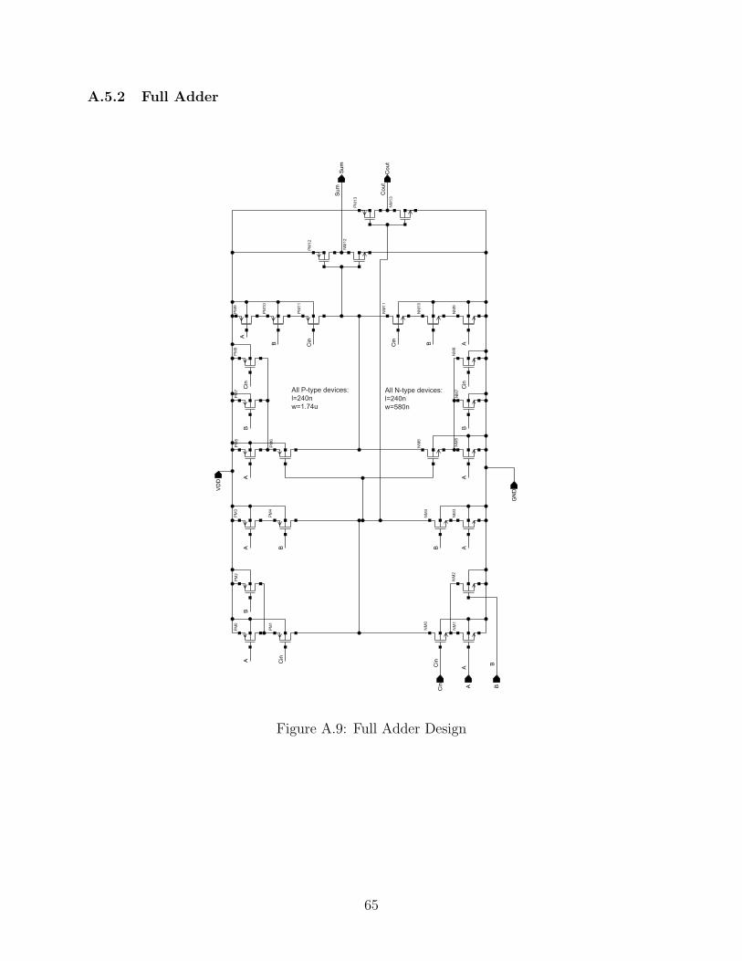
A.5.2 Full Adder
Sum Cou
t
A
B Cin
Cin
BA
BAB
CinA
Cin B A
AA
ACin
Cin
B
B
B
VD
D
GN
D
Cou
t
Sum
Cin BA
PM0
PM1
PM2
NM
0
NM
1N
M2
NM
4
NM
3
PM
3
PM
4
PM
5
PM
6
PM
7P
M8
NM
5
NM
6
NM
7N
M8
PM
10
PM
9
PM
11
NM
11
NM
10
NM
9
NM
12
PM
12
PM
13
NM
13All P-type devices:l=240nw=1.74u
All N-type devices:l=240nw=580n
Figure A.9: Full Adder Design
65

A.5.3 5-bit Subtractor
Full
Add
erFu
ll A
dder
Full
Add
erFu
ll A
dder
Full
Add
er
inverter_1b
inverter_1b
inverter_1b
inverter_1b
inverter_1b
xor2
GND
VDD
VDD
VDD
VDD
VDD
VDD
VDD
VDD
VDD
VDD
GND
GND
GND
GND
GND
GND
B<1>
B<2>
B<3>
B<4>
Sum<3>
Sum<2>
GND
B<0>
GND
Sum<4>
GND
Sum<1>
Sum<0>
GND
VDD
VD
D
A<0>
A<1>
A<2>
A<3>
A<4>
Sum
<4:0
>
B<4
:0>
Ove
rflow
GN
D
VD
D
A<4
:0>
gnd
vdd
outin
gnd
vdd
outin
gnd
vdd
outin
gnd
vdd
outin
gnd
vdd
outin
gndvd
d
out
A B
GNDVDD
SumC
out
Cin
B
A
GNDVDD
Sum
Cou
tC
in
B
A
GNDVDD
Sum
Cou
tC
in
B
A
GNDVDD
Sum
Cou
tC
in
B
A
GNDVDD
Sum
Cou
tC
in
B
A
Figure A.10: 5-bit Subtractor
66

A.5.4 D-Register Bank
gnd
vdd
gnd
vdd
QD
gnd
vdd
QD
gnd
vdd
QD
gnd
vdd
QD
gnd
vdd
QD
gnd
vdd
QD
gnd
vdd
QD
gnd
vdd
QD
clk1 clk1
clk1 clk1
clk1clk1
clk1 clk1
clk1clk1
clk1clk1
clk1clk1
clk1clk1
clk2clk2
clk2clk2
clk2clk2
clk2clk2
clk2 clk2
clk2 clk2
clk2clk2
clk2clk2
d-register
d-register
d-register
d-register
d-register
d-register
d-register
d-registerQ_bar
Q_bar
Q_bar
Q_bar
Q_bar
Q_bar
Q_bar
Q_bar
clk1
clk2
D<7:0> Q<7:0>
Q<7>
Q<6>
Q<4>
Q<5>
Q<1>
Q<2>
Q<3>
Q<0>
D<7>
D<5>
D<6>
D<2>
D<3>
D<4>
D<1>
D<0>
Figure A.11: D-Register Bank
67
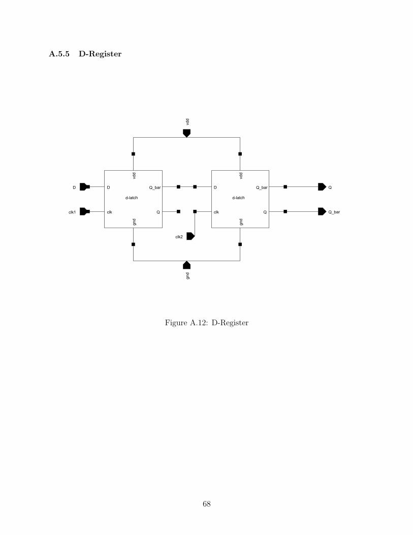
A.5.5 D-Register
d-latchd-latch
gnd
vdd
Q_bar
QD
clk2
clk1
gnd
vdd
Q
Q_barD
clk
gnd
vdd
Q
Q_barD
clk
Figure A.12: D-Register
68
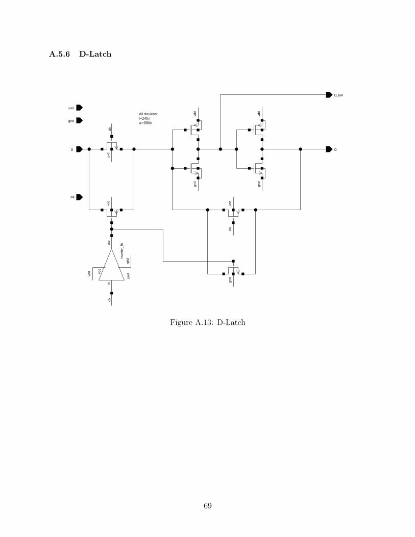
A.5.6 D-Latch
inve
rter_
1b
gnd
gnd
vdd
gnd
vdd
clk
gnd
gnd
vdd
vdd
vdd
D
Q_bar
Q
vdd
gnd
gndvd
d
out
incl
kcl
k
clk
All devices:l=240nw=580n
Figure A.13: D-Latch
69
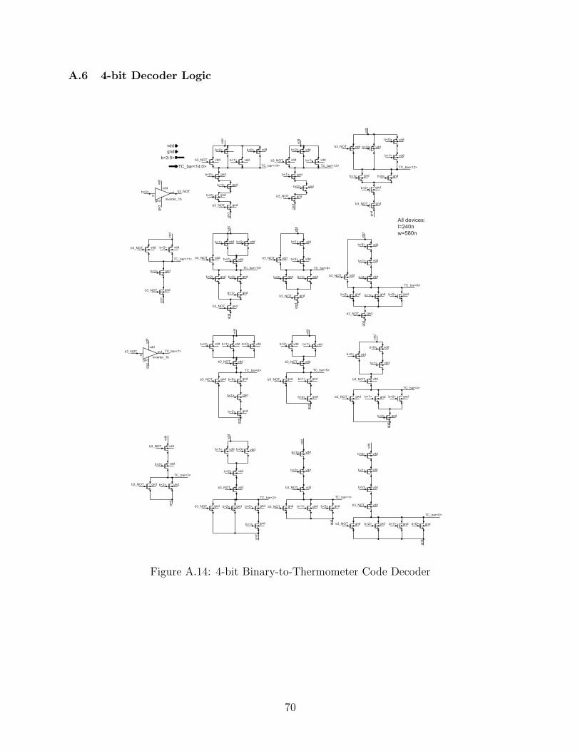
A.6 4-bit Decoder Logic
vdd
vddgnd
b<3:0>
TC_bar<14:0>
vdd
vdd
vdd vdd
vdd
vdd vdd
vdd
vdd
vdd vdd
vdd
vdd
vdd
vdd
vdd
vddvdd
vdd
vdd
vdd
vdd
vdd
vddvdd
vdd
vdd
vddvdd
vdd
vdd
vdd
vddvddvdd
vdd
vdd vdd
vdd
vdd
vdd
vdd
vdd
vdd
vdd
vdd
vdd
vdd
vdd
vdd
vdd
vdd
vdd
vdd
vdd
vdd
vdd
vdd
vdd
vdd
vdd
vdd
gnd
gnd
gnd
gnd
gnd
gnd
gnd
gnd
gnd
gnd
gnd
gndgnd
gnd
gnd
gnd
gnd gnd gndgn
dgnd
gndgnd
gnd
gnd
gnd gnd
gnd
gnd gnd
gnd
gnd
gnd
gnd
gndgnd
gnd
gnd
gndgndgnd
gnd
gnd
gnd gnd gnd gndgnd
gndgndgnd
gnd
gnd
gnd gnd gnd
b<0>
b<0>
b<0>
b<0>
b<0>
b<0>
b<0>
b<0>
gnd
gnd
b<0>
b<0>
b<0>
b<0>
b<0>
b<0>
b<0>
b<0>
b<1>
b<1>
b<1>
b<1>
b<1>
b<1>
b<1>
b<1>
b<1>
b<1>
b<1>
b<1>
b<1>
b<1>
b<1>
b<1>
b<1>
b<1>
b<1>
b<1>b<1>
b<1>
b<1>
b<1>
b<2>
b<2>
b<2>
b<2>b<2>
b<2>
b<2>
b<2>
b<2>
b<2>
b<2>
b<2>
b<2>
b<2> gnd
gnd
gnd
b<2>
b<2>
b<2>
b<2>
b<2>
b<2>
b<2>
b<2>
b<2>
b<2>b<2>
b<2>
b<2>
b<2>gnd gnd
gnd
TC_bar<14> TC_bar<13> TC_bar<12>
TC_bar<8>
TC_bar<9>TC_bar<10>
TC_bar<11>
TC_bar<7>
TC_bar<6>
TC_bar<4>
TC_bar<5>
TC_bar<0>
TC_bar<1>TC_bar<2>
TC_bar<3>
inverter_1b
outin
All devices:l=240nw=580n
vdd
gnd
vdd
gnd inverter_1b
outin
b<3> b3_NOT
b3_NOT
b3_NOT
b3_NOT
b3_NOT
b3_NOT
b3_NOT
b3_NOT
b3_NOT
b3_NOT
b3_NOT
b3_NOT
b3_NOT
b3_NOT
b3_NOT
b3_NOT
b3_NOT
b3_NOT
b3_NOT
b3_NOT
b3_NOT
b3_NOT
b3_NOT
b3_NOT
b3_NOT
b3_NOTb3_NOTb3_NOT
b3_NOTb3_NOT
Figure A.14: 4-bit Binary-to-Thermometer Code Decoder
70

A.7 5-bit Decoder Logic
gn
d
vdd vd
d
vdd
vdd
vdd
vdd vdd
vdd vdd vd
d
vdd
vdd
vdd
vdd
vdd
vdd
vdd
vdd
vdd
vdd
vdd
vdd
vdd
vdd
vdd
vdd
vdd
vdd
vdd
vdd
vdd vd
d
vdd
vdd
vddvdd
vdd
vdd
vdd
vdd
vdd
vdd
vdd
vdd
vdd
vdd
vdd
vdd
vdd
vdd
vdd
vdd
vdd
vdd
vdd
vdd
vdd
vdd
vdd
vdd
vdd
vdd
vdd
vdd
vdd
vdd
vdd
vdd
vdd
vdd
vdd
vdd
vdd
vdd
vdd
vdd
vdd
vdd
vdd
vdd
vdd
vdd
vdd
vdd
vdd
vdd
vdd
vdd
vdd
vdd
vdd
vdd
vdd
vdd
vdd
vdd vdd
vdd
vdd
vdd
vdd
vdd
vdd
vdd
vdd
vdd
vdd
vdd
vdd
vdd
vdd
vdd
vdd
vdd vdd
vdd
vdd
vdd
vdd
vdd
vdd
vddvddvdd
vdd
vdd
vdd
vdd
vdd
vdd
vdd
gnd
gnd
gnd
gnd
gnd
gnd
gnd
gnd
gnd
gnd
gnd
gnd
gnd
gnd
gnd gnd
gnd
gnd
gnd
gnd
gndgnd
gnd
gnd gnd
gnd gnd
gnd
gnd
gnd
gnd
gnd
gnd
gnd
gnd
gnd
gnd
gnd
gnd
gnd
gndgnd
gnd
gnd
gnd
gnd
gnd
gnd
gnd
gnd
gnd
gnd
gnd
gnd
gnd
gnd
gnd
gnd
gnd
gnd
gnd
gnd
gndgnd
gnd
gnd
gnd
gnd
gnd
gnd
gnd
gnd
gnd
gnd
gnd gnd
gnd
gnd
gnd
gndgn
d
vdd
vdd
vdd
vdd
gnd
vdd
vdd
vdd
vdd gn
d
gnd
gnd
gnd
gnd
vdd
vdd
gnd
gnd
vdd
vdd
gnd
gnd
gnd
vdd
vdd
vdd
vdd
gnd
gnd
gnd
gnd
gnd
vdd
gnd
vddvdd
vdd
gnd
gnd
gnd
gnd
gnd
gnd
vdd vdd
gnd
gnd
gnd
gnd
vdd vdd
vdd
vdd
gndgnd
gnd
gnd
gnd
vdd
vdd
vdd
vdd
vdd
gnd
gnd
gnd
gnd
gnd
gnd
vddgnd
gnd
gnd
gnd
gnd
gnd
gnd
gnd
gnd
gnd
gnd
gnd
gnd
gnd
gnd
gnd
gnd
gnd
gnd
gnd
gndgnd
gnd
gnd
gnd
gnd
gnd
gnd
gnd
gnd
gnd
gnd
gnd
gnd
gnd
gnd
gnd
gnd
gnd gn
d
gnd
gnd
inou
t
inve
rter_
1b
inou
t
inve
rter_
1b
TC_b
ar<3
0:0>
TC_b
ar<2
3>
TC_b
ar<1
5>
TC_b
ar<7
>TC
_bar
<6>
TC_b
ar<1
4>
TC_b
ar<2
2>
TC_b
ar<3
0>
TC_b
ar<5
>
TC_b
ar<1
3>
TC_b
ar<2
9>
TC_b
ar<2
1>
TC_b
ar<2
8>
TC_b
ar<2
0>
TC_b
ar<1
2>
TC_b
ar<4
>TC
_bar
<3>
TC_b
ar<1
1>
TC_b
ar<1
9>
TC_b
ar<2
7>
TC_b
ar<1
8>
TC_b
ar<1
0> TC_b
ar<2
>
TC_b
ar<2
6>TC
_bar
<25>
TC_b
ar<1
7>
TC_b
ar<9
>
TC_b
ar<1
>
TC_b
ar<2
4>
TC_b
ar<1
6>
TC_b
ar<8
>
TC_b
ar<0
>
b<4:
0>
b<4>
b4_b
ar
b4_b
ar
b4_b
ar
b4_b
ar
b4_b
ar
b4_b
ar
b4_b
ar
b4_b
ar
b4_b
ar
b4_b
ar
b4_b
ar
b4_b
ar
b4_b
arb4
_bar
b4_b
ar
b4_b
ar
b4_b
ar
b4_b
ar
b4_b
ar
b4_b
ar
b4_b
arb4
_bar
b4_b
ar
b4_b
ar
b4_b
ar
b4_b
ar
b4_b
ar
b4_b
ar
b4_b
ar
b4_b
ar
b4_b
ar
b4_b
ar
b4_b
ar
b4_b
ar
b4_b
ar
b4_b
ar
b4_b
ar
b4_b
ar
b4_b
ar
b4_b
ar
b4_b
ar
b4_b
ar
b4_b
ar
b4_b
ar
b4_b
ar
b4_b
ar
b4_b
ar
b4_b
ar
b4_b
ar
b4_b
ar
b4_b
ar
b4_b
arb4
_bar
b4_b
ar
b4_b
ar
b4_b
ar
b4_b
ar
b4_b
ar
b4_b
ar
b4_b
ar
b4_b
arb4_b
ar
b<3>
b<2>
b<1>
b<0>
b<0>
b<1>
b<2>
b<3>
b<3>
b<2>
b<2>
b<3>
b<1>
b<1>
b<3>
b<3>b<
2>
b<2>
b<0>
b<1>
b<1>
b<0>
b<2>
b<2>
b<3> b<
3>
b<2>
b<1>
b<0>
b<3>
b<3>
b<1>
b<0>
b<2>
b<3>
b<2>
b<1>
b<1>
b<2>
b<3>
b<3>
b<1>
b<0>
b<2>
b<2>
b<1>
b<3>
b<0> b<
0>
b<3>
b<2>
b<1>
b<0>
b<1>
b<2>
b<3>
b<3>
b<3>
b<2>
b<2>
b<1> b<
1>
b<1>
b<2>
b<3>
b<0>
b<0>
b<2>
b<3>
b<1>
b<3>
b<2>
b<3>
b<2>
b<2>
b<3>
b<0>
b<1>
b<1>
b<0>
b<3>
b<2>
b<2>
b<1>
b<3>
b<3>
b<1>
b<2>
b<2>
b<1>
b<0>
b<3>
b<3>
b<2>
b<1>
b<0>
b<3>
b<3>
b<3>
b<3>
b<2>
b<2>
b<1>b<
1>
b<0>
b<0>
b<3>
b<3>
b<2>
b<2>
b<1>
b<1>
b<1>
b<1>
b<3>
b<3>
b<2>
b<2>
b<0>
b<0>
b<3>
b<3>
b<2>b<
2>
b<2>
b<2>
b<1>
b<1>
b<0>
b<0>
b<3>
b<3>
b<3>
b<3>
b<2>
b<2>
b<1>
b<1>
b<1>
b<1>
b<2>
b<2>
b<3>
b<3>b<
0>
b<0>
b<0>
b<0>
b<1>
b<1>
b<2>
b<2>
b<3>
b<3>
b<3>
b<2>
b<1>
b<3>
b<2>
b<1>
b<1>
b<1>
b<0>
b<0>
b<2>
b<2>
b<3>
b<3>
b<3>
b<3>
b<2>
b<2>
b<2>
b<2>
b<3>
b<3>
b<0>
b<0>
b<1>
b<1>
b<1>
b<1>
b<2>
b<2>
b<3>
b<3>
b<3>
b<3>
b<2>
b<2>
b<1>
b<1>
b<0>
b<0>
b<3>
b<3>
Figure A.15: 5-bit Binary-to-Thermometer Code Decoder
71
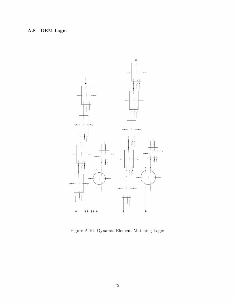
A.8 DEM Logic
vdd gnd
gnd
vdd
vdd
vdd
vdd
vdd
gnd
gnd
gnd
gnd
clk2
clk1
gndvdd
sel
GNDVDD
gndvdd
gndvdd
gndvdd
fine_
out<
30:0
>ou
t<30
:0>
rot_
1_31
_bit
in<3
0:1>
sel_
bar
rot_
31_c
ont<
0>
rot_
31_c
ont_
bar<
0>
out<
30:0
>ro
t_2_
31_b
it
in<3
0:0>
sel
sel_
bar
rot_
31_c
ont<
1>
rot_
31_c
ont_
bar<
1>
out<
30:0
>
in<3
0:0>
sel
sel_
bar
rot_
4_31
_bit
rot_
31_c
ont<
2>
rot_
31_c
ont_
bar<
2>
out<
30:0
>
in<3
0:0>
sel
sel_
bar
rot_
8_31
_bit
rot_
31_c
ont<
3>
rot_
31_c
ont_
bar<
3>
gndvdd
out<
30:0
>
in<3
0:0>
sel
sel_
bar
rot_
16_3
1_bi
tro
t_31
_con
t<4>
rot_
31_c
ont_
bar<
4>
fine_
th<3
0:0>
fine_
bin<
4:0>
rot_
31_c
ont<
4:0>
A<4
:0>
B<4
:0>
adde
r_5b
Ove
rflow
Sum
<4:0
>
vdd
gnd
clk2
gnd
vdd
clk1
clk1
clk2
D<4
:0>
d-re
gist
er_5
b
Q<4
:0>
Q_b
ar<4
:0>
rot_
31_c
ont<
4:0>
rot_
31_c
ont_
bar<
4:0>
coar
se_o
ut<1
5:0>
vdd gndgndvdd
out<
15:0
>ro
t_1_
16_b
it
in<1
5:0>
sel
sel_
bar
rot_
16_c
ont<
0>
rot_
16_c
ont_
bar<
0>
vdd gndgndvdd
out<
15:0
>ro
t_2_
16_b
it
in<1
5:0>
sel
sel_
bar
rot_
16_c
ont<
1>
rot_
16_c
ont_
bar<
1>
vdd gndgndvdd
out<
15:0
>ro
t_4_
16_b
it
in<1
5:0>
sel
sel_
bar
rot_
16_c
ont<
2>
rot_
16_c
ont_
bar<
2>
vdd gndgndvdd
out<
15:0
>ro
t_8_
16_b
it
in<1
5:0>
sel
sel_
bar
rot_
16_c
ont<
3>
rot_
16_c
ont_
bar<
3>
vdd,
coa
rse_
th<1
4:0>
coar
se_t
h<14
:0>
vdd
gnd
coar
se_b
in<3
:0>
vdd gndGNDVDD
rot_
16_c
ont<
3:0>
A<3
:0>
B<3
:0>
adde
r_4b
Ove
rflow
Sum
<3:0
>
vdd
gnd
clk2
gnd
vdd
clk1
clk1
clk2
D<3
:0>
d-re
gist
er_4
b
Q<3
:0>
Q_b
ar<3
:0>
rot_
16_c
ont<
3:0>
rot_
16_c
ont_
bar<
3:0>
Figure A.16: Dynamic Element Matching Logic
72

A.8.1 16-line Rotate-1 Logic
Mux
_2to
1
Mux
_2to
1
in<1
1>
in<1
0>
in<9
>
in<8
>in
<4>
in<5
>
in<6
>
in<7
>in
<3>
in<0
>in
<12>
in<1
3>
in<1
4>
in<1
5>
in<0
>
in<1
>
in<4
>
in<5
>
in<6
>
in<7
>
in<8
>
in<9
>
in<1
0>
in<1
1>
in<1
2>
in<1
4>
in<1
3>
in<1
5>
out<
0>
out<
1>
out<
4>
out<
7>
out<
8>
out<
9>
out<
10>
out<
11>
out<
12>
out<
13>
out<
14>
out<
15>
sel_bar
sel
sel_bar
sel
sel_bar
sel
sel_bar
sel
gnd
vdd
gnd
vdd
gnd
vdd
out<
5>
out<
6>
sel
sel_
bar
out<
15:0
>
in<1
5:0>gnd
vdd
sel_bar
selgnd
vdd
out sel_bar
sel
gnd
vdd
out
sel
Mux
_2to
1
in<2
>
in<3
>
out<
3>
gnd
vdd
sel_bar
selgnd
vdd
out
in0
in1
in<1
>
in<2
>
out<
3>M
ux_2
to1 sel_bar
selgnd
vdd
out
in0
in1
in0
in1 in0
in1
Mux
_2to
1 sel_bar
selgnd
vdd
out
in0
in1
Mux
_2to
1 sel_bar
selgnd
vdd
out
in0
in1
Mux
_2to
1 sel_bar
selgnd
vdd
out
in0
in1
Mux
_2to
1 sel_bar
selgnd
vdd
out
in0
in1
Mux
_2to
1 sel_bar
selgnd
vdd
out
in0
in1
Mux
_2to
1 sel_bar
selgnd
vdd
out
in0
in1
Mux
_2to
1 sel_bar
selgnd
vdd
out
in0
in1
Mux
_2to
1 sel_bar
selgnd
vdd
out
in0
in1
Mux
_2to
1 sel_bar
selgnd
vdd
out
in0
in1
Mux
_2to
1 sel_bar
selgnd
vdd
out
in0
in1
Mux
_2to
1 sel_bar
selgnd
vdd
out
in0
in1
Mux
_2to
1 sel_bar
selgnd
vdd
out
in0
in1
Figure A.17: 16-Input Rotate-1
73
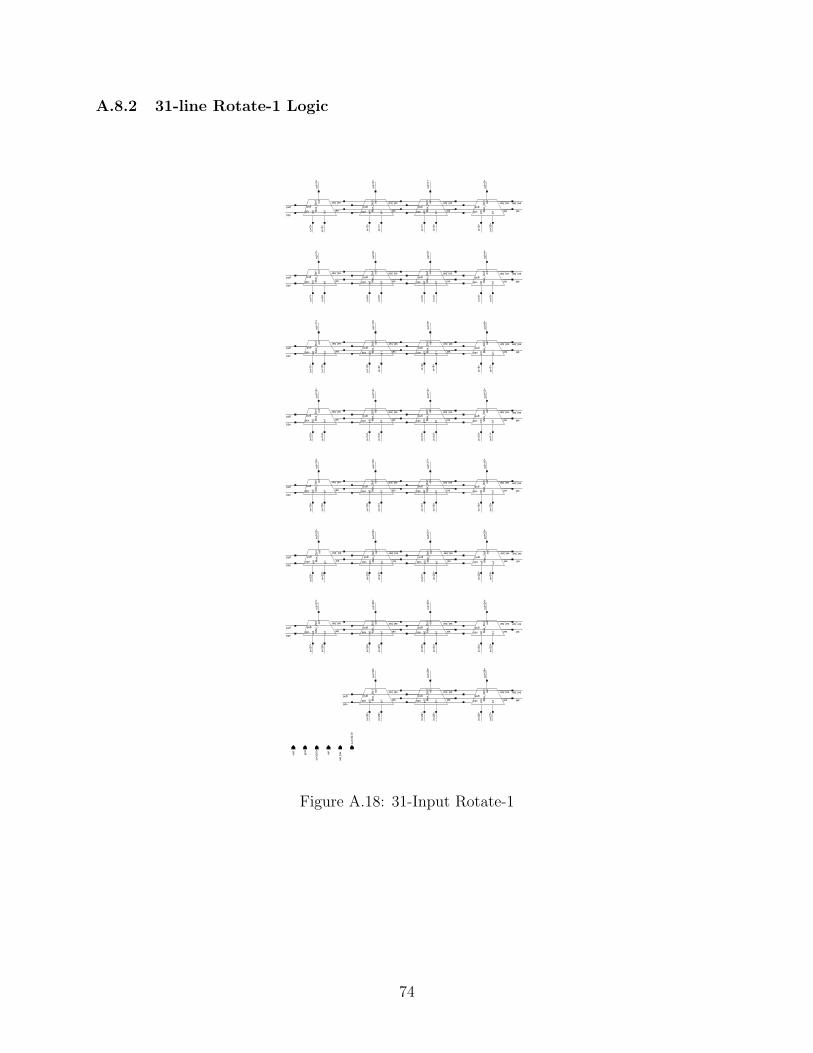
A.8.2 31-line Rotate-1 Logic
in<1
>
in<4
>
in<7
>
in<1
0>
in<0
>
in<5
>
in<6
>
in<1
1>in
<30>
in<2
9>
in<2
8>in
<24>
in<2
5>
in<2
6>
in<2
7>in
<23>
in<2
2>
in<2
1>
in<2
0>in
<16>
in<1
7>
in<1
8>
in<1
9>in
<15>
in<1
4>
in<1
3>
in<1
2>
in<2
>
in<3
>
in<8
>
in<9
>
out<
0>
out<
1>
out<
2>
out<
3>
out<
4>
out<
5>
out<
6>
out<
7>
out<
8>
out<
9>
out<
10>
out<
11>
out<
12>
out<
13>
out<
14>
out<
15>
out<
16>
out<
17>
out<
18>
out<
19>
out<
20>
out<
21>
out<
22>
out<
23>
out<
24>
out<
25>
out<
26>
out<
27>
out<
28>
out<
29>
out<
30>
in<2
6>
sel_bar
sel
sel
sel_bar
sel_bar
sel
sel
sel_bar
vdd
gnd
gnd
vdd
vdd
gnd
gnd
vdd
in<2
1>
in<2
0>
in<1
9>
in<1
8>
in<1
7>
in<1
6>
in<1
5>
in<1
4>
in<1
3>
in<1
2>
in<1
1>
in<1
0>
in<9
>
in<8
>
in<7
>
in<6
>
in<5
>
in<4
>
in<3
>
in<2
>
in<1
>
in<0
>
in<2
5>
in<2
7>
in<2
8>
sel_bar
sel
sel_bar
sel
sel_bar
sel
gnd
vdd
gnd
vdd
gnd
vdd
gnd
vdd
in<3
0>
in<2
9>
in<2
3>
in<2
4>
in<2
2>
sel
sel_
bar
out<
30:0
>
in<3
0:0>
gnd
vdd
Mux
_2to
1 sel_bar
selgnd
vdd
out
in0
in1 M
ux_2
to1 sel_bar
selgnd
vdd
out
in0
in1 M
ux_2
to1 sel_bar
selgnd
vdd
out
in0
in1 M
ux_2
to1 sel_bar
selgnd
vdd
out
in0
in1
Mux
_2to
1 sel_bar
selgnd
vdd
out
in0
in1 M
ux_2
to1 sel_bar
selgnd
vdd
out
in0
in1 M
ux_2
to1 sel_bar
selgnd
vdd
out
in0
in1 M
ux_2
to1 sel_bar
selgnd
vdd
out
in0
in1
Mux
_2to
1 sel_bar
selgnd
vdd
out
in0
in1 M
ux_2
to1 sel_bar
selgnd
vdd
out
in0
in1 M
ux_2
to1 sel_bar
selgnd
vdd
out
in0
in1 M
ux_2
to1 sel_bar
selgnd
vdd
out
in0
in1
Mux
_2to
1 sel_bar
selgnd
vdd
out
in0
in1 M
ux_2
to1 sel_bar
selgnd
vdd
out
in0
in1 M
ux_2
to1 sel_bar
selgnd
vdd
out
in0
in1 M
ux_2
to1 sel_bar
selgnd
vdd
out
in0
in1
Mux
_2to
1 sel_bar
selgnd
vdd
out
in0
in1 M
ux_2
to1 sel_bar
selgnd
vdd
out
in0
in1 M
ux_2
to1 sel_bar
selgnd
vdd
out
in0
in1 M
ux_2
to1 sel_bar
selgnd
vdd
out
in0
in1
Mux
_2to
1 sel_bar
selgnd
vdd
out
in0
in1 M
ux_2
to1 sel_bar
selgnd
vdd
out
in0
in1 M
ux_2
to1 sel_bar
selgnd
vdd
out
in0
in1 M
ux_2
to1 sel_bar
selgnd
vddou
t
in0
in1
Mux
_2to
1 sel_bar
selgnd
vdd
out
in0
in1 M
ux_2
to1 sel_bar
selgnd
vdd
out
in0
in1 M
ux_2
to1 sel_bar
selgnd
vdd
out
in0
in1 M
ux_2
to1 sel_bar
selgnd
vdd
out
in0
in1
Mux
_2to
1 sel_bar
selgnd
vdd
out
in0
in1 M
ux_2
to1 sel_bar
selgnd
vdd
out
in0
in1 M
ux_2
to1 sel_bar
selgnd
vdd
out
in0
in1
sel_bar
sel
Figure A.18: 31-Input Rotate-1
74
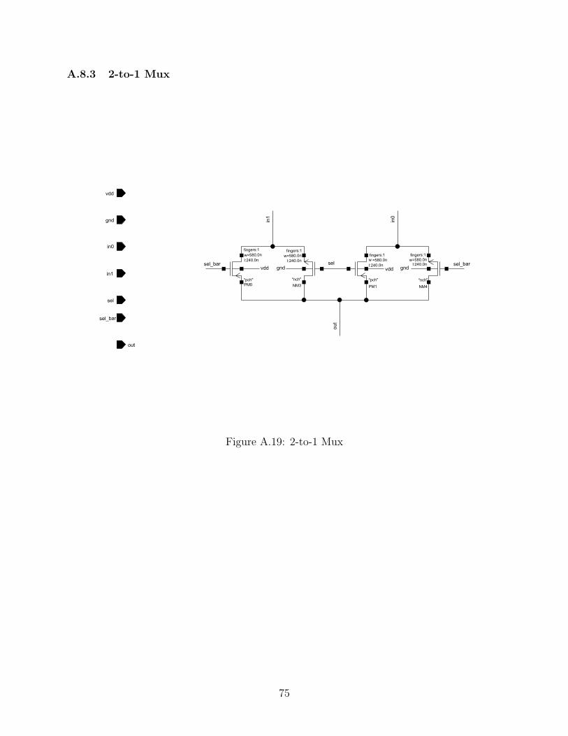
A.8.3 2-to-1 Mux
l:240.0nw=580.0n
"nch"
fingers:1
l:240.0nw=580.0n
"nch"
fingers:1
"pch"
w =580.0nl:240.0n
fingers:1
"pch"
w=580.0nl:240.0n
fingers:1
NM3 NM4PM1PM0
out
in1
in0
sel_bar selvdd gndgndvdd
sel_bar
out
sel_bar
sel
in1
in0
gnd
vdd
Figure A.19: 2-to-1 Mux
75
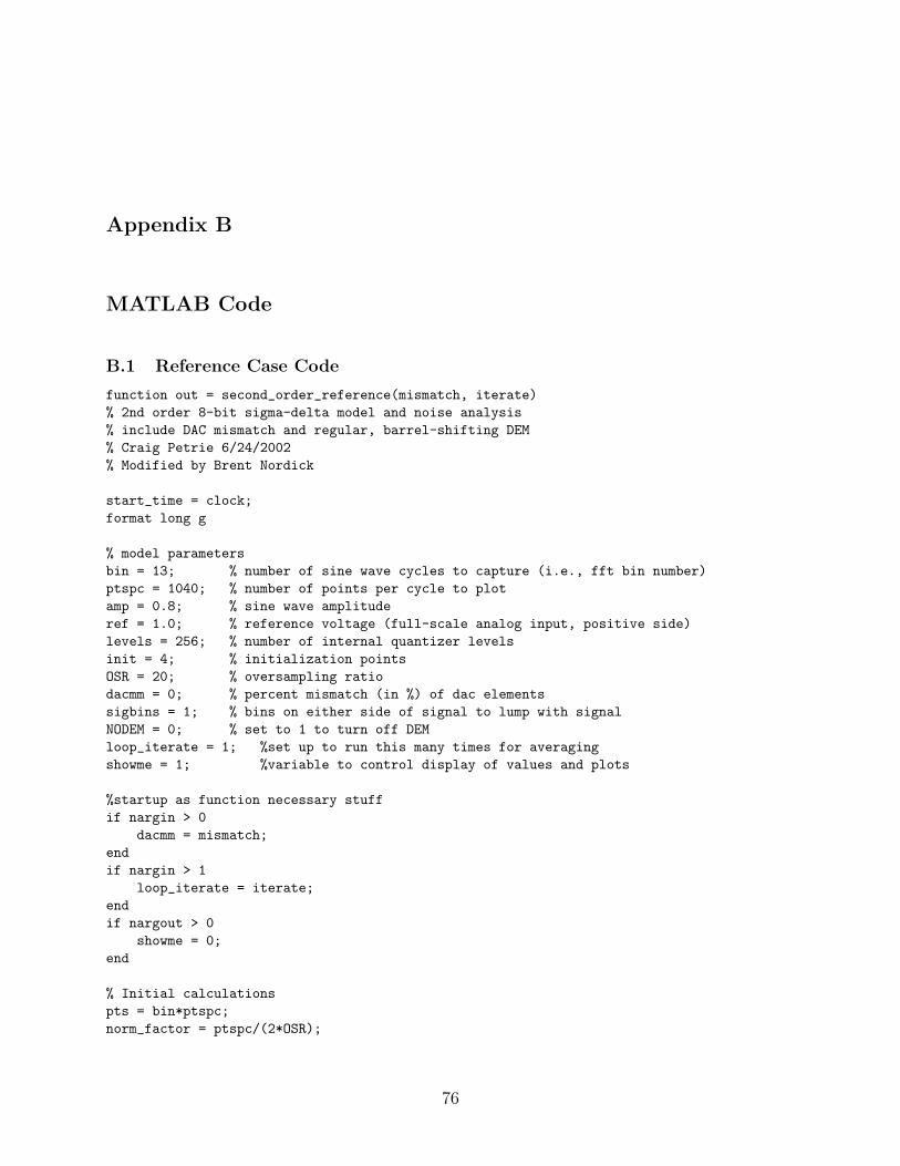
Appendix B
MATLAB Code
B.1 Reference Case Code
function out = second_order_reference(mismatch, iterate)% 2nd order 8-bit sigma-delta model and noise analysis% include DAC mismatch and regular, barrel-shifting DEM% Craig Petrie 6/24/2002% Modified by Brent Nordick
start_time = clock;format long g
% model parametersbin = 13; % number of sine wave cycles to capture (i.e., fft bin number)ptspc = 1040; % number of points per cycle to plotamp = 0.8; % sine wave amplituderef = 1.0; % reference voltage (full-scale analog input, positive side)levels = 256; % number of internal quantizer levelsinit = 4; % initialization pointsOSR = 20; % oversampling ratiodacmm = 0; % percent mismatch (in %) of dac elementssigbins = 1; % bins on either side of signal to lump with signalNODEM = 0; % set to 1 to turn off DEMloop_iterate = 1; %set up to run this many times for averagingshowme = 1; %variable to control display of values and plots
%startup as function necessary stuffif nargin > 0
dacmm = mismatch;endif nargin > 1
loop_iterate = iterate;endif nargout > 0
showme = 0;end
% Initial calculationspts = bin*ptspc;norm_factor = ptspc/(2*OSR);
76

% calculate parameters for internal adc functionlm1 = levels - 1;m = lm1/2/ref; % slopeb = lm1/2; % offset
%set up loop for averaging purposesfor lop = 1:loop_iterate
x = amp*sin(2*pi*bin*[0:pts-1+init]/pts); % exactly ’bin’ cycles of% ’pts’-point sine wave x=A*sin(2*pi*w*t)
%x = -1*ones(1,length(x)); %DC input for testing purposeselm1 = getdac(levels,ref,dacmm); % retrieve dac element values for dac #1elm2 = getdac(levels,ref,0); % retrieve dac element values for dac #2
% main delta-sigma loopu = 0; v = 0; % initialize integrator outputsdemptr = 0; % initialize DEM pointery = zeros(1,pts+init); % allocate and initialize output vectoroneelm = zeros(1,pts+init); % examine frequency content of a single
% element signalfor i = 1:pts+init
[z,y(i)] = idealq(v,m,b,lm1); % quantize using second% integrator output before 2nd% integration
if (NODEM)demptr = 0;
end % remove DEM pointer memory to turn off DEM[dacvec,demptr] = dem(z,lm1,demptr); % call DEM (Dynamic Element
% Matching) algorithmoneelm(i) = dacvec(1); % look at first elementv = v + 2*(u - sum(dacvec.*elm2)); % 2nd integration, use 1st
% integrator output before 1st integrationu = u + 0.5*(x(i) - sum(dacvec.*elm1)); % 1st integration
end
% plot waveforms, spectrumx = x(init+1:pts+init); % grab last part of data - ignore init portiony = y(init+1:pts+init); % grab last part of data - ignore init portionptsv = 1:pts;yspec = mypsd(y);
% calculate snrsigtonoise = mysnr(yspec,bin,OSR);sig_to_noise(lop) = sigtonoise; %vector of values to average
% compare with ideal snr of 2nd-order modulatorsigi = amp/sqrt(2); % rms voltage of sine wavenoisei = 2*ref/levels/sqrt(12)*(pi)^2/sqrt(5)/(OSR)^2.5;
% theoretical rms quantization noise voltagesigtonoisei = 20*log10(sigi/noisei);
% calculate sfdrsigv = yspec(max([1,(bin-sigbins)]):bin+sigbins); % signal plus spectral bleednoisev = [yspec(1:bin-sigbins-1) yspec(bin+sigbins+1:pts/2/OSR)]; % vector of
% bins used to calculate noise
77
sfdr = 10*log10(max(sigv)/max(noisev));avg_sfdr(lop) = sfdr;
end
%calculate values for loopingif (loop_iterate ~= 1)
sig_to_noise = sort(sig_to_noise);out_sig_to_noise(1) = sig_to_noise(1);out_sig_to_noise(2) = mean(sig_to_noise);out_sig_to_noise(3) = sig_to_noise(loop_iterate);
avg_sfdr = sort(avg_sfdr);out_sfdr(1) = avg_sfdr(1);out_sfdr(2) = mean(avg_sfdr);out_sfdr(3) = avg_sfdr(loop_iterate);
elseout_sig_to_noise = sigtonoise;out_sfdr = sfdr;
end
if (showme)%Plotfigure(2);
%subplot(2,2,1);plot(ptsv,x,ptsv,y);title(’Time domain waves - sampled and quantized’);legend(’sampled wave’,’quantized wave’);xlabel(’time’);ylabel(’voltage’);
figure(3);subplot(2,1,1);
semilogx(10*log10(yspec));title(’Power Spectrum’);xlabel(’Frequency’);ylabel(’Power’);
% look at spectra of single elementsoneelm = oneelm(init+1:pts+init);subplot(2,1,2);
ospec = mypsd(oneelm);semilogx(10*log10(ospec));title(’Single Element Power Spectrum’);xlabel(’Frequency’);ylabel(’Power’);
figure(1);%subplot(2,1,1)
semilogx(10*log10(yspec));title(’Power Spectrum’);xlabel(’Frequency’);ylabel(’Power’);
78

% display avg/max/min on looping, or just the output when notsigtonoiseiout_sig_to_noiseout_sfdr
else%output of the functionout = out_sig_to_noise;
end
elapsed_time = etime(clock, start_time)
function elmvec = getdac(levs,fs,mm)% calculate random element values for the dac; each element either added or% subtracted
% levs output levels generated by the dac; there are (levs-1) elements% fs full scale output value, positive side% mm desired dac element mismatch, in percent% elmvec output vector containing (levs-1) dac element valuesnom = fs/(levs-1); % ideal dac element value (mean
% of output array)elmvec = nom*(1 + 0.01*mm*randn(1,levs-1)); % 1-by-(levs-1) array of random
% element values
function [intout,dubout] = idealq(in,m,b,maxin)% ideal quantization using pre-calculate slope and intercept values% in value to be quantized% m input multiplier before rounding% b input offset before rounding% maxin output code forced to be in range [0,maxin]% codout output integer quantized value% dubout output double quantized value (with same input range as ’in’)intout = round(m*in + b);intout = max([intout,0]);intout = min([intout,maxin]);dubout = (intout - b)/m;
function [vecout,ptrout] = dem(code,lm1,ptrin)% perform barrel-shifing dem algorithm% code input integer code% lm1 (# dac output levels) - 1; number of dac elements% ptrin position where elements start getting used this time, in range% [0,levs-1]
% vecout boolean output vector (+1 or -1) corresp to ’on’ elements in the DAC% ptrout position where elements start getting used next time, in range% [0,levs-1]
ptrout = mod(ptrin+code,lm1);if ((ptrout > ptrin) | (code == 0))
vecout = [repmat(-1,1,ptrin),repmat(1,1,code),repmat(-1,1,lm1-code-ptrin)];else % (ptrout < ptrin) | (code == lm1)
vecout =[repmat(1,1,code+ptrin-lm1),repmat(-1,1,lm1-code),repmat(1,1,lm1-ptrin)];
end
79
B.2 Calibration Code
function out = second_order_calibrate(mm_fine, iterate)% 2nd order sigma-delta model and noise analysis% include DAC mismatch and course/fine DEM% Craig Petrie 6/24/2002% Brent Nordick 12-10-03
start_time = clock;format long g
% model parametersbin = 13; % number of sine wave cycles to capture (i.e., fft bin number)ptspc = 1040; % number of points per cycleamp = 0.8; % sine wave amplituderef = 1.0; % reference voltage (full-scale analog input, positive side)clevs = 16; % number of course levels (output codes) in two-step internal
% quantizerflevs = 16; % number of fine levels in internal quantizerinit = 4; % initialization pointsOSR = 20; % oversampling ratiodacmmc = 0; % percent mismatch (in %) of course dac elementsdacmmf = 0; % percent mismatch (in %) of fine dac elementssigbins = 1; % bins on either side of signal to lump with signalNODEM = 0; % set to 1 to turn off DEMloop_iterate = 1; %Make it loop to get average StoNshowme = 1; %variale to control display of values and plots
%startup as function necessary stuffif nargin > 0
dacmmf = mm_fine;endif nargin > 1
loop_iterate = iterate;endif nargout > 0
showme = 0;end
% Initial calculationspts = bin*ptspc;norm_factor = ptspc/(2*OSR);
% calculate parameters for internal two-step adc function% for fine quantization, input signal is in the range [-ref/clevs,+ref/clevs]olevs = clevs*flevs; % number of overall levels in internal quantizerolm1 = olevs - 1;clm1 = clevs - 1;flm1 = flevs - 1;mc = olm1/2/flevs/ref; % slope for course quantizationbc = clm1/2; % offset for course quantizationmf = olm1/2/ref; % slope for fine quantizationbf = flm1/2; % offset for fine quantization
80

%set up loop for averaging purposesfor lop = 1:loop_iterate
x = amp*sin(2*pi*bin*[0:pts-1+init]/pts); % exactly ’bin’ cycles of% ’pts’-point sine wave
[elm1c,elm1f] = getdac2(clevs,flevs,ref,dacmmc,dacmmf); % retrieve dac% element values for dac #1
[elm2c,elm2f] = getdac2(clevs,flevs,ref,0,0); % retrieve dac% element values for dac #2
%compute averages and adjust fine values so that the average is the same%this translates to same average gain
avgc = sum(elm1c)/size(elm1c,2);avgf = sum(elm1f)/size(elm1f,2);deltaf = (avgc/16-avgf);deltac = (avgf*16-avgc);avg_cap_calculated = [avgc avgf];%save for analysisdelta_list(lop)=deltaf;avgc_list(lop) = avgc;avgf_list(lop) = avgf;
% main delta-sigma loopu = 0; v = 0; % initialize integrator outputsdemptrc = 0; demptrf = 0; % initialize DEM pointersy = zeros(1,pts+init); % allocate and initialize output vectormydisp = 1;corselm = zeros(1,pts+init); % examine frequency content of a single
% course element signalfineelm = zeros(1,pts+init); % examine frequency content of a single fine
% element signalyc = zeros(1,pts+init); % examine course adc output signalyf = zeros(1,pts+init); % examine fine adc output signal
%cal length and M for third order sync% 868 289% 2170 723% 4123 1374% 8680 2893%16492 5497
%Calibration routinefigure(2);subplot(2,1,1);cal_length = 16492;for lop1 = 1:2
for lop2 = 1:cal_length%[zc,zf,y(lop2),yc(lop2),yf(lop2)] =
idealq2(v,mc,bc,mf,bf,clm1,flm1); % two-step quantization; use% second integrator output 1st
if (lop1 == 1)zc = 1;zf = 1;
end
81

if (lop1 == 2);zc = 1;zf = 1;
endzcal(lop2) = idealq_1b(v);if (lop1 ==1)
[dacvecc,demptrc] = dem(zc,clm1,demptrc);v = v + 2*(u - sum(dacvecc.*elm2c) - zcal(lop2));
% 2nd integrationu = u + 0.5*(0 - sum(dacvecc.*elm1c) - zcal(lop2));
% 1st integrationelse
[dacvecf,demptrf] = dem(zf,flm1,demptrf);v = v + 2*(u - sum(dacvecf.*elm2f) - zcal(lop2));
% 2nd integrationu = u + 0.5*(0 - sum(dacvecf.*elm1f) - zcal(lop2));
% 1st integrationend
endplot([1:cal_length],zcal)axis([0,cal_length,-1.1,1.1]);output_cal(lop1,:) = zcal(1:cal_length);title(’Coarse Calibration Routine’);subplot(2,1,2);
endtitle(’Fine Calibration Routine’);
%Calibration valuesM = 5497;b = [1 zeros(1,M-1) -3 zeros(1,M-1) 3 zeros(1,M-1) -1];
% 3rd order sinc filtera = (M^3)*[1 -3 3 -1];yprime(1,:) = filter(b, a, output_cal(1,:));yprime(2,:) = filter(b, a, output_cal(2,:));figure(3)
plot(yprime(1,:))hold onplot(yprime(2,:),’r’)hold offlegend(’coarse’,’fine’)
avg_y(1) = yprime(1,cal_length);avg_y(2) = yprime(2,cal_length);%avg_filtered = avg_y
%remove ; for displayingavg_cap = ((avg_y ./ 13)) *[[1/1 0]; [0 1/1]];error(lop,:) = avg_cap - avg_cap_calculated;delta_cap =[ (avg_cap(2)*flevs - avg_cap(1)) (avg_cap(1)/(flevs) -avg_cap(2))];
%elm1c(1) = elm1c(1) + (clevs-1)*delta_cap(1);elm1f(1) = elm1f(1) + (flevs-1)*delta_cap(2);%elm1c = elm1c + delta_cap(1);%elm1f = elm1f + delta_cap(2);
82

%Standard operationu = 0; v = 0; % initialize integrator outputsdemptrc = 0; demptrf = 0; % initialize DEM pointersy = zeros(1,pts+init); % allocate and initialize output vectorfor i = 1:pts+init
[zc,zf,y(i),yc(i),yf(i)] = idealq2(v,mc,bc,mf,bf,clm1,flm1); % two-step% quantization; use second integrator output 1st
if (NODEM) % remove DEM pointer memory to turn off DEMdemptrc = 0; demptrf = 0;
end[dacvecc,demptrc] = dem(zc,clm1,demptrc); % call DEM (Dynamic
% Element Matching) algorithm for course dac[dacvecf,demptrf] = dem(zf,flm1,demptrf); % call DEM (Dynamic
% Element Matching) algorithm for fine daccorselm(i) = dacvecc(1); % look at first elementfineelm(i) = dacvecf(1); % look at first elementv = v + 2*(u - sum(dacvecc.*elm2c) - sum(dacvecf.*elm2f));
% 2nd integrationu = u + 0.5*(x(i) - sum(dacvecc.*elm1c) - sum(dacvecf.*elm1f));
% 1st integrationend
% plot waveforms, spectrumx = x(init+1:pts+init); % grab last part of datay = y(init+1:pts+init); % grab last part of dataptsv = 1:pts;yspec = mypsd(y);
% calculate snrsigv = yspec(max([1,(bin-sigbins)]):bin+sigbins);
% signal plus spectral bleednoisev = [yspec(1:bin-sigbins-1) yspec(bin+sigbins+1:pts/2/OSR)];
% vector of bins used to calculate noisesig = sum(sigv); noise = sum(noisev);sigtonoise = 10*log10(sig/noise);sig_to_noise(lop) = sigtonoise; %vector of values to average
% compare with ideal snr of 2nd-order modulatorsigi = amp/sqrt(2); % rms voltage of sine wavenoisei = 2*ref/clevs/flevs/sqrt(12)*(pi)^2/sqrt(5)/(OSR)^2.5;
% theoretical rms quantization noise voltagesigtonoisei = 20*log10(sigi/noisei);
% calculate sfdrsfdr = 10*log10(max(sigv)/max(noisev));avg_sfdr(lop) = sfdr;
end
%calculate values for loopingif (loop_iterate ~= 1)
83

sig_to_noise = sort(sig_to_noise);out_sig_to_noise(1) = sig_to_noise(1);out_sig_to_noise(2) = mean(sig_to_noise);out_sig_to_noise(3) = sig_to_noise(loop_iterate);
avg_sfdr = sort(avg_sfdr);out_sfdr(1) = avg_sfdr(1);out_sfdr(2) = mean(avg_sfdr);out_sfdr(3) = avg_sfdr(loop_iterate);
%delta resultsavgc_list = sort(avgc_list);out_avgc(1) = avgc_list(1);out_avgc(2) = mean(avgc_list);out_avgc(3) = avgc_list(loop_iterate);
avgf_list = sort(avgf_list);out_avgf(1) = avgf_list(1);out_avgf(2) = mean(avgf_list);out_avgf(3) = avgf_list(loop_iterate);
delta_list = sort(abs(delta_list));out_delta(1) = delta_list(1);out_delta(2) = mean(delta_list);out_delta(3) = delta_list(loop_iterate);
out = out_sig_to_noise;else
out_sig_to_noise = sigtonoise;out_sfdr = sfdr;%delta resultsout_avgc = avgc;out_avgf = avgf;out_delta = deltaf;
end
if (showme)%Plotsfigure(22);plot(ptsv,x,ptsv,y);title(’Time domain waves - sampled and quantized’);legend(’sampled wave’,’ideal quantized wave’);xlabel(’time’);ylabel(’voltage’);
figure(1);%subplot(2,1,2);
semilogx(10*log10(yspec)); % plot ittitle(’Power Spectrum of output signal (using FFT) (y) - Dual DEM withGain Equalization’);
xlabel(’Frequency’);ylabel(’Power’);axis([10^0 10^4 -150 100])
84
% look at spectra of course and fine elements and signalscorselm = corselm(init+1:pts+init);fineelm = fineelm(init+1:pts+init);yc = yc(init+1:pts+init);yf = yf(init+1:pts+init);
figure(23);subplot(2,2,1);
cspec = (abs(fft(corselm))).^2; % power spectrum using fftcspec = cspec(2:pts/2+1); % only interested one side, forget dcsemilogx(10*log10(cspec)); % plot ittitle(’Single Element Course Power Spectra (corselm)’);xlabel(’Frequency’);ylabel(’Power’);
subplot(2,2,3);fspec = (abs(fft(fineelm))).^2; % power spectrum using fftfspec = fspec(2:pts/2+1); % only interested one side, forget dcsemilogx(10*log10(fspec)); % plot ittitle(’Single Element Fine Power Spectra (fineelm)’);xlabel(’Frequency’);ylabel(’Power’);
subplot(2,2,2);cspec = (abs(fft(yc))).^2; % power spectrum using fftcspec = cspec(2:pts/2+1); % only interested one side, forget dcsemilogx(10*log10(cspec)); % plot ittitle(’Course Output Power Spectra (yc)’);xlabel(’Frequency’);ylabel(’Power’);
subplot(2,2,4);fspec = (abs(fft(yf))).^2; % power spectrum using fftfspec = fspec(2:pts/2+1); % only interested one side, forget dcsemilogx(10*log10(fspec)); % plot ittitle(’Fine Output Power Spectra (yf)’);xlabel(’Frequency’);ylabel(’Power’);
% display avg/max/min on looping, or just the output when notnorm_factorsigtonoiseiout_sig_to_noiseout_sfdrout_avgcout_avgfout_delta
else%output of the functionout = out_sig_to_noise;
end
elapsed_time = etime(clock, start_time)
function [out] = idealq_1b(in)
85

%ideal 1 bit quantization for calibrate routine% in value to be quantized% Simple comparatorif (in > 0)
out = 1;else
out = -1;end
function [elmc,elmf] = getdac2(clevs,flevs,fs,mmc,mmf)% calculate random element values course and fine dac arrays; each element
% either added or subtracted% clevs course output levels generated by the dac; there are (clevs-1)
% course elements% flevs fine output levels generated by the dac; there are (flevs-1) fine
% elements% fs full scale output value, positive side% mmc desired course dac element mismatch, in percent% mmf desired fine dac element mismatch, in percent% elmc output vector containing (clevs-1) course dac element values% elmf output vector containing (flevs-1) fine dac element values%randn(’state’,sum(100*clock)); %randomly reset random number seednomc = fs*flevs/(clevs*flevs - 1); % ideal course dac element value
% (mean of output array)nomf = fs/(clevs*flevs - 1); % ideal fine dac element value
% (mean of output array)%elmc = nomc*(1 + 0.01*mmc*randn(1,clevs-1)); % 1-by-(clevs-1) array of
% random element valueselmf = nomf*(1 + 0.01*mmf*randn(1,flevs-1)); % 1-by-(clevs-1) array of
% random element valuesfor lop = 1:clevs-1
elmc(lop) = sum(nomf*(1 + 0.01*mmf*randn(1,flevs)));end%stdev_f = std(elmf)/nomf%stdev_c = std(elmc)/nomc%calc_stdv = sqrt(sum((elmc-nomc).^2)/16) / nomc
function [outc,outf,dubout,dubc,dubf] = idealq2(in,mc,bc,mf,bf,maxc,maxf)% ideal 2-step (course,fine) quantization using pre-calculated slope and
% intercept values% in value to be quantized% mc course input multiplier before rounding% mf fine input multiplier before rounding% bc course input offset before rounding% bf fine input offset before rounding% maxc course output code is forced to be in range [0,maxc]% maxf fine output code is forced to be in range [0,maxf]% outc course output integer quantized value% outf fine output integer quantized value% dubout output double quantized value (with same input range as ’in’)% dubc course quantized value (with same input range as ’in’)% dubf fine quantized value (with same input range as ’in’, but scaled
% to be fine)outc = round(mc*in + bc); % 1st (course) quantization step
86

outc = max([outc,0]);outc = min([outc,maxc]);dubc = (outc - bc)/mc;outf = round(mf*(in - dubc) + bf); % 2nd (fine) quantization stepoutf = max([outf,0]);outf = min([outf,maxf]);dubf = (outf - bf)/mf;dubout = dubc + dubf;
function [vecout,ptrout] = dem(code,lm1,ptrin)% perform barrel-shifing dem algorithm% code input integer code% lm1 (# dac output levels) - 1; number of dac elements% ptrin position where elements start getting used this time, in range
% [0,levs-1]% vecout boolean output vector (+1 or -1) corresp to ’on’ elements in the
% DAC% ptrout position where elements start getting used next time, in range
% [0,levs-1]ptrout = mod(ptrin+code,lm1);if ((ptrout > ptrin) | (code == 0))
vecout =[repmat(-1,1,ptrin),repmat(1,1,code),repmat(-1,1,lm1-code-ptrin)];
else % (ptrout < ptrin) | (code == lm1)vecout =[repmat(1,1,code+ptrin-lm1),repmat(-1,1,lm1-code),repmat(1,1,lm1-ptrin)];
end
87

B.3 ReQ Code
function out = second_order_ReQ(mm_caps, iterate)% 2nd order 8-bit sigma-delta model and noise analysis% include DAC mismatch and coarse/fine DEM% Craig Petrie 6/24/2002% Modified by Brent Nordick
start_time = clock;format long g
% model parametersbin = 13; % number of sine wave cycles to capture (i.e., fft bin number)ptspc = 1040; % number of points per cycleamp = 0.8; % sine wave amplituderef = 1.0; % reference voltage (full-scale analog input, positive side)clevs = 16; % number of coarse levels (output codes) in two-step internal
% quantizerflevs = 16; % number of fine levels in internal quantizerclevs_ReQ = 16; % number of coarse levels (output codes) in ReQ circuitry -
% flevs_ReQ is automatically calculated%flevs_ReQ = 32; % number of fine levels in ReQ circuitry (total of the ReQ bits
% should be 1 extra for the overlap)init = 4; % initialization pointsOSR = 20; % oversampling ratiodacmmc = 0; % percent mismatch (in %) of coarse dac elementsdacmmf = 0; % percent mismatch (in %) of fine dac elementssigbins = 1; % bins on either side of signal to lump with signalNODEM = 0; % set to 1 to turn off DEMloop_iterate = 1; %Make it loop to get average StoNshowme = 1; %variable to control display of values and plots
%startup as function necessary stuffif nargin > 0
dacmmf = mm_caps;endif nargin > 1
loop_iterate = iterate;endif nargout > 0
showme = 0;end
% Initial calculationspts = bin*ptspc;norm_factor = ptspc/(2*OSR);flevs_ReQ = 2*clevs*flevs/clevs_ReQ;
% calculate parameters for internal two-step adc function% for fine quantization, input signal is in the range [-ref/clevs,+ref/clevs]olevs = clevs*flevs; % number of overall levels in internal quantizerolm1 = olevs - 1;clm1 = clevs - 1;flm1 = flevs - 1;
88

mc = olm1/2/flevs/ref; % slope for coarse quantizationbc = clm1/2; % offset for coarse quantizationmf = olm1/2/ref; % slope for fine quantizationbf = flm1/2; % offset for fine quantization
%set up loop for averaging purposesfor lop = 1:loop_iterate
x = amp*sin(2*pi*bin*[0:pts-1+init]/pts); % exactly ’bin’ cycles of% ’pts’-point sine wave
[elm1c,elm1f] = getdac2(clevs,flevs,clevs_ReQ,flevs_ReQ,ref,dacmmc,dacmmf);% retrieve dac element values for dac #1
[elm2c,elm2f] = getdac2(clevs,flevs,clevs_ReQ,flevs_ReQ,ref,0,0);% retrieve dac element values for dac #2
% main delta-sigma loopu = 0; v = 0; % initialize integrator outputsdemptrc = 0; demptrf = 0; % initialize DEM pointersy = zeros(1,pts+init); % allocate and initialize output vectormydisp = 1;corselm = zeros(1,pts+init); % examine frequency content of a single
% coarse element signalfineelm = zeros(1,pts+init); % examine frequency content of a single fine
% element signalyc = zeros(1,pts+init); % examine coarse adc output signalyf = zeros(1,pts+init); % examine fine adc output signalzerr = 0;dub_err = 0;maxf = 0;minf = 0;for i = 1:pts+init
[zc,zf,y(i),yc(i),yf(i)] = idealq2(v,mc,bc,mf,bf,clm1,flm1); % two-step% quantization; use second integrator output 1st
if (NODEM) % remove DEM pointer memory to turn off DEMdemptrc = 0; demptrf = 0;
end
%noise shape gain error between DAC’sdub_mod = y(i)-dub_err;
%dub_mod(i)=min([max([dub_mod(i),-1]),1]);%limit to allowable range
z_mod_8_b = min([max([round((olm1)/2*(dub_mod) + (olm1)/2),0]),olm1]);z_mod_4_b = floor(z_mod_8_b/(flevs_ReQ/2));
zc = z_mod_4_b;zc = max([zc 0]);zc = min([zc 15]);
z_mod_4_b_ls = z_mod_4_b * (flevs_ReQ/2);dub_4_b_ls = (z_mod_4_b_ls - ((olm1)/2))/((olm1)/2);
dub_err = dub_4_b_ls-dub_mod;%dub_err=min([max([dub_err,-1]),1]); %limit to allowable range
dub_fine = y(i) - dub_4_b_ls;z_fine_8b = min([max([round((olm1)/2*dub_fine+(olm1)/2),0]),olm1]);
89

zf = z_fine_8b-(olevs-flevs_ReQ)/2;%this converts from 8 bit to 5 bit bias number
zf = max([zf 0]);zf = min([zf 31]);
yc(i) = (zc * (flevs_ReQ/2) - ((olm1)/2))/((olm1)/2);yf(i) = (zf + (olevs-flevs_ReQ)/2 - ((olm1)/2))/((olm1)/2);
%end noise shape stuff
[dacvecc,demptrc] = dem(zc,clevs_ReQ-1+1,demptrc); % call DEM (Dynamic% Element Matching) algorithm for coarse dac
[dacvecf,demptrf] = dem(zf,flevs_ReQ-1,demptrf); % call DEM (Dynamic% Element Matching) algorithm for fine dac
corselm(i) = dacvecc(1); % look at first elementfineelm(i) = dacvecf(1); % look at first elementv = v + 2*(u - sum(dacvecc.*elm2c) - sum(dacvecf.*elm2f) );
% 2nd integrationu = u + 0.5*(x(i) - sum(dacvecc.*elm1c) - sum(dacvecf.*elm1f) );
% 1st integrationend
% plot waveforms, spectrumx = x(init+1:pts+init); % grab last part of datay = y(init+1:pts+init); % grab last part of dataptsv = 1:pts;yspec = mypsd(y);
% calculate snrsigv = yspec(max([1,(bin-sigbins)]):bin+sigbins); % signal plus spectral bleednoisev = [yspec(1:bin-sigbins-1) yspec(bin+sigbins+1:pts/2/OSR)];
% vector of bins used to calculate noisesig = sum(sigv);noise = sum(noisev);sigtonoise = 10*log10(sig/noise);sig_to_noise(lop) = sigtonoise; %vector of values to average
% compare with ideal snr of 2nd-order modulatorsigi = amp/sqrt(2); % rms voltage of sine wavenoisei = 2*ref/clevs/flevs/sqrt(12)*(pi)^2/sqrt(5)/(OSR)^2.5;
% theoretical rms quantization noise voltagesigtonoisei = 20*log10(sigi/noisei);
% calculate sfdrsfdr = 10*log10(max(sigv)/max(noisev));avg_sfdr(lop) = sfdr;
end
%calculate values for loopingif (loop_iterate ~= 1)
sig_to_noise = sort(sig_to_noise);out_sig_to_noise(1) = sig_to_noise(1);out_sig_to_noise(2) = mean(sig_to_noise);out_sig_to_noise(3) = sig_to_noise(loop_iterate);
90
avg_sfdr = sort(avg_sfdr);out_sfdr(1) = avg_sfdr(1);out_sfdr(2) = mean(avg_sfdr);out_sfdr(3) = avg_sfdr(loop_iterate);
elseout_sig_to_noise = sigtonoise;out_sfdr = sfdr;
end
%Outputif (showme)
% Plotsfigure(22);plot(ptsv,x,ptsv,y);title(’Time domain waves - sampled and quantized’);legend(’sampled wave’,’ideal quantized wave’);xlabel(’time’);ylabel(’voltage’);
figure(1);%subplot(2,1,2);
semilogx(10*log10(yspec)); % plot ittitle(’Power Spectrum (using FFT) (y) - Dual DEM with segmented noiseshaping’);
xlabel(’Frequency’);ylabel(’Power’);axis([10^0 10^4 -150 100])
% look at spectra of coarse and fine elements and signalscorselm = corselm(init+1:pts+init);fineelm = fineelm(init+1:pts+init);yc = yc(init+1:pts+init);yf = yf(init+1:pts+init);
figure(23);subplot(2,2,1);
cspec = mypsd(corselm);semilogx(10*log10(cspec)); % plot ittitle(’Single Element Coarse Power Spectra (corselm)’);xlabel(’Frequency’);ylabel(’Power’);
subplot(2,2,3);fspec = mypsd(fineelm);semilogx(10*log10(fspec)); % plot ittitle(’Single Element Fine Power Spectra (fineelm)’);xlabel(’Frequency’);ylabel(’Power’);
subplot(2,2,2);cspec = mypsd(yc);semilogx(10*log10(cspec)); % plot ittitle(’Coarse Output Power Spectra (yc)’);
91

xlabel(’Frequency’);ylabel(’Power’);
subplot(2,2,4);fspec = mypsd(fspec);semilogx(10*log10(fspec)); % plot ittitle(’Fine Output Power Spectra (yf)’);xlabel(’Frequency’);ylabel(’Power’);
% display avg/max/min on looping, or just the output when notnorm_factorsigtonoiseiout_sig_to_noiseout_sfdr
else%output of the functionout = out_sig_to_noise;
end
time_elapsed = etime(clock, start_time)
function [elmc,elmf] = getdac2(clevs,flevs,clevs_ReQ,flevs_ReQ,fs,mmc,mmf)% calculate random element values coarse and fine dac arrays; each element
% either added or subtracted% clevs coarse output levels generated by the dac;% flevs fine output levels generated by the dac;% clevs_ReQ Coarse output levels from the ReQ circuitry; there are
% (clevs_ReQ-1) coarse elements (plus one for offset)% flevs_ReQ Fine output levels from the ReQ circuitry; there are
% (flevs_ReQ-1) fine elements% fs full scale output value, positive side% mmc desired coarse dac element mismatch, in percent% mmf desired fine dac element mismatch, in percent% elmc output vector containing (clevs-1) coarse dac element values% elmf output vector containing (flevs-1) fine dac element values%randn(’state’,sum(100*clock)); %randomly reset random number seednomc = fs*(flevs_ReQ/2)/(clevs*flevs - 1); % ideal coarse dac element value
% (mean of output array)nomf = fs/(clevs*flevs - 1); % ideal fine dac element value
% (mean of output array)%elmc = nomc*(1 + 0.01*mmc*randn(1,clevs_ReQ-1+1)); % 1-by-(clevs-1) array
% of random element valueselmf = nomf*(1 + 0.01*mmf*randn(1,flevs_ReQ-1)); % 1-by-(clevs-1) array of
% random element valuesfor lop = 1:clevs_ReQ-1+1
elmc(lop) = sum(nomf*(1 + 0.01*mmf*randn(1,flevs_ReQ/2)));end%stdev_f = std(elmf)/nomf%stdev_c = std(elmc)/nomc%calc_stdv = sqrt(sum((elmc-nomc).^2)/16) / nomc
function [outc,outf,dubout,dubc,dubf] = idealq2(in,mc,bc,mf,bf,maxc,maxf)% ideal 2-step (coarse,fine) quantization using pre-calculated slope and
% intercept values
92

% in value to be quantized% mc coarse input multiplier before rounding% mf fine input multiplier before rounding% bc coarse input offset before rounding% bf fine input offset before rounding% maxc coarse output code is forced to be in range [0,maxc]% maxf fine output code is forced to be in range [0,maxf]% outc coarse output integer quantized value% outf fine output integer quantized value% dubout output double quantized value (with same input range as ’in’)% dubc coarse quantized value (with same input range as ’in’)% dubf fine quantized value (with same input range as ’in’, but scaled
% to be fine)outc = round(mc*in + bc); % 1st (coarse) quantization stepoutc = max([outc,0]);outc = min([outc,maxc]);dubc = (outc - bc)/mc;outf = round(mf*(in - dubc) + bf); % 2nd (fine) quantization stepoutf = max([outf,0]);outf = min([outf,maxf]);dubf = (outf - bf)/mf;dubout = dubc + dubf;
function [vecout,ptrout] = dem(code,lm1,ptrin)% perform barrel-shifing dem algorithm% code input integer code% lm1 (# dac output levels) - 1; number of dac elements% ptrin position where elements start getting used this time, in range
% [0,levs-1]% vecout boolean output vector (+1 or -1) corresp to ’on’ elements in the
% DAC% ptrout position where elements start getting used next time, in range
% [0,levs-1]ptrout = mod(ptrin+code,lm1);if ((ptrout > ptrin) | (code == 0))
vecout =[repmat(-1,1,ptrin),repmat(1,1,code),repmat(-1,1,lm1-code-ptrin)];
else % (ptrout < ptrin) | (code == lm1)vecout =[repmat(1,1,code+ptrin-lm1),repmat(-1,1,lm1-code),repmat(1,1,lm1-ptrin)];
end
93

B.4 Manual Calibration Code
function out = second_order_man_calibrate(mm_fine, iterate)% 2nd order 8-bit sigma-delta model and noise analysis% include DAC mismatch and course/fine DEM% Craig Petrie 6/24/2002% Modified by Brent Nordick
start_time = clock;format long g
% model parametersbin = 13; % number of sine wave cycles to capture (i.e., fft bin number)ptspc = 1040; % number of points per cycleamp = 0.8; % sine wave amplituderef = 1.0; % reference voltage (full-scale analog input, positive side)clevs = 16; % number of course levels (output codes) in two-step internal
% quantizerflevs = 16; % number of fine levels in internal quantizerinit = 4; % initialization pointsOSR = 20; % oversampling ratiodacmmc = 0; % percent mismatch (in %) of course dac elementsdacmmf = 0; % percent mismatch (in %) of fine dac elementssigbins = 1; % bins on either side of signal to lump with signalNODEM = 0; % set to 1 to turn off DEMloop_iterate = 1; %Make it loop to get average StoNshowme = 1; %variale to control display of values and plots
%startup as function necessary stuffif nargin > 0
dacmmf = mm_fine;endif nargin > 1
loop_iterate = iterate;endif nargout > 0
showme = 0;end
% Initial calculationspts = bin*ptspc;norm_factor = ptspc/(2*OSR);
% calculate parameters for internal two-step adc function% for fine quantization, input signal is in the range [-ref/clevs,+ref/clevs]olevs = clevs*flevs; % number of overall levels in internal quantizerolm1 = olevs - 1;clm1 = clevs - 1;flm1 = flevs - 1;mc = olm1/2/flevs/ref; % slope for course quantizationbc = clm1/2; % offset for course quantizationmf = olm1/2/ref; % slope for fine quantizationbf = flm1/2; % offset for fine quantization
94

%set up loop for averaging purposesfor lop = 1:loop_iterate
x = amp*sin(2*pi*bin*[0:pts-1+init]/pts); % exactly ’bin’ cycles of% ’pts’-point sine wave
[elm1c,elm1f] = getdac2(clevs,flevs,ref,dacmmc,dacmmf); % retrieve dac% element values for dac #1
[elm2c,elm2f] = getdac2(clevs,flevs,ref,0,0); % retrieve dac% element values for dac #2
%compute averages and adjust fine values so that the average is the same%this translates to same average gain
avgc = sum(elm1c)/size(elm1c,2);avgf = sum(elm1f)/size(elm1f,2);deltaf = (avgc/16-avgf);deltac = (avgf*16-avgc);%make adjustments%elm1f = elm1f + deltaf; %add some to each cap%elm1c = elm1c + deltac;elm1f(1) = elm1f(1) + (flevs-1)*deltaf; % Add all adjustment to one
% fine cap%elm1c(1) = elm1c(1) + (clevs-1)*deltac; % Add all adjustment to one
% coarse cap%elm1f = elm1f * (1 + 0.01/100); % create mismatch in ideal
% gain-match - fine%elm1c = elm1c * (1 + 0.05/100); % create mismatch in ideal
% gain-match - coarse%elm1f = elm1f - (ref/(clevs*flevs-1)) *(0.01/100); %mismatch by
% constant value - all - fine%elm1f(1) = elm1f(1) * (1 + .08/100); %mismatch by
% constant value - one - fine%save for analysisdelta_list(lop)=deltaf;avgc_list(lop) = avgc;avgf_list(lop) = avgf;
%recalculate averages to verify that it worked%avgc = sum(elm1c)/size(elm1c,2)%avgf = sum(elm1f)/size(elm1f,2)%delta = (avgc/16 - avgf)
% main delta-sigma loopu = 0; v = 0; % initialize integrator outputsdemptrc = 0; demptrf = 0; % initialize DEM pointersy = zeros(1,pts+init); % allocate and initialize output vectormydisp = 1;corselm = zeros(1,pts+init); % examine frequency content of a single
% course element signalfineelm = zeros(1,pts+init); % examine frequency content of a single fine
% element signalyc = zeros(1,pts+init); % examine course adc output signalyf = zeros(1,pts+init); % examine fine adc output signalfor i = 1:pts+init
95

[zc,zf,y(i),yc(i),yf(i)] = idealq2(v,mc,bc,mf,bf,clm1,flm1); % two-step% quantization; use second integrator output 1st
if (NODEM) % remove DEM pointer memory to turn off DEMdemptrc = 0; demptrf = 0;
end[dacvecc,demptrc] = dem(zc,clm1,demptrc); % call DEM (Dynamic Element
% Matching) algorithm for course dac[dacvecf,demptrf] = dem(zf,flm1,demptrf); % call DEM (Dynamic Element
% Matching) algorithm for fine daccorselm(i) = dacvecc(1); % look at first elementfineelm(i) = dacvecf(1); % look at first elementv = v + 2*(u - sum(dacvecc.*elm2c) - sum(dacvecf.*elm2f));
% 2nd integrationu = u + 0.5*(x(i) - sum(dacvecc.*elm1c) - sum(dacvecf.*elm1f));
% 1st integrationend
% plot waveforms, spectrumx = x(init+1:pts+init); % grab last part of datay = y(init+1:pts+init); % grab last part of dataptsv = 1:pts;yspec = mypsd(y);
% calculate snrsigv = yspec(max([1,(bin-sigbins)]):bin+sigbins); % signal plus spectral bleednoisev = [yspec(1:bin-sigbins-1) yspec(bin+sigbins+1:pts/2/OSR)];
% vector of bins used to calculate noisesig = sum(sigv); noise = sum(noisev);sigtonoise = 10*log10(sig/noise);sig_to_noise(lop) = sigtonoise; %vector of values to average
% compare with ideal snr of 2nd-order modulatorsigi = amp/sqrt(2); % rms voltage of sine wavenoisei = 2*ref/clevs/flevs/sqrt(12)*(pi)^2/sqrt(5)/(OSR)^2.5;
% theoretical rms quantization noise voltagesigtonoisei = 20*log10(sigi/noisei);
% calculate sfdrsfdr = 10*log10(max(sigv)/max(noisev));avg_sfdr(lop) = sfdr;
end
%calculate values for loopingif (loop_iterate ~= 1)
sig_to_noise = sort(sig_to_noise);out_sig_to_noise(1) = sig_to_noise(1);out_sig_to_noise(2) = mean(sig_to_noise);out_sig_to_noise(3) = sig_to_noise(loop_iterate);
avg_sfdr = sort(avg_sfdr);out_sfdr(1) = avg_sfdr(1);out_sfdr(2) = mean(avg_sfdr);
96
out_sfdr(3) = avg_sfdr(loop_iterate);
%delta resultsavgc_list = sort(avgc_list);out_avgc(1) = avgc_list(1);out_avgc(2) = mean(avgc_list);out_avgc(3) = avgc_list(loop_iterate);
avgf_list = sort(avgf_list);out_avgf(1) = avgf_list(1);out_avgf(2) = mean(avgf_list);out_avgf(3) = avgf_list(loop_iterate);
delta_list = sort(abs(delta_list));out_delta(1) = delta_list(1);out_delta(2) = mean(delta_list);out_delta(3) = delta_list(loop_iterate);
out = out_sig_to_noise;else
out_sig_to_noise = sigtonoise;out_sfdr = sfdr;%delta resultsout_avgc = avgc;out_avgf = avgf;out_delta = deltaf;
end
if (showme)%Plotsfigure(22);plot(ptsv,x,ptsv,y);title(’Time domain waves - sampled and quantized’);legend(’sampled wave’,’ideal quantized wave’);xlabel(’time’);ylabel(’voltage’);
figure(1);%subplot(2,1,2);
semilogx(10*log10(yspec)); % plot ittitle(’Power Spectrum of output signal (using FFT) (y) - Dual DEM withGain Equalization’);
xlabel(’Frequency’);ylabel(’Power’);axis([10^0 10^4 -150 100])
% look at spectra of course and fine elements and signalscorselm = corselm(init+1:pts+init);fineelm = fineelm(init+1:pts+init);yc = yc(init+1:pts+init);yf = yf(init+1:pts+init);
figure(23);subplot(2,2,1);
97
cspec = (abs(fft(corselm))).^2; % power spectrum using fftcspec = cspec(2:pts/2+1); % only interested one side, forget dcsemilogx(10*log10(cspec)); % plot ittitle(’Single Element Course Power Spectra (corselm)’);xlabel(’Frequency’);ylabel(’Power’);
subplot(2,2,3);fspec = (abs(fft(fineelm))).^2; % power spectrum using fftfspec = fspec(2:pts/2+1); % only interested one side, forget dcsemilogx(10*log10(fspec)); % plot ittitle(’Single Element Fine Power Spectra (fineelm)’);xlabel(’Frequency’);ylabel(’Power’);
subplot(2,2,2);cspec = (abs(fft(yc))).^2; % power spectrum using fftcspec = cspec(2:pts/2+1); % only interested one side, forget dcsemilogx(10*log10(cspec)); % plot ittitle(’Course Output Power Spectra (yc)’);xlabel(’Frequency’);ylabel(’Power’);
subplot(2,2,4);fspec = (abs(fft(yf))).^2; % power spectrum using fftfspec = fspec(2:pts/2+1); % only interested one side, forget dcsemilogx(10*log10(fspec)); % plot ittitle(’Fine Output Power Spectra (yf)’);xlabel(’Frequency’);ylabel(’Power’);
% display avg/max/min on looping, or just the output when notnorm_factorsigtonoiseiout_sig_to_noiseout_sfdrout_avgcout_avgfout_delta
else%output of the functionout = out_sig_to_noise;
end
elapsed_time = etime(clock, start_time)
function [elmc,elmf] = getdac2(clevs,flevs,fs,mmc,mmf)% calculate random element values course and fine dac arrays; each element
% either added or subtracted% clevs course output levels generated by the dac; there are (clevs-1)
% course elements% flevs fine output levels generated by the dac; there are (flevs-1) fine
% elements% fs full scale output value, positive side% mmc desired course dac element mismatch, in percent% mmf desired fine dac element mismatch, in percent
98
% elmc output vector containing (clevs-1) course dac element values% elmf output vector containing (flevs-1) fine dac element values%randn(’state’,sum(100*clock)); %randomly reset random number seednomc = fs*flevs/(clevs*flevs - 1); % ideal course dac element value
% (mean of output array)nomf = fs/(clevs*flevs - 1); % ideal fine dac element value
% (mean of output array)%elmc = nomc*(1 + 0.01*mmc*randn(1,clevs-1)); % 1-by-(clevs-1) array of
% random element valueselmf = nomf*(1 + 0.01*mmf*randn(1,flevs-1)); % 1-by-(clevs-1) array of
% random element valuesfor lop = 1:clevs-1
elmc(lop) = sum(nomf*(1 + 0.01*mmf*randn(1,flevs)));end%stdev_f = std(elmf)/nomf%stdev_c = std(elmc)/nomc%calc_stdv = sqrt(sum((elmc-nomc).^2)/16) / nomc
function [outc,outf,dubout,dubc,dubf] = idealq2(in,mc,bc,mf,bf,maxc,maxf)% ideal 2-step (course,fine) quantization using pre-calculated slope and
% intercept values% in value to be quantized% mc course input multiplier before rounding% mf fine input multiplier before rounding% bc course input offset before rounding% bf fine input offset before rounding% maxc course output code is forced to be in range [0,maxc]% maxf fine output code is forced to be in range [0,maxf]% outc course output integer quantized value% outf fine output integer quantized value% dubout output double quantized value (with same input range as ’in’)% dubc course quantized value (with same input range as ’in’)% dubf fine quantized value (with same input range as ’in’, but scaled
% to be fine)outc = round(mc*in + bc); % 1st (course) quantization stepoutc = max([outc,0]);outc = min([outc,maxc]);dubc = (outc - bc)/mc;outf = round(mf*(in - dubc) + bf); % 2nd (fine) quantization stepoutf = max([outf,0]);outf = min([outf,maxf]);dubf = (outf - bf)/mf;dubout = dubc + dubf;
function [vecout,ptrout] = dem(code,lm1,ptrin)% perform barrel-shifing dem algorithm% code input integer code% lm1 (# dac output levels) - 1; number of dac elements% ptrin position where elements start getting used this time, in range
% [0,levs-1]% vecout boolean output vector (+1 or -1) corresp to ’on’ elements in the
% DAC% ptrout position where elements start getting used next time, in range
% [0,levs-1]
99

ptrout = mod(ptrin+code,lm1);if ((ptrout > ptrin) | (code == 0))
vecout =[repmat(-1,1,ptrin),repmat(1,1,code),repmat(-1,1,lm1-code-ptrin)];
else % (ptrout < ptrin) | (code == lm1)vecout =[repmat(1,1,code+ptrin-lm1),repmat(-1,1,lm1-code),repmat(1,1,lm1-ptrin)];
end
100
B.5 Additional Functions
B.5.1 mypsd
function out = mypsd(signal)% Attempt to create a "mypsd" function% Brent Nordick 01/17/03
pts = length(signal);hann = 0.5*(1 - cos(2*pi*(0:pts-1)/pts) ); %hann windowspec = abs(fft(signal.*hann)).^2; %/(pts/4); %windowed FFTspec = spec(2:pts/2+1); %Choose only lower half (also omits DC?)
%Either output the value from the function or print to screenif (nargout == 1),
out = spec;elseif (nargout == 0),
figure;semilogx(10*log10(spec));title(’Power Spectrum of signal’);xlabel(’Frequency’);ylabel(’Power’);% hold on;
%compare w/ the PSD function - for now% [xspec,fvec] = psd(signal,pts,50e6,pts-1); % power spectrum estimate% using MATLAB’s psd, hanning window
% xspec = xspec’;% semilogx(10*log10(xspec),’g’); % plot it with frequency x-axisend
101

B.5.2 mysnr
function out = mysnr(signal,bin,OSR)% Attempt to create a "mysnr" function to calculate the signal-to-noise ratio% of a given signal
% Brent Nordick 01/22/03
%signal: the signal to be analized%bin: number of bins to divide the signal into
%temp or needed to pass?sigbins = 1;pts = size(signal);
sigv = signal(max([1,(bin-sigbins)]):bin+sigbins); % signal plus spectral bleednoisev = [signal(1:bin-sigbins-1) signal(bin+sigbins+1:pts(2)/OSR)];
% vector of bins used to calculate noise%aparently wants pts/2/OSR to be an integer
sig = sum(sigv);noise = sum(noisev);sigtonoise = 10*log10(sig/noise);
%Either output the value from the function or print to screenif (nargout == 1),
out = sigtonoise;elseif (nargout == 0),
disp(’SNR’);disp(sigtonoise);
end
102

Bibliography
[1] S. R. Norsworthy, R. Schreier, and G. C. Temes, Delta-Sigma Data Converters: Theory,
Design, and Simulation, IEEE Press, New York, 1997.
[2] e. a. D. R. Welland, “A stereo 16 bit delta-sigma A/D converter for digital audio”, in
J. Audio Eng. Soc, 1989, vol. 37, pp. 476–485.
[3] K. Yamamura, A. Nogi, and A. Barlow, “A low power 20 bit instrumentation delta-
sigma ADC”, in Proceedings of the IEEE 1994 Custom Integrated Circuits Conferenc,
1994, pp. 23.7.1–23.7.4.
[4] Y. Geerts, A. M. Marques, M. S. J. Steyaert, and W. Sansen, “A 3.3-v, 15-bit, delta-
sigma ADC with a signal bandwidth of 1.1 MHz for ADSL applications”, in IEEE
Journal of Solid-State Circuits, Jul. 1999, vol. 34, pp. 927–936.
[5] R. Jiang and T. S. Fiez, “A 1.8v 14b delta-sigma A/D converter with 4Msamples/s con-
version,”, in Digest of Technical Papers, IEEE 2002 International Solid-State Circuits
Conference (ISSCC), Feb. 2002, vol. 31, pp. 220–461.
[6] R. Adams, K. Nguyen, and K. Sweetland, “A 113-dB SNR oversampling DAC with
segmented noise-shaped scrambling”, in IEEE Journal of Solid-State Circuits, Dec.
1998, pp. 1871–1878.
[7] H. Stark and J. W. Woods, Probability and Random Processes with Applications to
Signal Processing, Prentice Hall, Upper Saddle River, New Jersey, third edition, 2002.
[8] R. T. Baird and T. S. Fiez, “Linearity enhancement of multibit delta-sigma A/D and
D/A converters using data weighted averaging”, in IEEE Trans. Circuits Syst. II, Dec.
1995, vol. 42, pp. 753–762.
103

[9] O. Nys and R. K. Henderson, “A 19-bit low-power multibit sigma-delta ADC based on
data weighted averaging”, in IEEE Journal of Solid State Circuits, July 1997, vol. 32,
pp. 933–942.
[10] S. Lindfors and K. A. I. Halonen, “Two-step quantization in multibit delta-sigma
modulators”, in IEEE Trans. Circuits Syst. II, Feb. 2001, vol. 48, pp. 171–176.
[11] Y. Cheng, C. Petrie, and B. Nordick, “A 4th-order single-loop delta-sigma ADC with
8-bit two-step flash quantization”, in Accepted to Proc. 2004 IEEE International Sym-
posium on Circuits and Systems (ISCAS), May 2004.
[12] A. Fishov, E. Siragusa, J. Welz, E. Fogleman, and I. Galton, “Segmented mismatch-
shaping D/A conversion”, in Proc. 2002 IEEE International Symposium on Circuits
and Systems (ISCAS), May 2002, vol. 4, pp. IV–679–IV–682.
[13] M. R. Miller and C. S. Petrie, “A multibit sigma-delta ADC for multimode receivers”,
in IEEE J. Solid-State Circuits, Mar. 2003, vol. 38, pp. 475–482.
[14] C. Petrie and M. R. Miller, “A background calibration technique for multibit delta-sigma
modulators”, in Proc. 2000 IEEE International Symposium on Circuits and Systems
(ISCAS), May 2000, vol. 2, pp. 29–32.
[15] B. Nordick, C. Petrie, and Y. Cheng, “Dynamic element matching techniques for delta-
sigma ADCs with large internal quantizers”, in Accepted to Proc. 2004 IEEE Interna-
tional Symposium on Circuits and Systems (ISCAS), May 2004.
104