Embed Size (px)
Citation preview
Jinseok Koh ([email protected])
Fundamentals of Sigma-Delta ADCs
Jinseok Koh, Ph.D.
Texas Instruments Inc.
Dallas, TX
IEEE SSCS Dallas Chapter, June 2007
Jinseok Koh ([email protected])
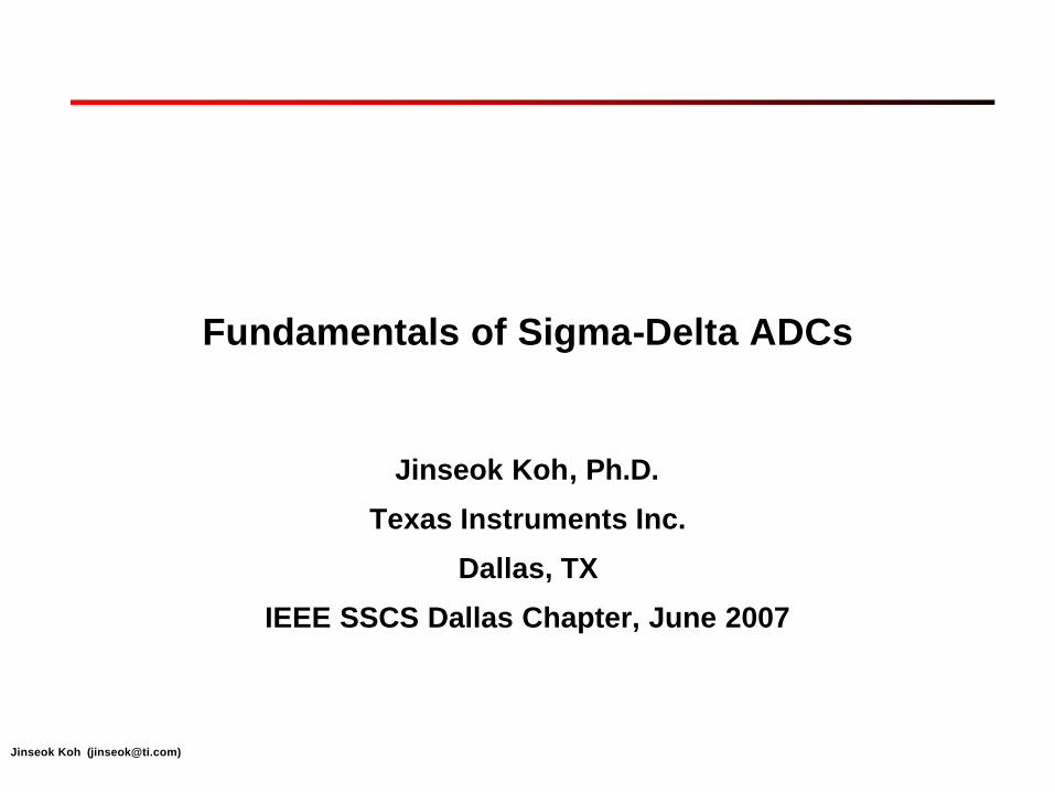
Why Analog to Digital Conversion?
ü Naturally occurring signals are analog signalü Human beings perceive and retain information in analog formü BUT, Analog signal is more sensitive to noise than digital signal
Jinseok Koh ([email protected])
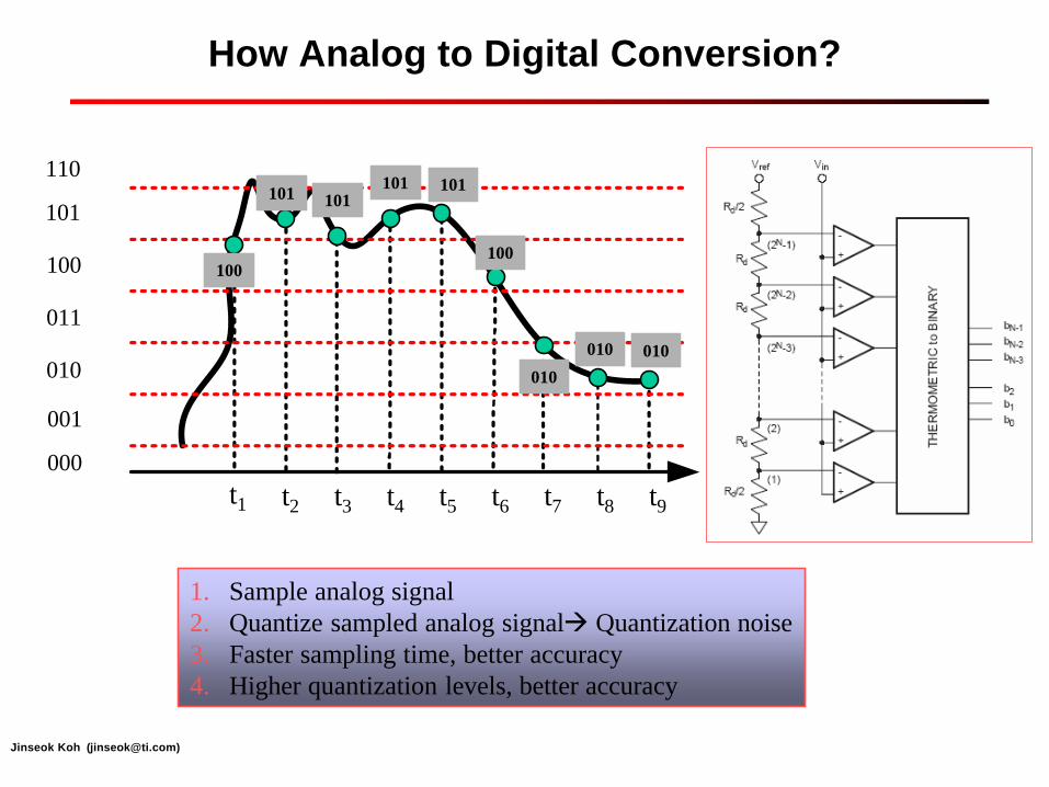
How Analog to Digital Conversion?
1. Sample analog signal2. Quantize sampled analog signalà Quantization noise3. Faster sampling time, better accuracy4. Higher quantization levels, better accuracy
t1 t2 t3 t4 t5 t6 t7 t8 t9
000
001
010
011
100
101
110101
100
101 101101
100
010
010 010
Jinseok Koh ([email protected])
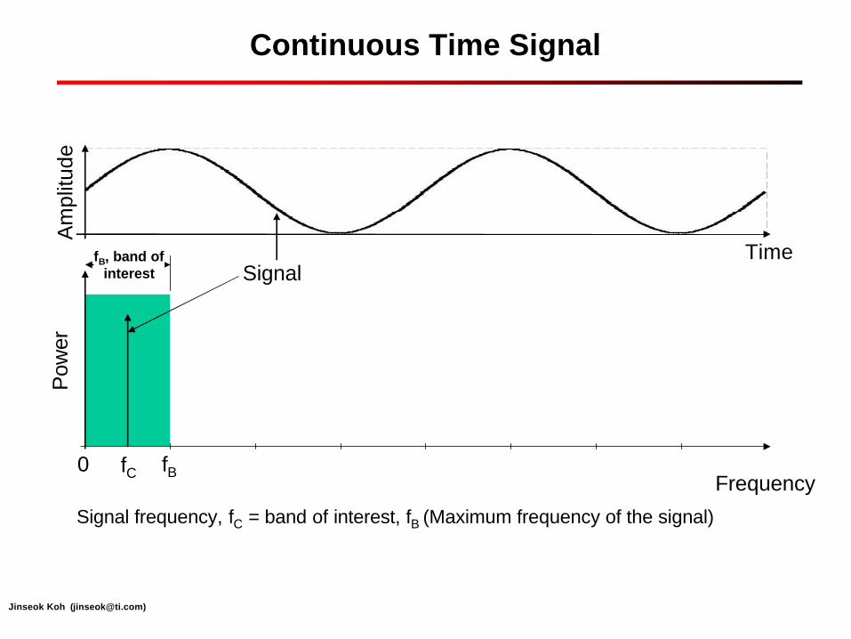
Continuous Time Signal
Time
Am
plitu
de
0 fBFrequency
Pow
er
fB, band ofinterest
Signal frequency, fC = band of interest, fB (Maximum frequency of the signal)
fC
Signal

Jinseok Koh ([email protected])
Jinseok Koh ([email protected])
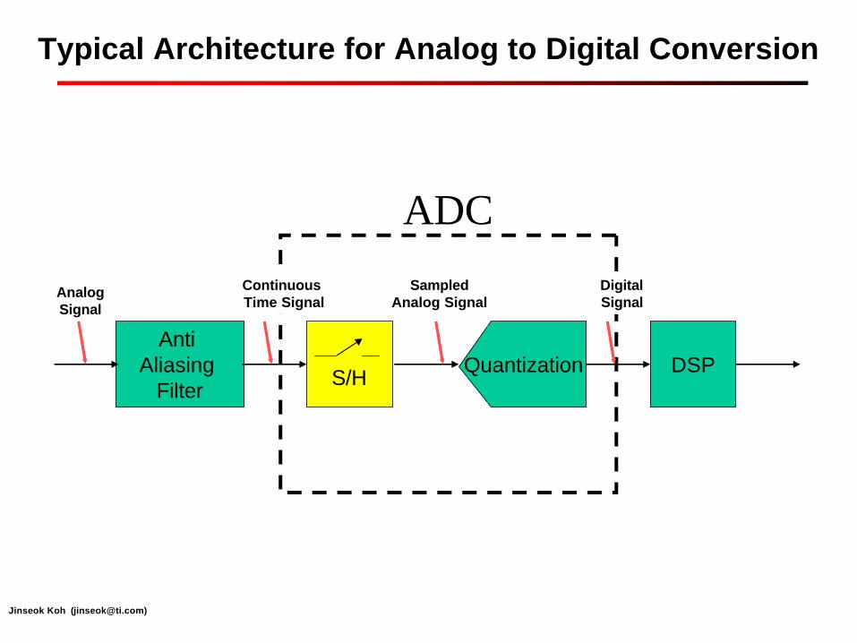
Anti Aliasing
Filter S/H Quantization DSP
AnalogSignal
SampledAnalog Signal
Continuous Time Signal
Typical Architecture for Analog to Digital Conversion
ADC
DigitalSignal
Jinseok Koh ([email protected])
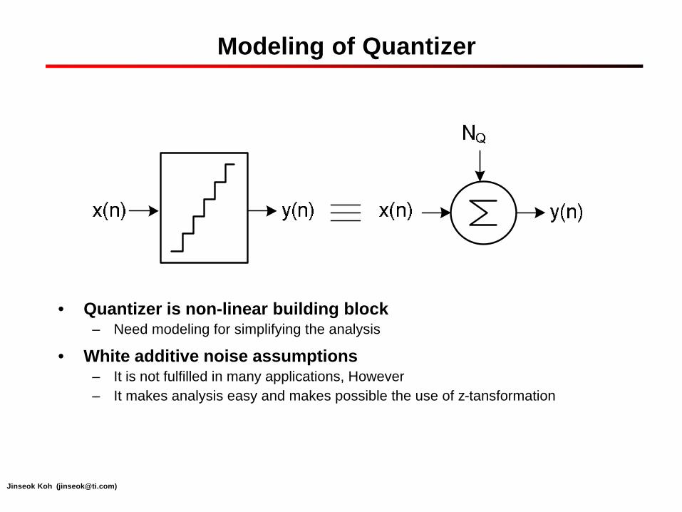
Modeling of Quantizer
• Quantizer is non-linear building block– Need modeling for simplifying the analysis
• White additive noise assumptions– It is not fulfilled in many applications, However– It makes analysis easy and makes possible the use of z-tansformation
Jinseok Koh ([email protected])
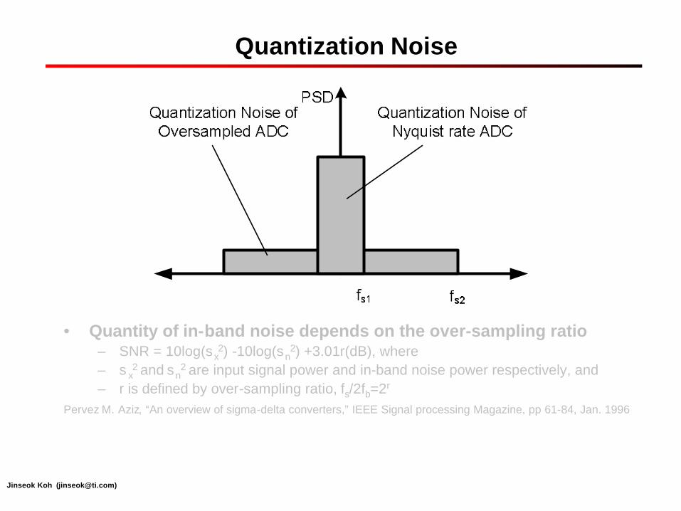
Quantization Noise
• Quantity of in-band noise depends on the over-sampling ratio– SNR = 10log(sx
2) -10log(sn2) +3.01r(dB), where
– s x2 and sn
2 are input signal power and in-band noise power respectively, and – r is defined by over-sampling ratio, fs/2fb=2r
Pervez M. Aziz, “An overview of sigma-delta converters,”IEEE Signal processing Magazine, pp 61-84, Jan. 1996
Jinseok Koh ([email protected])
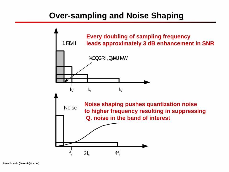
Over-sampling and Noise Shaping
IV IV IV
%DQG�RI�,QWHUHVW
1 RLVHEvery doubling of sampling frequencyleads approximately 3 dB enhancement in SNR
Noise shaping pushes quantization noise to higher frequency resulting in suppressing Q. noise in the band of interest
Jinseok Koh ([email protected])
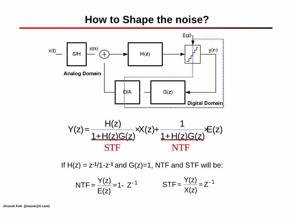
How to Shape the noise?
E(z)H(z)G(z)1
1X(z)
H(z)G(z)1H(z)
Y(z) ⋅+
+⋅+
=
If H(z) = z-1/1-z-1 and G(z)=1, NTF and STF will be:
STF NTF
1ZX(z)Y(z)
STF −==1Z1E(z)Y(z)
NTF −−==

Jinseok Koh ([email protected])

Jinseok Koh ([email protected])

Jinseok Koh ([email protected])
Jinseok Koh ([email protected])
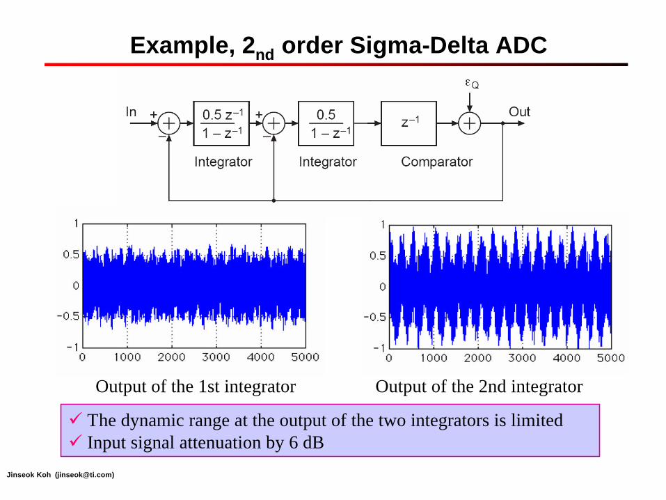
Example, 2nd order Sigma-Delta ADC
Output of the 1st integrator Output of the 2nd integrator
ü The dynamic range at the output of the two integrators is limitedü Input signal attenuation by 6 dB
Jinseok Koh ([email protected])
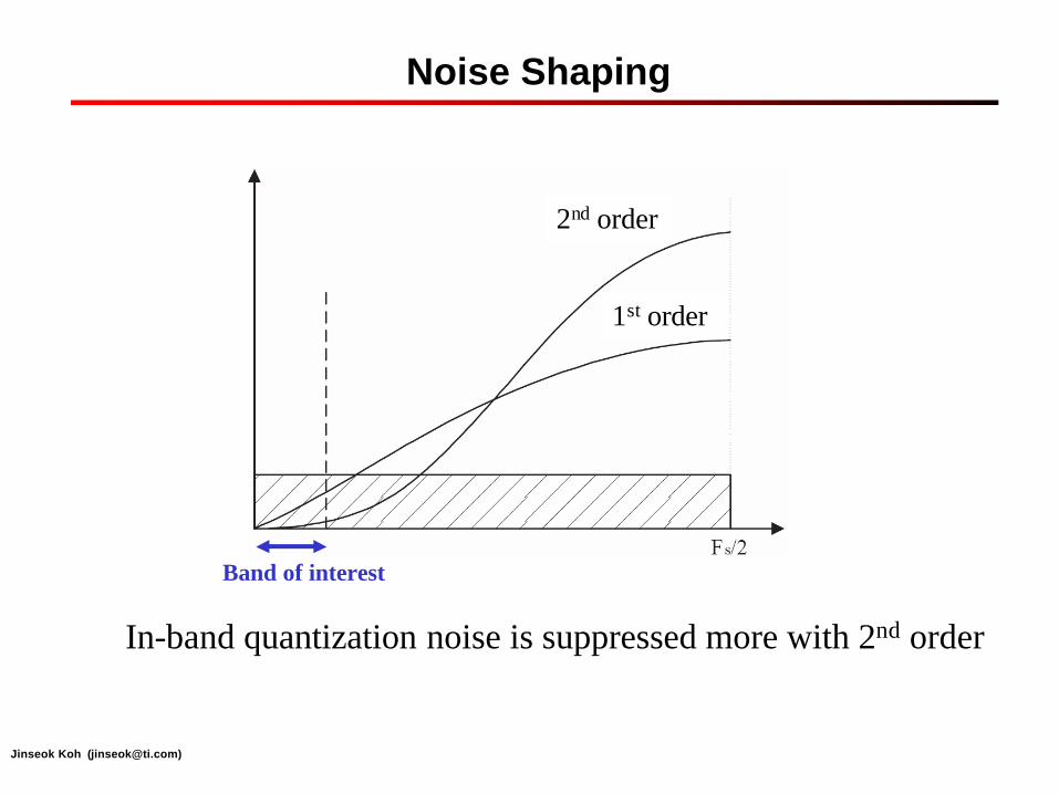
Noise Shaping
2nd order
1st order
Band of interest
In-band quantization noise is suppressed more with 2nd order
Jinseok Koh ([email protected])
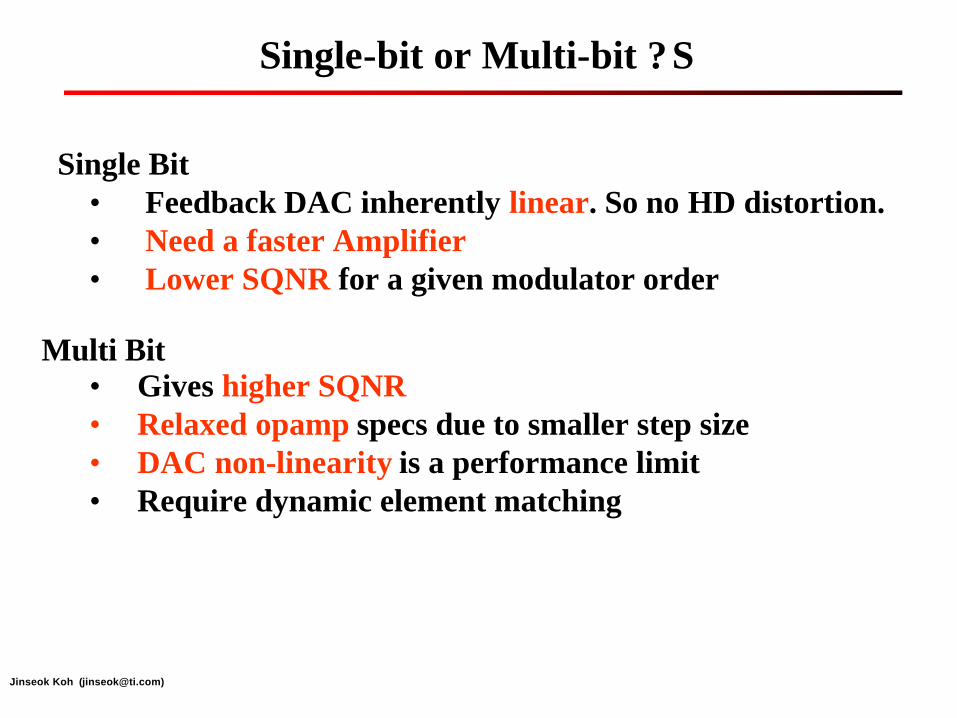
Single-bit or Multi-bit ?S
Single Bit• Feedback DAC inherently linear. So no HD distortion. • Need a faster Amplifier• Lower SQNR for a given modulator order
Multi Bit• Gives higher SQNR• Relaxed opamp specs due to smaller step size• DAC non-linearity is a performance limit• Require dynamic element matching
Jinseok Koh ([email protected])
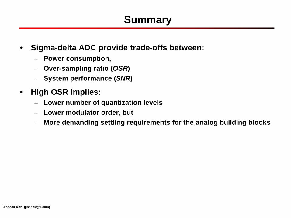
Summary
• Sigma-delta ADC provide trade-offs between:– Power consumption,– Over-sampling ratio (OSR)– System performance (SNR)
• High OSR implies:– Lower number of quantization levels – Lower modulator order, but– More demanding settling requirements for the analog building blocks
Jinseok Koh ([email protected])
A Sigma-Delta ADC with a built-in Anti-aliasing filter for Bluetooth receiver in 130 nm digital process
Jinseok Koh
Wireless Analog Technology Center
Texas Instruments Inc.
Dallas, TX
Published in CICC2004
Jinseok Koh ([email protected])
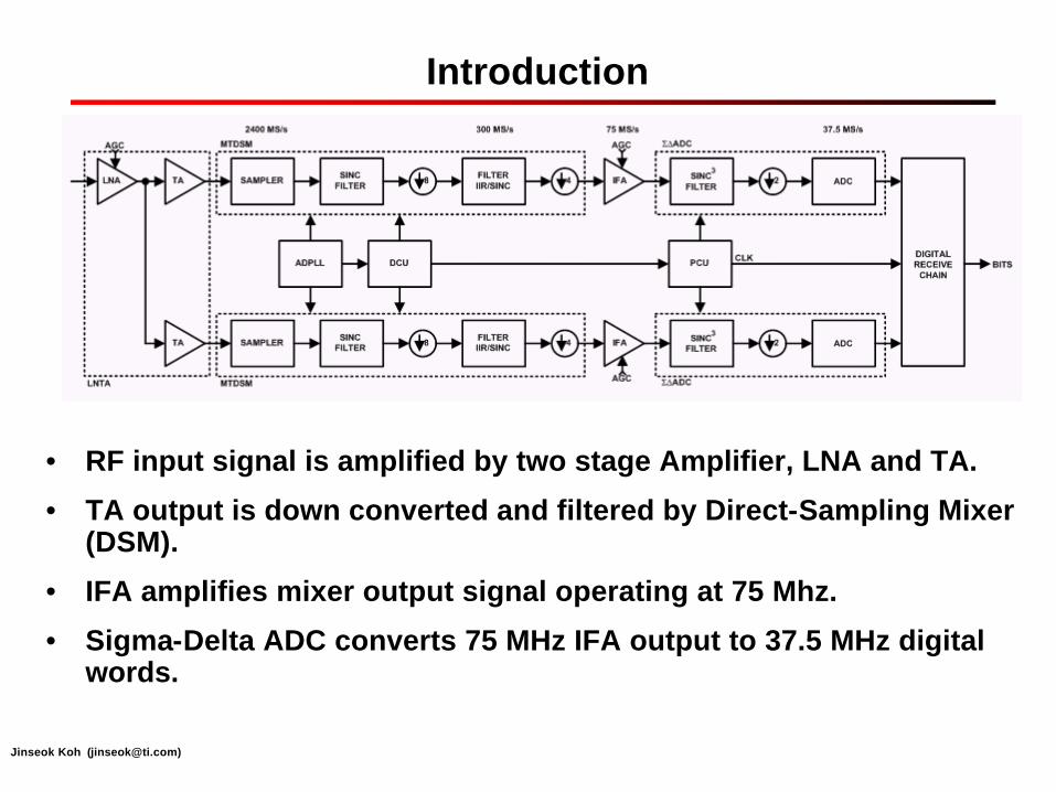
Introduction
• RF input signal is amplified by two stage Amplifier, LNA and TA.
• TA output is down converted and filtered by Direct-Sampling Mixer (DSM).
• IFA amplifies mixer output signal operating at 75 Mhz.
• Sigma-Delta ADC converts 75 MHz IFA output to 37.5 MHz digital words.
Jinseok Koh ([email protected])
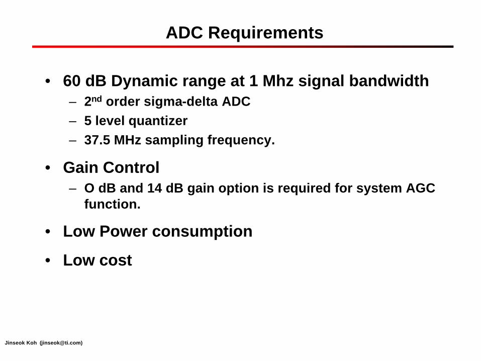
ADC Requirements
• 60 dB Dynamic range at 1 Mhz signal bandwidth– 2nd order sigma-delta ADC – 5 level quantizer – 37.5 MHz sampling frequency.
• Gain Control– O dB and 14 dB gain option is required for system AGC
function.
• Low Power consumption
• Low cost
Jinseok Koh ([email protected])
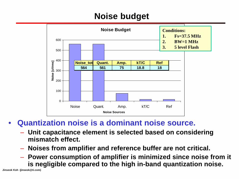
Noise budget
• Quantization noise is a dominant noise source.– Unit capacitance element is selected based on considering
mismatch effect.– Noises from amplifier and reference buffer are not critical. – Power consumption of amplifier is minimized since noise from it
is negligible compared to the high in-band quantization noise.
(unit = µV)
Noise Budget
0
100
200
300
400
500
600
Noise Quant. Amp. kT/C RefNoise Sources
Noi
se [
uVrm
s] Noise_tot Quant. Amp. kT/C Ref564 561 75 18.8 18
Conditions:1. Fs=37.5 MHz2. BW=1 MHz3. 5 level Flash
Jinseok Koh ([email protected])
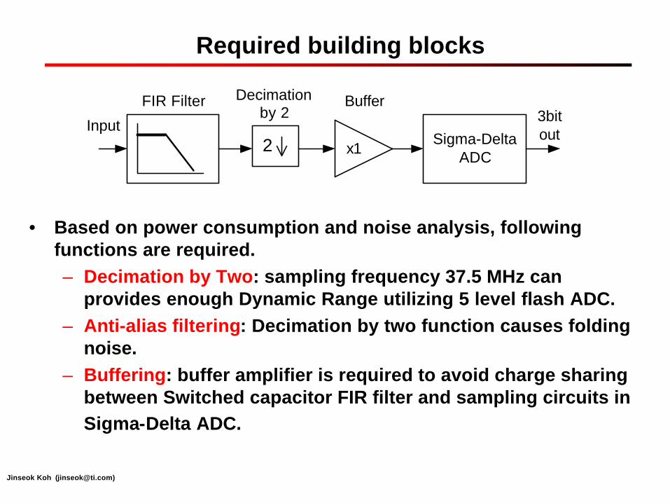
Required building blocks
• Based on power consumption and noise analysis, following functions are required.– Decimation by Two: sampling frequency 37.5 MHz can
provides enough Dynamic Range utilizing 5 level flash ADC. – Anti-alias filtering: Decimation by two function causes folding
noise. – Buffering: buffer amplifier is required to avoid charge sharing
between Switched capacitor FIR filter and sampling circuits in Sigma-Delta ADC.
Sigma-DeltaADC
FIR Filter
2 x1
Decimationby 2
Buffer3bitoutInput
Jinseok Koh ([email protected])
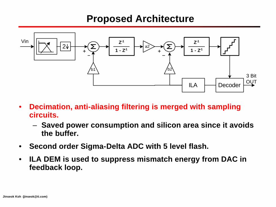
Proposed Architecture
• Decimation, anti-aliasing filtering is merged with sampling circuits.– Saved power consumption and silicon area since it avoids
the buffer.
• Second order Sigma-Delta ADC with 5 level flash.
• ILA DEM is used to suppress mismatch energy from DAC in feedback loop.
2Vin Z-1
1 - Z-1
Z-1
1 - Z-1a2
b2b1
3 BitOUT
DecoderILA
Jinseok Koh ([email protected])
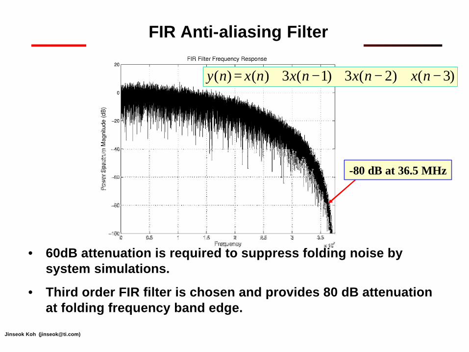
FIR Anti-aliasing Filter
• 60dB attenuation is required to suppress folding noise by system simulations.
• Third order FIR filter is chosen and provides 80 dB attenuation at folding frequency band edge.
)3()2(3)1(3)()( −+−+−+= nxnxnxnxny
-80 dB at 36.5 MHz
Jinseok Koh ([email protected])
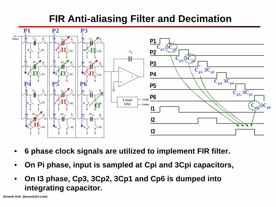
FIR Anti-aliasing Filter and Decimation
• 6 phase clock signals are utilized to implement FIR filter.
• On Pi phase, input is sampled at Cpi and 3Cpi capacitors,
• On I3 phase, Cp3, 3Cp2, 3Cp1 and Cp6 is dumped into integrating capacitor.
P1
P2
P3
P4
P5
P6
I1
I2
I3
5 levelDAC
Vrefp
Vrefm
Input
CM
P1
P1
P1
P1 P2
P2
P2
P2
P3
P3
P4
P4
P4
P4 P5
P5
P5
P5
P6
P6
P6
P6
I2
I3
I1
I3
I3
I3
I1
I1P3
P3
I3
I3
I2
I2
I2
I1
I1
I2
I2 I1
I1
I2
I2 I1
I3 I3
Cp1
3Cp1
Cp2
3Cp2
Cp3
3Cp3
Cp5
3Cp5
Cp6
3Cp6
Cp4
3Cp4
P1 P2 P3
P4 P5 P6
I1
I1
I1
I1
I3
I3
I3
I3 Cp1, 3Cp1
Cp2, 3Cp2
Cp4, 3Cp4
Cp3, 3Cp3
Cp5, 3Cp5
Cp6, 3Cp6
Jinseok Koh ([email protected])
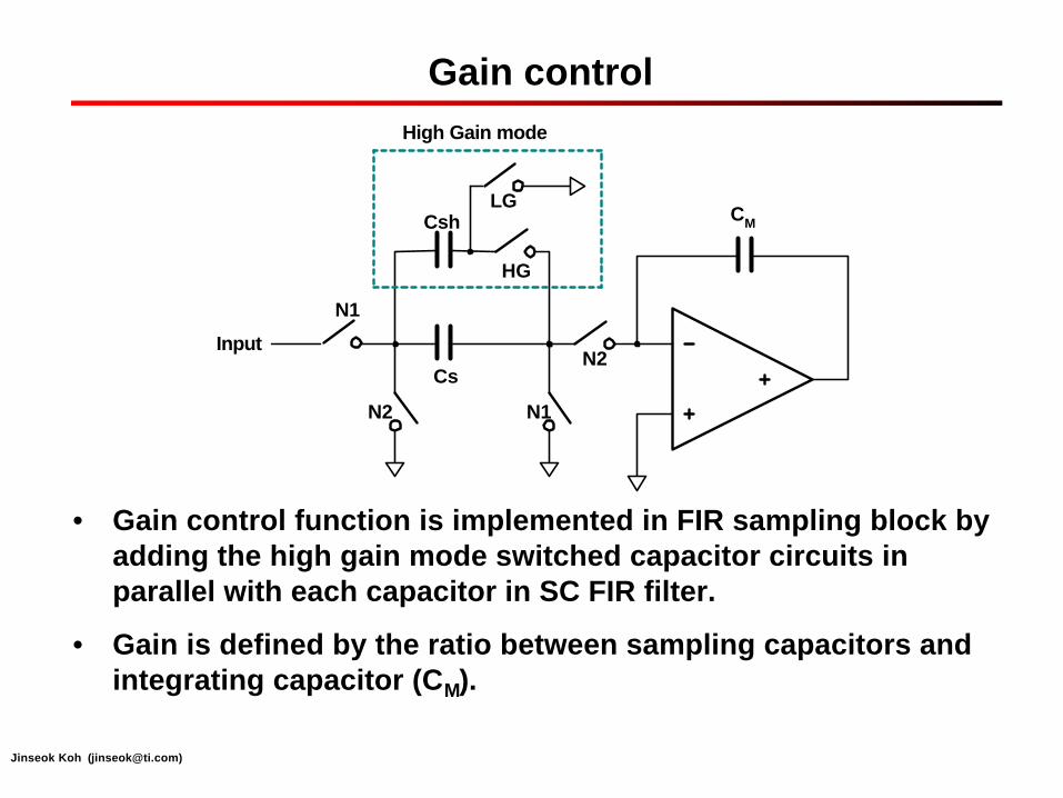
Gain control
• Gain control function is implemented in FIR sampling block by adding the high gain mode switched capacitor circuits in parallel with each capacitor in SC FIR filter.
• Gain is defined by the ratio between sampling capacitors and integrating capacitor (CM).
CM
HG
High Gain mode
N1
N1
LG
N2
N2
Cs
Csh
Input
Jinseok Koh ([email protected])
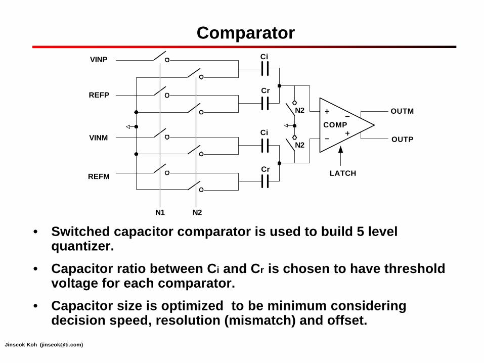
Comparator
• Switched capacitor comparator is used to build 5 level quantizer.
• Capacitor ratio between Ci and Cr is chosen to have threshold voltage for each comparator.
• Capacitor size is optimized to be minimum considering decision speed, resolution (mismatch) and offset.
VINP
VINM
REFP
REFM
COMP
Cr
Cr
Ci
Ci
N1 N2
N2
N2OUTP
OUTM
LATCH
Jinseok Koh ([email protected])
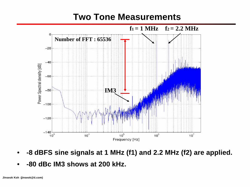
Two Tone Measurements
• -8 dBFS sine signals at 1 MHz (f1) and 2.2 MHz (f2) are applied.
• -80 dBc IM3 shows at 200 kHz.
Number of FFT : 65536
f1 = 1 MHz f2 = 2.2 MHz
IM3
Jinseok Koh ([email protected])
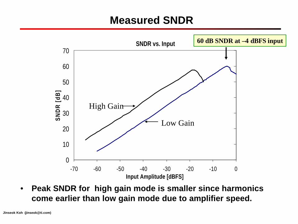
SNDR vs. Input
0
10
20
30
40
50
60
70
-70 -60 -50 -40 -30 -20 -10 0Input Amplitude [dBFS]
SN
DR
[dB
]
High Gain
Low Gain
Measured SNDR
• Peak SNDR for high gain mode is smaller since harmonics come earlier than low gain mode due to amplifier speed.
60 dB SNDR at –4 dBFS input
Jinseok Koh ([email protected])
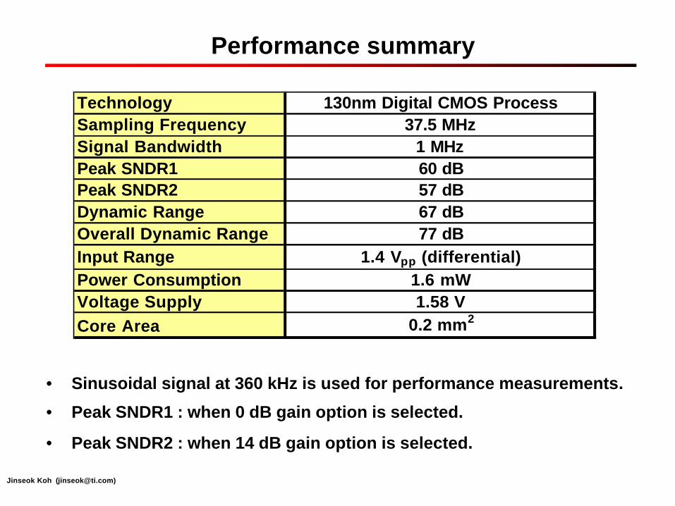
Performance summary
• Sinusoidal signal at 360 kHz is used for performance measurements.
• Peak SNDR1 : when 0 dB gain option is selected.
• Peak SNDR2 : when 14 dB gain option is selected.
Technology 130nm Digital CMOS ProcessSampling Frequency 37.5 MHzSignal Bandwidth 1 MHzPeak SNDR1 60 dBPeak SNDR2 57 dBDynamic Range 67 dBOverall Dynamic Range 77 dBInput Range 1.4 Vpp (differential)Power Consumption 1.6 mWVoltage Supply 1.58 VCore Area 0.2 mm2
Jinseok Koh ([email protected])
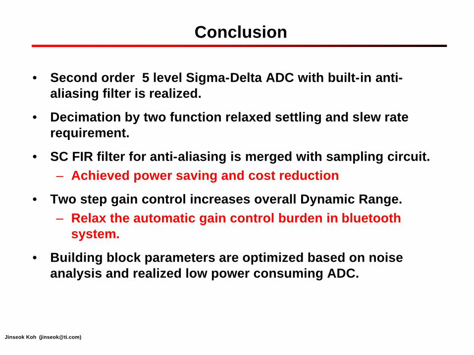
Conclusion
• Second order 5 level Sigma-Delta ADC with built-in anti-aliasing filter is realized.
• Decimation by two function relaxed settling and slew rate requirement.
• SC FIR filter for anti-aliasing is merged with sampling circuit. – Achieved power saving and cost reduction
• Two step gain control increases overall Dynamic Range.– Relax the automatic gain control burden in bluetooth
system.
• Building block parameters are optimized based on noise analysis and realized low power consuming ADC.
Jinseok Koh ([email protected])
66dB DR 1.2V 1.2mW Single-AmplifierDouble-Sampling 2nd-order ?S ADC for
WCDMA in 90nm CMOS
Jinseok Koh
Wireless Analog Technology Center
Texas Instruments Inc.
Dallas, TX
Published in ISSCC2005
Jinseok Koh ([email protected])
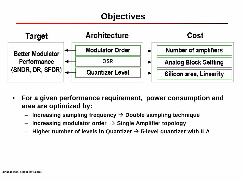
Objectives
• For a given performance requirement, power consumption and area are optimized by: – Increasing sampling frequency à Double sampling technique– Increasing modulator order à Single Amplifier topology– Higher number of levels in Quantizer à 5-level quantizer with ILA
Jinseok Koh ([email protected])
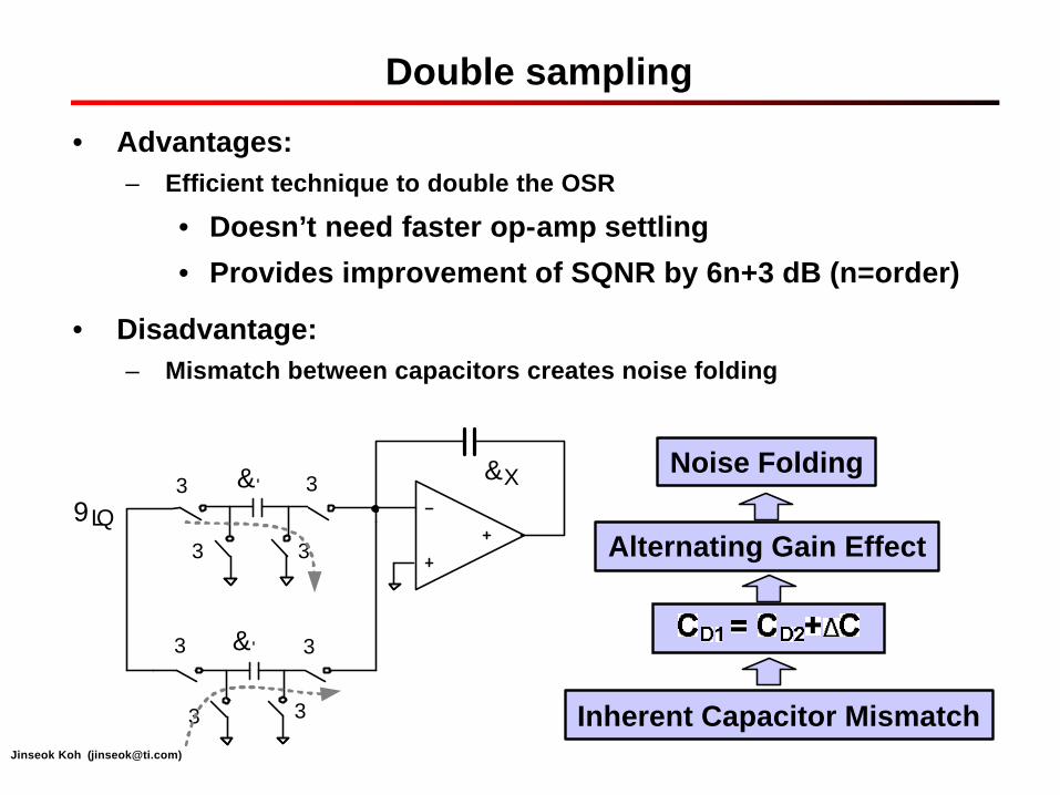
Double sampling
• Advantages:– Efficient technique to double the OSR
• Doesn’t need faster op-amp settling
• Provides improvement of SQNR by 6n+3 dB (n=order)
• Disadvantage: – Mismatch between capacitors creates noise folding
9LQ3
3
3
3
3
3
3
3
& '
& '
&X
Inherent Capacitor Mismatch
Alternating Gain Effect
Noise Folding
Jinseok Koh ([email protected])
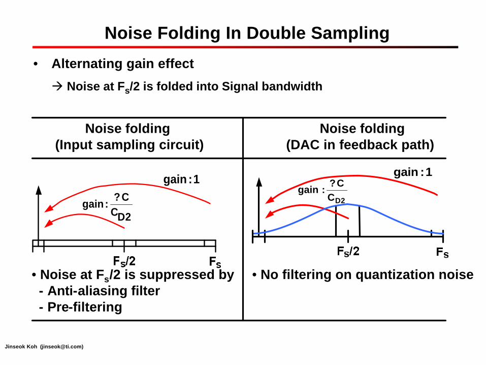
Noise Folding In Double Sampling
• Alternating gain effect
à Noise at Fs/2 is folded into Signal bandwidth
D2C?C
:gain
1:gain
Noise folding (Input sampling circuit)
Noise folding(DAC in feedback path)
D2C?C
:gain
1:gain
•Noise at Fs/2 is suppressed by- Anti-aliasing filter- Pre-filtering
•No filtering on quantization noise
Jinseok Koh ([email protected])
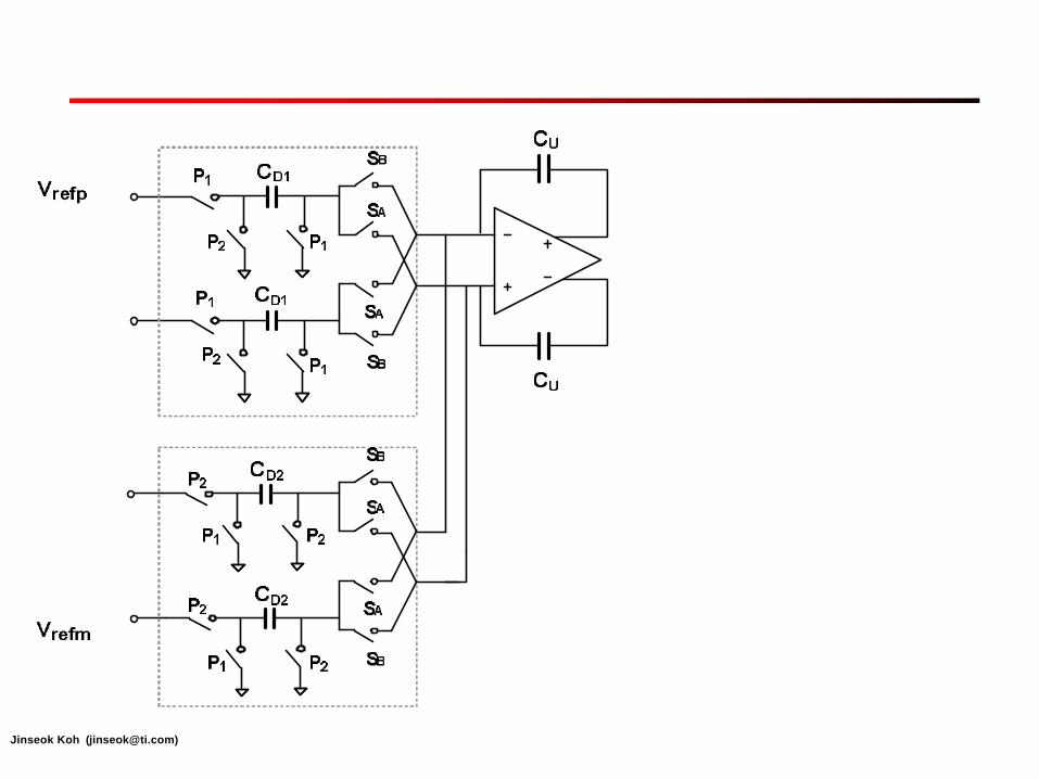
Conventional Double Sampling DAC
• Requires two sets of switched capacitor DACs
• Mismatch on stored charge causes alternating gain effect
• On P1 phase,Stored charge in CD1 :
CD1(Vrefp-Vrefm)
•On P2 phase,
Stored charge in CD2 :CD2(Vrefp-Vrefm)
Jinseok Koh ([email protected])
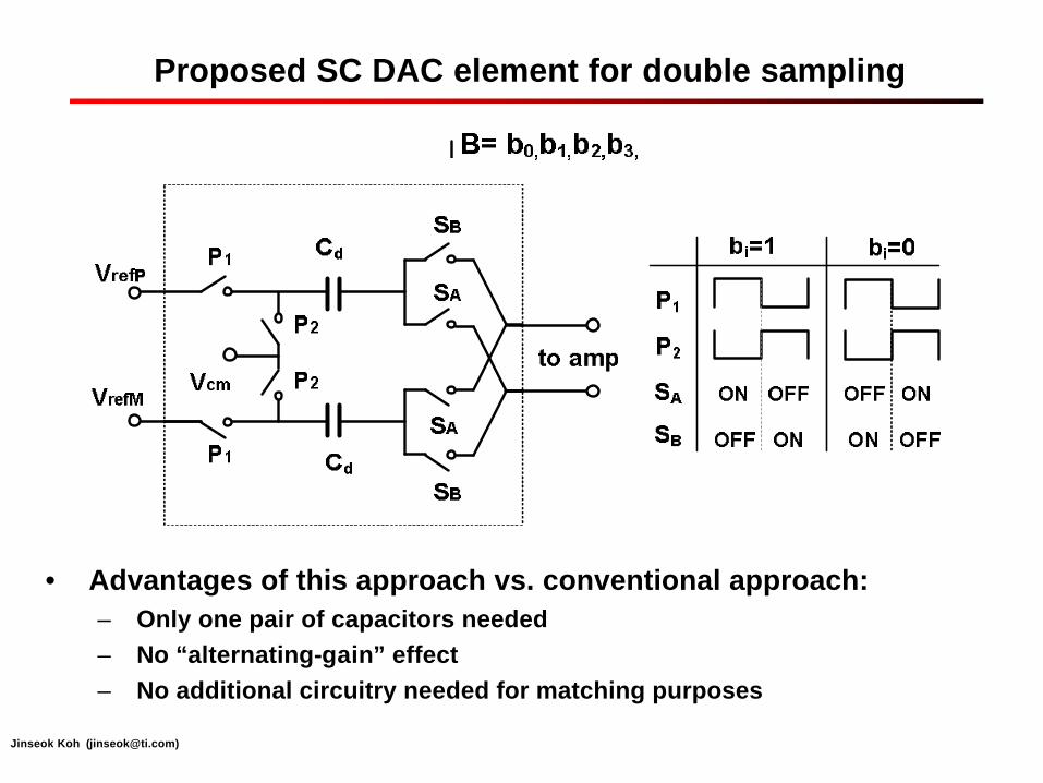
• Advantages of this approach vs. conventional approach:– Only one pair of capacitors needed– No “alternating-gain”effect– No additional circuitry needed for matching purposes
Proposed SC DAC element for double sampling
Jinseok Koh ([email protected])
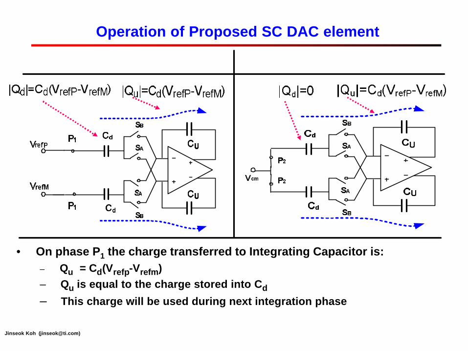
• On phase P1 the charge transferred to Integrating Capacitor is:– Qu = Cd(Vrefp-Vrefm)– Qu is equal to the charge stored into Cd
– This charge will be used during next integration phase
Operation of Proposed SC DAC element
On P1 Phase: On P2 Phase:
Jinseok Koh ([email protected])
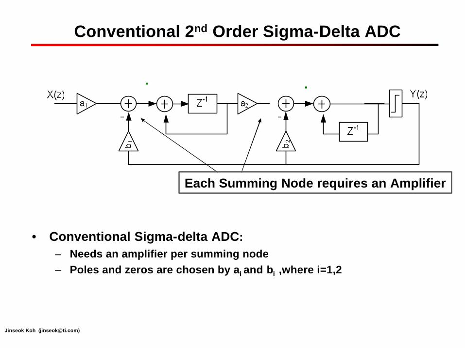
• Conventional Sigma-delta ADC:– Needs an amplifier per summing node– Poles and zeros are chosen by ai and bi ,where i=1,2
Conventional 2nd Order Sigma-Delta ADC
Each Summing Node requires an Amplifier
Jinseok Koh ([email protected])
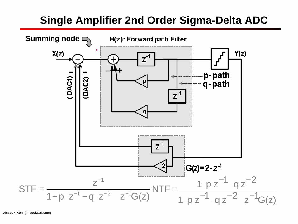
G(z)1z2zq1zp1
2zq1zp1NTF−+−⋅−−⋅−
−⋅−−⋅−=G(z)zzqzp1
zSTF 121
1
−−−
−
+⋅−⋅−=
Summing node
Single Amplifier 2nd Order Sigma-Delta ADC
Jinseok Koh ([email protected])
SNDR vs. Input
0
10
20
30
40
50
60
70
-70 -60 -50 -40 -30 -20 -10 0
Input Amplitude [dBFS]
SN
DR
[dB
]
SNDR vs. Input power
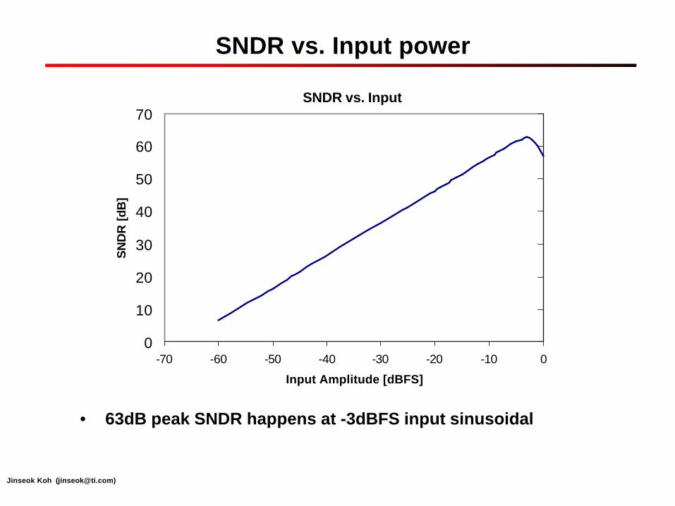
• 63dB peak SNDR happens at -3dBFS input sinusoidal
Jinseok Koh ([email protected])
I-channel Q-channel
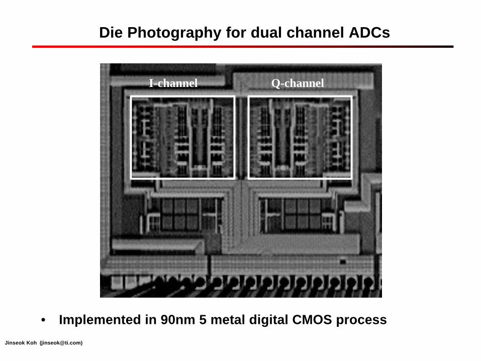
Die Photography for dual channel ADCs
• Implemented in 90nm 5 metal digital CMOS process
Jinseok Koh ([email protected])
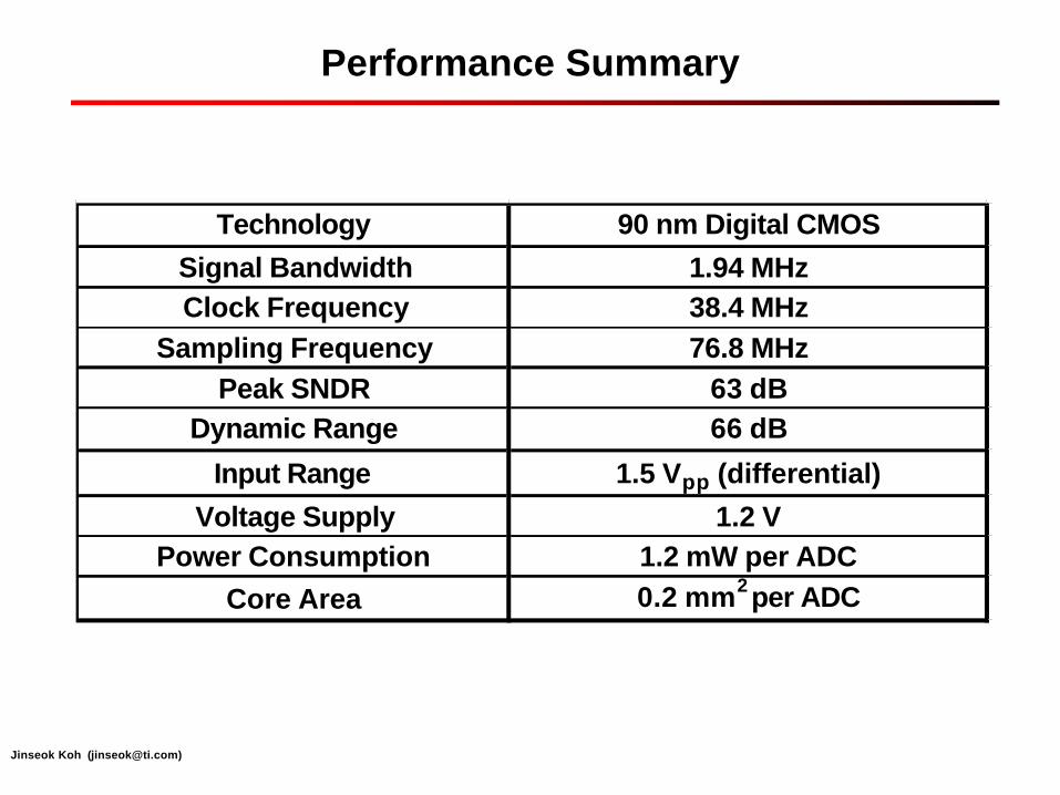
Technology 90 nm Digital CMOS
Signal Bandwidth 1.94 MHzClock Frequency 38.4 MHz
Sampling Frequency 76.8 MHzPeak SNDR 63 dB
Dynamic Range 66 dB
Input Range 1.5 Vpp (differential)
Voltage Supply 1.2 VPower Consumption 1.2 mW per ADC
Core Area 0.2 mm2 per ADC
Performance Summary
Jinseok Koh ([email protected])
Conclusions
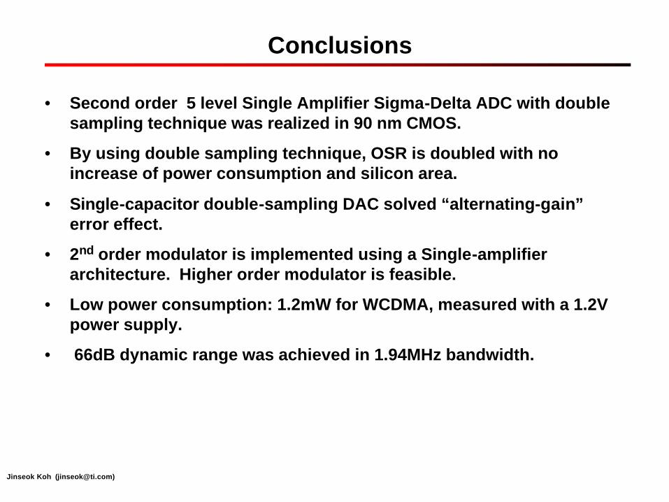
• Second order 5 level Single Amplifier Sigma-Delta ADC with double sampling technique was realized in 90 nm CMOS.
• By using double sampling technique, OSR is doubled with no increase of power consumption and silicon area.
• Single-capacitor double-sampling DAC solved “alternating-gain”error effect.
• 2nd order modulator is implemented using a Single-amplifier architecture. Higher order modulator is feasible.
• Low power consumption: 1.2mW for WCDMA, measured with a 1.2V power supply.
• 66dB dynamic range was achieved in 1.94MHz bandwidth.