Embed Size (px)
Citation preview

r.ANALOG ~DEVICES
AN-283 APPLICATION NOTE
ONE TECHNOLOGY WAY • P.O. BOX 9106 • NORWOOD, MASSACHUSETIS 02062-9106 • 617/329-4700
Sigma-Delta ADCs and DACs
SIGMA-DELTA OVERVIEW Within the last several years, the sigma
delta architecture has become more and more popular for realizing high-resolutionADCs in mixed-signal VLSI processes. Until recently, however, the process technology needed to make these devices commercially viable has not been available. Now that 1 micron and smaller CMOS geometries are manufactureable, sigma-delta converters will become even more prolific in certain types of applications, especially mixed-signal ICs which combine theADC, DAC, and DSP functions on a single chip.
Conceptually, the sigma-delta architecture is more digital than analog intensive. This does not, however, minimize the importance of the analog portion ofthe sigma-deltaADC. The design of a fifth-order sigma-delta modulator (as in the AD1879 duall8 bit ADC) is certainly not a trivial matter, and neither is the digital filter. The sigma-delta converter is inherently an oversampling converter, although oversampling is just one of the techniques contributing to the overall performance. Basically, a sigma-delta converter digitizes an analog signal with a very low
SIGMA-DELTA CONCEPTS
• Ideal Topology for Mixed Signal VLSI Chips
• Oversampling
• Noise-Spectrum Shaping Using Sigma-Delta Modulator
• Digital Filtering
• Decimation
• 16-Bits and Higher Resolution Possible
Figure 6.1
resolution (1 bit)ADC at a very high sampling rate. By using oversampling techniques in conjunction with noise shaping and digital filtering, the effective resolution is increased. Decimation is then used to reduce the effective sampling rate at the ADC output. The sigma-delta ADC exhibits excellent differential and integral linearity due to the linearity of the 1 bit quantizer and DAC, and no trimming is required as in other ADC architectures.
The key concepts involved in understanding the operation of sigma-delta converters are oversampling, noise shaping (using a sigma-delta modulator), digital filtering, and decimation.
0VERSAMPLING
The concept of oversampling has been previously discussed in Section III, and is illustrated again in Figure 6.2 and 6.3. As was
NYQUIST SAMPLING WITH ANALOG LOWPASS FILTER
ANALOG LOW PASS ~ ADC
FILTER
~ass= fa i, s
fstop = fs 12
Figure 6.2
DIGITAL SIGNAL
L /
DATA RA TE = f s

OVERSAMPLING WITH ANALOG AND DIGITAL FILTERING
DIGITAL ANALOG LOW PASS
FILTER ADC LOWPASS "---r---'L FILTER
DECIMATE
DATA RATE= Kf8
BYK I 1 DATA RATE = f8~
fstop = Kfs /2 Kfs
K = OVERSAMPLING RATIO (INTEGER)
rDIGITAL FILTER
discussed, one significant benefit of oversampling is that the rolloff requirements on the analog antialiasing filter are relaxed. The quantization noi~e (rms value over Nyquist bandwidth is qJ 12 , where q is the weight of the LSB) which falls between f
8/2 and kf/2
is removed from the output by the digital filter (k is the oversampling ratio). This has the effect of increasing the overall signal-tonoise ratio by an amount equal to 10log10(k). Unfortunately this is a high price to pay for extra resolution, as an oversampling ratio of 4 is required just to increase the signal-tonoise ratio by a modest 6d.B ( 1 bit). 'lb keep the oversampling ratio within reasonable bounds, it is possible to shape the frequency spectrum of the quantization noise so that the majority of the noise lies between f /2 and kf/2, and only a small portion is l;ft
2
QUANTIZATION NOISE REMOVED BY
DIGITAL FILTER
Figure 6.3
between de and fj2. This is precisely what a sigma-delta modUlator does in a sigma-delta ADC. After the noise spectrum is shaped by the modulator, the digital filter can then remove the bulk of the quantization noise energy, and the overall signal-to-noise ratio (hence the dynamic range) is dramatically increased.
SIGMA-DELTA MODULATORS AND QUANTIZATION NOISE SHAPING
A block diagram of a first-order sigmadeltaADC is shown in Figure 6.4. The first part of the converter is the sigma-delta modulator which converts the input signal into a continuous serial stream of l's and O's at a rate determined by the sampling clock
FIRST -ORDER SIGMA-DELTA ADC -.-.-.-.- ·-·-.-. -·-.-. ---· -·-·- ·- ·-·-·-·-· -· -·-· -· -· -·- ·-.- ·-1 CLOCK
Kf8
LATCHED COMPARATOR
(1 BITADC)
1 BIT DATA STREAM
Figure 6.4
DIGITAL FILTER
AND DECIMA TOR
1 BIT, Kf8
N BITS

SIGMA-DELTA MODULATOR WAVEFORMS
\'IN= OV = 2/4 = 4/8
1\l\1\l\l\/\ A/VVVVV\
INTEGRATOR OUTPUT
B COMPARATOR OUTPUT
010101010101
COMPARATOR OUTPUT
= 3/4
= 6/8 0111011101110
frequency, kf. The 1-bit DAC is driven by the serial output data stream, and the DAC output is subtracted from the input signal. Feedback control theory tells us that the average value of the DAC output (hence the serial bit stream) must approach that of the input signal if the loop has enough gain. The integrator can be represented in the frequency domain by a filter whose amplitude response is proportional to 1/f, where fis the input frequency. Since the chopper-like action of the clocked, latched comparator converts the input signal to a high-frequency ac signal, varying about the average value of the input, the effective quantization noise at low frequencies is greatly reduced (the integrator looks like a high-pass filter to quantization noise). The exact frequency spectrum of the resulting noise depends on the sampling rate, the integrator time constant, and the precise span of the voltage fed back.
For any given input value in a single sampling interval, the data from the 1-bit ADC is virtually meaningless. Only when a large number of samples are averaged, will a meaningful value result. The sigma-delta modulator is very difficult to analyze in the time domain because of this apparent randomness of the single-bit data output. If the input signal is near positive fullscale, it is clear that there will be more l's than O's in the bit stream. Likewise, for signals near negative fullscale, there will be more O's than l's in the bit stream. For signals near midscale, there will be approximately an equal number of l's and O's. Figure 6.5 shows the output of the integrator for two input conditions. The first is for an input of zero (midscale). To decode the output, pass the output samples through a simple digital lowpass filter that averages every four samples. The output of the filter is 2/4. This value represents bipolar zero. If more samples are averaged, more dynamic range
Figure 6.5
is achieved. For example, averaging 4 samples gives 2 bits of resolution, while averaging 8 samples yields 4/8, or 3 bits of resolution. In the bottom waveform ofFigure 6.5, the average obtained for 4 samples is 3/4, and the average for 8 samples is 6/8.
The sigma-delta ADC can also be viewed as a synchronous voltage-to-frequency converter followed by a counter. If the number of·l's in the output data stream is counted over a sufficient number of samples, the counter output will represent the digital value ofthe input. Obviously,_ this method of averaging will only work for de or very slowly changing input signals. In addition, 2N clock cycles must be counted in order to achieve Nbit effective resolution, thereby severely limiting the effective sampling rate.
Further analysis of the sigma-delta architecture is best done in the frequency domain using the linear model shown in Figure 6.6. Note that the integrator is represented as an analog filter with a given transfer function H(O. The transfer function has an amplitude response which is inversely proportional to the input frequency. The quantizer is modeled as a gain stage followed by the addition of quantization noise. One of the advantages of using frequency domain analysis is that algebra can be used to describe the signals. The output value y can be represented as the difference x - y from the summing node at the input multiplied by the transfer function of the analog filter (integrator), multiplied by the gain block, and then added with the quantization noise Q. If we set the gain to 1, and the transfer function is represented as 1/f, the following mathematical relationship results: ~ y = + Q, or by""'rearranging,
f
y=-x-+ _gf_ f+l f+l
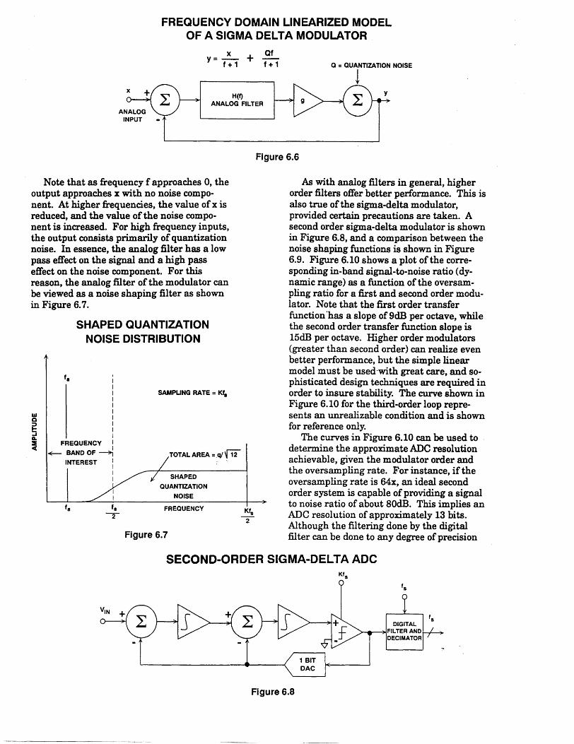
FREQUENCY DOMAIN LINEARIZED MODEL OF A SIGMA DELTA MODULATOR
X + ~ Y= f+1 f+1
H{f) ANALOG FILTER
Q =QUANTIZATION NOISE
l
Figure 6.6
Note that as frequency f approaches 0, the output approaches x with no noise component. At higher frequencies, the value ofx is reduced, and the value of the noise component is increased. For high frequency inputs, the output consists primarily of quantization noise. In essence, the analog filter has a low pass effect on the signal and a high pass effect on the noise component. For this reason, the analog filter of the modulator can be viewed as a noise shaping filter as shown in Figure 6. 7.
SHAPED QUANTIZATION NOISE DISTRIBUTION
I
I I I I I
UJ I 0 : 5 I D. I ~ FREQUENCY I
c( ~BAND OF~ INTEREST :
I I
'· -2-
SAMPUNG RATE = Kfs
TOTAL AREA =.q/f12
SHAPED
QUANTIZATION
NOISE
FREQUENCY
Figure 6.7
As with analog filters in general, higher order filters offer better performance. This is also true of the sigma-delta modulator, provided certain precautions are taken. A second order sigma-delta modulator is shown in Figure 6.8, and a comparison between the noise shaping functions is shown in Figure 6.9. Figure 6.10 shows a plot of the corresponding in-band signal-to-noise ratio (dynamic range) as a function of the oversampling ratio for a first and second order modulator. Note that the first order transfer function 'has a slope of 9d.B per octave, while the second order transfer function slope is 15d.B per octave. Higher order modulators (greater than second order) can realize even better performance, but the simple linear model must be used·with great care, and sophisticated design techniques are required in order to insure stability. The curve shown in Figure 6.10 for the third-order loop represents an unrealizable condition and is shown for reference only.
The curves in Figure 6.10 can be used to determine the approximate ADC resolution achievable, given the modulator order and the oversampling rate. For instance, if the oversampling rate is 64x, an ideal second order system is capable of providing a signal to noise ratio of about 80d.B. This implies an ADC resolution of approximately 13 bits. Although the filtering done by the digital filter can be done to any degree of precision
SECOND-ORDER SIGMA-DELTA ADC
Figure 6.8
DIGITAL FILTER AND DECIMA TOR

desirable, it would be pointless to carry more than 13 binary bits to the outside world. Additional bits would carry no useful signal information, and would be buried in noise.
FIRST AND SECOND-ORDER NOISE SHAPING FUNCTIONS
----------1 I I I I I I I
DIGITAL :
+---- FILTER -+I
PASSBAND :
I I I I
'· -2-
SAMPUNG RATE = Kfa
2nd ORDER
• t
1st ORDER
Figure 6.9
SNR VERSUS OVERSAMPLING RATIO FOR FIRST, SECOND, AND THIRD-ORDER LOOPS
120
100
80
SNR
(dB) 60
40
20
0 4 8
THIRD-ORDER LOOP*
* > 2nd QRDER LOOPS DO NOT
OBEY UNEAR MODEL
16 32 64 128 256 OVERSAMPUNG RATIO, K
Figure 6.10
DIGITAL FILTERING AND DECIMATION
After the quantization noise has been shaped by the modulator and pushed into the frequencies above the band of~terest, digital filtering techniques can be applied to this shaped quantization noise as shown in Figure 6.11. The purpose of the digital ~ter is twofold. First, it must act as an antialiasing filter with respect to the final sampling rate, f
8• Second, it must filter out the higher
frequency noise produced by the noiseshaping process of the sigma-delta modulator.
EFFECTS OF DIGITAL FILTERING ON SHAPED QUANTIZATION NOISE
----------1
BEFORE
DIGITAL
FILTERING
I FREQUENCY 1
+- BANDOF~ INTEREST l
I I
SAMPUNG RATE= Kfs
DIGITAL
'· -2-
SHAPED QUANTIZATION NOISE
Kf8 -2-
AFTER I FILTERING L-----,.4 __________ "1'--~
I fs Kf
8 2 -2-
Figure 6.11
The final data rate reduction is performed by digitally resampling the filtered output using a process called decimation. The decimation of a discrete-time signal is shown in Figure 6.12, where the sampling rate of the input signal x(n) is at a rate which is to be. reduced by a factor of 4. The signal is resampled at the lower rate (the decimation rate), s(n). Decimation can also be viewed as the method by which the redundant signal information introduced by the oversampling process is removed.
In sigma-delta ADCs it is quite common to combine the decimation function with the digital filtering function. This results in an increase in computational efficiency if done correctly.
Recall that a finite impulse filter (Fffi) simply computes a moving weighted average (the weighting being determined by the individual filter coefficients) of the input samples. Normally, there is one filter output for every input sample. If, however, we wish to decimate the filter output by digitally
DECIMATION OF A DISCRETE-TIME SIGNAL
x(n) [Ih A11l1 "Q]]Jl \0
INPUT SIGNAL
DECIMATION RATE s(n) ]....____.___] __.__] _..___] __,______,] 1
OUTPUT SIGNAL (Sampling Rate is Reduced)
x(n)s(n) f'\ , ·. /Q \j)' \j
Figure 6.12

resampling at a lower rate, it is no longer necessary to compute a filter output for every input sample. Instead, we only compute filter outputs at the lower decimation rate, thereby achieving considerable efficiency in the computational process.
If, however, an infinite impulse response (IIR) filter is used, it is necessary to compute an output for every input (because of the feedback term), and therefore the decimation cannot be performed as part of the digital filtering process. In some sigma-delta ADC designs, the filtering is performed in two stages. If both FIR and IIR filters are used, the decimation is performed in the first FIR stage, and the final filtering is done in the final IIR stage. If FIR filters are used for both stages, it is usually more efficient to split the decimation between the two filter stages.
From the above discussion it should be clear that the design of a sigma-delta ADC digital filter involves many tradeoff's. FIR filters lend themselves to decimation, are always stable, and have linear phase characteristics (extremely important in audio and some telemetry applications). Although they are typically easier to design, they usually require more stages to realize a given transfer characteristic than a corresponding IIR filter. On the other hand, the IIR filter employs feedback which eliminates the possibility of decimation within the filter, but makes the filter more efficient (better filter performance with fewer calculations). The
SIGMA-DELTA ADC DIGITAL FILTERING
AND DECIMATION FIR Filters: • Easy to Design • Easy to Incorporate Decimation • Linear Phase Response • Large Number of Coefficients May Be
Required
IIR Filters: • Stability, Overflow Considerations • Cannot Decimate Internally Due to
Feedback • More Efficient than FIR Filters • Non-Linear Phase Response
Combinations: • 2-Stage FIR Filters • FIR Filter Followed by IIR Filter • 2-Stage IIR Filters
Figure 6.13
feedback used in IIR til ters can lead to a potentially unstable filter implementation. Also, the IIR filter (which will closely emulate filter functions realized in the analog domain) exhibits non-linear phase characteristics. Because of the stability issues and the quantization effects in the feedback loop, IIR filters are more complicated to design correctly.
IDLING PATTERN AND TONAL
CoNSIDERATIONS FOR SIGMA-DELTA ADCs
In our discussion of sigma-delta ADCs up to this point, we have made the assumption that the quantization noise produced by the sigma-delta modulator is random and uncorrelated with the input signal. Unfortunately, this is not entirely the case, especially for the first-order modulator. Consider the case where we are averaging 16 samples of the modulator output in a 4 bit sigma-delta ADC. Figure 6.14 shows the bit pattern for two input signal conditions: an input signal having the value R/16, and an input signal having the value 9/16. In the case of the 9/16 signal, the modulator output bit pattern has an extra "1" every 16th output. This will produce energy at f /16, which translates into an unwanted tone.
8
Ifthe oversampling ratio is less than 16, this tone will fall into the passband. Figure 6.15 shows the correlated idling pattern behavior for a first order sigma-delta modulator, and Figure 6.16 shows the relatively uncorrelated pattern for a second-order modulator. For this reason, virtually all sigma-delta ADCs contain at least a second-order modulator loop.
REPETITIVE BIT PATTERN IN SIGMA-DELTA MODULATOR OUTPUT
16 SAMPLES OF SIGMA-DELTA MODULATOR
DATA OUTPUT STREAM
101010101010101 o ... 8/16
1010101010101011 ...
9/16 ~ REPEATS EVERY
16 SAMPLES
Figure 6.14
=
=
BINARY EQUIVALENT
1000
1001

IDLING PATTERNS FOR FIRST-ORDER SIGMA-DELTA MODULATOR
(INTEGRATOR OUTPUT)
IDLE BEHAVIOR WITH 0 VOLTS INPUT
6 /\-/\. Ao/\ /'\ o/ 'V v V Vv V vv
IDLE BEHAVIOR WITH DC INPUT
C> I:>. C>. ~ C"":==- ~ c-... ~ I "J oc::::::::;> '"'-..J
Figure 6.15
IDLING PATTERNS FOR SECOND-ORDER SIGMA-DELTA MODULATOR
(SECOND INTEGRATOR OUTPUT)
IDLE BEHAVIOR WITH 0 VOLTS INPUT
AAAAAAAAAAAAAAAAAAAA 1 vvvv vvvvvv v v V VTVTVV\
IDLE BEHAVIOR WITH DC INPUT SHOWING CORRELATED IDLING PATTERN
~f~~~1tf~1tf~\ Figure 6.16
HIGHER ORDER MODULATOR LOOPS
In order to achieve wide dynamic range, sigma-delta modulator loops greater than second-order are necessary, but present real design challenges. First of all, the simple linear models previously discussed are no longer fully accurate. Loops of order greater than two are generally not guaranteed to be stable under all input conditions. The instability arises because the comparator is a nonlinear element whose effective "gain" varies
HIGHER ORDER LOOP CONSIDERATIONS (>2)
• Increased Dynamic Range and Resolution is Achievable
• Higher Order Loops Minimize Idling Patterns and Tones
• Difficult to Analyze and Stabilize
• Non-Linear Stabilization Techniques Can Be Used Successfully: AD187918-Bit, 5th Order ADC
Figure 6.17
inversely with the input level. This mechanism for instability causes the following behavior: if the loop is operating normally, and a large signal is applied to the input that overloads the loop, the average gain of the com para tor is reduced. The reduction in comparator gain in the linear model causes loop instability. This causes instability even when the signal that caused it is removed. In actual practice, such a circuit would normally oscillate on power-up due to initial conditions caused by turn-on transients.
Instability in the AD 1879 fifth-order modulator is sensed digitally by counting the number of consecutive ones or zeros in the modulator bit stream. A sufficiently long string of either ones or zeros indicates modulator instability. This triggers circuitry which resets the state in the integrators to put the modulator into a stable operating condition.
DESCRIPTION OF AD1879 18 BIT
SIGMA-DELTA AUDIO ADC
·The AD1879 is a state-of-the-art dual18 bit sigma-delta ADC designed to meet the stringent requirements of professional digital audio. A block diagram of the device is shown in Figure 6.18, and performance specifications are given in Figure 6.19. The modulator is a fifth-order switched capacitor design which shapes the noise spectrum as shown in Figure 6.20. The oversampling ratio is 64x, which places the oversampling frequency at 3.072MHz for the standard audio sampling rate of 48kHz. Because of the high oversampling ratio, a single-pole analog antialiasing filter is sufficient at the input of the ADC.
AD1879 DUAL 18-BIT SIGMA-DELTA ADC
ACCUMULATOR AND
ADDERS
22
4096 X22 COEFFICIENT
ROM
22
ACCUMULATOR -AND~
ADDERS
Figure 6.18
DATA
BIT MUX CLOCK AND
SERIAL REGISTER WORD
CLOCK
LEFT/RIGHT
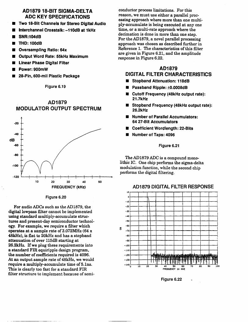
AD187918-BIT SIGMA-DELTA ADC KEY SPECIFICATIONS
• Two 18-Bit Channels for Stereo Digital Audio
• Interchannel Crosstalk: -110dB at 1kHz
• SNR:104dB
• THO: 100dB
• Oversampling Ratio: 64x
• Output Word Rate: 55kHz Maximum
• Linear Phase Digital Filter
• Power: 900mW
• 28-Pin, 600-mil Plastic Package
Figure 6.19
AD1879 MODULATOR OUTPUT SPECTRUM
-20
-40
dB -60
-80
-100
10 20 30 40
FREQUENCY (kHz)
Figure 6.20
For audioADCs such as theAD1879, the digitallowpass filter cannot be implemented using standard multiply-accumulate structures and present-day semiconductor technology. For example, we require a filter which operates at a sample rate of 3.072MHz (64 x 48kHz), is flat to 20kHz and has a stopband attenuation of over 115dB starting at 26.2kHz. If we plug these requirements into a standard Fffi equiripple design program, the number of coefficients required is 4096. At an output sample rate of 48kHz, we would require a multiply-accumulate time of 5.1ns. This is clearly too fast for a standard FIR filter structure to implement because of semi-
50
conductor process limitations. For this reason, we must use either a parallel processing approach where more than one multiply-accumulate is being executed at any one time, or a multi-rate approach where the decimation is done in more than one step. For the AD1879, a novel parallel processing approach was chosen as described further in Reference 1. The characteristics ofthis filter are given in Figure 6.21, and the amplitude response in Figure 6.22.
AD1879 DIGITAL FILTER CHARACTERISTICS • Stopband Attenuation: 118dB
• Passband Ripple: ±0.0008dB
• Cutoff Frequency (48kHz output rate): 21.7kHz
• Stopband Frequency (48kHz output rate): 26.2kHz
• Number of Parallel Accumulators: 64 27 ·Bit Accumu Ia tors
• Coefficient Wordlength: 22-Bits
• Number of Taps: 4096
Figure 6.21
The AD1879 ADC is a compound monolithic IC. One chip performs the sigma-delta modulation function, while the second chip performs the digital filtering.
AD1879 DIGITAL FILTER RESPONSE 10
·10 1\ ·20
-30
-•o -50
-60 cD 0
-70
-eo
-90
-100
-110
-120
-130 >liaJ - ~ ;~ •·m•" n~rr11r1 Rl"lllml I IIIII I' :T rr r 'I
-l•oo 10 20 30 •o !50 60 10 eo 90 soo FREQUENCY 1n KHZ
Figure 6.22

SIGMA-DELTA ADCs FOR Low FREQUENCY MEAsUREMENT APPLICATIONS
Applications such as industrial process control, weigh scales, temperature and pressure measurement instruments require ADCs which can digitize low frequency signals (usually less than 10Hz) to 16 bit or higher precision. In the past, this need was filled almost exclusively by integrating (or dual-slope) ADCs. Sigma-delta converters offer an attractive alternative. In addition to reduced cost and size, low frequency sigmadelta ADCs offer on-board digital filtering as well as system and self-calibration functions. Sampling rates allow processing of signals of up to 10Hz bandwidths, and power line frequency rejection of sigma-delta ADCs can be maintained over a much wider range of frequency variation than with traditional integrating ADCs. Power supply rejection of dual slope ADCs depends on the instantaneous line frequency variations since the sampling clock is synchronized to the line.
A functional block diagram of the AD770 1 monolithic 16 bit sigma-deltaADC is shown in Figure 6.23 and key specifications in Figure 6.24.
ADn01 BLOCK DIAGRAM
AVoo OY00 AVss DVss SC1 SC2
CLKIN CLKOUT MODE CS DRDY
Figure 6.23
The AD7701 contains a second-order sigma-delta modulator which samples the analog input signal at a 16kHz rate when the external clock frequency is 4.096MHz. The quantization noise is therefore spread over the bandwidth 0 to 8kHz. The device contains a 6-pole gaussian lowpass digital filter which has a cutoff frequency of 10Hz at the maximum clock rate. The 16kHz sampling rate therefore represents an oversam-
BPlUP
AD7701 LOW FREQUENCY MEASUREMENT
ADC KEY SPECIFICATIONS
• Monolithic 16-Bit ADC
• 0.0015o/o Linearity Error
• 4 kSPS Output Data Rate
• Programmable Low Pass Filter: 0.1Hz to 10Hz Corner Frequency
• On-Chip Self-Calibration Circuitry
• 0 to +2.5V or ±2.5V Input Range
• 40mW Power Dissipation
• 20J.1W Standby Mode
• Flexible Serial Interface
Figure 6.24
piing ratio of 800 with respect to the 10Hz cutoff frequency. The filter provides 55d.B of 60Hz rejection under these conditions. If the clock frequency is halved to give a 5Hz cutoff, 60Hz rejection is better than 90d.B. Power supply rejection is 70d.B in the 0.1 to 10Hz bandwidth, and PSRR at 60Hz exceeds 120d.B due to the digital filter. The frequency response of the digital filter at various clock rates is shown in Figure 6.25.
AD7701 DIGITAL FILTER RESPONSE
20
0
-20
-40 Ill Ill "C -60 I
~ -80 CJ
-100
-120
-140
-160 1
-~ ......... ""'-..... ~fcLK=4MHz ,._, ' ' I" ' ' fcLK•2MHz ' ~ I" I\.
" 1\..
"' '"-~,
fcLK = 1MHz"'
10
FREQUENCY - Hz
Figure 6.25
""I\ ~
' 100
The long settling time of the internal digital filter (shown in Figure 6.26) in the AD7701limits its use in multiplexed applications where channels are switched and converted sequentially at high rates. Switching between channels which may have different signal levels can cause a step change in the input. The AD7701is primarily intended for distributed converter systems using one ADC per channel. Multiplexing is possible, provided that sufficient settling time is allowed before data for the new channel is
AD7701 DIGITAL FILTER STEP RESPONSE
100 LU ::> ~
~ 80 ~ c z y: 60 II. 0 ... ffi 40 (.) a: LU
L_ 1/
J I a.. 20
LL 0 0 40 80
TIME-ms
Figure 6.26
120
accessed. The gaussian response worst case settling time to ±0.0007% ( ±0.5LSB) is 125ms with a 4.096MHz master clock frequency.
The AD7701 offers two calibration modes using the on-chip calibration microcontroller and SRAM. In the self-calibration mode, zero-scale is calibrated against the analog ground pin (AGND), andfullscale is calibrated against v ref pin. In the system-calibration mode, the AD7701 calibrates its zero and fullscale to voltages present on the analog input pin in two sequential steps, thereby allowing system offests and/or gain errors to be nulled out.
The AD7703 sigma-delta ADC has a similar architecture to the AD7701, but achieves 20 bits of resolution with 0.0003% linearity error. Key specifications for the AD7703 are summarized in Figure 6.27.
AD7703
160
LOW FREQUENCY MEASUREMENT ADC KEY SPECIFICATIONS
• Monolithic 22-Bit ADC
• 0.0003% Linearity Error
• 4 kSPS Output Data Rate
• Programmable Low Pass Filter: 0.1 Hz to 1OHz Corner Frequency
• On-Chip Self-Calibration Circuitry
• 0 to +2.5V or ±2.5V Input Range
• 40mW Power Dissipation
• 20JJ.W Standby Mode
• Flexible Serial Interface
Figure 6.27
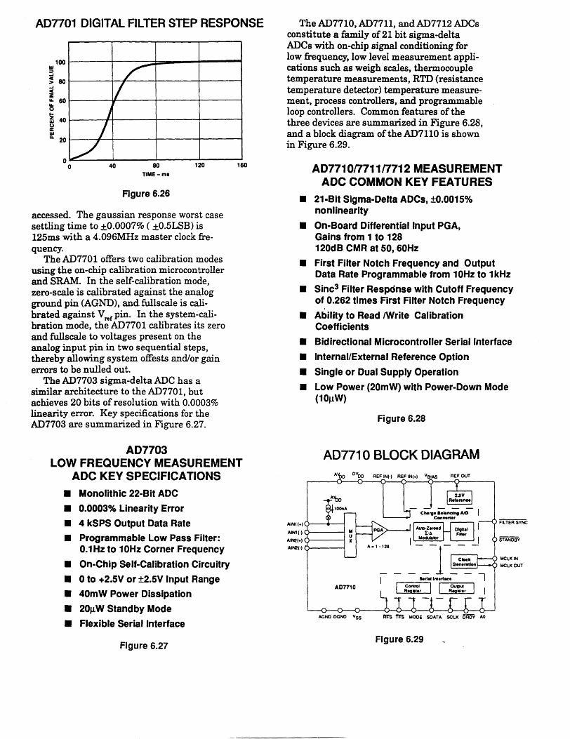
The AD7710, AD7711, and AD7712 ADCs constitute a family of 21 bit sigma-delta ADCs with on-chip signal conditioning for low frequency, low level measurement applications such as weigh scales, thermocouple temperature measurements, RTD (resistance temperature detector) temperature measurement, process controllers, and programmable loop controllers. Common features of the three devices are summarized in Figure 6.28, and a block diagram of the AD7110 is shown in Figure 6.29.
AD771 0/7711/7712 MEASUREMENT ADC COMMON KEY FEATURES
• 21-Bit Sigma-Delta ADCs, ±0.0015% nonlinearity
• On-Board Differential Input PGA, Gains from 1 to 128 120dB CMR at 50, 60Hz
• First Filter Notch Frequency and Output Data Rate Programmable from 1OHz to 1kHz
• Sinc3 Filter Respdnse with Cutoff Frequency of 0.262 times First Filter Notch Frequency
• Ability to Read /Write Calibration Coefficients
• Bidirectional Microcontroller Serial Interface
• Internal/External Reference Option
• Single or Dual Supply Operation
• Low Power (20mW) with Power-Down Mode (10J.LW)
Figure 6.28
AD771 0 BLOCK DIAGRAM A'bo OVOO REF IN(·) REF IN(+) VBIAS REF OUT
AIN1 (+) l>----+----1 AIN1(·) D-------1 AIN2(+) D-------1 AIN2(-) (}------1
AD7710
AGNO OGNO Vss An m MODE SOATA SCLK OROY AO
Figure 6.29
MCLK IN
MCLKOUT

AD771 0/7711 m12 DIGITAL FILTER RESPONSE
o ffi: ·----r ·1···"'-· - ..... ··~-·······
-r --r 1 r---· -r rr' I -- i\ ,.,.. i
~ -l-._L \1 1 \ /f\ }'"to\. ...l :E. _
100 i i 1 \I I \ I \ I ! \ I
~ -L 1 ! \1
(!) i i +-- -· -r-r- ! i :
--,- i ·-r---200 ·-·- i.-+·-'--1~-'---t---'--+---4--~-"--·
i i
0 20 40 60
FREQUENCY (Hz)
Figure 6.30
An on-board differential input PGA (gain = 1 to 128) enables the user to control fullscale voltage and voltage resolution. The effects of temperature drift are minimized by on-chip self-calibration which removes zero scale and fullscale errors. The internal digital filter has a (sin x/x)3 response, and 12 bits of data programmed into the control register determine the filter cutoff frequency, the position of the firstnotch of the filter, and the data rate. In association with the gain selection, it also determines the useful resolution of the device. The first notch frequency (which is also the output data rate) can be programmed from 10Hz to 1kHz. The corresponding -3d.B frequency is equal to 0.262 times the first notch frequency. Figure 6.30 shows the filter frequency response for a cutofffrequency of2.62Hz which corresponds to a first filter notch frequency of 10Hz. The filter response provides greater than 100dB of 50Hz and 60Hz common mode rejection.
Key device-specific features for the three devices are given in Figures 6.31.
AD771 on111 n112 DEVICE-SPECIFIC FEATURES
AD7710: • Two-Channel Differential Low-Level
PGA Input
ADn11: • Single-Channel Differential Low-Level
PGA Input • RTD (Resistance Temperature Detector)
Excitation Current Sources
ADn12: • Single-Channel Differential Low-Level
PGA Input • High-Level Analog Input
Figure 6.31
SIGMA· DELTA DACs
Sigma-delta D/A conversion can generally be thought of as the AID conversion process in the reverse order, where all the basic functions of the digital filter and sigma-delta modulator previously discussed are the same. Sigma-delta DACs offer essentially the same advantages as sigma-delta ADCs. Because of the large oversampling ratio, the requirements on the antialiasing reconstruction filter are greatly relaxed. However, care must be taken to make sure the high frequency noise components contained in the one-bit DAC output are filtered sufficiently. If a higher order filter is required to reduce this noise, then some of the advantages of the sigma-delta DAC architecture are lost.
Accurate, low-cost, high resolution laser wafer trimmed DACs are readily available, and for this reason there has been less pressure to fully exploit sigma-delta DACs at the component level. The real incentive for developing the sigma-delta DAC technology is because it is the ideal architecture for mixed-signal ICs which require the chip-level integration of the ADC, DAC, and DSP functions.
SIGMA-DELTA DAC CONCEPTS
• Basically a Sigma-Delta ADC in Reverse
• Low-Cost, High Resolution R/2R DACs Proliferate at the Component Level with Oversampling Capability
• Sigma-Delta DACs Ideal for Chip-Level Integration with ADC and DSP Functions
• Antialiasing Filter Must Remove High Frequency Noise
Figure 6.32
The tradi tiona! approach to achieving high performance and wide dynamic range using RI2R-based DACs is shown in Figure 6.33. Due to the binary nature of the internal DAC switches, code-dependent transients, or glitches, typically produce some amount of harmonic distortion in the output spectrum. As discussed previously in the DAC section of this seminar, a technique called segmentation can greatly minimize these effects. For the ultimate in spectral purity, the remaining glitches can be removed with a sample-and-holfl circuit which holds the DAC output voltage for the duration of the glitch. This technique can eliminate the code-dependent glitches (hence
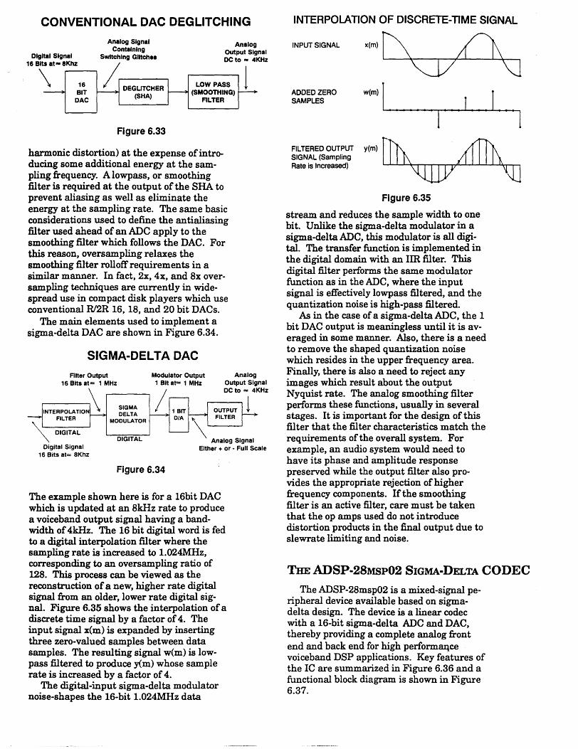
CONVENTIONAL DAC DEGLITCHING
Digital Signal 16 Bits at• 8Khz
Analog Output Signal DC to • 4KHz
\ 16 BIT
DAC
LOW PASS 1 (SMOOTHING)
FILTER
Figure 6.33
harmonic distortion) at the expense of introducing some additional energy at the sampling frequency. A lowpass, or smoothing filter is required at the output of the SHA to prevent aliasing as well as eliminate the energy at the sampling rate. The same basic considerations used to define the antialiasing filter used ahead of an ADC apply to the smoothing filter which follows the DAC. For this reason, oversampling relaxes the smoothing filter roll off requirements in a similar manner. In fact, 2x, 4x, and 8x oversampling techniques are currently in widespread use in compact disk players which use conventional R/2R 16, 18, and 20 bit DACs.
The main elements used to implement a sigma-delta DAC are shown in Figure 6.34.
SIGMA-DELTA DAC
Alter Output 16 Bits at= 1 MHZ
INTERPOlATIOJ\ FILTER
Modulator Output 1 Bit at= 1 MHz
/,.n Analog
Output Signal DC to= 4KHz
DIGITAL
SIGMA DELTA
MODULATOR
1
Digital Signal 16 Bits at= 8Khz
DIGITAL Analog Signal Either + or - Full Scale
Figure 6.34
The example shown here is for a 16bit DAC which is updated at an 8kHz rate to produce a voiceband output signal having a bandwidth of 4kHz. The 16 bit digital word is fed to a digital interpolation filter where the sampling rate is increased to 1.024MHz, corresponding to an oversampling ratio of 128. This process can be viewed as the reconstruction of a new, higher rate digital signal from an older, lower rate digital signal. Figure 6.35 shows the interpolation of a discrete time signal by a factor of 4. The input signal x(m) is expanded by inserting three zero-valued samples between data samples. The resulting signal w(m) is lowpass filtered to produce y(m) whose sample rate is increased by a factor of 4.
The digital-input sigma-delta modulator noise-shapes the 16-bit 1.024MHz data
INTERPOLATION OF DISCRETE-TIME SIGNAL
INPUT SIGNAL
ADDED ZERO SAMPLES
Fll TEA ED OUTPUT SIGNAL (Sampling Rate is Increased)
x(m)f\ £1 ~ \j
w(m)] ~-----r-~-· . ...L.I -..1.--
y(m) Ul\ A1TII\ \Q]Y~
Figure 6.35
stream and reduces the sample width to one bit. Unlike the sigma-delta modulator in a sigma-delta ADC, this modulator is all digital. The transfer function is implemented in the digital domain with an Iffi filter. This digital filter performs the same modulator function as in the ADC, where the input signal is effectively lowpass filtered, and the quantization noise is high-pass filtered.
As in the case of a sigma-deltaADC the 1 bit DAC output is meaningless until it is averaged in some manner. Also, there is a need to remove the shaped quantization noise which resides in the upper frequency area. Finally, there is also a need to reject any images which result about the output Nyquist rate. The analog smoothing filter performs these functions, usually in several stages. It is important for the design of this filter that the filter characteristics match the requirements of the overall system. For example, an audio system would need to have its phase and amplitude response preserved while the output filter also provides the appropriate rejection of higher frequency components. If the smoothing filter is an active filter, care must be taken that the op amps used do not introduce distortion products in the final output due to slewrate limiting and noise.
THE ADSP-28MSP02 SIGMA-DELTA CODEC
. The ADS~-28msp02 is a mixed-signal penpheral deVIce available based on sigmadelta design. The device is a linear codec with a 16-bit sigma-delta ADC and DAC, thereby providing a complete analog front end and back end for high perform8.J.lce voiceband DSP applications. Key features of the IC are summarized in Figure 6.36 and a functional block diagram is shown in Figure 6.37.

KEY FEATURES OF THE ADSP-28msp02 SIGMA-DELTA CODEC
• 16-Bit Sigma-Delta ADC
• 16-Bit Sigma-Delta DAC
• On-Chip Antialiasing and Smoothing Filters
• SkSPS Sampling Rate, 128x Oversampling Ratio
• On-Chip Voltage Reference
• 65dB SNR and THO
• Easy Interface to DSP ChIps
• 24-Pin DIP/SOIC Package
• Single +5V Supply, 100mV Power Dissipation
• Ideal for Voiceband Applications
Figure 6.36
Compared to traditional m-law and A-law codecs, the ADSP-28msp02's linear coded ADC and DAC maintain wide dynamic range throughout the transfer function. An effective sampling rate of BkSPS coupled with 65d.B SNR and THD performance make the device attractive in many telecommunications applications such as digital cellular telephones. The part is packaged in a 24-pin DIP/SOIC package ensuring a highly integrated and compact solution to voiceband analog processing requirements. The ADSP-28msp02 easily interfaces to the ADSP-2101, ADSP-2105, ADSP-2111, MC56001 and TMS320C25 DSP processors via its serial 110 port; the serial port (SPORT) is used to transmit and receive data or control information to and from the device.
The encoder side of the ADSP-28msp02 consists of two selectable analog input amplifiers and a sigma-delta ADC. The gain of the input amplifiers can be adjusted with the use of external resistors from -12dB to +26dB. An optional 20dB preamplifier can be inserted before the modulator. The preamplifier and the multiplexer are configured by bits in the control register. The sigma-delta ADC consists of a sigma-delta modulator, an antialiasing decimation filter, and a digital high pass filter. The modulator noise-shapes the signal and produces 1-bit samples at a 1.024MHz rate. This bit stream, represent• ing the analog input, is fed to an antialiasing decimation filter which consists of two lowpass filter stages. The first stage reduces the sampling rate to 40kHz and increases the sample width to 16 bits; the second further reduces the sampling rate to BkSPS. Each resulting sam pie is then loaded into the SPORT for transmission.
The decoder consists of a sigma-delta DAC and a differential output amplifier. The DAC reads 16-bit samples at an 8kHz rate from the SPORT. The samples are low- and highpass filtered by the digital anti-imaging and high pass filters. The anti-imaging filter interpolates the sampling rate in two stages, first to 40kHz, and then to 1.024MHz. The resulting 16-bit samples are processed by the digital sigma-delta modulator which reduces the sample width to 1 bit. This bit stream is fed to an analog smoothing filter which converts the data to an analog voltage. The gain of the smoothing filter can be adjusted via the control register from -15dB to +6d.B is 3dB steps.
ADSP-28msp02 BLOCK DIAGRAM
Figure 6.37
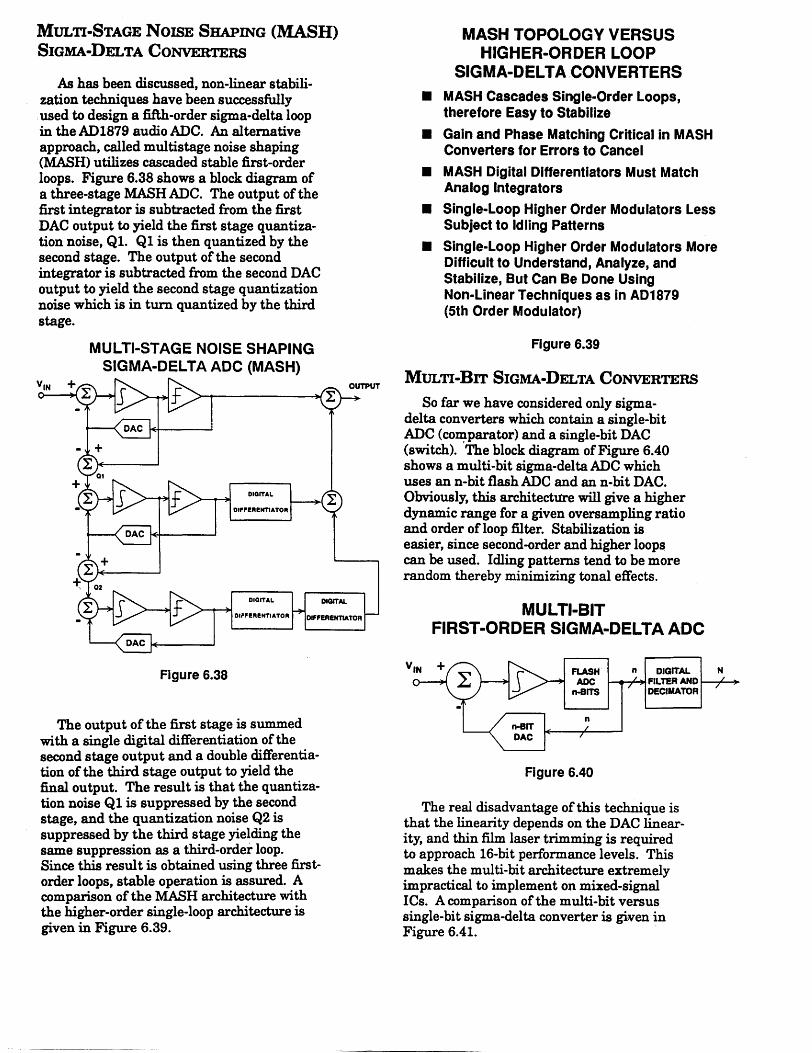
MULTI-STAGE NoiSE SHAPING (MASH)
SIGMA-DELTA CONVERTERS
As has been discussed, non-linear stabilization techniques have been successfully used to design a fifth-order sigma-delta loop in the AD1879 audio ADC. An alternative approach, called multistage noise shaping (MASH) utilizes cascaded stable first-order loops. Figure 6.38 shows a block diagram of a three-stage MASH ADC. The output of the first integrator is subtracted from the first DAC output to yield the first stage quantization noise, Ql. Ql is then quantized by the second stage. The output of the second integrator is subtracted from the second DAC output to yield the second stage quantization noise which is in tum quantized by the third stage.
MULTI-STAGE NOISE SHAPING SIGMA-DELTA ADC (MASH)
Figure 6.38
The output of the first stage is summed with a single digital differentiation of the second stage output and a double differentiation of the third stage output to yield the final output. The result is that the quantization noise Ql is suppressed by the second stage, and the quantization noise Q2 is suppressed by the third stage yielding the same suppression as a third-order loop. Since this result is obtained using three firstorder loops, stable operation is assured. A comparison of the MASH architecture with the higher-order single-loop architecture is given in Figure 6.39.
MASH TOPOLOGY VERSUS HIGHER-ORDER LOOP
SIGMA-DEL TA~CONVERTERS
• MASH Cascades Single-Order Loops, therefore Easy to Stabilize
• Gain and Phase Matching Critical in MASH Converters for Errors to Cancel
• MASH Digital Differentiators Must Match Analog Integrators
• Single-Loop Higher Order Modulators Less Subject to Idling Patterns
• Single-Loop Higher Order Modulators More Difficult to Understand, Analyze, and Stabilize, But Can Be Done Using Non-Linear Techniques as in AD1879 (5th Order Modulator)
Figure 6.39
MULTI-BIT SIGMA-DELTA CONVERTERS
So far we have considered only sigmadelta converters which contain a single-bit ADC (co~parator) and a single-bit DAC (switch). The block diagram of Figure 6.40 shows a multi-bit sigma-deltaADC which uses an n-bit flash ADC and an n-bit DAC. Obviously, this architecture will give a higher dynamic range for a given oversampling ratio and order of loop filter. Stabilization is easier, since second-order and higher loops can be used. Idling patterns tend to be more random thereby minimizing tonal effects.
MULTI-BIT FIRST -ORDER SIGMA-DELTA ADC
Figure 6.40
n DIGITAL N FILTER AND DECIMA TOR
The real disadvantage of this technique is that the linearity depends on the DAC linearity, and thin film laser trimming is required to approach 16-bit performance levels. This makes the multi-bit architecture extremely impractical to implement on mixed-signal ICs. A comparison of the multi-bit versus single-bit sigma-delta converter is given in Figure 6.41. ·

MULTI-BIT VERSUS SINGLE-BIT
SIGMA DELTA CONVERTERS Multi-Bit: • Higher Dynamic Range for Given
Oversampling Ratio and Loop Filter Order
• Higher Order Systems Easier to Stabilize
• Fewer Tonal Effects due to Idling Patterns
• Linearity Depends on DAC
• Thin Film Laser Trimming Required
Single-Bit: • Perfect Linearity, no Strict Matching
Requirements
• No Laser Trimming Required
• Perfect Topology for Mixed-Signal VLSI
• Non-Linear Techniques Required to Stabilize Higher Order Loops (AD1879)
Figure 6.41
SIGMA-DELTA SUMMARY
Although the concepts used in sigma-delta converters are not new by any means, their recent proliferation has been primarily driven by the need for converters which are compatible with mixed-signal VLSI chips. The sigma-delta architecture is ideal for converters for measurement, voiceband, and audio applications. Further exploration of various sigma-delta circuit topologies combined with the development of new processes is sure to push the maximum dynamic range and sampling rates even higher.
It is clear that the sigma-delta converter is not the answer to all data acquisition requirements at the present time. Upper sampling frequency is limited, thereby excluding video applications, multiplexing inputs is difficult due to the settling time of the internal digital filter, and out-of-range signals may cause saturation of the internal modulators.
On the other hand, the inherently good linearity performance without the need for laser trimming, the relaxation of antialiasing and anti-imaging filter requirements due to oversampling, and the basic sampling nature of the architecture without the need for a SHA will keep sigma-delta development moving at a rapid pace as mixed-signal ICs proliferate.
SIGMA-DELTA SUMMARY
• Inherently Excellent Linearity
• Ideal for Mixed-SignaiiC Processes, no Trimming
• No SHA Required
• Upper Sampling Rate Currently Limits Applications to Measurement, Voiceband, and Audio
• Out-of-Range Signals May Cause Modulator Saturation
• Analog Multiplexing Applications Limited by Internal Filter: Use one Sigma-Delta ADC per Channel!
Figure 6.42
I :-----·-------· REFERENCES
1. J. Dattorro, A Charpentier, D. Andreas, The Implementation of a OneStage Multirate 64:1 Fffi Decimator for use in One-Bit Sigma-Delta AID Applications, AES 7th International Conference, May 1989.
2. W.L. Lee and C. G. Sodini, A 1bpology for Higher-Order Interpolative Coders, ISCAS PROC. 1987.
3. P.F. Ferguson, Jr., A Ganesan and R. W. Adams, One Bit Higher Order Sigma-Delta AID Converters, ISCAS PROC. 1990, Vol. 2, pp. 890-893.
4. R. Koch, B. Heise, F. Eckbauer, E. Engelhardt, J. Fisher, and F. Parzefall, A 12-bit Sigma-Delta Analog-to-Digital Converter with a 15MHz Clock Rate, IEEE Journal of Solid-State Circuits, Vol. SC-21, No. 6, December
"1986.
5. Wai Laing Lee, A Novel Higher Order Interpolative Modulator 1bpology for High Resolution Oversampling AID Converters, MIT Masters Thesis, June 1987.
6. D. R. Weiland, B. P. Del Signore and E. J. Swanson, A Stereo 16-Bit Delta-Sigma AID Converter for Digital Audio, J. Audio Engineering Society, Vol. 37, No.6, June 1989, pp. 476-485.
7. R. W. Adams, Design and Implementation of an Audio 18-Bit Analogto-Digital Converter Using Oversampling Techniques, J. Audio Engineering Society, Vol. 34, March 1986, pp. 153-166.
8 B. Boser and Bruce Wooley, The Design of Sigma-Delta Modulation Analog-to-Digital Converters, IEEE Journal of Solid-State Circuits, Vol. 23, No.6, December 1988, pp. 1298-1308.
9. Y. Matsuya, et. al., A 16-Bit Oversampling AID Conversion Technology Using 1iiple-Integration Noise Shaping, IEEE Journal of Solid-State Circuits, Vol. SC-22, No.6, December 1987, pp. 921-929.
10. Y. Matsuya, et. al., A 17-Bit Oversampling D/A Conversion Technology Using Multistage Noise Shaping, IEEE Journal of Solid-State Circuits, Vol. 24, No. 4, August 1989, pp. 969-975.
11. P. Ferguson, Jr., A Ganesan, R. Adams, et. al., An 18-Bit 20-kHz Dual Sigma-Delta AID Converter, ISSCC Digest of Thchnical Papers, February 1991.
12. Steven Harris, The Effects of Sampling Clock Jitter on Nyquist Sampling Analog-to-Digital Converters and on Oversampling Delta Sigma ADCs, Audio Engineering Society Reprint 2844 (F-4), October, 1989.