Embed Size (px)
Citation preview

Lecture 400 – Oversampling ADCs – Part II (3/29/10) Page 400-1
CMOS Analog Circuit Design © P.E. Allen - 2010
LECTURE 400 – OVERSAMPLING ADCS – PART IILECTURE ORGANIZATION
Outline• Implementation of modulators• Decimation and filtering• Bandpass modulators• Digital-analog oversampling converters• SummaryCMOS Analog Circuit Design, 2nd Edition ReferencePages 705-715
Lecture 400 – Oversampling ADCs – Part II (3/29/10) Page 400-2
CMOS Analog Circuit Design © P.E. Allen - 2010
IMPLEMENTATION OF MODULATORS Modulators – The Analog Part of the Oversampling ADC
Most of today’s delta-sigma modulators use fully differential switched capacitor circuits.Advantages are:• Doubles the signal swing and increases the dynamic range by 6dB• Common-mode signals that may couple to the signal through the supply lines and
substrate are canceled• Charge injected by the switches are canceled to a first-orderExample:
First integratordissipates the mostpower and requires themost accuracy.
Fig.10.9-24
YB
Y
-
+ 0.5z-11 - z-1
-
+ 0.5z-11 - z-1
++X Y
Q1
+
-
VRef+
φ1dφ1d
Y YB
φ2φ2
VRef+ VRef
-
VRef-
2C
2C
C
Cφ1dφ1d
YYB
VRef+
Y YB
VRef-
φ1
φ1
VRef+ VRef
-
YYB
+
-φ2φ2
2C
2C
C
C
φ1
φ1
φ1

Lecture 400 – Oversampling ADCs – Part II (3/29/10) Page 400-3
CMOS Analog Circuit Design © P.E. Allen - 2010
1.5V, 1mW, 98db Analog-Digital Converter†
a1z - 1Σ
b1
Σ Σa2
z - 1
b2
a3z - 1
a4z - 1
Σ
1-bitA/D
1-bitD/A
α E
y4Y
y3y2y1
X
Fig. 10.10-06
where a1 = 1/3, a2 = 3/25, a3 = 1/10, a4 = 1/10, b1= 6/5, b2= 1 and = 1/6
Advantages: • The modulator combines the advantages of both DFB and DFF type modulators:
Only four op amps are required. The 1st integrator’s output swing is between ±VREFfor large input signal amplitudes (0.6VREF), even if the integrator gain is large (0.5).
• A local resonator is formed by the feedback around the last two integrators to furthersuppress the quantization noise.
• The modulator is fully pipelined for fast settling.
† A.L. Coban and P.E. Allen, “A 1.5V, 1mW Audio Modulator with 98dB Dynamic Range, “Proc. of 1999 Int. Solid-State Circuits Conf., Feb.
1999, pp. 50-51.
Lecture 400 – Oversampling ADCs – Part II (3/29/10) Page 400-4
CMOS Analog Circuit Design © P.E. Allen - 2010
1.5V, 1mW, 98dB Analog-Digital Converter - ContinuedIntegrator power dissipation vs. integrator gain
DR = 98 dBBW = 20 kHzCs = 5 pF0.5 μm CMOS

Lecture 400 – Oversampling ADCs – Part II (3/29/10) Page 400-5
CMOS Analog Circuit Design © P.E. Allen - 2010
1.5V, 1mW, 98db Analog-Digital Converter - ContinuedModulator power dissipation vs. oversampling ratio
SuppyVoltage (V)
DR = 98 dBBW = 20 kHzIntegrator gain = 1/30.5μm CMOS
OSR = 64
OSR = 32
OSR = 16 OSR = 8
Lecture 400 – Oversampling ADCs – Part II (3/29/10) Page 400-6
CMOS Analog Circuit Design © P.E. Allen - 2010
1.5V, 1mW, 98dB Analog-Digital Converter - ContinuedCircuit Implementation:
Capacitor ValuesCapacitor Integrator 1 Integrator 2 Integrator 3 Integrator 4
Cs 5.00pF 0.15pF 0.30pF 0.10pFCi 15.00pF 1.25pF 3.00pF 1.00pFCa - - 0.05pF -
Cb1 - - - 0.12pFCb2 - - - 0.10pF Fig.10.9-25
1
1d
2
2d

Lecture 400 – Oversampling ADCs – Part II (3/29/10) Page 400-7
CMOS Analog Circuit Design © P.E. Allen - 2010
1.5V, 1mW, 98dB Analog-Digital Converter - ContinuedMicrophotograph of the modulator.
Lecture 400 – Oversampling ADCs – Part II (3/29/10) Page 400-8
CMOS Analog Circuit Design © P.E. Allen - 2010
1.5V, 1mW, 98dB Analog-Digital Converter - ContinuedMeasured SNR and SNDR versus input level of the modulator.

Lecture 400 – Oversampling ADCs – Part II (3/29/10) Page 400-9
CMOS Analog Circuit Design © P.E. Allen - 2010
1.5V, 1mW, 98dB Analog-Digital Converter - ContinuedMeasured baseband spectrum for a -7.5dBr 1kHz input.
Lecture 400 – Oversampling ADCs – Part II (3/29/10) Page 400-10
CMOS Analog Circuit Design © P.E. Allen - 2010
1.5V, 1mW, 98dB Analog-Digital Converter - ContinuedMeasured baseband spectrum for a -80dBr 1kHz input.
-80 dBr, 1 kHz signalVREF = 1.5 V (diff.)2048-point FFT
frequency, (kHz)

Lecture 400 – Oversampling ADCs – Part II (3/29/10) Page 400-11
CMOS Analog Circuit Design © P.E. Allen - 2010
1.5V, 1mW, 98dB Analog-Digital Converter - ContinuedMeasured 4th-Order Modulator Characteristics:
Table 5.4
Measured fourth-order delta-sigma modulator characteristics
Technology : 0.5 μm triple-metal single-poly n-well CMOS process
Supply voltage 1.5 V
Die area 1.02 mm x 0.52 mm
Supply current 660 μA
analog part 630 μA
digital part 30 μA
Reference voltage 0.75V
Clock frequency 2.8224MHz
Oversampling ratio 64
Signal bandwidth 20kHz
Peak SNR 89 dB
Peak SNDR 87 dB
Peak S/D 101dB
HD @ -5dBv 2kHz input -105dBv
DR 98 dB3
Lecture 400 – Oversampling ADCs – Part II (3/29/10) Page 400-12
CMOS Analog Circuit Design © P.E. Allen - 2010
DECIMATION AND FILTERINGDelta-Sigma ADC Block DiagramThe decimator and filterare implemented digitallyand consume most of thearea and the power.Function of the decimatorand filter are;
1.) To attenuate thequantization noise above the baseband
2.) Bandlimit the input signal3.) Suppress out-of-band spurious signals and circuit noise
Most of the ADC applications demand decimation filters with linear phasecharacteristics leading to the use of finite impulse response (FIR) filters.FIR filters:
For a specified ripple and attenuation,
Number of filter coefficients fsft
where fs is the input rate to the filter (clock frequency of the quantizer) and ft is thetransition bandwidth.
Fig.10.9-07
ΔΣ Modulator(Analog)
Decimator(Digital)
Lowpass Filter(Digital)
fS fD<fS
AnalogInputx(t)
fB 2fB DigitalPCM

Lecture 400 – Oversampling ADCs – Part II (3/29/10) Page 400-13
CMOS Analog Circuit Design © P.E. Allen - 2010
A Multi-Stage Decimation FilterTo reduce the number of stages, the decimation filters are implemented in several stages.Typical multi-stage decimation filter:
Fig.10.9-26
L+1-th order
fs fs/D 2fN fN
First-halfband filter
Second-halfband filter
fN
Droopcorrection
1.) For modulators with (1-z-1)L noise shaping comb filters are very efficient.• Comb filters are suitable for reducing the sampling rate to four times the Nyquist
rate.• Designed to supress the quantization noise that would otherwise alias into the
signal band upon sampling at an intermediate rate of fs1.
2.) The remaining filtering is performed by in stages by FIR or IIR filters.• Supresses out-of-band components of the signal
3.) Droop correction - may be required depending upon the ADC specifications
Lecture 400 – Oversampling ADCs – Part II (3/29/10) Page 400-14
CMOS Analog Circuit Design © P.E. Allen - 2010
Comb FiltersA comb filter that computes a running average of the last D input samples is given as
y[n] = 1D
i = 0
D - 1
x[n-i]
where D is the decimation factor given as
D = fsfs1
The corresponding z-domain expression is,
HD(z) = i = 1
D
z-i = 1D
1 - z-D
1 - z-1
The frequency response is obtained by evaluating HD(z) for z = ej2 fTs,
HD(f) = 1D
sin fDTssin fTs
e-j2 fTs/D
where Ts is the input sampling period (=1/fs). Note that the phase response is linear.
For an L-th order modulator with a noise shaping function of (1-z-1)L, the requirednumber of comb filter stages is L+1. The magnitude of such a filter is,
|HD(f)| = 1D
sin fDTssin fTs
K

Lecture 400 – Oversampling ADCs – Part II (3/29/10) Page 400-15
CMOS Analog Circuit Design © P.E. Allen - 2010
Magnitude Response of a Cascaded Comb FilterK = 1,2 and 3
Fig.10.9-27
-100
-80
-60
-40
-20
0
Frequency
K = 1
K= 2
0 fb4 fsD
3 fsD
2 fsD
fsD
K = 3
|HD
(f)|
dB
Lecture 400 – Oversampling ADCs – Part II (3/29/10) Page 400-16
CMOS Analog Circuit Design © P.E. Allen - 2010
Implementation of a Cascaded Comb FilterImplementation:
Fig.10.9-28
-
+z-1
-
+z-1
-
+z-1
fs/D
K = L +1 Integrators
Numerator Section
z-1
+
-z-1
+
-z-1
+
-
X
Y
K = L +1 Differentiators
Denominator Section
Comments:1.) The L+1 integrators operating at the sampling frequency, fs, realize the denominator
of HD(z).2.) The L+1 differentiators operating at the output rate of fs1 (= fs/D) realize the
numerator of HD(z).
3.) Placing the integrator delays in the feedforward path reduces the critical path fromL+1 adder delays to a single adder delay.
Lecture 400 – Oversampling ADCs – Part II (3/29/10) Page 400-17
CMOS Analog Circuit Design © P.E. Allen - 2010
Implementation of Digital Filters†
Digital filter structures:
Fig.10.9-29
x(n) h(0) y(n)
Input Output
z-1h(1)
z-1h(2)
z-1h(3)
z-1h(N-1)
x(n)h(0)y(n)
InputOutput
z-1h(1)
z-1h(2)
z-1h(3)
z-1h(N-1)
Direct-form structure for an FIR digital filter.
Transposed direct-form FIR filter structure.
† S.R. Norsworthy, R. Schreier, and G.C. Temes, Delta-Sigma Data Converters-Theory, Design, and Simulation, IEEE Press, NY, Chapter 13, 1997.
Lecture 400 – Oversampling ADCs – Part II (3/29/10) Page 400-18
CMOS Analog Circuit Design © P.E. Allen - 2010
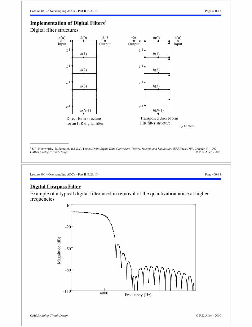
Digital Lowpass FilterExample of a typical digital filter used in removal of the quantization noise at higherfrequencies
-110
-80
-50
-20
10
4000 Frequency (Hz)
Mag
nitu
de (
dB)

Lecture 400 – Oversampling ADCs – Part II (3/29/10) Page 400-19
CMOS Analog Circuit Design © P.E. Allen - 2010
Illustration of the Delta-Sigma ADC in Time and Frequency Domain
MODULATOR
DECIMATORLOW-PASS
FILTERanalog input
fDfS
2fB
digital PCM
fB
TimeTime
Frequency FrequencyFrequency
Lecture 400 – Oversampling ADCs – Part II (3/29/10) Page 400-20
CMOS Analog Circuit Design © P.E. Allen - 2010
BANDPASS DELTA-SIGMA MODULATORSBandpass ModulatorsBlock diagram of a bandpass modulator:
Components:• Resonator - a bandpass filter of order
2N, N= 1, 2,....• Coarse quantizer (1 bit or multi-bit)The noise-shaping of the bandpass oversampled ADC has the following interestingcharacteristics:
Center frequency = fs ·(2N-1)/4
Bandwidth = BW = fs /M
Illustration of the Frequency Spectrum(N=1):
Application of the bandpass ADC isfor systems with narrowband signals (IF frequencies)
Fig.10.9-27A
-
+Resonator A/D
D/A
x
u
v y
Quantizer
fS
Frequency3fs4
fs4
fs
BW BW
dB
Attenuation
0Fig. 11-32

Lecture 400 – Oversampling ADCs – Part II (3/29/10) Page 400-21
CMOS Analog Circuit Design © P.E. Allen - 2010
A First-Order Bandpass ModulatorBandpass Resonator:
V(z) = z-1 [X(z) - z-1V(z)] = z-1X(z) - z-2V(z)
V(z) (1+z-2) = z-1X(z)V(z)X(z) =
z-1
1+z-2
Modulator:
Y(z) = Q(z) + [X(z) - Y(z)] z-1
1+z-2
Y(z) = 1+z-2
1+ z-1-z-2Q(z) +
z-1
1+ z-1-z-2X(z)
NTFQ (z) = 1+z-2
1+ z-1-z-2
The NTFQ (z) has two zeros on the j axis.
z-1
z-1
ΣX(z) V(z)+
-
Fig. 10.9-27C
Fig.10.9-27B
-
+ z-1 +X(z)
Q(z)
Y(z)
1+z-2
Lecture 400 – Oversampling ADCs – Part II (3/29/10) Page 400-22
CMOS Analog Circuit Design © P.E. Allen - 2010
Resonator DesignResonators can be designed by applying a lowpass to bandpass transform as follows:
z-1ΣX(z) V(z)+
+
Fig. 10.9-27D
z-2ΣX(z) V(z)+
+
Replace z-1 by -z-2
1 - z-1z-1
1 + z-2-z-2
Result:• Simple way to design the resonator• Inherits the stability of a lowpass modulator• Center frequency located at fs/4

Lecture 400 – Oversampling ADCs – Part II (3/29/10) Page 400-23
CMOS Analog Circuit Design © P.E. Allen - 2010
Fourth-Order Bandpass ModulatorBlock diagram:
ΣX(z) Y(z)+
-
Fig. 10.9-27E
1 + z-2z-2
0.5 Σ+
+ 1 + z-2z-2
0.5
Comments:• Designed by applying a lowpass to bandpass transform to a second-order lowpass
modulator• The stabilty and SNR characteristics are the same as those of a second-order lowpass
modulator• The z-domain output is given as,
Y(z) = z-4X(z) + (1+z-2)2Q(z)• The zeros are located at z = ±j which corresponds to notches at fs/4.
Lecture 400 – Oversampling ADCs – Part II (3/29/10) Page 400-24
CMOS Analog Circuit Design © P.E. Allen - 2010
Resonator Circuit Implementation
Block diagram of z-2/(1+z-2):
z-1 z-1ΣX(z) V(z)+
+
Fig. 10.9-27FFully differential switch-capacitor implementation:

Lecture 400 – Oversampling ADCs – Part II (3/29/10) Page 400-25
CMOS Analog Circuit Design © P.E. Allen - 2010
Power Spectral Density of the Previous Fourth-Order Bandpass ModulatorSimulated result:
Lecture 400 – Oversampling ADCs – Part II (3/29/10) Page 400-26
CMOS Analog Circuit Design © P.E. Allen - 2010
DELTA-SIGMA DIGITAL-TO-ANALOG CONVERTERSPrinciplesThe principles of oversampling and noise shaping are also widely used in theimplementation of DACs.Simplified block diagram of a delta-sigma DAC:
Digitaldelta-sigmamodulator
Interpolat-ion filter
Analoglowpass
filterDAC
N-bit
MfN
N-bit
fN
1-bit
MfN MfN
Input
Digital Section Analog Section
Output
Fig10.9-29
Operation:1.) A digital signal with N-bits with a data rate of fN is sampled at a higher rate of MfN by
means of an interpolator.2.) Interpolation is achieved by inserting “0”s between each input word with a rate of
MfN and then filtering with a lowpass filter.
3.) The MSB of the digital filter is applied to a DAC which is applied to an analoglowpass filter to achieve the analog output.

Lecture 400 – Oversampling ADCs – Part II (3/29/10) Page 400-27
CMOS Analog Circuit Design © P.E. Allen - 2010
Block Diagram of a DAC
AnalogOutput-
+Interpol-ation
DigitalFilter
Digital Code Conversion
0→100000000000000 =-11→011111111111111 = 1
VRef
-VRef
DigitalInput
fN
fS=MfNfS
fS
fS
AnalogLowpass
Filter
MSB
DAC
fS fS
Fig10.9-31
y(k)
Operation:1.) Interpolate a digital word at the conversion rate of the converter (f
N) up to the sample
frequency, fs.2.) The word length is then reduced to one bit with a digital sigma-delta modulator.3.) The one bit PDM signal is converted to an analog signal by switching between two
reference voltages.4.) The high-frequency quantization noise is removed with an analog lowpass filter
yielding the required analog output signal.Sources of error: • Device mismatch (causes harmonic distortion rather than DNL or INL) • Component noise • Device nonlinearities • Clock jitter sensitivity • Inband quantization error from the - modulator
Lecture 400 – Oversampling ADCs – Part II (3/29/10) Page 400-28
CMOS Analog Circuit Design © P.E. Allen - 2010
Frequency Viewpoint of the DACFrequency spectra at different points of the delta-sigma ADC:
Frequency0Interpolationfilter output
Delta-sigmamodulator
output
Lowpassfilter
output
Input
Magnitude
Quantization noise after filtering
-0.5fN 0.5fN fN (M-1)fN MfN
FrequencyMfN0-0.5fN 0.5fN
FrequencyMfN0-0.5fN 0.5fN
FrequencyMfN0-0.5fN 0.5fNFig10.9-33
Lecture 400 – Oversampling ADCs – Part II (3/29/10) Page 400-29
CMOS Analog Circuit Design © P.E. Allen - 2010
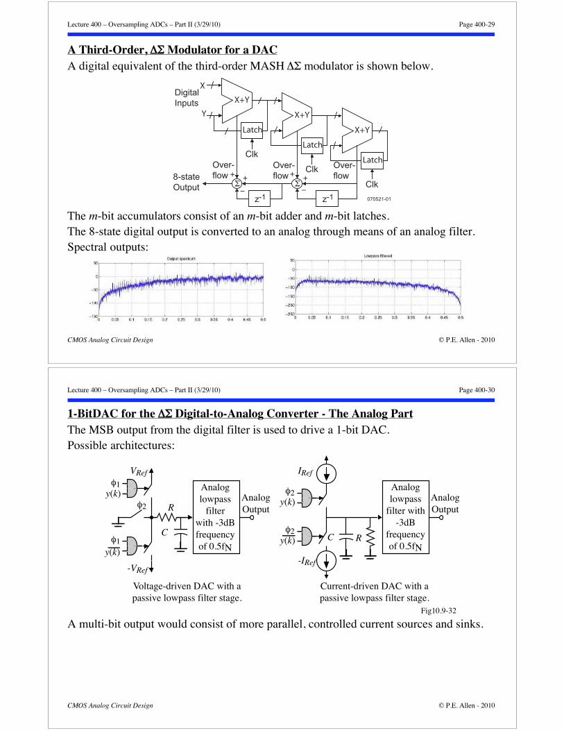
A Third-Order, Modulator for a DACA digital equivalent of the third-order MASH modulator is shown below.
X
Y
X+Y
Latch
Σ
Over-flow
X+Y
Latch
Σ
Over-flow
X+Y
LatchOver-flow
z-1z-1
+ + ++
− −
Clk
Clk
Clk8-stateOutput
DigitalInputs
070521-01
The m-bit accumulators consist of an m-bit adder and m-bit latches.The 8-state digital output is converted to an analog through means of an analog filter.Spectral outputs:
Lecture 400 – Oversampling ADCs – Part II (3/29/10) Page 400-30
CMOS Analog Circuit Design © P.E. Allen - 2010
1-BitDAC for the Digital-to-Analog Converter - The Analog PartThe MSB output from the digital filter is used to drive a 1-bit DAC.Possible architectures:
-VRef
φ1y(k) φ2
y(k)
VRef
φ1y(k)
C R
Analog lowpass
filter with -3dB frequency of 0.5fN
AnalogOutputR
C
φ2
φ2y(k)
Analog lowpass
filter with -3dB
frequency of 0.5fN
AnalogOutput
IRef
-IRef
Voltage-driven DAC with apassive lowpass filter stage.
Current-driven DAC with apassive lowpass filter stage.
Fig10.9-32
A multi-bit output would consist of more parallel, controlled current sources and sinks.

Lecture 400 – Oversampling ADCs – Part II (3/29/10) Page 400-31
CMOS Analog Circuit Design © P.E. Allen - 2010
Switched-Capacitor DAC and FilterTypically, the DAC and the first stage of the lowpass filter are implemented usingswitched-capacitor techniques.
-VRef
φ1y(k)
VRef
φ1y(k)
φ2+-
φ2
φ1
C1
C2
R
To analoglowpass
filter
Fig10.9-34
It is necessary to follow the switched-capacitor filter by a continuous time lowpass filterto provide the necessary attenuation of the quantization noise.
Lecture 400 – Oversampling ADCs – Part II (3/29/10) Page 400-32
CMOS Analog Circuit Design © P.E. Allen - 2010
SUMMARYComparison of the Various Types of ADCs
A/D Converter Type MaximumPractical Number
of Bits (±1)
Speed(Expressed in termsof T a clock period)
Area Dependenceon the number ofbits, N, or otherADC parameters
Dual Slope 12-14 bits 2(2NT) IndependentSuccessive Approximationwith self-correction
12-15 bits NT N
1-Bit Pipeline 10 bits T (After NT delay ) NAlgorithmic 12 bits NT IndependentFlash 6 bits T 2NTwo-step, flash 10-12 bits 2T 2N/2Mulitple-bit, M-pipe 12-14 bits MT 2N/M
- Oversampled (1-bit, Lloops and M= oversamplingratio = f clock/2fb) 15-17 bits MT L

Lecture 400 – Oversampling ADCs – Part II (3/29/10) Page 400-33
CMOS Analog Circuit Design © P.E. Allen - 2010
Comparison of Recent ADCsResolution versus conversion rate:
5
10
15
20
25
Out
put w
ord
leng
th
Conversion rate, (samples/sec.)1 102 104 106 108 1010
Figure 10.10-1
FlashPipelinedAlgorithmic
Dual-slopeDelta-sigma
Successive approximation
Folding/InterpolatingBandpass delta-sigma
Lecture 400 – Oversampling ADCs – Part II (3/29/10) Page 400-34
CMOS Analog Circuit Design © P.E. Allen - 2010
Comparison of Recent ADCs - ContinuedPower dissipation versus conversion rate:
Figure 10.10-2
0.01
0.1
1
10
100
1000
1 100 10 4 10 6 10 8 10 10
Pow
er D
issi
patio
n (m
W)
Conversion Rate (Samples/second)
FlashPipelined
Delta-sigmaSuccessive approximation
Folding/InterpolatingBandpass delta-sigma

Lecture 400 – Oversampling ADCs – Part II (3/29/10) Page 400-35
CMOS Analog Circuit Design © P.E. Allen - 2010
References for Previous Figures [1] A 12-b, 60-MSample/s Cascaded Folding and Interpolating ADC. Vorenkamp, P., IEEE J-SC, vol. 32, no. 12, Dec 97 1876
1886 [2] A 15-b, 5-Msample/s Low-Spurious CMOS ADC. Kwak, S. -U., IEEE J-SC, vol. 32, no. 12, Dec 97 1866-1875 [3] Error Suppressing Encode Logic of FCDL in a 6-b Flash A/D Converter. Ono, K., IEEE J-SC, vol. 32, no.9, Sep 97 1460-
1464 [4] A Cascaded Sigma-Delta Pipeline A/D Converter with 1.25 MHz Signal Bandwidth and 89 dB SNR. Brooks, T. L., IEEE
J-SC, vol.32, no.12, Dec 97 1896-1906 [5] A 10-b, 100 MS/s CMOS A/D Converter. Kwang Young Kim, IEEE J-SC, vol. 32, no. 3, Mar 97 302-311 [6] A 1.95-V, 0.34-mW, 12-b Sigma-Delta Modulator Stabilized by Local Feedback Loops. Au, S., IEEE J-SC, vol. 32, no. 3,
Mar 97 321-328 [7] A 250-mW, 8-b, 52Msamples/s Parallel-Pipelined A/D Converter with Reduced Number of Amplifiers. Nagaraj, K., IEEE J
SC, vol. 32, no. 3, Mar 97 312-320 [8] A DSP-Based Hearing Instrument IC. Neuteboom, H., IEEE J-SC, vol. 32, no. 11, Nov 97 1790-1806 [9] An Embedded 240-mW 10-b 50MS/s CMOS ADC in 1-mm2. Bult, K., IEEE J-SC, vol. 32, no. 12, Dec 97 1887-1895[10] Low-Voltage Double-Sampled Converters. Senderowicz, D., IEEE J-SC, vol. 32, no.12, Dec 97 1907-1919[11] Quadrature Bandpass Modulation for Digital Radio. Jantzi, S. A., IEEE J-SC, vol. 32, no. 12, Dec 97 1935-1950[12] A Two-Path Bandpass Modulator for Digital IF Extraction at 20 MHz. Ong, A. K., IEEE J-SC, vol. 32, no. 12, Dec 97
1920-1934[13] A 240-Mbps, 1-W CMOS EPRML Read-Channel LSI Chip Using an Interleaved Subranging Pipeline A/D Converter.
Matsuura, T., IEEE J-SC, vol. 33, no. 11, Nov 98 1840-1850[14] A 13-Bit, 1.4 MS/s Sigma-Delta Modulator for RF Baseband Channel Applications. Feldman, A. R., IEEE J-SC, vol. 33,
no. 10, Oct 98 1462-1469[15] Design and Implementation of an Untrimmed MOSFET-Only 10-Bit A/D Converter with –79-dB THD. Hammerschmied,
C. M., IEEE J-SC, vol. 33, no. 8, Aug 98 1148-1157[16] A 15-b Resolution 2-MHz Nyquist Rate ADC in a 1-μm CMOS Technology. Marques, A. M., IEEE J-SC, vol. 33, no.
7, Jul 98 1065-1075[17] A 950-MHz IF Second-Order Integrated LC Bandpass Delta-Sigma Modulator. Gao, W., IEEE J-SC, vol. 33, no. 5, May
98 723-732[18] A 200-MSPS 6-Bit Flash ADC in 0.6μm CMOS. Dalton, D., IEEE Transactions on Circuits and Systems II: Analog and
Digital Signal Processing, vol. 45, no. 11, Nov 98 1433-1444
Lecture 400 – Oversampling ADCs – Part II (3/29/10) Page 400-36
CMOS Analog Circuit Design © P.E. Allen - 2010
References - Continued[19] A 5-V Single-Chip Delta-Sigma Audio A/D Converter with 111 dB Dynamic Range. Fujimori, I., IEEE J-SC, vol. 32, no.
3, Mar 97 329-336[20] A 256 x 256 CMOS Imaging Array with Wide Dynamic Range Pixels and Column-Parallel Digital Output. Decker, S.,
IEEE J-SC, vol. 33, no.12, Dec 98 2081-2091[21] A 400 Msample/s, 6-b CMOS Folding and Interpolating ADC. Flynn, M., IEEE J-SC, vol. 33, no.12, Dec 98 1932-1938[22] An Analog Background Calibration Technique for Time-Interleaved Analog-to-Digital Converters. Dyer, K. C., IEEE J-SC,
vol. 33, no.12, Dec 98 1912-1919[23] A CMOS 6-b, 400-Msample/s ADC with Error Correction. Tsukamoto, S., IEEE J-SC, vol. 33, no.12, Dec 98 1939-1947[24] A Continuously Calibrated 12-b, 10-MS/s, 3.3-V ADC. Ingino, J. M., IEEE J-SC, vol. 33, no.12, Dec 98 1920-1931[25] A Delta-Sigma PLL for 14b, 50 ksamples/s Frequency-to-Digital Conversion of a 10 MHz FM Signal. Galton, I., IEEE J-
SC, vol. 33, no.12, Dec 98 2042-2053[26] A Digital Background Calibration Technique for Time-Interleaved Analog-to-Digital Converters. Fu, D., IEEE J-SC, vol. 33
no.12, Dec 98 1904-1911[27] An IEEE 1451 Standard Transducer Interface Chip with 12-b ADC, Two 12-b DAC’s, 10-kB Flash EEPROM, and 8-b
Microcontroller. Cummins, T., IEEE J-SC, vol. 33, no.12, Dec 98 2112-2120[28] A Single-Ended 12-bit 20 Msample/s Self-Calibrating Pipeline A/D Converter. Opris, I. E., IEEE J-SC, vol. 33, no.12, Dec
98 1898-1903[29] A 900-mV Low-Power A/D Converter with 77-dB Dynamic Range. Peluso, V., IEEE J-SC, vol. 33, no.12, Dec 98
1887-1897[30] Third-Order Modulator Using Second-Order Noise-Shaping Dynamic Element Matching. Yasuda, A., IEEE J-SC, vol.
33, no.12, Dec 98 1879-1886[31] R, G, B Acquisition Interface with Line-Locked Clock Generator for Flat Panel Display. Marie, H., IEEE J-SC, vol. 33,
no.7, Jul 98 1009-1013[32] A 25 MS/s 8-b - 10 MS/s 10-b CMOS Data Acquisition IC for Digital Storage Oscilloscopes. Kusayanagi, N., IEEE J-SC,
vol. 33, no.3, Mar 98 492-496[33] A Multimode Digital Detector Readout for Solid-State Medical Imaging Detectors. Boles, C. D., IEEE J-SC, vol. 33, no.5,
May 98 733-742[34] CMOS Charge-Transfer Preamplifier for Offset-Fluctuation Cancellation in Low Power A/D Converters. Kotani, K., IEEE J-
SC, vol. 33, no.5, May 98 762-769[35] Design Techniques for a Low-Power Low-Cost CMOS A/D Converter. Chang, Dong-Young, IEEE J-SC, vol. 33, no.8,
Aug 98 1244-1248

Lecture 400 – Oversampling ADCs – Part II (3/29/10) Page 400-37
CMOS Analog Circuit Design © P.E. Allen - 2010
CONCLUDING THOUGHTS• What is analog circuit design?
The complex process of creating circuit solutions using analog circuit techniques.• What is the analog integrated circuit design process?
The even more complex process of combining analog design with IC technologywhich includes electrical, physical and test design.
• What are the key principles, concepts and techniques for analog IC design?Key principles – Fundamental lawsKey concepts – Important relationships andideas
• How can the analog IC designer enhancecreativity and solve new problems in today’sindustrial environment?
Learn the key principles, concepts and techniques ofanalog circuit designLearn from mistakesLearn the technologyAlways try to understand the concept and operationof the circuit, never rely on a computer or someone else for this understanding
Technology changes but principles, concepts andtechniques remain the same.
Key techniques – Tools that allowsimplification or insight