Embed Size (px)
Citation preview
1SLVA863–December 2016Submit Documentation Feedback
Copyright © 2016, Texas Instruments Incorporated
DiSEqC™ Protocol and Low-Noise Block Voltage Regulator TPS65235 forSatellite – STB/TV
Application ReportSLVA863–December 2016
DiSEqC™ Protocol and Low-Noise Block VoltageRegulator TPS65235 for Satellite – STB/TV
Na Xu
ABSTRACTSatellite STB/TV technology allows consumers to receive TV programming through a personal dishinstalled at their homes or permitted buildings. As the terminal in the signal-channel, the satellite STB/TVreceiver consists of a dish antenna, low-noise block downconverters (LNBs) or external switches, and asatellite-TV decoder. A communication protocol the called Digital Satellite Equipment Control (DiSEqC™)controls the LNBs or external switches.
This application note focuses on how the DiSEqC protocol and LNB function. In addition, two DiSEqCreference designs, based on the LNB voltage regulator TPS65235 from TI, are also discussed.
Contents1 DiSEqC™ System ........................................................................................................... 22 Low-Noise Block Downconverter (LNB) .................................................................................. 43 LNB Voltage Regulator TPS65235 Implementation..................................................................... 54 Summary...................................................................................................................... 95 References .................................................................................................................. 10
List of Figures
1 DiSEqC™ Modulation Scheme ............................................................................................ 22 Timing Diagram for Tone Burst Control Signal .......................................................................... 33 Timing Diagram for DiSEqC™ Level 1.0 ................................................................................. 34 DiSEqC™ Master Command Structure ................................................................................... 45 DiSEqC™ Slave Structure.................................................................................................. 46 LNB Block Diagram.......................................................................................................... 47 TPS65235 DiSEqC™ 1.x Schematic...................................................................................... 58 TPS65235 Output VLNB.................................................................................................... 69 TPS65235 DiSEqC™ 2.x Schematic...................................................................................... 610 TPS65235 Under Accessories Mode ..................................................................................... 711 TPS65235 PC-I2C Software Home Page ................................................................................ 712 TPS65235 PC-I2C Software Register Map Page ....................................................................... 813 TPS65235 PC-I2C Software Basic Settings Page ...................................................................... 9
List of Tables
1 Definition of the DiSEqC™ Levels......................................................................................... 22 Proposed Levels of Implementation for Receivers ...................................................................... 33 Universal LNB Control Manner............................................................................................. 5

DiSEqC™ System www.ti.com
2 SLVA863–December 2016Submit Documentation Feedback
Copyright © 2016, Texas Instruments Incorporated
DiSEqC™ Protocol and Low-Noise Block Voltage Regulator TPS65235 forSatellite – STB/TV
DiSEqC is a trademark of Eutelsat.
1 DiSEqC™ SystemDiSEqC is a communication bus between satellite receivers and peripheral equipment using only theexisting coaxial cable. This protocol is an open standard with additions controlled by an industryagreement developed by the European Telecommunications Satellite Organization (EUTELSAT). DiSEqCcan be integrated into consumer satellite installations to replace conventional analog switching, andminimize the changes required in the tuner-receiver or integrated receiver decoder (IRD).
A prime function of the DiSEqC system is to remotely select between two or more switchable alternatives,like the polarization of received signals. The purpose of the DiSEqC concept is to fix the pin functions (forexample, polarization axis), and also their sense (for example, disabled = vertical polarization).
The DiSEqC system is based on presenting (or not presenting) the 22 kHz tone-signaling method. Theamplitude of this 22-kHz tone signal is 650 mV peak-to-peak with ±250 mV tolerance. To compensate forthe voltage drop on the cable and trace, the detector must be able to respond to the amplitude down, toapproximately 300 mV with ±100 mV tolerance. TI recommends that the maximum amplitude applied inthe bus is 1 V peak-to-peak.
Figure 1. DiSEqC™ Modulation Scheme
With the 22-kHz carrier, the DiSEqC takes a baseband timing of 500 µs with ±100 μs tolerance to transfera 1/3-bit pulse-width-keying (PWK) coded signal period. In the 22-kHz time envelope, there are nominally22 cycles for bit 0, and 11 cycles for bit 1 in each transmitted bit.
The full DiSEqC specification allows multiple different levels of application. The implementation level of theDiSEqC is indicated for clear classification between these levels. Table 1 lists the broad levels.
Table 1. Definition of the DiSEqC™ Levels
Level Control Product TypeDiSEqC compatible Tone Burst command Simple 2-state switches onlyDiSEqC 1.0 One-way DiSEqC commands Receivers onlyDiSEqC 2.0 Two-way DiSEqC commands Receivers and accessories
www.ti.com DiSEqC™ System
3SLVA863–December 2016Submit Documentation Feedback
Copyright © 2016, Texas Instruments Incorporated
DiSEqC™ Protocol and Low-Noise Block Voltage Regulator TPS65235 forSatellite – STB/TV
The DiSEqC can support both the receiver implementation and accessories implementation. Table 2 liststhe definitions of the different DiSEqC levels employed and proposed for receivers.
Table 2. Proposed Levels of Implementation for Receivers
Level Directionality Commands
DiSEqC 1.0 One-way signals Control of at least four committed switches, capability of one repeat, and ToneBurst command
DiSEqC 1.1 One-way signals Same commands as level 1.0, capability of the four uncommitted switches,transmission of up to two repeaters, and remote (head-end) tuning mode
DiSEqC 1.2 One-way signals Same commands as level 1.1, capability of 1-way positioner commands
DiSEqC 2.0 Two-way signals Control of at least four committed switches, capability of one repeat, Tone Burstcommand, LNB L.O frequency reading
DiSEqC 2.1 Two-way signals Same commands as level 2.0, control of the four uncommitted switches, secondrepeat, and remote tuning mode
DiSEqC 2.2 Two-way signals Same commands as level 2.1, positioner commands
The DiSEqC specification was added into the Tone Burst command, which can be detected by simpleanalog hardware. Two types of Tone Burst commands are adopted: the unmodulated to select Satellite A(SA) and the modulated for to select Satellite B (SB). The nominal burst period is 12.5 ms (see Figure 2).For the modulated type, this duration is built up by nine 0.5-ms pulses, and eight 1-ms gaps for bit 1. Themodulation tolerances are ±20%.
Figure 2. Timing Diagram for Tone Burst Control Signal
The timing request of the DiSEqC 1.x (including DiSEqC 1.0, 1.1, and 1.2) is more complex then the ToneBurst command. For DiSEqC 1.0, after the signal DC-voltage change, a gap of more than 15 ms must beobserved to avoid the risk of malfunctions. Another minimum time gap of 15 ms follows the typical fullDiSEqC 1.0 message of 54 ms. The SA/SB Tone Burst arrives before another time gap, which is also of aminimum time gap of 15 ms. A complete DiSEqC tone is built up by the full DiSEqC message, SA/SBTone-Burst, and three time gaps (see Figure 3).
To avoid disturbing the simple analog hardware of the Tone Burst detector, ensure that the DC voltage-signaling step arrives long before the Tone Burst.
Figure 3. Timing Diagram for DiSEqC™ Level 1.0
Framing P Data P Data P
Framing P Address P Command P Data P
Low-Noise Block Downconverter (LNB) www.ti.com
4 SLVA863–December 2016Submit Documentation Feedback
Copyright © 2016, Texas Instruments Incorporated
DiSEqC™ Protocol and Low-Noise Block Voltage Regulator TPS65235 forSatellite – STB/TV
The recommended DiSEqC 2.x (including DiSEqC 2.0, 2.1, and 2.2) tone timing is similar to DiSEqC 1.x.The difference is that between the message and the next tone, the master must leave a time gap of atleast 150 ms. The DiSEqC command is built up by the master command and the slave reply. The mastercommand is for both the DiSEqC 1.x and the DiSEqC 2.x; the slave relay is for DiSEqC 2.x, or above forthe backward signal. The master command consists of the framing byte, address byte, and commandbyte. Sometimes an additional data byte is also carried in the command. The framing byte includes somehigh-level control and the slave address is marked in the address byte (see Figure 4).
Figure 4. DiSEqC™ Master Command Structure
The slave reply starts with the framing byte and the framing byte is followed by 1 or more data bytes (seeFigure 5). The slave reply should take no more than 150 ms from the end of the command message.
Figure 5. DiSEqC™ Slave Structure
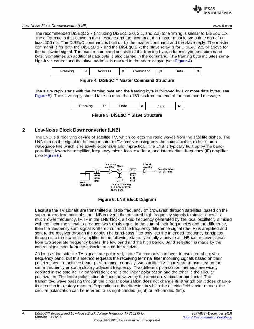
2 Low-Noise Block Downconverter (LNB)The LNB is a receiving device of satellite TV, which collects the radio waves from the satellite dishes. TheLNB carries the signal to the indoor satellite TV receiver using only the coaxial cable, rather than awaveguide line which is relatively expensive and impractical. The LNB is typically built up by the band-pass filter, low-noise amplifier, frequency mixer, local oscillator, and intermediate frequency (IF) amplifier(see Figure 6).
Figure 6. LNB Block Diagram
Because the TV signals are transmitted at radio frequency (microwaves) through satellites, based on thesuper-heterodyne principle, the LNB converts the captured high-frequency signals to similar ones at amuch lower frequency, IF. IF in the LNB block, a fixed frequency generated by the local oscillator, is mixedwith the incoming signal to produce two signals equal to the sum of their frequencies and the difference,then the frequency sum signal is filtered out and the frequency difference signal (the IF) is amplified andsent to the receiver through the cable. The band-pass filter only lets the intended frequency bandpassthrough it to the low-noise amplifier in the following stage. Normally a universal LNB can receive signalsfrom two separate frequency bands (the low band and the high band). Band selection is made by thecontrol signal sent from the associated satellite receiver.
As long as the satellite TV signals are polarized, more TV channels can been transmitted at a givenfrequency band, but this method requests the receiving terminal filter incoming signals based on theirpolarizations. To achieve better performance, normally two satellite TV signals are transmitted on thesame frequency or some closely adjacent frequency. Two different polarization methods are widelyadopted in the satellite TV transmission; one is the linear polarization and the other is the circularpolarization. The linear polarization defines the wave by the direction, vertical or horizontal. Thetransmitted wave passing through the circular polarization does not change its strength but it does changeits direction in a rotary manner. Depending on the direction in which the electric field vector rotates, thecircular polarization can be referred to as right-handed (right) or left-handed (left).
www.ti.com LNB Voltage Regulator TPS65235 Implementation
5SLVA863–December 2016Submit Documentation Feedback
Copyright © 2016, Texas Instruments Incorporated
DiSEqC™ Protocol and Low-Noise Block Voltage Regulator TPS65235 forSatellite – STB/TV
In universal LNB, the band selection (high and low band) is controlled by presenting the 22-kHz tone withspecific definition of the DiSEqC protocol. The polarization is decided by the receiver through two differentDC signal levels, normally a 13-V signal and a 18-V signal (Table 3).
Table 3. Universal LNB Control Manner
Power Band Polarization13 V Low Vertical, right18 V Low Horizontal, left13 V + 22 kHz High Vertical, right18 V + 22 kHz High Horizontal, left
3 LNB Voltage Regulator TPS65235 Implementation
3.1 Brief IntroductionBecause the universal LNB is controlled by DC signal levels and 22-kHz tone presentation, a monolithicsemiconductor IC, which can provide both 13-V and 18-V DC signal and the 22-kHz tone, is ideal for thedesign of the LNB and minimizes the total BOM size. The TPS65235 device from TI is the voltageregulator supporting both DiSEqC 1.x and DiSEqC 2.x, and offers a complete solution for the LNB withsimple design and I2C standard interface. For more details, see the TPS65235 data sheet.
3.2 Component Selection Guidelines
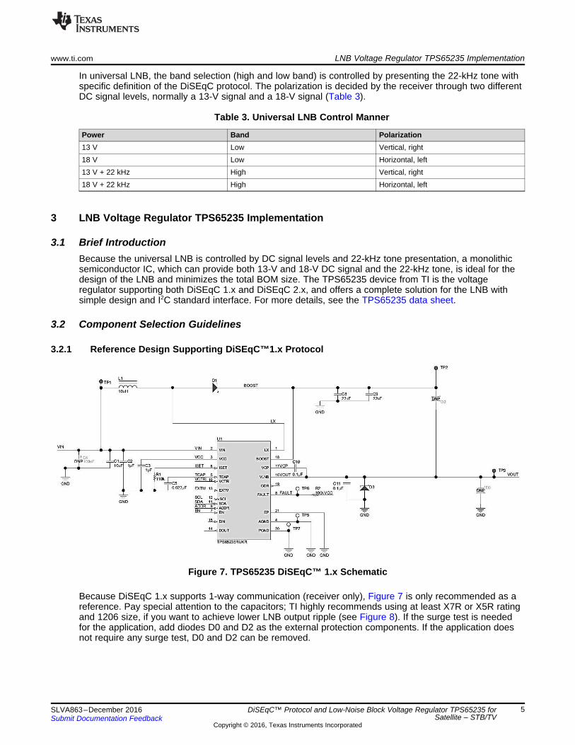
3.2.1 Reference Design Supporting DiSEqC™1.x Protocol
Figure 7. TPS65235 DiSEqC™ 1.x Schematic
Because DiSEqC 1.x supports 1-way communication (receiver only), Figure 7 is only recommended as areference. Pay special attention to the capacitors; TI highly recommends using at least X7R or X5R ratingand 1206 size, if you want to achieve lower LNB output ripple (see Figure 8). If the surge test is neededfor the application, add diodes D0 and D2 as the external protection components. If the application doesnot require any surge test, D0 and D2 can be removed.
LNB Voltage Regulator TPS65235 Implementation www.ti.com
6 SLVA863–December 2016Submit Documentation Feedback
Copyright © 2016, Texas Instruments Incorporated
DiSEqC™ Protocol and Low-Noise Block Voltage Regulator TPS65235 forSatellite – STB/TV
Figure 8. TPS65235 Output VLNB
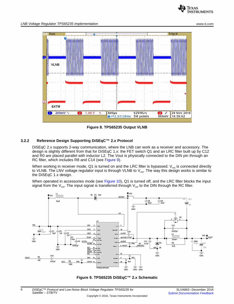
3.2.2 Reference Design Supporting DiSEqC™ 2.x ProtocolDiSEqC 2.x supports 2-way communication, where the LNB can work as a receiver and accessory. Thedesign is slightly different from that for DiSEqC 1.x: the FET switch Q1 and an LRC filter built up by C12and R0 are placed parallel with inductor L2. The Vout is physically connected to the DIN pin through anRC filter, which includes R8 and C14 (see Figure 9).
When working in receiver mode, Q1 is turned on and the LRC filter is bypassed. Vout is connected directlyto VLNB. The LNV voltage regulator input is through VLNB to Vout. The way this design works is similar tothe DiSEqC 1.x design.
When operated in accessories mode (see Figure 10), Q1 is turned off, and the LRC filter blocks the inputsignal from the Vout. The input signal is transferred through Vout to the DIN through the RC filter.
Figure 9. TPS65235 DiSEqC™ 2.x Schematic
www.ti.com LNB Voltage Regulator TPS65235 Implementation
7SLVA863–December 2016Submit Documentation Feedback
Copyright © 2016, Texas Instruments Incorporated
DiSEqC™ Protocol and Low-Noise Block Voltage Regulator TPS65235 forSatellite – STB/TV
As recommended in the design for DiSEqC 1.x, diodes D0 and D2 are optional. If the application does notrequire any surge test, these two diodes are removable. The 0.1-µF output capacitor marked DNP in theschematic is the filter capacitor; it can be removed if the system performance is sufficient.
Figure 10. TPS65235 Under Accessories Mode
To achieve lower LNB output ripple, TI highly recommends using capacitors at least X7R or X5R ratingand 1206 size.
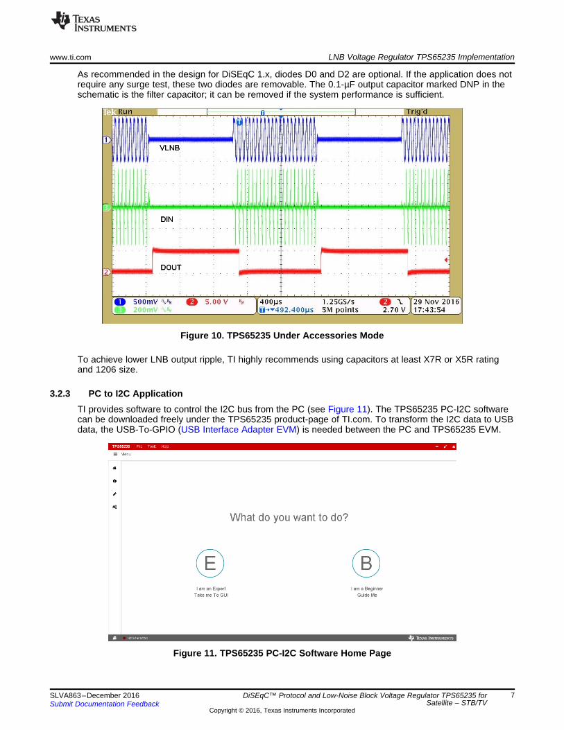
3.2.3 PC to I2C ApplicationTI provides software to control the I2C bus from the PC (see Figure 11). The TPS65235 PC-I2C softwarecan be downloaded freely under the TPS65235 product-page of TI.com. To transform the I2C data to USBdata, the USB-To-GPIO (USB Interface Adapter EVM) is needed between the PC and TPS65235 EVM.
Figure 11. TPS65235 PC-I2C Software Home Page

LNB Voltage Regulator TPS65235 Implementation www.ti.com
8 SLVA863–December 2016Submit Documentation Feedback
Copyright © 2016, Texas Instruments Incorporated
DiSEqC™ Protocol and Low-Noise Block Voltage Regulator TPS65235 forSatellite – STB/TV
After opening the TPS65235 PC-I2C software window, the program detects the USB-To-GPIO box first,and initializes the I2C system registers of the TPS65235. The status of the connection is shown by theindicator on the lower right side. If this is the first time you have opened this software, you may need tofirst select the proper device I2C address based on your design. You can make your I2C addressselection in two places (see Figure 12).
Figure 12. TPS65235 PC-I2C Software Register Map Page
To evaluate the TPS65235 functionality by toggling the system register bits, do the following:1. Click the Register Map button on the left side of the screen.2. On the Register Map page, select the I2C address of the design on the top-center of the window.3. When the software has detected the TPS65235, and indicated the PC is connected to the TPS65235,
you can make the register read or write action directly on the software by clicking on the target registerbit and read/write register bottom.
www.ti.com Summary
9SLVA863–December 2016Submit Documentation Feedback
Copyright © 2016, Texas Instruments Incorporated
DiSEqC™ Protocol and Low-Noise Block Voltage Regulator TPS65235 forSatellite – STB/TV
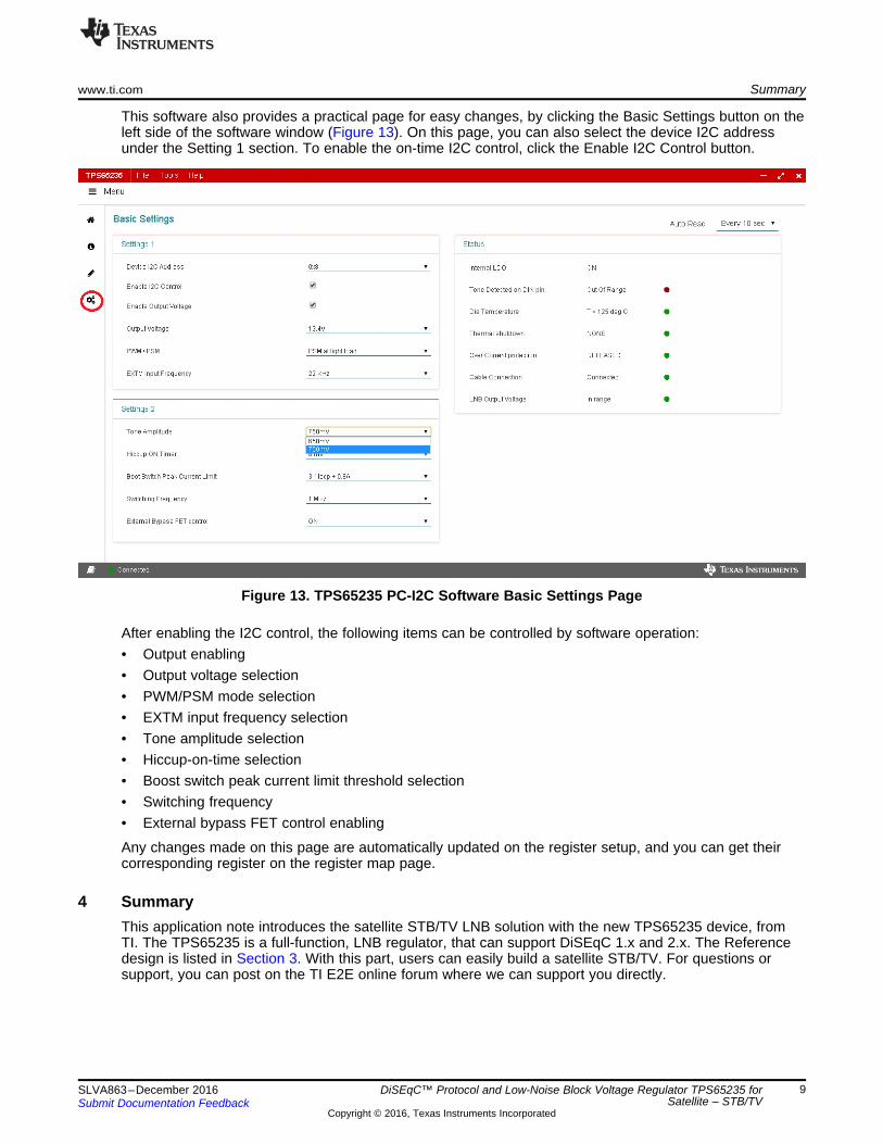
This software also provides a practical page for easy changes, by clicking the Basic Settings button on theleft side of the software window (Figure 13). On this page, you can also select the device I2C addressunder the Setting 1 section. To enable the on-time I2C control, click the Enable I2C Control button.
Figure 13. TPS65235 PC-I2C Software Basic Settings Page
After enabling the I2C control, the following items can be controlled by software operation:• Output enabling• Output voltage selection• PWM/PSM mode selection• EXTM input frequency selection• Tone amplitude selection• Hiccup-on-time selection• Boost switch peak current limit threshold selection• Switching frequency• External bypass FET control enabling
Any changes made on this page are automatically updated on the register setup, and you can get theircorresponding register on the register map page.
4 SummaryThis application note introduces the satellite STB/TV LNB solution with the new TPS65235 device, fromTI. The TPS65235 is a full-function, LNB regulator, that can support DiSEqC 1.x and 2.x. The Referencedesign is listed in Section 3. With this part, users can easily build a satellite STB/TV. For questions orsupport, you can post on the TI E2E online forum where we can support you directly.
References www.ti.com
10 SLVA863–December 2016Submit Documentation Feedback
Copyright © 2016, Texas Instruments Incorporated
DiSEqC™ Protocol and Low-Noise Block Voltage Regulator TPS65235 forSatellite – STB/TV
5 References1. Digital Satellite Equipment Control Bus Functional Specification Version 4.2, European
Telecommunications Satellite Organization, Feb. 25, 19982. Digital Satellite Equipment Control (DiSEqC™ ) Update and Recommendations for Implementation
Version 2.1, European Telecommunications Satellite Organization, Feb. 25, 19983. DiSEqC™ 2.0 for Technicians, Klaus Muller, SPAUN Electronic4. TV Explorer and DiSEqC™, Promax ELECTRONICA, S.A.5. Evaluation Module for the TPS65235 LNB Voltage Regulator With I²C Interface, User's Guide6. TPS65235 EVM User Guide for DisEqC 2.x Application, User's Guide
IMPORTANT NOTICE
Texas Instruments Incorporated and its subsidiaries (TI) reserve the right to make corrections, enhancements, improvements and otherchanges to its semiconductor products and services per JESD46, latest issue, and to discontinue any product or service per JESD48, latestissue. Buyers should obtain the latest relevant information before placing orders and should verify that such information is current andcomplete. All semiconductor products (also referred to herein as “components”) are sold subject to TI’s terms and conditions of salesupplied at the time of order acknowledgment.TI warrants performance of its components to the specifications applicable at the time of sale, in accordance with the warranty in TI’s termsand conditions of sale of semiconductor products. Testing and other quality control techniques are used to the extent TI deems necessaryto support this warranty. Except where mandated by applicable law, testing of all parameters of each component is not necessarilyperformed.TI assumes no liability for applications assistance or the design of Buyers’ products. Buyers are responsible for their products andapplications using TI components. To minimize the risks associated with Buyers’ products and applications, Buyers should provideadequate design and operating safeguards.TI does not warrant or represent that any license, either express or implied, is granted under any patent right, copyright, mask work right, orother intellectual property right relating to any combination, machine, or process in which TI components or services are used. Informationpublished by TI regarding third-party products or services does not constitute a license to use such products or services or a warranty orendorsement thereof. Use of such information may require a license from a third party under the patents or other intellectual property of thethird party, or a license from TI under the patents or other intellectual property of TI.Reproduction of significant portions of TI information in TI data books or data sheets is permissible only if reproduction is without alterationand is accompanied by all associated warranties, conditions, limitations, and notices. TI is not responsible or liable for such altereddocumentation. Information of third parties may be subject to additional restrictions.Resale of TI components or services with statements different from or beyond the parameters stated by TI for that component or servicevoids all express and any implied warranties for the associated TI component or service and is an unfair and deceptive business practice.TI is not responsible or liable for any such statements.Buyer acknowledges and agrees that it is solely responsible for compliance with all legal, regulatory and safety-related requirementsconcerning its products, and any use of TI components in its applications, notwithstanding any applications-related information or supportthat may be provided by TI. Buyer represents and agrees that it has all the necessary expertise to create and implement safeguards whichanticipate dangerous consequences of failures, monitor failures and their consequences, lessen the likelihood of failures that might causeharm and take appropriate remedial actions. Buyer will fully indemnify TI and its representatives against any damages arising out of the useof any TI components in safety-critical applications.In some cases, TI components may be promoted specifically to facilitate safety-related applications. With such components, TI’s goal is tohelp enable customers to design and create their own end-product solutions that meet applicable functional safety standards andrequirements. Nonetheless, such components are subject to these terms.No TI components are authorized for use in FDA Class III (or similar life-critical medical equipment) unless authorized officers of the partieshave executed a special agreement specifically governing such use.Only those TI components which TI has specifically designated as military grade or “enhanced plastic” are designed and intended for use inmilitary/aerospace applications or environments. Buyer acknowledges and agrees that any military or aerospace use of TI componentswhich have not been so designated is solely at the Buyer's risk, and that Buyer is solely responsible for compliance with all legal andregulatory requirements in connection with such use.TI has specifically designated certain components as meeting ISO/TS16949 requirements, mainly for automotive use. In any case of use ofnon-designated products, TI will not be responsible for any failure to meet ISO/TS16949.
Products ApplicationsAudio www.ti.com/audio Automotive and Transportation www.ti.com/automotiveAmplifiers amplifier.ti.com Communications and Telecom www.ti.com/communicationsData Converters dataconverter.ti.com Computers and Peripherals www.ti.com/computersDLP® Products www.dlp.com Consumer Electronics www.ti.com/consumer-appsDSP dsp.ti.com Energy and Lighting www.ti.com/energyClocks and Timers www.ti.com/clocks Industrial www.ti.com/industrialInterface interface.ti.com Medical www.ti.com/medicalLogic logic.ti.com Security www.ti.com/securityPower Mgmt power.ti.com Space, Avionics and Defense www.ti.com/space-avionics-defenseMicrocontrollers microcontroller.ti.com Video and Imaging www.ti.com/videoRFID www.ti-rfid.comOMAP Applications Processors www.ti.com/omap TI E2E Community e2e.ti.comWireless Connectivity www.ti.com/wirelessconnectivity
Mailing Address: Texas Instruments, Post Office Box 655303, Dallas, Texas 75265Copyright © 2016, Texas Instruments Incorporated